EP3902019A1 - Tandemsolarzelle - Google Patents
Tandemsolarzelle Download PDFInfo
- Publication number
- EP3902019A1 EP3902019A1 EP19900237.9A EP19900237A EP3902019A1 EP 3902019 A1 EP3902019 A1 EP 3902019A1 EP 19900237 A EP19900237 A EP 19900237A EP 3902019 A1 EP3902019 A1 EP 3902019A1
- Authority
- EP
- European Patent Office
- Prior art keywords
- solar cell
- layer
- conductive type
- type semiconductor
- semiconductor layer
- Prior art date
- Legal status (The legal status is an assumption and is not a legal conclusion. Google has not performed a legal analysis and makes no representation as to the accuracy of the status listed.)
- Pending
Links
- XUIMIQQOPSSXEZ-UHFFFAOYSA-N Silicon Chemical compound [Si] XUIMIQQOPSSXEZ-UHFFFAOYSA-N 0.000 claims abstract description 135
- 229910052710 silicon Inorganic materials 0.000 claims abstract description 135
- 239000010703 silicon Substances 0.000 claims abstract description 135
- 238000010521 absorption reaction Methods 0.000 claims abstract description 30
- 239000004065 semiconductor Substances 0.000 claims description 172
- 229910021419 crystalline silicon Inorganic materials 0.000 claims description 74
- 239000000758 substrate Substances 0.000 claims description 67
- 229910052739 hydrogen Inorganic materials 0.000 claims description 54
- 239000001257 hydrogen Substances 0.000 claims description 54
- 239000012535 impurity Substances 0.000 claims description 51
- UFHFLCQGNIYNRP-UHFFFAOYSA-N Hydrogen Chemical compound [H][H] UFHFLCQGNIYNRP-UHFFFAOYSA-N 0.000 claims description 50
- GPRLSGONYQIRFK-UHFFFAOYSA-N hydron Chemical compound [H+] GPRLSGONYQIRFK-UHFFFAOYSA-N 0.000 claims description 39
- 229910021420 polycrystalline silicon Inorganic materials 0.000 claims description 36
- 238000000034 method Methods 0.000 claims description 32
- 238000002161 passivation Methods 0.000 claims description 20
- 230000005525 hole transport Effects 0.000 claims description 14
- 238000004519 manufacturing process Methods 0.000 claims description 14
- 238000000059 patterning Methods 0.000 claims description 13
- 230000007547 defect Effects 0.000 claims description 10
- 238000002513 implantation Methods 0.000 claims description 9
- 239000004020 conductor Substances 0.000 claims description 5
- 238000003486 chemical etching Methods 0.000 claims description 4
- 229920001940 conductive polymer Polymers 0.000 claims description 4
- 150000004820 halides Chemical class 0.000 claims description 3
- 229910001507 metal halide Inorganic materials 0.000 claims description 3
- 150000005309 metal halides Chemical class 0.000 claims description 3
- 239000007769 metal material Substances 0.000 claims description 3
- 125000004435 hydrogen atom Chemical group [H]* 0.000 claims description 2
- 229910021423 nanocrystalline silicon Inorganic materials 0.000 claims description 2
- 239000002861 polymer material Substances 0.000 claims description 2
- 230000003471 anti-radiation Effects 0.000 claims 2
- 239000010410 layer Substances 0.000 description 298
- 239000000969 carrier Substances 0.000 description 26
- 230000006798 recombination Effects 0.000 description 13
- 238000005215 recombination Methods 0.000 description 13
- 238000006243 chemical reaction Methods 0.000 description 12
- VYPSYNLAJGMNEJ-UHFFFAOYSA-N Silicium dioxide Chemical compound O=[Si]=O VYPSYNLAJGMNEJ-UHFFFAOYSA-N 0.000 description 6
- 229910052814 silicon oxide Inorganic materials 0.000 description 6
- 238000004518 low pressure chemical vapour deposition Methods 0.000 description 5
- 239000000463 material Substances 0.000 description 5
- 230000000694 effects Effects 0.000 description 4
- TWNQGVIAIRXVLR-UHFFFAOYSA-N oxo(oxoalumanyloxy)alumane Chemical compound O=[Al]O[Al]=O TWNQGVIAIRXVLR-UHFFFAOYSA-N 0.000 description 4
- HQVNEWCFYHHQES-UHFFFAOYSA-N silicon nitride Chemical compound N12[Si]34N5[Si]62N3[Si]51N64 HQVNEWCFYHHQES-UHFFFAOYSA-N 0.000 description 4
- 230000005641 tunneling Effects 0.000 description 4
- PXHVJJICTQNCMI-UHFFFAOYSA-N Nickel Chemical compound [Ni] PXHVJJICTQNCMI-UHFFFAOYSA-N 0.000 description 3
- -1 halogen anion Chemical group 0.000 description 3
- 229910052751 metal Inorganic materials 0.000 description 3
- 239000002184 metal Substances 0.000 description 3
- 239000010936 titanium Substances 0.000 description 3
- OKTJSMMVPCPJKN-UHFFFAOYSA-N Carbon Chemical compound [C] OKTJSMMVPCPJKN-UHFFFAOYSA-N 0.000 description 2
- 229920000144 PEDOT:PSS Polymers 0.000 description 2
- NBIIXXVUZAFLBC-UHFFFAOYSA-N Phosphoric acid Chemical compound OP(O)(O)=O NBIIXXVUZAFLBC-UHFFFAOYSA-N 0.000 description 2
- 229910052581 Si3N4 Inorganic materials 0.000 description 2
- GWEVSGVZZGPLCZ-UHFFFAOYSA-N Titan oxide Chemical compound O=[Ti]=O GWEVSGVZZGPLCZ-UHFFFAOYSA-N 0.000 description 2
- 229910052782 aluminium Inorganic materials 0.000 description 2
- XAGFODPZIPBFFR-UHFFFAOYSA-N aluminium Chemical compound [Al] XAGFODPZIPBFFR-UHFFFAOYSA-N 0.000 description 2
- QHJPGANWSLEMTI-UHFFFAOYSA-N aminomethylideneazanium;iodide Chemical compound I.NC=N QHJPGANWSLEMTI-UHFFFAOYSA-N 0.000 description 2
- 229910021417 amorphous silicon Inorganic materials 0.000 description 2
- ILAHWRKJUDSMFH-UHFFFAOYSA-N boron tribromide Chemical compound BrB(Br)Br ILAHWRKJUDSMFH-UHFFFAOYSA-N 0.000 description 2
- 150000001768 cations Chemical class 0.000 description 2
- 238000005229 chemical vapour deposition Methods 0.000 description 2
- 150000001875 compounds Chemical class 0.000 description 2
- 239000010949 copper Substances 0.000 description 2
- 238000009792 diffusion process Methods 0.000 description 2
- 239000010931 gold Substances 0.000 description 2
- 229910052738 indium Inorganic materials 0.000 description 2
- APFVFJFRJDLVQX-UHFFFAOYSA-N indium atom Chemical compound [In] APFVFJFRJDLVQX-UHFFFAOYSA-N 0.000 description 2
- LLWRXQXPJMPHLR-UHFFFAOYSA-N methylazanium;iodide Chemical compound [I-].[NH3+]C LLWRXQXPJMPHLR-UHFFFAOYSA-N 0.000 description 2
- XHXFXVLFKHQFAL-UHFFFAOYSA-N phosphoryl trichloride Chemical compound ClP(Cl)(Cl)=O XHXFXVLFKHQFAL-UHFFFAOYSA-N 0.000 description 2
- 238000007747 plating Methods 0.000 description 2
- 238000007650 screen-printing Methods 0.000 description 2
- 239000002356 single layer Substances 0.000 description 2
- 238000001228 spectrum Methods 0.000 description 2
- 238000004528 spin coating Methods 0.000 description 2
- 238000004544 sputter deposition Methods 0.000 description 2
- 238000002207 thermal evaporation Methods 0.000 description 2
- OGIDPMRJRNCKJF-UHFFFAOYSA-N titanium oxide Inorganic materials [Ti]=O OGIDPMRJRNCKJF-UHFFFAOYSA-N 0.000 description 2
- XDXWNHPWWKGTKO-UHFFFAOYSA-N 207739-72-8 Chemical compound C1=CC(OC)=CC=C1N(C=1C=C2C3(C4=CC(=CC=C4C2=CC=1)N(C=1C=CC(OC)=CC=1)C=1C=CC(OC)=CC=1)C1=CC(=CC=C1C1=CC=C(C=C13)N(C=1C=CC(OC)=CC=1)C=1C=CC(OC)=CC=1)N(C=1C=CC(OC)=CC=1)C=1C=CC(OC)=CC=1)C1=CC=C(OC)C=C1 XDXWNHPWWKGTKO-UHFFFAOYSA-N 0.000 description 1
- QGZKDVFQNNGYKY-UHFFFAOYSA-O Ammonium Chemical compound [NH4+] QGZKDVFQNNGYKY-UHFFFAOYSA-O 0.000 description 1
- ZOXJGFHDIHLPTG-UHFFFAOYSA-N Boron Chemical compound [B] ZOXJGFHDIHLPTG-UHFFFAOYSA-N 0.000 description 1
- XMWRBQBLMFGWIX-UHFFFAOYSA-N C60 fullerene Chemical compound C12=C3C(C4=C56)=C7C8=C5C5=C9C%10=C6C6=C4C1=C1C4=C6C6=C%10C%10=C9C9=C%11C5=C8C5=C8C7=C3C3=C7C2=C1C1=C2C4=C6C4=C%10C6=C9C9=C%11C5=C5C8=C3C3=C7C1=C1C2=C4C6=C2C9=C5C3=C12 XMWRBQBLMFGWIX-UHFFFAOYSA-N 0.000 description 1
- RYGMFSIKBFXOCR-UHFFFAOYSA-N Copper Chemical compound [Cu] RYGMFSIKBFXOCR-UHFFFAOYSA-N 0.000 description 1
- GYHNNYVSQQEPJS-UHFFFAOYSA-N Gallium Chemical compound [Ga] GYHNNYVSQQEPJS-UHFFFAOYSA-N 0.000 description 1
- OAICVXFJPJFONN-UHFFFAOYSA-N Phosphorus Chemical compound [P] OAICVXFJPJFONN-UHFFFAOYSA-N 0.000 description 1
- 229910004012 SiCx Inorganic materials 0.000 description 1
- BQCADISMDOOEFD-UHFFFAOYSA-N Silver Chemical compound [Ag] BQCADISMDOOEFD-UHFFFAOYSA-N 0.000 description 1
- 229910006404 SnO 2 Inorganic materials 0.000 description 1
- 229910010413 TiO 2 Inorganic materials 0.000 description 1
- ATJFFYVFTNAWJD-UHFFFAOYSA-N Tin Chemical compound [Sn] ATJFFYVFTNAWJD-UHFFFAOYSA-N 0.000 description 1
- RTAQQCXQSZGOHL-UHFFFAOYSA-N Titanium Chemical compound [Ti] RTAQQCXQSZGOHL-UHFFFAOYSA-N 0.000 description 1
- 239000006096 absorbing agent Substances 0.000 description 1
- 239000002253 acid Substances 0.000 description 1
- 229910000147 aluminium phosphate Inorganic materials 0.000 description 1
- 150000001412 amines Chemical class 0.000 description 1
- 229910052787 antimony Inorganic materials 0.000 description 1
- WATWJIUSRGPENY-UHFFFAOYSA-N antimony atom Chemical compound [Sb] WATWJIUSRGPENY-UHFFFAOYSA-N 0.000 description 1
- 229910052785 arsenic Inorganic materials 0.000 description 1
- RQNWIZPPADIBDY-UHFFFAOYSA-N arsenic atom Chemical compound [As] RQNWIZPPADIBDY-UHFFFAOYSA-N 0.000 description 1
- 230000005540 biological transmission Effects 0.000 description 1
- 229910052797 bismuth Inorganic materials 0.000 description 1
- JCXGWMGPZLAOME-UHFFFAOYSA-N bismuth atom Chemical compound [Bi] JCXGWMGPZLAOME-UHFFFAOYSA-N 0.000 description 1
- 229910052796 boron Inorganic materials 0.000 description 1
- 239000002041 carbon nanotube Substances 0.000 description 1
- 229910021393 carbon nanotube Inorganic materials 0.000 description 1
- 238000010276 construction Methods 0.000 description 1
- 229910052802 copper Inorganic materials 0.000 description 1
- 239000013078 crystal Substances 0.000 description 1
- 238000000151 deposition Methods 0.000 description 1
- 230000008021 deposition Effects 0.000 description 1
- ZOCHARZZJNPSEU-UHFFFAOYSA-N diboron Chemical compound B#B ZOCHARZZJNPSEU-UHFFFAOYSA-N 0.000 description 1
- 239000003989 dielectric material Substances 0.000 description 1
- 238000005516 engineering process Methods 0.000 description 1
- 238000005530 etching Methods 0.000 description 1
- 229910003472 fullerene Inorganic materials 0.000 description 1
- 229910052733 gallium Inorganic materials 0.000 description 1
- 239000011521 glass Substances 0.000 description 1
- PCHJSUWPFVWCPO-UHFFFAOYSA-N gold Chemical compound [Au] PCHJSUWPFVWCPO-UHFFFAOYSA-N 0.000 description 1
- 229910052737 gold Inorganic materials 0.000 description 1
- 229910021389 graphene Inorganic materials 0.000 description 1
- 229910021478 group 5 element Inorganic materials 0.000 description 1
- 229910052736 halogen Inorganic materials 0.000 description 1
- 238000010438 heat treatment Methods 0.000 description 1
- XMBWDFGMSWQBCA-UHFFFAOYSA-N hydrogen iodide Chemical compound I XMBWDFGMSWQBCA-UHFFFAOYSA-N 0.000 description 1
- CBEQRNSPHCCXSH-UHFFFAOYSA-N iodine monobromide Chemical compound IBr CBEQRNSPHCCXSH-UHFFFAOYSA-N 0.000 description 1
- 238000005468 ion implantation Methods 0.000 description 1
- 230000001788 irregular Effects 0.000 description 1
- HWSZZLVAJGOAAY-UHFFFAOYSA-L lead(II) chloride Chemical compound Cl[Pb]Cl HWSZZLVAJGOAAY-UHFFFAOYSA-L 0.000 description 1
- 239000011777 magnesium Substances 0.000 description 1
- ORUIBWPALBXDOA-UHFFFAOYSA-L magnesium fluoride Chemical compound [F-].[F-].[Mg+2] ORUIBWPALBXDOA-UHFFFAOYSA-L 0.000 description 1
- 239000000203 mixture Substances 0.000 description 1
- 238000012986 modification Methods 0.000 description 1
- 230000004048 modification Effects 0.000 description 1
- 229910052759 nickel Inorganic materials 0.000 description 1
- 230000003287 optical effect Effects 0.000 description 1
- 239000005416 organic matter Substances 0.000 description 1
- 230000003647 oxidation Effects 0.000 description 1
- 238000007254 oxidation reaction Methods 0.000 description 1
- 229910052698 phosphorus Inorganic materials 0.000 description 1
- 239000011574 phosphorus Substances 0.000 description 1
- 238000005240 physical vapour deposition Methods 0.000 description 1
- 229920000767 polyaniline Polymers 0.000 description 1
- 229920000128 polypyrrole Polymers 0.000 description 1
- 229920000123 polythiophene Polymers 0.000 description 1
- HBMJWWWQQXIZIP-UHFFFAOYSA-N silicon carbide Chemical compound [Si+]#[C-] HBMJWWWQQXIZIP-UHFFFAOYSA-N 0.000 description 1
- 229910010271 silicon carbide Inorganic materials 0.000 description 1
- 229910052709 silver Inorganic materials 0.000 description 1
- 239000004332 silver Substances 0.000 description 1
- JBQYATWDVHIOAR-UHFFFAOYSA-N tellanylidenegermanium Chemical compound [Te]=[Ge] JBQYATWDVHIOAR-UHFFFAOYSA-N 0.000 description 1
- 229910052719 titanium Inorganic materials 0.000 description 1
- 238000007740 vapor deposition Methods 0.000 description 1
- 239000011701 zinc Substances 0.000 description 1
- XLOMVQKBTHCTTD-UHFFFAOYSA-N zinc oxide Inorganic materials [Zn]=O XLOMVQKBTHCTTD-UHFFFAOYSA-N 0.000 description 1
Images

Classifications
-
- H—ELECTRICITY
- H01—ELECTRIC ELEMENTS
- H01L—SEMICONDUCTOR DEVICES NOT COVERED BY CLASS H10
- H01L31/00—Semiconductor devices sensitive to infrared radiation, light, electromagnetic radiation of shorter wavelength or corpuscular radiation and specially adapted either for the conversion of the energy of such radiation into electrical energy or for the control of electrical energy by such radiation; Processes or apparatus specially adapted for the manufacture or treatment thereof or of parts thereof; Details thereof
- H01L31/04—Semiconductor devices sensitive to infrared radiation, light, electromagnetic radiation of shorter wavelength or corpuscular radiation and specially adapted either for the conversion of the energy of such radiation into electrical energy or for the control of electrical energy by such radiation; Processes or apparatus specially adapted for the manufacture or treatment thereof or of parts thereof; Details thereof adapted as photovoltaic [PV] conversion devices
- H01L31/06—Semiconductor devices sensitive to infrared radiation, light, electromagnetic radiation of shorter wavelength or corpuscular radiation and specially adapted either for the conversion of the energy of such radiation into electrical energy or for the control of electrical energy by such radiation; Processes or apparatus specially adapted for the manufacture or treatment thereof or of parts thereof; Details thereof adapted as photovoltaic [PV] conversion devices characterised by potential barriers
- H01L31/072—Semiconductor devices sensitive to infrared radiation, light, electromagnetic radiation of shorter wavelength or corpuscular radiation and specially adapted either for the conversion of the energy of such radiation into electrical energy or for the control of electrical energy by such radiation; Processes or apparatus specially adapted for the manufacture or treatment thereof or of parts thereof; Details thereof adapted as photovoltaic [PV] conversion devices characterised by potential barriers the potential barriers being only of the PN heterojunction type
- H01L31/0725—Multiple junction or tandem solar cells
-
- H—ELECTRICITY
- H01—ELECTRIC ELEMENTS
- H01L—SEMICONDUCTOR DEVICES NOT COVERED BY CLASS H10
- H01L31/00—Semiconductor devices sensitive to infrared radiation, light, electromagnetic radiation of shorter wavelength or corpuscular radiation and specially adapted either for the conversion of the energy of such radiation into electrical energy or for the control of electrical energy by such radiation; Processes or apparatus specially adapted for the manufacture or treatment thereof or of parts thereof; Details thereof
- H01L31/04—Semiconductor devices sensitive to infrared radiation, light, electromagnetic radiation of shorter wavelength or corpuscular radiation and specially adapted either for the conversion of the energy of such radiation into electrical energy or for the control of electrical energy by such radiation; Processes or apparatus specially adapted for the manufacture or treatment thereof or of parts thereof; Details thereof adapted as photovoltaic [PV] conversion devices
- H01L31/042—PV modules or arrays of single PV cells
- H01L31/043—Mechanically stacked PV cells
-
- H—ELECTRICITY
- H01—ELECTRIC ELEMENTS
- H01G—CAPACITORS; CAPACITORS, RECTIFIERS, DETECTORS, SWITCHING DEVICES, LIGHT-SENSITIVE OR TEMPERATURE-SENSITIVE DEVICES OF THE ELECTROLYTIC TYPE
- H01G9/00—Electrolytic capacitors, rectifiers, detectors, switching devices, light-sensitive or temperature-sensitive devices; Processes of their manufacture
- H01G9/20—Light-sensitive devices
- H01G9/2068—Panels or arrays of photoelectrochemical cells, e.g. photovoltaic modules based on photoelectrochemical cells
- H01G9/2072—Panels or arrays of photoelectrochemical cells, e.g. photovoltaic modules based on photoelectrochemical cells comprising two or more photoelectrodes sensible to different parts of the solar spectrum, e.g. tandem cells
-
- H—ELECTRICITY
- H01—ELECTRIC ELEMENTS
- H01L—SEMICONDUCTOR DEVICES NOT COVERED BY CLASS H10
- H01L31/00—Semiconductor devices sensitive to infrared radiation, light, electromagnetic radiation of shorter wavelength or corpuscular radiation and specially adapted either for the conversion of the energy of such radiation into electrical energy or for the control of electrical energy by such radiation; Processes or apparatus specially adapted for the manufacture or treatment thereof or of parts thereof; Details thereof
- H01L31/02—Details
- H01L31/0216—Coatings
- H01L31/02161—Coatings for devices characterised by at least one potential jump barrier or surface barrier
- H01L31/02167—Coatings for devices characterised by at least one potential jump barrier or surface barrier for solar cells
- H01L31/02168—Coatings for devices characterised by at least one potential jump barrier or surface barrier for solar cells the coatings being antireflective or having enhancing optical properties for the solar cells
-
- H—ELECTRICITY
- H01—ELECTRIC ELEMENTS
- H01L—SEMICONDUCTOR DEVICES NOT COVERED BY CLASS H10
- H01L31/00—Semiconductor devices sensitive to infrared radiation, light, electromagnetic radiation of shorter wavelength or corpuscular radiation and specially adapted either for the conversion of the energy of such radiation into electrical energy or for the control of electrical energy by such radiation; Processes or apparatus specially adapted for the manufacture or treatment thereof or of parts thereof; Details thereof
- H01L31/02—Details
- H01L31/0224—Electrodes
- H01L31/022408—Electrodes for devices characterised by at least one potential jump barrier or surface barrier
- H01L31/022425—Electrodes for devices characterised by at least one potential jump barrier or surface barrier for solar cells
-
- H—ELECTRICITY
- H01—ELECTRIC ELEMENTS
- H01L—SEMICONDUCTOR DEVICES NOT COVERED BY CLASS H10
- H01L31/00—Semiconductor devices sensitive to infrared radiation, light, electromagnetic radiation of shorter wavelength or corpuscular radiation and specially adapted either for the conversion of the energy of such radiation into electrical energy or for the control of electrical energy by such radiation; Processes or apparatus specially adapted for the manufacture or treatment thereof or of parts thereof; Details thereof
- H01L31/02—Details
- H01L31/0236—Special surface textures
- H01L31/02363—Special surface textures of the semiconductor body itself, e.g. textured active layers
-
- H—ELECTRICITY
- H01—ELECTRIC ELEMENTS
- H01L—SEMICONDUCTOR DEVICES NOT COVERED BY CLASS H10
- H01L31/00—Semiconductor devices sensitive to infrared radiation, light, electromagnetic radiation of shorter wavelength or corpuscular radiation and specially adapted either for the conversion of the energy of such radiation into electrical energy or for the control of electrical energy by such radiation; Processes or apparatus specially adapted for the manufacture or treatment thereof or of parts thereof; Details thereof
- H01L31/0248—Semiconductor devices sensitive to infrared radiation, light, electromagnetic radiation of shorter wavelength or corpuscular radiation and specially adapted either for the conversion of the energy of such radiation into electrical energy or for the control of electrical energy by such radiation; Processes or apparatus specially adapted for the manufacture or treatment thereof or of parts thereof; Details thereof characterised by their semiconductor bodies
- H01L31/036—Semiconductor devices sensitive to infrared radiation, light, electromagnetic radiation of shorter wavelength or corpuscular radiation and specially adapted either for the conversion of the energy of such radiation into electrical energy or for the control of electrical energy by such radiation; Processes or apparatus specially adapted for the manufacture or treatment thereof or of parts thereof; Details thereof characterised by their semiconductor bodies characterised by their crystalline structure or particular orientation of the crystalline planes
- H01L31/0368—Semiconductor devices sensitive to infrared radiation, light, electromagnetic radiation of shorter wavelength or corpuscular radiation and specially adapted either for the conversion of the energy of such radiation into electrical energy or for the control of electrical energy by such radiation; Processes or apparatus specially adapted for the manufacture or treatment thereof or of parts thereof; Details thereof characterised by their semiconductor bodies characterised by their crystalline structure or particular orientation of the crystalline planes including polycrystalline semiconductors
-
- H—ELECTRICITY
- H01—ELECTRIC ELEMENTS
- H01L—SEMICONDUCTOR DEVICES NOT COVERED BY CLASS H10
- H01L31/00—Semiconductor devices sensitive to infrared radiation, light, electromagnetic radiation of shorter wavelength or corpuscular radiation and specially adapted either for the conversion of the energy of such radiation into electrical energy or for the control of electrical energy by such radiation; Processes or apparatus specially adapted for the manufacture or treatment thereof or of parts thereof; Details thereof
- H01L31/04—Semiconductor devices sensitive to infrared radiation, light, electromagnetic radiation of shorter wavelength or corpuscular radiation and specially adapted either for the conversion of the energy of such radiation into electrical energy or for the control of electrical energy by such radiation; Processes or apparatus specially adapted for the manufacture or treatment thereof or of parts thereof; Details thereof adapted as photovoltaic [PV] conversion devices
- H01L31/06—Semiconductor devices sensitive to infrared radiation, light, electromagnetic radiation of shorter wavelength or corpuscular radiation and specially adapted either for the conversion of the energy of such radiation into electrical energy or for the control of electrical energy by such radiation; Processes or apparatus specially adapted for the manufacture or treatment thereof or of parts thereof; Details thereof adapted as photovoltaic [PV] conversion devices characterised by potential barriers
- H01L31/072—Semiconductor devices sensitive to infrared radiation, light, electromagnetic radiation of shorter wavelength or corpuscular radiation and specially adapted either for the conversion of the energy of such radiation into electrical energy or for the control of electrical energy by such radiation; Processes or apparatus specially adapted for the manufacture or treatment thereof or of parts thereof; Details thereof adapted as photovoltaic [PV] conversion devices characterised by potential barriers the potential barriers being only of the PN heterojunction type
- H01L31/0745—Semiconductor devices sensitive to infrared radiation, light, electromagnetic radiation of shorter wavelength or corpuscular radiation and specially adapted either for the conversion of the energy of such radiation into electrical energy or for the control of electrical energy by such radiation; Processes or apparatus specially adapted for the manufacture or treatment thereof or of parts thereof; Details thereof adapted as photovoltaic [PV] conversion devices characterised by potential barriers the potential barriers being only of the PN heterojunction type comprising a AIVBIV heterojunction, e.g. Si/Ge, SiGe/Si or Si/SiC solar cells
-
- H—ELECTRICITY
- H01—ELECTRIC ELEMENTS
- H01L—SEMICONDUCTOR DEVICES NOT COVERED BY CLASS H10
- H01L31/00—Semiconductor devices sensitive to infrared radiation, light, electromagnetic radiation of shorter wavelength or corpuscular radiation and specially adapted either for the conversion of the energy of such radiation into electrical energy or for the control of electrical energy by such radiation; Processes or apparatus specially adapted for the manufacture or treatment thereof or of parts thereof; Details thereof
- H01L31/04—Semiconductor devices sensitive to infrared radiation, light, electromagnetic radiation of shorter wavelength or corpuscular radiation and specially adapted either for the conversion of the energy of such radiation into electrical energy or for the control of electrical energy by such radiation; Processes or apparatus specially adapted for the manufacture or treatment thereof or of parts thereof; Details thereof adapted as photovoltaic [PV] conversion devices
- H01L31/06—Semiconductor devices sensitive to infrared radiation, light, electromagnetic radiation of shorter wavelength or corpuscular radiation and specially adapted either for the conversion of the energy of such radiation into electrical energy or for the control of electrical energy by such radiation; Processes or apparatus specially adapted for the manufacture or treatment thereof or of parts thereof; Details thereof adapted as photovoltaic [PV] conversion devices characterised by potential barriers
- H01L31/078—Semiconductor devices sensitive to infrared radiation, light, electromagnetic radiation of shorter wavelength or corpuscular radiation and specially adapted either for the conversion of the energy of such radiation into electrical energy or for the control of electrical energy by such radiation; Processes or apparatus specially adapted for the manufacture or treatment thereof or of parts thereof; Details thereof adapted as photovoltaic [PV] conversion devices characterised by potential barriers including different types of potential barriers provided for in two or more of groups H01L31/062 - H01L31/075
-
- H—ELECTRICITY
- H01—ELECTRIC ELEMENTS
- H01L—SEMICONDUCTOR DEVICES NOT COVERED BY CLASS H10
- H01L31/00—Semiconductor devices sensitive to infrared radiation, light, electromagnetic radiation of shorter wavelength or corpuscular radiation and specially adapted either for the conversion of the energy of such radiation into electrical energy or for the control of electrical energy by such radiation; Processes or apparatus specially adapted for the manufacture or treatment thereof or of parts thereof; Details thereof
- H01L31/18—Processes or apparatus specially adapted for the manufacture or treatment of these devices or of parts thereof
- H01L31/186—Particular post-treatment for the devices, e.g. annealing, impurity gettering, short-circuit elimination, recrystallisation
- H01L31/1868—Passivation
-
- H—ELECTRICITY
- H10—SEMICONDUCTOR DEVICES; ELECTRIC SOLID-STATE DEVICES NOT OTHERWISE PROVIDED FOR
- H10K—ORGANIC ELECTRIC SOLID-STATE DEVICES
- H10K30/00—Organic devices sensitive to infrared radiation, light, electromagnetic radiation of shorter wavelength or corpuscular radiation
- H10K30/10—Organic devices sensitive to infrared radiation, light, electromagnetic radiation of shorter wavelength or corpuscular radiation comprising heterojunctions between organic semiconductors and inorganic semiconductors
-
- H—ELECTRICITY
- H10—SEMICONDUCTOR DEVICES; ELECTRIC SOLID-STATE DEVICES NOT OTHERWISE PROVIDED FOR
- H10K—ORGANIC ELECTRIC SOLID-STATE DEVICES
- H10K85/00—Organic materials used in the body or electrodes of devices covered by this subclass
- H10K85/50—Organic perovskites; Hybrid organic-inorganic perovskites [HOIP], e.g. CH3NH3PbI3
-
- H—ELECTRICITY
- H10—SEMICONDUCTOR DEVICES; ELECTRIC SOLID-STATE DEVICES NOT OTHERWISE PROVIDED FOR
- H10K—ORGANIC ELECTRIC SOLID-STATE DEVICES
- H10K30/00—Organic devices sensitive to infrared radiation, light, electromagnetic radiation of shorter wavelength or corpuscular radiation
- H10K30/50—Photovoltaic [PV] devices
- H10K30/57—Photovoltaic [PV] devices comprising multiple junctions, e.g. tandem PV cells
-
- Y—GENERAL TAGGING OF NEW TECHNOLOGICAL DEVELOPMENTS; GENERAL TAGGING OF CROSS-SECTIONAL TECHNOLOGIES SPANNING OVER SEVERAL SECTIONS OF THE IPC; TECHNICAL SUBJECTS COVERED BY FORMER USPC CROSS-REFERENCE ART COLLECTIONS [XRACs] AND DIGESTS
- Y02—TECHNOLOGIES OR APPLICATIONS FOR MITIGATION OR ADAPTATION AGAINST CLIMATE CHANGE
- Y02E—REDUCTION OF GREENHOUSE GAS [GHG] EMISSIONS, RELATED TO ENERGY GENERATION, TRANSMISSION OR DISTRIBUTION
- Y02E10/00—Energy generation through renewable energy sources
- Y02E10/50—Photovoltaic [PV] energy
- Y02E10/549—Organic PV cells
Definitions
- the present disclosure relates to a solar cell, and more particularly, to a solar cell including a perovskite solar cell having a perovskite absorption layer.
- a crystalline silicon (c-Si) solar cell is a representative single junction solar cell and has dominated the solar cell market for decades.
- the crystalline silicon solar cell is a technology that has a limit in light conversion efficiency. Even if overcoming the Shockley-Queisser limit, solar energy cannot be completely converted into electric energy. Therefore, since there is a limit to improving light conversion efficiency of the single junction solar cell such as the crystalline silicon solar cell, materials having various energy band gaps, such as a tandem solar cell or double-junction solar cell, may be used. In other words, the tandem solar cell can effectively use light energy in a wider spectrum than the single solar cell.
- a new solar cell using a material having a perovskite crystal structure in a form of a mixture of inorganic matter and organic matter as a light absorber is attracting attention.
- a perovskite solar cell has a high light conversion efficiency comparable to that of a silicon solar cell, and can absorb light in a short wavelength region and convert the light into electric energy.
- the perovskite solar cell is made of a relatively inexpensive material, and can be formed in a low temperature process of 200 °C or lower, thereby reducing manufacturing cost.
- a tandem cell using a solar cell with a HIT cell structure using heterojunction of crystalline silicon and amorphous silicon as a lower cell and using a perovskite cell as an upper cell is proposed.
- the solar cell can be improved.
- such a lower cell is weak to high temperature and a process of manufacturing the lower cell is complicated.
- the present disclosure proposes a tandem solar cell and a method for manufacturing the tandem solar cell including a perovskite solar cell having a perovskite absorption layer and a crystalline silicon solar cell that improves recombination of carriers and saturation current density J 0 and has a stable efficiency by being manufactured at high temperature.
- An aspect of the present disclosure is to provide a tandem solar cell with improved open-circuit voltage by enabling selective collection of electrons or holes in a silicon solar cell including a crystalline silicon substrate of a tandem solar cell including a perovskite solar cell and a silicon solar cell.
- another aspect of the present disclosure is to provide a tandem solar cell with improved surface passivation performance of a silicon solar cell including a crystalline silicon substrate in a tandem solar cell including a perovskite solar cell and a silicon solar cell including a crystalline silicon substrate.
- another aspect of the present disclosure is to provide a tandem solar cell with improved quality in recombination of carriers and saturation current density J 0 in a silicon solar cell including a crystalline silicon substrate of a tandem solar cell including a perovskite solar cell and a silicon solar cell.
- a tandem solar cell includes: a perovskite solar cell including a perovskite absorption layer; a silicon solar cell placed under the perovskite solar cell; a junction layer placed between the perovskite solar cell and the silicon solar cell; an upper electrode placed on the perovskite solar cell; and a lower electrode placed under the silicon solar cell.
- the silicon solar cell includes: a crystalline silicon substrate; a first conductive type semiconductor layer and a second conductive type semiconductor layer respectively disposed on a front surface or a rear surface of the crystalline silicon substrate; and a tunnel layer.
- the tunnel layer is disposed between either the first conductive type semiconductor layer or the second conductive type semiconductor layer disposed on the crystalline silicon substrate and the crystalline silicon substrate so that carriers generated in the first conductive type semiconductor layer or the second conductive type semiconductor layer are moved to the crystalline silicon substrate by a tunnel effect, and the first conductive type semiconductor layer or the second conductive type semiconductor layer disposed on a front surface of the crystalline silicon substrate is hydrogen passivated to prevent recombination of carriers.
- defects such as dangling bonds present on a surface of the first conductive type semiconductor layer or a surface of the second conductive type semiconductor layer disposed on the crystalline silicon substrate are stabilized, to thereby prevent disappearing of carriers moved to the surface. This may improve a surface passivation performance of the silicon solar cell, thereby improving the efficiency of the tandem solar cell.
- tandem solar cell of the present disclosure since the recombination of carriers generated in the silicon solar cell and the saturation current density J 0 are improved by the hydrogen passivation, the light conversion efficiency of the tandem solar cell can be improved.
- hydrogen passivation may be performed by stacking a hydrogen ion supply layer on a front surface of the silicon solar cell. Further, at least a portion of the hydrogen ion supply layer may be removed to have an opening through which a portion of the first conductive type semiconductor layer or the second conductive type semiconductor layer formed on the front surface of the silicon solar cell is exposed. The opening allows the junction layer stacked on the front surface of the silicon solar cell and the silicon solar cell to be electrically connected to each other.
- hydrogen passivation may be performed by exposing a surface of the first conductive type semiconductor layer or a surface of the second conductive type semiconductor layer formed on the front surface of the silicon solar cell to a hydrogen plasma.
- the tandem solar cell of the present disclosure is implemented as a monolithic tandem solar cell by including a perovskite solar cell on a light-receiving surface to absorb light in a short wavelength region, and including a silicon solar cell on a rear surface of the perovskite solar cell. Accordingly, there may be provided a tandem solar cell with improved light conversion efficiency by using a wide range of a total absorption wavelength of sunlight.
- the first conductive type semiconductor layer or the second conductive type semiconductor layer in contact with the tunnel oxide layer may be formed of polycrystalline silicon.
- the polycrystalline silicon may be formed by low-pressure chemical vapor deposition. Accordingly, a back surface field or a front surface field on the tunnel layer may be easily formed.
- the silicon solar cell may be designed in a front emitter or rear emitter structure. Accordingly, the perovskite solar cell may be formed by appropriately stacking an electron transport layer, a perovskite absorption layer, a hole transport layer, and a transparent conductive oxide electrode layer on a front surface of the junction layer according to the design of the silicon solar cell.
- an anti-reflection film may be further provided on the first conductive type semiconductor layer or the second conductive type semiconductor layer exposed on a rear surface of the silicon solar cell.
- the present disclosure relates to a method for manufacturing a tandem solar cell, the method including steps of: forming a silicon solar cell; hydrogen passivation of supplying hydrogen to a first conductive type semiconductor layer or a second conductive type semiconductor layer formed on a front surface of the silicon solar cell; forming a junction layer on the front surface of the silicon solar cell; and forming a perovskite solar cell by stacking a perovskite solar cell including a perovskite absorption layer on a front surface of the junction layer.
- the forming the perovskite solar cell includes steps of: stacking a tunnel layer and a polycrystalline silicon layer on one surface of a crystalline silicon substrate; a first impurity implantation of implanting a first conductive type impurity or a second conductive type impurity into the polycrystalline silicon layer to form the first conductive type semiconductor layer or the second conductive type semiconductor layer; and a second impurity implantation of implanting an impurity having a conductive type different from the impurity implanted in the first impurity implantation step into another surface of the crystalline silicon substrate.
- hydrogen is supplied from a hydrogen ion supply layer rich in hydrogen in the step of hydrogen passivation, and a portion of the hydrogen ion supply layer is removed by laser patterning or chemical etching to form an opening in a step of patterning.
- damage to the silicon solar cell due to laser patterning or chemical etching may be prevented by providing the polycrystalline silicon layer into which the first conductive type impurity or the second conductive type impurity is implanted on a rear surface of the hydrogen ion supply layer.
- the hydrogen in the step of hydrogen passivation, is supplied from a hydrogen plasma.
- tandem solar cell since carriers generated in the first conductive type semiconductor layer or the second conductive type semiconductor layer of the silicon solar cell pass through the tunnel layer disposed on the crystalline silicon substrate to allow selective collection of electrons or holes, open-circuit voltage may be improved.
- tandem solar cell of the present disclosure since the recombination of carriers in the silicon solar cell and the saturation current density J 0 are improved by the hydrogen passivation, the light conversion efficiency of the tandem solar cell can be improved.
- an expression in which an element such as a layer, region or substrate is disposed "on" another component may be understood that the element may be disposed directly on another element or that an intermediate element may exist therebetween.
- a tandem solar cell of the present disclosure includes a perovskite solar cell, a silicon solar cell, a junction layer, an upper electrode, and a lower electrode.
- the perovskite solar cell may convert solar energy into electric energy by including a perovskite absorption layer, and, in particular, may absorb light in a short wavelength region of sunlight to easily convert the light into electric energy.
- the junction layer is disposed between the perovskite solar cell and the silicon solar cell to allow the perovskite solar cell and the silicon solar cell to be electrically connected to each other so that carriers generated in the perovskite solar cell is transferred to the silicon solar cell.
- the junction layer allows light in a long wavelength transmitting through the perovskite solar cell to be incident to the silicon solar cell without transmission loss.
- the junction layer may be formed of at least one selected from a transparent conductive oxide (TCO), a carbonaceous conductive material, a metallic material, a conductive polymer material, and nano-crystalline silicon.
- the junction layer may be formed by doping n-type or p-type impurities.
- an n-type or p-type amorphous silicon layer may be applied as the junction layer.
- a thickness of the junction layer may be in a range of 10 nm to 100 nm. When the thickness of the junction layer is less than 10 nm, the junction layer does not have sufficient electrical conductivity, and thus it is not easy to collect electrons generated in the perovskite solar cell. Meanwhile, when the thickness of the junction layer exceeds 100 nm, the junction layer has sufficient electrical conductivity, but optical loss occurs in the junction layer.
- the silicon solar cell is disposed under (or on a rear surface of) the junction layer.
- the silicon solar cell includes a crystalline silicon substrate, a first conductive type semiconductor layer, a second conductive type semiconductor layer, and a tunnel layer.
- the first conductive type semiconductor layer and the second conductive type semiconductor layer may be disposed on a front surface and a rear surface of the crystalline silicon substrate, respectively.
- the first conductive type semiconductor layer may be a p-type semiconductor layer containing a p-type impurity
- the second conductive type semiconductor layer may be an n-type semiconductor layer containing an n-type impurity.
- the present disclosure is not necessarily limited thereto, and an example in which the first conductive type is an n-type and the second conductive type is a p-type may also be possible.
- the first conductive type semiconductor layer is a semiconductor layer containing a p-type impurity
- the second conductive type semiconductor layer is a semiconductor layer containing an n-type impurity.
- the p-type impurity is a group 3 element such as boron (B), aluminum (Al), gallium (Ga), and indium (In).
- the n-type impurity may be a group 5 element such as phosphorus (P), arsenic (As), bismuth (Bi), and antimony (Sb).
- the tunnel layer is disposed between either the first conductive type semiconductor layer or the second conductive type semiconductor layer disposed on the crystalline silicon substrate and the crystalline silicon substrate, so that carriers generated in the first conductive type semiconductor layer or the second conductive type semiconductor layer are moved to the crystalline silicon substrate by a tunnel effect.
- first conductive type semiconductor layer or the second conductive type semiconductor layer disposed on the crystalline silicon substrate and in contact with the tunnel layer is formed of polycrystalline silicon.
- polycrystalline silicon on a rear surface of the tunnel layer is doped with impurities to form a potential difference instead of being doped with impurities directly penetrated into the crystalline silicon substrate, and therefore, recombination of carriers and saturation current density J 0 of the silicon solar cell can be improved by the doping.
- tandem solar cell of the present disclosure since the recombination of carriers and the saturation current density J 0 in the silicon solar cell are improved, light conversion efficiency of the tandem solar cell can be improved. Furthermore, since the tandem solar cell of the present disclosure is provided with the perovskite solar cell including a perovskite absorption layer on a light-receiving surface, the tandem solar cell may be implemented as a monolithic tandem solar cell. Accordingly, the tandem solar cell absorbs light in a short wavelength region at a front surface of the tandem solar cell and absorbs light in a long wavelength region at a rear surface of the tandem solar cell to move a threshold wavelength toward the long wavelength, and thus has improved light conversion efficiency in which an entire absorption wavelength region is widely used.
- the tunnel layer may be formed of a dielectric material of silicon carbide (SiCx) or silicon oxide (SiOx).
- the tunnel layer is formed of silicon nitride (SiNx), aluminum oxide (AlOx), and silicon oxynitride (SiOxNy), and is formed by an oxidation process or deposition.
- the tunnel layer has a thickness of 3 to 15 angstrom ⁇ . Since the tunnel layer moves carriers through a tunnel effect, a thickness for an optimum probability of tunneling should be formed, and the thickness for the optimum probability of tunneling is 3 to 15 angstrom ⁇ in the present disclosure.
- the polycrystalline silicon may be deposited on the tunnel layer using low pressure chemical vapor deposition (LPCVD). Furthermore, since the polycrystalline silicon has a conductive type of either a first conductive type semiconductor layer or a second conductive type semiconductor layer as described above, a first conductive type impurity or a second conductive type impurity may be implanted. The impurities may be implanted into the polycrystalline silicon through diffusion and ion implantation processes.
- LPCVD low pressure chemical vapor deposition
- the first conductive type semiconductor layer or the second conductive type semiconductor layer disposed on the front surface of the crystalline silicon substrate may prevent recombination of carriers by being hydrogen passivated. Specifically, through the hydrogen passivation using hydrogen (H), defects such as dangling bonds present on the surface of the first conductive type semiconductor layer or the second conductive type semiconductor layer disposed on the front surface of the crystalline silicon substrate are stabilized, to thereby prevent disappearing of carriers moved to the surface. This may improve a surface passivation performance of the silicon solar cell to improve the efficiency of the tandem solar cell.
- H hydrogen
- the hydrogen passivation may be performed with hydrogen supplied from an insulating film rich in hydrogen. Specifically, the hydrogen passivation may be performed with hydrogen of hydrogenated silicon nitride (SiNx) to stabilize defects.
- SiNx hydrogenated silicon nitride
- the first conductive type semiconductor layer or the second conductive type semiconductor layer subjected to the hydrogen passivation may be exposed to a hydrogen plasma. Accordingly, hydrogen may be implanted into a semiconductor layer exposed to the hydrogen plasma to stabilize defects.
- the lower electrode may be disposed on a rear surface of the silicon solar cell, so as to be electrically connected to the silicon solar cell.
- the upper electrode may be disposed on the front surface of the perovskite solar cell, so as to be electrically connected to the perovskite solar cell.
- the lower electrode and the upper electrode may be electrically connected by being connected to each other through an external circuit. Accordingly, in the tandem solar cell of the present disclosure, carriers formed by receiving solar energy may be collected to generate electric energy.
- the lower electrode and the upper electrode are formed in a grid shape to prevent shading loss of incident light on the tandem solar cell of the present disclosure, thereby improving light conversion efficiency.
- the upper electrode disposed on the light-receiving surface of the tandem solar cell of the present disclosure may have a wider gap than the lower electrode in order to prevent loss of incident sunlight.
- the first conductive type semiconductor layer is a semiconductor layer containing a p-type impurity
- the second conductive type semiconductor layer is a semiconductor layer containing an n-type impurity. This is only to reduce confusion in describing various embodiments, and the present disclosure is not necessarily limited thereto.
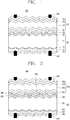
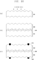
- FIG. 1 is a conceptual view illustrating an embodiment of a tandem solar cell 100 of the present disclosure.
- the tandem solar cell 100 includes a silicon solar cell 110, a junction layer 120, a perovskite solar cell 130, a lower electrode 140, and an upper electrode 150.
- the tandem solar cell 100 may be formed by sequentially stacking the lower electrode 140, the silicon solar cell 110, the junction layer 120, the perovskite solar cell 130, and the upper electrode 150.
- the silicon solar cell 110 may include a crystalline silicon substrate 111, a first conductive type semiconductor layer 112, a tunnel layer 113, and a second conductive type semiconductor layer 114.
- an anti-reflection film 115 may be disposed on a rear surface of the silicon solar cell 110.
- the anti-reflection film 115 is not necessarily provided, and may be omitted if necessary.
- the crystalline silicon substrate 111 may be formed of a second conductive type semiconductor layer.
- a carrier lifetime of the crystalline silicon substrate 111 can be improved due to a longer diffusion length than the first conductive type semiconductor layer containing a p-type impurity of the same or similar grade. This may further improve an efficiency of the silicon solar cell 110.
- a front surface and a rear surface of the crystalline silicon substrate 111 may be textured to have an unevenness.
- the unevenness is formed on a surface of the crystalline silicon substrate 111 and has pyramid shapes with irregular sizes, thereby reducing reflectance of incident light and increasing light conversion efficiency in a photoelectric transducer including an amorphous semiconductor layer.
- the first conductive type semiconductor layer 112, the tunnel layer 113, and the second conductive type semiconductor layer 114 formed on the front surface or the rear surface of the crystalline silicon substrate 111 having the textured uneven surface may also have uneven surfaces.
- the front surface and rear surface of the crystalline silicon substrate 111 are not limited to the uneven surface, and may be processed flat if necessary, or may have a rounded surface partially etched by an additional process. This may be appropriately adjusted so that the first conductive type semiconductor layer 112, the tunnel layer 113, and the second conductive type semiconductor layer 114 are stably formed on the front surface or the rear surface of the crystalline silicon substrate 111.
- the first conductive type semiconductor layer 112 forms an emitter on the front surface of the crystalline silicon substrate 111 to form a p-n junction. Furthermore, the first conductive type semiconductor layer 112 may be hydrogen passivated to prevent recombination of carriers.
- the second conductive type semiconductor layer 114 has a conductive type same as that of the crystalline silicon substrate 111 and forms a back surface field (BSF) having a higher impurity concentration than the crystalline silicon substrate 111.
- BSF back surface field
- the tunnel layer 113 is formed between the crystalline silicon substrate 111 and the second conductive type semiconductor layer 114 to allow selective collection of carriers.
- the tunnel layer 113 prevents movement of holes toward the second conductive type semiconductor layer 114 forming a back surface field, and facilitates movement of electrons. Accordingly, loss of carriers due to recombination at the rear surface of the crystalline silicon substrate 111 may be reduced.
- the tunnel layer 113 since the tunnel layer 113 moves carriers, the tunnel layer should have a thickness for an optimum probability of tunneling, and the thickness of the tunnel layer 113 for the optimum probability of tunneling may be in a range of 3 to 15 ⁇ in the present disclosure. Since the tunnel layer 113 has a thin thickness, it is difficult to uniformly form the surface of the tunnel layer 113 when the surface of the tunnel layer 113 is excessively curved. Accordingly, the textured uneven surface of the rear surface of the crystalline silicon substrate 111 may be processed flat or may be rounded by partially etching the textured uneven surface as shown in the drawing. In other words, the surface of the crystalline silicon substrate 111 on which the tunnel layer 113 is formed has a surface morphology suitable for forming the tunnel layer 113.
- the second conductive type semiconductor layer 114 may include polycrystalline silicon. Accordingly, the second conductive type semiconductor layer 114 may be deposited through low-pressure chemical vapor deposition to easily form a back surface field on the tunnel layer 113, and may be formed by implanting second conductive type impurities. For example, the second conductive type semiconductor layer 114 may be formed by implanting impurities of a pentavalent element such as phosphoryl chloride (POCI 3) or phosphoric acid (H 3 PO 4) into polycrystalline silicon.
- a pentavalent element such as phosphoryl chloride (POCI 3) or phosphoric acid (H 3 PO 4)
- the anti-reflection film 115 may be formed on a rear surface of the second conductive type semiconductor layer 114.
- the anti-reflection film 115 may serve to minimize reflection of light incident on the rear surface of the silicon solar cell 110.
- the anti-reflection film 115 may be formed by various processes such as physical vapor deposition (PECVD) or chemical vapor deposition (CVD). Further, the anti-reflection film 115 may be formed in a single layer or multi-layered structure including at least one selected from aluminum oxide (AlOx), silicon nitride (SiNx), silicon oxide (SiOx), and silicon oxynitride (SiOxNy).
- the lower electrode 140 may be formed of a material in which electrons formed in the tandem solar cell is easily moved by being brought into contact with the second conductive type semiconductor layer 114.
- the lower electrode 140 may be formed of conductive material of at least one selected from nickel (Ni), copper (Cu), silver (Ag), aluminum (Al), tin (Sn), zinc (Zn), indium (In), titanium (Ti), gold (Au), and a group consisting of combinations thereof, or other conductive metal materials.
- the lower electrode 140 may be formed by various methods such as screen printing using a metal paste, plating, thermal evaporation, and sputtering.
- the perovskite solar cell 130 and the upper electrode 150 disposed on a front surface of the junction layer 120 will be described.
- the perovskite solar cell 130 may be formed by sequentially stacking an electron transport layer 131, a perovskite absorption layer 132, a hole transport layer 133, and a transparent conductive oxide electrode layer 134 on the front surface of the junction layer 120.
- the silicon solar cell 110 of the tandem solar cell 100 is designed as a solar cell in which holes are moved to the front surface and electrons are moved to the rear surface of the silicon solar cell 110 to form electric energy. Accordingly, the hole transport layer 133 is formed on a front surface of the perovskite solar cell 130 and the electron transport layer 131 is formed on a rear surface of the perovskite solar cell 130 to implement a monolithic tandem solar cell. In another embodiment, when the solar cell is designed to form electric energy in a manner that electrons are moved to the front surface and holes are moved to the rear surface as opposed to the silicon solar cell 100, positions of the electron transport layer and the hole transport layer of the perovskite solar cell may be interchanged as needed.
- the electron transport layer 131 formed on the front surface of the junction layer 120 may be formed of a transparent conductive oxide (TCO) with high electrical conductivity, or a carbonaceous conductive material.
- TCO transparent conductive oxide
- the transparent conductive oxide implementing the electron transport layer 131 may be Ti oxide, Zn oxide, In oxide, Sn oxide, W oxide, Nb oxide, Mo oxide, Mg oxide, Zr oxide, Sr oxide, Yr oxide, La oxide, V oxide, Al oxide, Y oxide, Sc oxide, Sm oxide, Ga oxide, In oxide, SrTi oxide or the like.
- the electron transport layer 131 may include at least one selected from ZnO, TiO 2, SnO 2, WO 3, and TiSrO 3.
- graphene, carbon nanotubes, or fullerene (C 60) may be used as the carbonaceous conductive material.
- hole-electron pairs generated by receiving light energy from the sun may be decomposed into electrons or holes.
- electrons formed in the perovskite absorption layer 132 may be transferred to the electron transport layer 131, and holes formed in the perovskite absorption layer 132 may be transferred to the hole transport layer 133.
- the perovskite absorption layer 132 may contain an organic halide perovskite such as methyl ammonium iodide (MAI), and formamidinium iodide (FAI), or a metal halide perovskite such as lead iodide (Pbl 2), bromine iodide (PbBr), and lead chloride (PbCI 2).
- an organic halide perovskite such as methyl ammonium iodide (MAI), and formamidinium iodide (FAI)
- a metal halide perovskite such as lead iodide (Pbl 2), bromine iodide (PbBr), and lead chloride (PbCI 2).
- the perovskite absorption layer 132 may have a multilayered structure including at least one of organic halide perovskite and metal halide perovskite.
- the perovskite absorption layer 132 may be expressed as AMX 3 (where A is a monovalent organic ammonium cation or metal cation; M is a divalent metal cation; and X is a halogen anion).
- the perovskite absorption layer 132 may be formed by a single-step spin-coating method, a multi-step spin-coating method, a dual-source vapor deposition method, and a vapor-assisted solution process.
- the hole transport layer 133 may be formed of conductive polymer.
- conductive polymer polyaniline, polypyrrole, polythiophene, poly-3,4-ethylenedioxythiophene polystyrene sulfonate (PEDOT-PSS), poly-[bis(4-phenyl)(2,4,6) -Trimethylphenyl)amine] (PTAA), Spiro-MeOTAD, or polyaniline-camposulfonic acid (PANI-CSA), and the like may be used.
- the conductive oxide electrode layer 134 may be implemented as a transparent conductive oxide (TCO) with high electrical conductivity. Furthermore, the upper electrode 150 may be formed of a material having higher electrical conductivity than the conductive oxide electrode layer 134, thereby improving carrier collection efficiency and reducing resistance.
- TCO transparent conductive oxide
- the perovskite absorption layer 132 may be deteriorated due to the heat. Accordingly, the upper electrode 150 may be formed by screen printing using a low-temperature paste which does not contain glass frit and can be easily sintered even at a low temperature. Furthermore, the perovskite absorption layer 132 may be formed by various methods such as plating, thermal evaporation, and sputtering in a temperature range in which the perovskite absorption layer 132 is not deteriorated.
- a front anti-reflection film (not illustrated) may be further provided on the front surface of the perovskite solar cell 130.
- the front anti-reflection film may be stacked on an exposed front surface of the conductive oxide electrode layer 134 and on a front surface of the upper electrode 150.
- the front anti-reflection film may be formed in a single layer or multi-layered structure including at least one selected from magnesium fluoride (MgF 2), silicon oxide (SiOx), and titanium oxide (TiOx). This may effectively reduce surface reflectance of the tandem solar cell 100, thereby improving light conversion efficiency of the tandem solar cell.
- FIGS. 2 to 8 are conceptual views illustrating various embodiments of tandem solar cells 200, 300, 400, 500, 600, 700, and 800 of the present disclosure.
- tandem solar cells 200, 300, 400, 500, 600, 700, and 800 of the present disclosure will be described with reference to FIGS. 2 to 8 .
- the same or similar reference numerals are designated to the same or similar configurations to FIG. 1 , and the description thereof will be substituted by the earlier description.
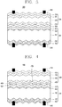
- a tandem solar cell 200 includes a silicon solar cell 210, a junction layer 220, a perovskite solar cell 230, a lower electrode 240, and an upper electrode 250.
- the tandem solar cell 200 is provided with a hydrogen ion supply layer 260 between the junction layer 220 and a first conductive type semiconductor layer 212 disposed on a front surface of the silicon solar cell 210.
- an anti-reflection film 215 may be disposed on a rear surface of the silicon solar cell 200.
- the hydrogen ion supply layer 260 may be formed by supplying hydrogen from an insulating film rich in hydrogen.
- the hydrogen ion supply layer 260 may be formed of hydrogenated silicon nitride (SiNx). Accordingly, hydrogen is supplied to the first conductive type semiconductor layer 212, and therefore, the first conductive type semiconductor layer 212 is hydrogen passivated to reduce surface defects.
- the hydrogen ion supply layer 260 may be patterned to have an opening 270 through which a portion of the first conductive type semiconductor layer 212 is exposed.
- the first conductive type semiconductor layer 212 disposed on the opening 270 may be recrystallized.
- the opening 270 may be filled with the junction layer 220. Accordingly, the first conductive type semiconductor layer 212 is brought into contact with the junction layer 220 to allow electrons formed in the perovskite solar cell 230 to move to the silicon solar cell 210, and to allow holes formed in the silicon solar cell 210 to move to the perovskite solar cell 230.
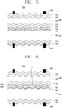
- a silicon solar cell 310, 410 may be formed by sequentially stacking a first conductive type semiconductor layer 312, 412, a crystalline silicon substrate 311, 411, a tunnel layer 313, 413, and a second conductive type semiconductor layer 314, 414 on a front surface of a lower electrode 340, 440.
- the crystalline silicon substrate 311, 411 contains second conductive type impurities.
- the second conductive type semiconductor layer 314, 414 is formed of polycrystalline silicon.
- an anti-reflection film 315, 415 may be disposed on a rear surface of the silicon solar cell 310, 410.
- the silicon solar cell 310, 410 has a rear emitter structure in which a p-n junction is formed by including the first conductive type semiconductor layer 312, 412 on the rear surface of the silicon solar cell 310, 410.
- the first conductive type semiconductor layer 312, 412 may be hydrogen passivated by receiving hydrogen ions from the anti-reflection film 315, 415 disposed on a rear surface of the first conductive type semiconductor layer 312, 412.
- the silicon solar cell 310, 410 forms a structure having a front surface field (FSF) on the front surface of the silicon solar cell 310, 410. Accordingly, the silicon solar cell 310, 410 may be designed to form electric energy by electrons being moved to the front surface of the silicon solar cell 310, 410 and holes being moved to the rear surface of the silicon solar cell 310, 410.
- FSF front surface field
- an electron transport layer 331, 431 and a hole transport layer 333, 433 of a perovskite solar cell 330, 430 may be formed in an arrangement opposite to the arrangement in FIGS. 1 and 2 described above.
- the electron transport layer 331, 431 is disposed on a front surface of the perovskite solar cell 330, 430
- the hole transport layer 333, 433 is disposed on a rear surface of the perovskite solar cell 330, 430 to implement a tandem solar cell.
- the tandem solar cell 400 may be provided with a hydrogen ion supply layer 460 and an opening 470, between a junction layer 420 and a second conductive type semiconductor layer 414 disposed on a front surface of the silicon solar cell 410.
- the second conductive type semiconductor layer 414 disposed on the opening 470 may be recrystallized.
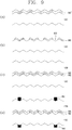
- first conductive type semiconductor layers 512, 612, 712, and 812 of solar cells 500, 600, 700, and 800 may be formed of polycrystalline silicon.
- second conductive type semiconductor layers 114, 214, 314, and 414 are formed of polycrystalline silicon. Accordingly, the second conductive type semiconductor layers 114, 214, 314, and 414 formed of polycrystalline silicon in FIGS. 1 to 4 each forms a front surface field or a back surface field.
- the first conductive type semiconductor layers 512, 612, 712, and 812 formed of polycrystalline silicon of FIGS. 5 to 8 each may form an emitter.
- the first conductive type semiconductor layer 512, 612, 712, 812 may be deposited through low-pressure chemical vapor deposition to easily form a back surface field on a tunnel layer 513, 613, 713, 813, and may be formed by implanting a first conductive type impurity.
- the first conductive type semiconductor layer 512, 612, 712, 812 may be formed by implanting an impurity of a trivalent element such as diborane (B 2H 6) or boron tribromide (BBr 3) into polycrystalline silicon.
- the first conductive type semiconductor layer 512, 612 is formed of polycrystalline silicon, and a silicon solar cell 510, 610 may be formed by sequentially stacking a second conductive type semiconductor layer 514, 614, a crystalline silicon substrate 511, 611, a tunnel layer 513, 613, and a first conductive type semiconductor layer 512, 612 on a front surface of a lower electrode 540, 640.
- the crystalline silicon substrate 511, 611 contains second conductive type impurities.
- the second conductive type semiconductor layer 514, 614 may be hydrogen passivated by receiving hydrogen ions from an anti-reflection film 515, 615 disposed on a rear surface of the second conductive type semiconductor layer 514, 614 to reduce surface defects.
- the silicon solar cell 510, 610 a p-n junction is formed by bonding the first conductive type semiconductor layer 512, 612 formed of polycrystalline silicon with the crystalline silicon substrate 511, 611. Accordingly, the silicon solar cell 510, 610 may be designed to form electric energy by holes being moved to the front surface of the silicon solar cell 510, 610 and electrons being moved to the rear surface of the silicon solar cell 510, 610.
- a perovskite solar cell 530, 630 of the tandem solar cell 500, 600 may be formed by sequentially stacking an electron transport layer 531, 631, a perovskite absorption layer 532, 632, a hole transport layer 533, 633, and a transparent conductive oxide electrode layer 534, 634 on a front surface of a junction layer 520, 620.
- the tandem solar cell 600 may be provided with a hydrogen ion supply layer 660 and an opening 670, between the junction layer 620 and a first conductive type semiconductor layer 612 disposed on a front surface of the silicon solar cell 610.
- the first conductive type semiconductor layer 612 disposed on the opening 670 may be recrystallized.
- a silicon solar cell 710, 810 may be formed by sequentially stacking a first conductive type semiconductor layer 712, 812, a tunnel layer 713, 813, a crystalline silicon substrate 711, 811, and a second conductive type semiconductor layer 714, 814 on a front surface of a lower electrode 740, 840.
- the crystalline silicon substrate 711, 811 contains second conductive type impurities.
- the first conductive type semiconductor layer 712, 812 is formed of polycrystalline silicon.
- an anti-reflection film 715, 815 may be disposed on a rear surface of the silicon solar cell 710, 810.
- the silicon solar cell 710, 810 has a rear emitter structure in which a p-n junction is formed by including the first conductive type semiconductor layer 712, 812 on the rear surface of the silicon solar cell 710, 810. Meanwhile, the silicon solar cell 710, 810 forms a structure having a front surface field (FSF) on the front surface of the silicon solar cell 710, 810 by the second conductive type semiconductor layer 714, 814. Accordingly, the silicon solar cell 710, 810 may be designed to form electric energy by electrons being moved to the front surface of the silicon solar cell 710, 810 and holes being moved to the rear surface of the silicon solar cell 710, 810.
- FSF front surface field
- a perovskite solar cell 730, 830 is formed by sequentially stacking a hole transport layer 733, 833, a perovskite absorption layer 732, 832, an electron transport layer 731, 831, and a transparent conductive oxide electrode layer 734, 834 on a front surface of a junction layer 720, 820. Accordingly, the silicon solar cell 710, 810 and the perovskite solar cell 730, 830 form a tandem solar cell.
- the tandem solar cell 800 may be provided with a hydrogen ion supply layer 860 and an opening 870, between the junction layer 820 and a second conductive type semiconductor layer 814 disposed on a front surface of the silicon solar cell 810.
- the second conductive type semiconductor layer 814 disposed on the opening 870 may be recrystallized.
- FIG. 9 is a conceptual view illustrating an embodiment of a method for manufacturing a tandem solar cell 900 of the present disclosure.
- a hydrogen ion supply layer 960' is stacked on a front surface of a silicon solar cell 910.
- a tunnel layer and a polycrystalline silicon layer are stacked on one surface of a crystalline silicon substrate.
- a first impurity implantation step of implanting a first conductive type impurity or a second conductive type impurity into the polycrystalline silicon layer is performed to form a first conductive type semiconductor layer or a second conductive type semiconductor layer.
- a step of second impurity implantation in which an impurity having a conductive type different from the impurity implanted in the step of the first impurity implantation is implanted into another surface of the crystalline silicon substrate, is performed.
- the silicon solar cell 910 including the crystalline silicon substrate, the tunnel layer, the first conductive type semiconductor layer, and the second conductive type semiconductor layer may be prepared.
- an anti-reflection film may be provided on a rear surface of the silicon solar cell 910.
- hydrogen is supplied to a surface of the first conductive type semiconductor layer or a surface of the second conductive type semiconductor layer formed on a front surface of the silicon solar cell 910 by the hydrogen ion supply layer 960' to thereby stabilize defects such as dangling bonds. Accordingly, the front surface of the silicon solar cell 910 may be hydrogen passivated to prevent recombination of carriers.
- a hydrogen ion supply layer 960 may be formed, and an opening 970 through which a portion of the first conductive type semiconductor layer or the second conductive type semiconductor layer formed on the front surface of the silicon solar cell 910 is exposed may be provided.
- the opening 970 allows a junction layer 920 which is to be stacked on the front surface of the silicon solar cell 910 and the silicon solar cell 910 to be electrically connected to each other.
- removal of the hydrogen ion supply layer 960' may be performed by laser patterning or chemical etching. Further, by removing the entire hydrogen ion supply layer 960', the first conductive type semiconductor layer or the second conductive type semiconductor layer formed on the front surface of the silicon solar cell 910 and the junction layer 920 may be electrically connected to each other.
- the hydrogen ion supply layer 960' may be patterned as described above when removing the hydrogen ion supply layer 960' by laser patterning, or the entire hydrogen ion supply layer 960' may be removed by laser patterning. Even in this case, although polycrystalline silicon is recrystallized during the laser patterning, it does not directly affect the decrease in the efficiency of the silicon solar cell 910.
- the junction layer 920 and a perovskite solar cell 930 are formed on the front surface of the silicon solar cell 910 on which the hydrogen ion supply layer 960 and the opening 970 are formed.
- the perovskite solar cell 930 is formed such that an electron transport layer, a perovskite absorption layer, a hole transport layer, and a transparent conductive oxide electrode layer are appropriately stacked on a front surface of the junction layer 920 according to a design of the silicon solar cell 910.
- a lower electrode 940 is formed on the rear surface of the silicon solar cell 910, and an upper electrode 950 is formed on a front surface of the perovskite solar cell 930 to manufacture the tandem solar cell 900.
- the lower electrode 940 and the upper electrode 950 may be sequentially formed.
- the lower electrode 940 on the rear surface of the silicon solar cell 910 may be provided first.
- the upper electrode 950 may be formed on the front surface of the perovskite solar cell 930.
- a front anti-reflection film may be provided on a surface where a transparent conductive oxide layer of the perovskite solar cell 930 is exposed and a front surface of the upper electrode.
- FIG. 10 is a conceptual view illustrating another embodiment of a method for manufacturing a tandem solar cell 1000 of the present disclosure.
- a surface of a first conductive type semiconductor layer or a surface of a second conductive type semiconductor layer formed on a front surface of a silicon solar cell 1010 may be exposed to a hydrogen plasma. Accordingly, hydrogen is supplied to the surface of the first conductive type semiconductor layer or the surface of the second conductive type semiconductor layer formed on the front surface of the silicon solar cell 910 to stabilize defects such as dangling bonds. Accordingly, the front surface of the silicon solar cell 1010 may be hydrogen passivated to prevent recombination of carriers.
- a junction layer 1020 and a perovskite solar cell 1030 are formed on a front surface of the silicon solar cell 1010.
- the perovskite solar cell 1030 is formed such that an electron transport layer, a perovskite absorption layer, a hole transport layer, and a transparent conductive oxide electrode layer are appropriately stacked on a front surface of the junction layer 1020 according to a design of the silicon solar cell 1010.
- a lower electrode 1040 is formed on a rear surface of the silicon solar cell 1010, and an upper electrode 1050 is formed on a front surface of the perovskite solar cell 1030 to manufacture the tandem solar cell 1000.
- the lower electrode 1040 and the upper electrode 1050 are formed after the perovskite solar cell 1030 is formed.
- the lower electrode 1040 may be provided after preparing the silicon solar cell 1010
- the upper electrode 1050 may be provided after the perovskite solar cell 1030 is formed, so that the lower electrode 1040 and the upper electrode 1050 are sequentially and separately formed.
- a front anti-reflection film may be provided on a surface where a transparent conductive oxide layer of the perovskite solar cell 1030 is exposed and a front surface of the upper electrode.
- the method for manufacturing the solar cell described above is not limited to the configurations and the methods of the embodiments described above, but the embodiments may be configured by selectively combining all or part of the embodiments so that various modifications or changes can be made.
Landscapes
- Engineering & Computer Science (AREA)
- Power Engineering (AREA)
- Microelectronics & Electronic Packaging (AREA)
- Electromagnetism (AREA)
- Physics & Mathematics (AREA)
- Computer Hardware Design (AREA)
- General Physics & Mathematics (AREA)
- Condensed Matter Physics & Semiconductors (AREA)
- Life Sciences & Earth Sciences (AREA)
- Sustainable Development (AREA)
- Chemical & Material Sciences (AREA)
- Sustainable Energy (AREA)
- Materials Engineering (AREA)
- Crystallography & Structural Chemistry (AREA)
- Electrochemistry (AREA)
- Chemical Kinetics & Catalysis (AREA)
- Manufacturing & Machinery (AREA)
- Inorganic Chemistry (AREA)
- Photovoltaic Devices (AREA)
Applications Claiming Priority (2)
| Application Number | Priority Date | Filing Date | Title |
|---|---|---|---|
| KR1020180164546A KR20200075640A (ko) | 2018-12-18 | 2018-12-18 | 텐덤 태양전지 |
| PCT/KR2019/014044 WO2020130318A1 (ko) | 2018-12-18 | 2019-10-24 | 텐덤 태양전지 |
Publications (2)
| Publication Number | Publication Date |
|---|---|
| EP3902019A1 true EP3902019A1 (de) | 2021-10-27 |
| EP3902019A4 EP3902019A4 (de) | 2022-08-03 |
Family
ID=71100335
Family Applications (1)
| Application Number | Title | Priority Date | Filing Date |
|---|---|---|---|
| EP19900237.9A Pending EP3902019A4 (de) | 2018-12-18 | 2019-10-24 | Tandemsolarzelle |
Country Status (4)
| Country | Link |
|---|---|
| US (2) | US11616160B2 (de) |
| EP (1) | EP3902019A4 (de) |
| KR (1) | KR20200075640A (de) |
| WO (1) | WO2020130318A1 (de) |
Families Citing this family (6)
| Publication number | Priority date | Publication date | Assignee | Title |
|---|---|---|---|---|
| KR102511845B1 (ko) * | 2020-08-13 | 2023-03-17 | 서울대학교산학협력단 | 와이드 밴드갭을 가지는 페로브스카이트 박막의 제조 방법, 이에 의해 제조된 페로브스카이트 박막, 이를 포함하는 태양전지 |
| CN113707647B (zh) * | 2021-11-01 | 2022-01-28 | 南京日托光伏新能源有限公司 | 一种钙钛矿/mwt异质结串并联复合电池的制备方法 |
| CN114447025A (zh) * | 2022-01-06 | 2022-05-06 | 青海黄河上游水电开发有限责任公司光伏产业技术分公司 | 一种叠层钙钛矿太阳能电池及其制作方法 |
| WO2023147338A2 (en) * | 2022-01-28 | 2023-08-03 | The University Of North Carolina At Chapel Hill | Defect engineering in wide bandgap perovskites for efficient and stable fully textured perovskite-silicon tandem solar cells |
| KR102653820B1 (ko) | 2022-02-22 | 2024-04-01 | 한화솔루션 주식회사 | 탠덤형 페로브스카이트 태양전지 모듈의 제조방법 |
| KR20230149924A (ko) | 2022-04-21 | 2023-10-30 | 한화솔루션 주식회사 | 탠덤형 페로브스카이트 태양전지 하프셀의 제조방법 |
Family Cites Families (16)
| Publication number | Priority date | Publication date | Assignee | Title |
|---|---|---|---|---|
| JPS58203233A (ja) * | 1982-05-21 | 1983-11-26 | Iseki & Co Ltd | Ptoクラツチの作動油圧制御装置 |
| US6677214B1 (en) * | 1993-11-19 | 2004-01-13 | Mega Chips Corporation | Semiconductor device and method of fabricating the same |
| US5738731A (en) * | 1993-11-19 | 1998-04-14 | Mega Chips Corporation | Photovoltaic device |
| DE102007012277A1 (de) * | 2007-03-08 | 2008-09-11 | Gebr. Schmid Gmbh & Co. | Verfahren zur Herstellung einer Solarzelle sowie damit hergestellte Solarzelle |
| CN105493304B (zh) * | 2013-08-06 | 2020-01-31 | 新南创新私人有限公司 | 高效堆叠的太阳能电池 |
| JP6188921B2 (ja) * | 2014-03-31 | 2017-08-30 | 国立研究開発法人科学技術振興機構 | 太陽電池および太陽電池の製造方法 |
| US20160019037A1 (en) | 2014-07-21 | 2016-01-21 | Xamarin Inc. | Managing parameter types for generic functions |
| CN107431128B (zh) * | 2015-01-08 | 2020-12-25 | 韩国化学研究院 | 包括有机、无机杂化钙钛矿化合物膜的器件的制备方法及包括有机、无机杂化钙钛矿化合物膜的器件 |
| KR101626248B1 (ko) * | 2015-01-09 | 2016-05-31 | 고려대학교 산학협력단 | 실리콘 태양전지 및 이의 제조 방법 |
| MY190432A (en) | 2015-06-12 | 2022-04-21 | Oxford Photovoltaics Ltd | Multijunction photovoltaic device |
| WO2017105248A1 (en) * | 2015-12-18 | 2017-06-22 | Stichting Energieonderzoek Centrum Nederland | Hybrid tandem solar cell |
| NL2015987B1 (en) * | 2015-12-18 | 2017-07-10 | Stichting Energieonderzoek Centrum Nederland | Tandem solar cell and method for manufacturing such a solar cell. |
| WO2017163498A1 (ja) | 2016-03-23 | 2017-09-28 | 三菱電機株式会社 | 太陽電池、および、太陽電池の製造方法 |
| KR101823597B1 (ko) * | 2016-07-21 | 2018-01-30 | 엘지전자 주식회사 | 태양전지 및 그 제조 방법 |
| KR102457929B1 (ko) * | 2016-12-02 | 2022-10-25 | 상라오 징코 솔라 테크놀러지 디벨롭먼트 컴퍼니, 리미티드 | 텐덤 태양전지 및 그 제조 방법 |
| EP3331029B1 (de) * | 2016-12-02 | 2021-09-01 | LG Electronics Inc. | Tandemsolarzelle und verfahren zur herstellung davon |
-
2018
- 2018-12-18 KR KR1020180164546A patent/KR20200075640A/ko not_active Application Discontinuation
-
2019
- 2019-10-24 EP EP19900237.9A patent/EP3902019A4/de active Pending
- 2019-10-24 US US17/414,223 patent/US11616160B2/en active Active
- 2019-10-24 WO PCT/KR2019/014044 patent/WO2020130318A1/ko unknown
-
2023
- 2023-01-05 US US18/150,270 patent/US11830958B2/en active Active
Also Published As
| Publication number | Publication date |
|---|---|
| US20220209039A1 (en) | 2022-06-30 |
| WO2020130318A1 (ko) | 2020-06-25 |
| EP3902019A4 (de) | 2022-08-03 |
| US20230163228A1 (en) | 2023-05-25 |
| US11830958B2 (en) | 2023-11-28 |
| US11616160B2 (en) | 2023-03-28 |
| KR20200075640A (ko) | 2020-06-26 |
Similar Documents
| Publication | Publication Date | Title |
|---|---|---|
| US11830958B2 (en) | Tandem solar cell | |
| USRE47484E1 (en) | Solar cell | |
| CN107634119B (zh) | 串联太阳能电池及包括其的串联太阳能电池模块 | |
| US9972738B2 (en) | Solar cell and method for manufacturing the same | |
| EP2434548B1 (de) | Solarzelle und Verfahren zu ihrer Herstellung | |
| US20170170340A1 (en) | Solar cell | |
| EP2804219B1 (de) | Solarzelle und verfahren zu ihrer herstellung | |
| CN115241298B (zh) | 太阳能电池及其制备方法、光伏组件 | |
| US20100218818A1 (en) | Solar cell and method of manufacturing the same | |
| KR102367784B1 (ko) | 텐덤 태양전지, 이를 포함하는 텐덤 태양전지 모듈 및 이의 제조방법 | |
| US9640673B2 (en) | Solar cell and manufacturing method thereof | |
| US20130160840A1 (en) | Solar cell | |
| US20130125964A1 (en) | Solar cell and manufacturing method thereof | |
| KR100990864B1 (ko) | 태양전지 및 그 제조 방법 | |
| KR102586115B1 (ko) | 양면 수광형 실리콘 태양전지 | |
| KR20180063866A (ko) | 텐덤 태양전지 및 그 제조 방법 | |
| EP2903037B1 (de) | Herstellungsverfahren für rückseitig kontakierte Solarzelle mit Heteroübergang | |
| KR101882439B1 (ko) | 태양 전지 및 그 제조 방법 | |
| US20110094586A1 (en) | Solar cell and method for manufacturing the same | |
| KR20200061479A (ko) | 전하선택 박막을 포함하는 실리콘 태양전지 및 이의 제조방법 | |
| CN114695583B (zh) | 太阳电池及生产方法、光伏组件 | |
| JP7248856B1 (ja) | 太陽電池および太陽電池の製造方法、光起電力モジュール | |
| KR20150109745A (ko) | 태양 전지 및 이의 제조 방법 | |
| KR20180036504A (ko) | 태양 전지 및 태양 전지 제조 방법 |
Legal Events
| Date | Code | Title | Description |
|---|---|---|---|
| STAA | Information on the status of an ep patent application or granted ep patent |
Free format text: STATUS: THE INTERNATIONAL PUBLICATION HAS BEEN MADE |
|
| PUAI | Public reference made under article 153(3) epc to a published international application that has entered the european phase |
Free format text: ORIGINAL CODE: 0009012 |
|
| STAA | Information on the status of an ep patent application or granted ep patent |
Free format text: STATUS: REQUEST FOR EXAMINATION WAS MADE |
|
| 17P | Request for examination filed |
Effective date: 20210621 |
|
| AK | Designated contracting states |
Kind code of ref document: A1 Designated state(s): AL AT BE BG CH CY CZ DE DK EE ES FI FR GB GR HR HU IE IS IT LI LT LU LV MC MK MT NL NO PL PT RO RS SE SI SK SM TR |
|
| DAV | Request for validation of the european patent (deleted) | ||
| DAX | Request for extension of the european patent (deleted) | ||
| REG | Reference to a national code |
Ref country code: DE Ref legal event code: R079 Free format text: PREVIOUS MAIN CLASS: H01L0031072500 Ipc: H01L0031043000 |
|
| A4 | Supplementary search report drawn up and despatched |
Effective date: 20220705 |
|
| RIC1 | Information provided on ipc code assigned before grant |
Ipc: H01L 51/42 20060101ALI20220629BHEP Ipc: H01L 31/18 20060101ALI20220629BHEP Ipc: H01L 31/0745 20120101ALI20220629BHEP Ipc: H01L 31/078 20120101ALI20220629BHEP Ipc: H01L 31/043 20140101AFI20220629BHEP |
|
| RAP1 | Party data changed (applicant data changed or rights of an application transferred) |
Owner name: SHANGRAO JINKO SOLAR TECHNOLOGY DEVELOPMENT CO., LTD |
|
| RAP1 | Party data changed (applicant data changed or rights of an application transferred) |
Owner name: SHANGRAO JINKO SOLAR TECHNOLOGY DEVELOPMENT CO., LTD |
|
| RAP3 | Party data changed (applicant data changed or rights of an application transferred) |
Owner name: SHANGRAO XINYUAN YUEDONG TECHNOLOGY DEVELOPMENT CO. LTD |
|
| RAP1 | Party data changed (applicant data changed or rights of an application transferred) |
Owner name: TRINA SOLAR CO., LTD |