EP3896838B1 - Vibration power generation element - Google Patents
Vibration power generation element Download PDFInfo
- Publication number
- EP3896838B1 EP3896838B1 EP20744736.8A EP20744736A EP3896838B1 EP 3896838 B1 EP3896838 B1 EP 3896838B1 EP 20744736 A EP20744736 A EP 20744736A EP 3896838 B1 EP3896838 B1 EP 3896838B1
- Authority
- EP
- European Patent Office
- Prior art keywords
- layer
- moveable
- elastically
- electrode
- vibration
- Prior art date
- Legal status (The legal status is an assumption and is not a legal conclusion. Google has not performed a legal analysis and makes no representation as to the accuracy of the status listed.)
- Active
Links
- 238000010248 power generation Methods 0.000 title description 4
- 238000003306 harvesting Methods 0.000 claims description 66
- 239000000758 substrate Substances 0.000 claims description 24
- 238000009413 insulation Methods 0.000 claims description 15
- 238000003780 insertion Methods 0.000 claims description 3
- 230000037431 insertion Effects 0.000 claims description 3
- 238000005530 etching Methods 0.000 description 14
- 230000000052 comparative effect Effects 0.000 description 8
- 229910021420 polycrystalline silicon Inorganic materials 0.000 description 8
- 238000000034 method Methods 0.000 description 7
- 238000001020 plasma etching Methods 0.000 description 7
- VYPSYNLAJGMNEJ-UHFFFAOYSA-N Silicium dioxide Chemical compound O=[Si]=O VYPSYNLAJGMNEJ-UHFFFAOYSA-N 0.000 description 6
- 229910052681 coesite Inorganic materials 0.000 description 3
- 229910052906 cristobalite Inorganic materials 0.000 description 3
- 230000000694 effects Effects 0.000 description 3
- 239000012212 insulator Substances 0.000 description 3
- 229910052751 metal Inorganic materials 0.000 description 3
- 239000002184 metal Substances 0.000 description 3
- 229910052710 silicon Inorganic materials 0.000 description 3
- 239000010703 silicon Substances 0.000 description 3
- 239000000377 silicon dioxide Substances 0.000 description 3
- 229910052682 stishovite Inorganic materials 0.000 description 3
- 229910052905 tridymite Inorganic materials 0.000 description 3
- KRHYYFGTRYWZRS-UHFFFAOYSA-N Fluorane Chemical compound F KRHYYFGTRYWZRS-UHFFFAOYSA-N 0.000 description 2
- 229910052782 aluminium Inorganic materials 0.000 description 2
- XAGFODPZIPBFFR-UHFFFAOYSA-N aluminium Chemical compound [Al] XAGFODPZIPBFFR-UHFFFAOYSA-N 0.000 description 2
- 230000005611 electricity Effects 0.000 description 2
- 238000005516 engineering process Methods 0.000 description 2
- -1 Sulfuric acid Peroxide Chemical class 0.000 description 1
- 238000004140 cleaning Methods 0.000 description 1
- 238000004891 communication Methods 0.000 description 1
- 230000007423 decrease Effects 0.000 description 1
- 238000004519 manufacturing process Methods 0.000 description 1
- 239000000203 mixture Substances 0.000 description 1
- 230000007935 neutral effect Effects 0.000 description 1
- 230000000414 obstructive effect Effects 0.000 description 1
- 229910001414 potassium ion Inorganic materials 0.000 description 1
- 230000000452 restraining effect Effects 0.000 description 1
- 238000005549 size reduction Methods 0.000 description 1
- QAOWNCQODCNURD-UHFFFAOYSA-N sulfuric acid Substances OS(O)(=O)=O QAOWNCQODCNURD-UHFFFAOYSA-N 0.000 description 1
- 238000001039 wet etching Methods 0.000 description 1
Images


Classifications
-
- H—ELECTRICITY
- H02—GENERATION; CONVERSION OR DISTRIBUTION OF ELECTRIC POWER
- H02N—ELECTRIC MACHINES NOT OTHERWISE PROVIDED FOR
- H02N1/00—Electrostatic generators or motors using a solid moving electrostatic charge carrier
- H02N1/06—Influence generators
- H02N1/08—Influence generators with conductive charge carrier, i.e. capacitor machines
Definitions
- the present invention relates to a vibration-driven energy harvesting element.
- a very small vibration-driven energy harvesting element has been developed by using a MEMS technology.
- a moveable electrode portion on which a comb electrode is formed is made to vibrate with respect to a fixed portion on which a comb electrode is formed to generate electricity.
- a vibration-driven energy harvesting element described in Patent Literature 1 a fixed portion, a moveable portion, and a support beam portion that elastically supports the moveable portion are formed in one layer of an SOI (Silicon On Insulator) substrate of 3-layers structure, and change in capacitance is used to generate electricity when the moveable portion is vibrated with respect to the fixed portion.
- SOI Silicon On Insulator
- Patent Literature 1 Japanese Patent No. 6338070
- One way of increasing the amount of power generation while restraining increase in the size of the vibration-driven energy harvesting element is to enhance change in capacitance by increasing the area ratio of the fixed portion and the moveable portion in the vibration-driven energy harvesting element.
- the vibration-driven energy harvesting element described in Patent Literature 1 requires an area for arranging the support beam portion, and the support beam portion has been an obstructive factor for increasing the area ratio of the fixed portion and the moveable portion.
- a problem has been that the size of the vibration-driven energy harvesting element is increased by the area for the support beam portion.
- a vibration-driven energy harvesting element includes: a fixed electrode portion and a moveable electrode portion formed in a second layer of a substrate provided with a first layer and the second layer with an insulation layer interposed therebetween; a frame body formed from the first layer and the second layer disposed with the insulation layer interposed therebetween, the frame body supporting the fixed electrode portion in the second layer; an elastically-supporting portion formed in the first layer and elastically supporting the moveable electrode portion by a beam portion joined to the first layer of the frame body; and a first conduction portion electrically connecting the moveable electrode portion and the elastically-supporting portion.
- the first conduction portion includes a first plate-like member formed in the second layer that is continuous with the moveable electrode portion and facing the elastically-supporting portion without the insulation layer interposed therebetween, the first plate-like member has: a first deforming portion in a cantilevered shape facing the elastically-supporting portion without the insulation layer interposed therebetween; and a first attaching portion connected to a distal end of the first deforming portion in a cantilevered shape and extending from the distal end in a folding back manner in a root direction of the first deforming portion, the first attaching portion being attached to the elastically-supporting portion, and the first deforming portion and the first attaching portion have a plurality of holes formed therein, the holes passing through in a thickness direction of the first plate-like member.
- a second conduction portion electrically connecting the first layer and the second layer of the frame body is included.
- the second conduction portion includes a second plate-like member formed in the second layer of the frame body and facing the first layer of the frame body without the insulation layer interposed therebetween, the second plate-like member has: a second deforming portion in a cantilevered shape facing the first layer of the frame body without the insulation layer interposed therebetween; and a second attaching portion connected to a distal end of the second deforming portion in a cantilevered shape and extending from the distal end in a folding back manner in a root direction of the second deforming portion, the second attaching portion being attached to the first layer of the frame body, and the second deforming portion and the second attaching portion have a plurality of holes formed therein, the holes passing through in a thickness direction of the second plate-like member.
- the fixed electrode portion has a plurality of fixed comb teeth
- the moveable electrode portion has a plurality of moveable comb teeth arranged to interdigitate with the plurality of fixed comb teeth with a gap interposed therebetween
- the elastically-supporting portion elastically supports the moveable electrode portion so as to be displaceable in a direction in which an amount of insertion of the moveable comb teeth relative to the fixed comb teeth changes.
- a vibration-driven energy harvesting element includes: a fixed comb electrode formed in a first layer of a substrate including the first layer and a second layer layered with an insulation layer interposed therebetween; a moveable comb electrode formed in the first layer and moveable relative to the fixed comb electrode; an elastically-supporting portion formed in the second layer and elastically supporting the moveable comb electrode; and a connecting portion formed in the first layer and mechanically and electrically connecting the moveable comb electrode to the elastically-supporting portion.
- the size of the vibration-driven energy harvesting element can be reduced.
- FIG. 1 is a plan view illustrating an example of a vibration-driven energy harvesting element 1.
- the vibration-driven energy harvesting element 1 is formed by using an SOI (Silicon On Insulator) substrate and through a general MEMS processing technology.
- the SOI substrate is a substrate of 3-layers structure composed of a handle layer 2A made of Si, a BOX layer 2B made of SiO 2 , and a device layer 2C made of Si.
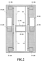
- Figure 2 illustrates shapes of the handle layer 2A and the BOX layer 2B in the vibration-driven energy harvesting element 1.
- the vibration-driven energy harvesting element 1 includes a frame body 10 in a frame shape, 4 sets of fixed electrode portions 11 fixed to the frame body 10, a moveable electrode portion 12, a part of which is paired with one of the fixed electrode portions 11, an elastically-supporting portion 13 elastically supporting the moveable electrode portion 12, and a conduction portion 15 mechanically and electrically connecting the moveable electrode portion 12 to the elastically-supporting portion 13.
- the device layer 2C is provided on a front face side as illustrated, the 4 sets of fixed electrode portions 11 and the moveable electrode portion 12 are formed in the device layer 2C, and the elastically-supporting portion 13 is formed in the handle layer 2A on a back face side.
- the frame body 10 is formed from the handle layer 2A and the device layer 2C disposed with the BOX layer 2B interposed therebetween.
- conduction portions 14, which mechanically and electrically connect the device layer 2C on the front face side and the handle layer 2A on the back face side, are formed at two locations.
- the conduction portion 15 is formed in a similar manner in the center of the moveable electrode portion 12.
- Each of the fixed electrode portions 11 is provided with an electrode pad 111, and each of the conduction portion 14 is also provided with an electrode pad 145.
- the elastically-supporting portion 13 is formed in the handle layer 2A.
- the elastically-supporting portion 13 includes a moveable electrode joint portion 130 disposed with the moveable electrode portion 12 being joined thereto, the moveable electrode portion 12 being formed in the device layer 2C, and 4 sets of beam portions 131 elastically supporting the moveable electrode joint portion 130 on the frame body 10 formed in the handle layer 2A.
- the conduction portion 15 in the device layer 2C illustrated in Figure 1 is electrically connected to the moveable electrode joint portion 130 in the handle layer 2A with a deforming portion 151 interposed therebetween, which will be described later.
- the moveable electrode portion 12 on the front face side of the SOI substrate is electrically continuous with the moveable electrode joint portion 130 on the back face side of the SOI substrate with the conduction portion 15 interposed therebetween.
- the frame body 10 is in a rectangular frame shape, and the 4 sets of beam portions 131 of the elastically-supporting portion 13 in the handle layer 2A are joined to the handle layer 2A of the frame body 10.
- the moveable electrode portion 12 in the device layer 2C is joined to the moveable electrode joint portion 130 in the handle layer 2A with the deforming portion 151 of the conduction portion 15 in the device layer 2C interposed therebetween, and the moveable electrode joint portion 130 is elastically supported in the handle layer 2A of the frame body 10 by the beam 131.
- a hatched area S0 in Figure 2 indicates the BOX layer 2B between the handle layer 2A of the frame body 10 and the device layer 2C.
- An area S1 indicates the BOX layer 2B between the fixed electrode portion 11 in the device layer 2C and the handle layer 2A of the frame body 10.
- An area S2 indicates the BOX layer 2B between the conduction portion 14 in the device layer 2C and the handle layer 2A of the frame body 10.
- An area S3 indicates the BOX layer 2B between the moveable electrode portion 12 in the device layer 2C and the moveable electrode joint portion 130 in the handle layer 2A.
- each of the 4 sets of fixed electrode portions 11 has a comb teeth row of a plurality of fixed comb teeth 110, each of which extends in an x-direction, are arranged in line in a y-direction.
- the moveable electrode portion 12 has 4 sets of moveable comb teeth groups 12A corresponding the 4 sets of fixed electrode portions 11.
- Each of the moveable comb teeth groups 12A form a comb teeth row of a plurality of moveable comb teeth 120, each of which extends in the x-direction, are arranged in line in the y-direction.
- a plurality of fixed comb teeth 110 formed in the fixed electrode portion 11 and a plurality of moveable comb teeth 120 of the moveable comb teeth groups 12A corresponding to the fixed electrode portion 11 including the fixed comb teeth 110 are arranged to interdigitate with each other with a gap interposed therebetween maintaining a predetermined interdigitated length in the x-direction while in a stationary state (neutral state).
- the beam portion 131 When an external impact is applied to the vibration-driven energy harvesting element 1, the beam portion 131 is elastically deformed, causing the moveable electrode portion 12 to vibrate in the x-direction in Figure 1 .
- At least one set of the fixed comb teeth 110 and the moveable comb teeth 120 is provided with an electret formed thereon and vibration of the moveable electrode portion 12 causes change in the interdigitated length between the fixed comb teeth 110 and the moveable comb teeth 120 to generate electric power.
- the fixed comb teeth 110 and the moveable comb teeth 120 may be provided with the respective electrets.
- Figure 3 illustrates the conduction portion 15 provided in the moveable electrode portion 12 in detail, and a view (a) is a plan view, a view (b) is a B1-B1 sectional view, and a view (c) is a B2-B2 sectional view.
- the conduction portion 15 is formed in the device layer 2C.
- the conduction portion 15 includes a frame portion 150, the deforming portion 151 and an attaching portion 152. A distal end area of the deforming portion 151 and the attaching portion 152 are in contact with the moveable electrode joint portion 130 formed in the handle layer 2A due to what is called a stiction phenomenon.
- the frame portion 150 is fixed to the moveable electrode joint portion 130 in the handle layer 2A with the BOX layer 2B in the area S3 illustrated in Figure 2 interposed therebetween.
- a root portion of the deforming portion 151 (left end in the figure) is connected to the frame portion 150, and a distal end (right end in the figure) is connected to the attaching portion 152 with a joint portion 153 interposed therebetween.
- the attaching portion 152 is in contact with the moveable electrode joint portion 130 in the handle layer 2A substantially in its entire bottom surface by flexural deformation of the deforming portion 151 of the conduction portion 15 provided in the device layer 2C.
- the exterior shape of the conduction portion 15 is illustrated in Figure 10 as described below.
- the deforming portion 151 and the attaching portion 152 include a plurality of through holes 154 formed therein for etching the BOX layer 2B under the deforming portion 151 and the attaching portion 152.
- the BOX layer 2B present between the deforming portion 151/the attaching portion 152 and the moveable electrode joint portion 130 is etched away, and the distal end area of the deforming portion 151 and the entire attaching portion 152 are attached to the moveable electrode joint portion 130 due to a stiction phenomenon.
- the moveable electrode portion 12 formed in the device layer 2C and the moveable electrode joint portion 130 formed in the handle layer 2A are electrically continuous with each other through the conduction portion 15.
- Figure 4 illustrates the conduction portion 14 provided in the device layer 2C of the frame body 10 in detail, and a view (a) is a plan view and a view (b) is a C-C sectional view.
- the conduction portion 14 also includes a deforming portion 141, an attaching portion 142, and a joint portion 143, all of which have similar structures to those of the conduction portion 15, and the deforming portion 141 and the attaching portion 142 include a plurality of through holes 144 for etching.
- a root portion of the deforming portion 141 (bottom end in the figure) is connected to a fixed portion 140 of the conduction portion 14.
- the fixed portion 140 is fixed to the handle layer 2A of the frame body 10 with the BOX layer 2B in the area S2 illustrated in Figure 2 interposed therebetween.
- the BOX layer 2B present between the deforming portion 141/the attaching portion 142 and the handle layer 2A of the frame body 10 is etched away, and the distal end area of the deforming portion 141 and the entire attaching portion 142 are attached to the handle layer 2A of the frame body 10 due to a stiction phenomenon.
- the conduction portion 14 formed in the device layer 2C is electrically continuous with the handle layer 2A of the frame body 10.
- the beam portion 131 of the elastically-supporting portion 13 is connected to the handle layer 2A of the frame body 10. Consequently, the conduction portion 14 is electrically continuous with the moveable electrode portion 12 with the handle layer 2A of the frame body 10, the elastically-supporting portion 13, and the conduction portion 15 interposed therebetween.
- Figures 5 to 8 illustrate an example of a procedure for forming the vibration-driven energy harvesting element 1 by MEMS processing.
- a cross section taken along a long dashed short-dashed line L1 in Figure 1 is schematically illustrated.
- SiN films 201 and Poly-Si films 202 are deposited on both front and back faces of an SOI (Silicon On Insulator) substrate for use in the MEMS processing by means of LP-CVD.
- the thickness of each layer of the SOI substrate is, for example, as follows: the handle layer 2A is of 500 ⁇ m, the BOX layer 2B is of 2 ⁇ m, and the device layer 2C is of 100 ⁇ m.
- a resist mask which is for leaving the SiN film 201 and the Poly-Si film 202 in an area in which the electrode pad 111 is to be formed, is formed on the front face side of the SOI substrate (the surface of the device layer 2C), and the SiN film 201 and the Poly-Si film 202 are etched by RIE (Reactive Ion Etching) using SF 6 and CF 4 .
- RIE Reactive Ion Etching
- a resist mask (not illustrated) for etching the Al deposited film 203 is formed, and the resist mask is used to form Al mask patterns P1 to P6 for etching the handle layer 2A and the device layer 2C.
- the pattern P1 includes patterns of a portion in which the electrode pad 111 of the fixed electrode portion 11 is to be provided
- the pattern P2 includes patterns of the fixed comb teeth 110 related to the fixed electrode portion 11
- the pattern P3 includes patterns related to the conduction portion
- the pattern P4 includes patterns related to the conduction portion 14.
- the pattern P5 on the back face side includes patterns related to the moveable electrode joint portion 130 and the pattern P6 includes patterns related to the frame body 10.
- the Al mask patterns P1 to P4 on the substrate front face side are used to etch the device layer 2C by DeeP-RIE.
- an aluminum deposited film 204 and a resist film 205 for protection are formed on the front face side of the substrate, and the Al mask patterns P5 and P6 are used to etch the SiN film 201 and the Poly-Si film 202 on the back face side.
- mask patterns made of the SiN film 201, the Poly-Si film 202, and the Al deposited film 203 formed on the handle layer 2A are used to etch the handle layer 2A by DeeP-RIE.
- the resist film 205 and the Al deposited films 203, 204 on the substrate are removed by SPM (Sulfuric acid Peroxide Mixture) cleaning. Further, the Poly-Si films 202 on the front and back faces of the substrate are removed by RIE using SF 6. The removal of the Poly-Si films 202 may be performed after etching the BOX layer 2B as described below.
- SPM sulfuric acid Peroxide Mixture
- any exposed BOX layer 2B (SiO 2 ) is removed by wet etching using BHF (buffered hydrofluoric acid).
- BHF buffered hydrofluoric acid
- the BOX layer 2B is etched by BHF through the through holes of the handle layer 2A and the device layer 2C formed by DeeP-RIE, and fixed comb teeth 110 are separated from each other.
- the moveable comb teeth 120 are also separated from each other in a similar manner.
- the BOX layer 2B present under the deforming portion 141 and the attaching portion 142 of the conduction portion 14 is removed by BHF, and the distal end area of the deforming portion 141 and the entire attaching portion 142 are attached to the handle layer 2A that is located below and faces them.
- the BOX layer 2B present under the deforming portion 151 and the attaching portion 152 of the conduction portion 15 is removed by BHF as illustrated in Figure 3 , and the distal end area of the deforming portion 151 and the entire attaching portion 152 are also attached to the handle layer 2A that is located below and faces them.
- SiO 2 films 206 that contain potassium ions are formed on surfaces of Si layers for forming electret films.
- a metal film for example, aluminum is deposited in an area from which the SiN film 201 on the surface of the substrate has been removed, forming the electrode pad 111.
- a MEMS workpiece for the vibration-driven energy harvesting element 1 is formed while electrets are still to be formed.
- the electrets are thereafter formed on the fixed comb teeth 110 and/or the moveable comb teeth 120 according to a known method for forming an electret (for example, see Japanese Patent No. 5627130 or the like).
- Figure 9 provides views for explanation of dimensions of through holes 154 formed in the deforming portion 151 and the attaching portion 152 of the conduction portion 15. The same applies to the through holes 144 formed in the deforming portion 141 and the attaching portion 142 of the conduction portion 14 and the description will not be repeated.
- Figure 9 (a) is a plan view illustrating a part of the conduction portion 15 and illustrates a phase prior to etching of the BOX layer 2B by BHF as illustrated in Figure 7 (a) .
- the BOX layer 2B in an exposed portion in the plan view of Figure 9 (a) and the BOX layer 2B between the attaching portion 152 illustrated in Figure 9 (b) and the moveable electrode joint portion 130 formed in the handle layer 2A are removed by etching using BHF as illustrated in Figure 7 (b) . Since the etching of the BOX layer 2B by etchant entering into the through holes 154 and a slot 155 proceeds isotropically, as illustrated in Figure 9 (c) , as the thickness of the BOX layer 2B in the exposed portion decreases, the BOX layer 2B under the frame portion 150 indicated by a symbol R1 and the BOX layer 2B under the attaching portion 152 indicated by a symbol R2 will also be etched in right and left directions in the figure.
- FIG. 10 is a schematic view of the conduction portion 15 after the BOX layer 2B has been removed.
- a pair of deforming portions 151 formed on opposite sides of the attaching portion 152 constitutes a cantilever extending from the frame portion 150, and the attaching portion 152 is connected to the distal end of the deforming portion 151 with the joint portion 153 interposed therebetween.
- the attaching portion 152 extends in a folding back manner in a direction from the distal end of the deforming portion 151 to the frame portion 150.
- the deforming portion 151 deforms in a direction of the moveable electrode joint portion 130, and the distal end of the deforming portion 151 and the attaching portion 152 connected to the distal end adhere on a top face of the moveable electrode joint portion 130 due to a stiction phenomenon.
- the moveable electrode joint portion 130 formed in the handle layer 2A and the conduction portion 15 formed in the device layer 2C are thereby mechanically and electrically connected into electrical continuity.
- the moveable electrode joint portion 130 is elastically supported in the handle layer 2A of the frame body 10 with the beam portion 131 interposed therebetween and the conduction portion 15 is connected to the moveable electrode portion 12, which means that the moveable electrode portion 12 is electrically continuous with the handle layer 2A of the frame body 10 with the conduction portion 15 interposed therebetween.
- the spacing between the through holes 154 is determined from viewpoints as described below. It is preferable to determine a spacing t1 between through holes 154 in such a way that when the exposed BOX layer 2B is etched away by vertical etching as illustrated in Figure 9 (d) , the BOX layer 2B present under the deforming portion 151 and the attaching portion 152 is removed substantially at the same time by lateral etching effected by etchant entering from the through holes 154.
- the spacing t1 may be determined in such a way that before the exposed BOX layer 2B is removed by vertical etching, adjacent through holes 154 are brought into communication on the BOX layer 2B side. In other words, assuming that the thickness of the BOX layer 2B is defined as t2, it is only necessary to satisfy t1 ⁇ 2 ⁇ t2.
- the conduction portion 14 With regard to the conduction portion 14 provided in the frame body 10 (see Figure 4 ), it also has a structure similar to the conduction portion 15, and as illustrated in Figure 4 , the distal end of the deforming portion 141 in a cantilevered shape and the attaching portion 142 adhere to the handle layer 2A of the frame body 10. As a result, the device layer 2C in which the electrode pad 145 is formed and the handle layer 2A of the frame body 10 are electrically continuous with each other. Accordingly, generated electric power can be extracted from the electrode pad 145 of the conduction portion 14 and the electrode pad 111 of the fixed electrode portion 11 as illustrated in Figure 1 .
- FIG 11 illustrates a comparative example for the vibration-driven energy harvesting element 1 of the embodiment.
- a vibration-driven energy harvesting element 300 illustrated in Figure 11 is different from the vibration-driven energy harvesting element 1 in Figure 1 in that 4 sets of elastically-supporting portions 13 are formed in the device layer 2C along with the moveable electrode portion 12.
- the elastically-supporting portion 13 elastically supporting the moveable electrode portion 12 is joined to the fixed portion 30 formed in the device layer 2C.
- the fixed portion 30 is fixed on the frame body 10 formed in the handle layer 2A with the BOX layer 2B interposed therebetween.
- the moveable electrode portion 12 is electrically continuous with the electrode pad 145 with the elastically-supporting portion 13 and the fixed portion 30 formed in the device layer 2C interposed therebetween.
- an area E for arranging the elastically-supporting portion 13 is required in such a way that it is adjacent to a comb area separately from the comb area.
- the presence of the area E prevents size reduction of the vibration-driven energy harvesting element in terms of the shape seen in plan view.
- the elastically-supporting portion 13 is formed in the handle layer 2A, the moveable comb teeth 120 and the fixed comb teeth 110 are formed in the device layer 2C, and primary components of the vibration-driven energy harvesting element 1 are arranged in a stacked manner in the thickness direction of the substrate.
- the area of the vibration-driven energy harvesting element in plan view can be restrained substantially as much as a total area of an area in which the moveable comb teeth 120 and the fixed comb teeth 110 are formed and the area of the frame body 10.
- the size may be made larger than the embodiment by the area E for arranging the elastically-supporting portion.
- the footprint of the vibration-driven energy harvesting element 1 can be smaller than that of the prior art.
- the amount of power generation can be increased, while the area of element is restrained as large as that of the vibration-driven energy harvesting element 300 of the comparative example.
- the vibration-driven energy harvesting element 1 of the embodiment there is no immobile portion that is continuous with the moveable electrode portion 12 as with the fixed portion 30 in Figure 11 .
- the conduction portion 15 electrically connecting the moveable electrode portion 12 and the elastically-supporting portion 13 is provided, so that the handle layer 2A of the frame body 10 is brought into electrical connection with the moveable electrode portion 12 with the elastically-supporting portion 13 and the conduction portion 15 interposed therebetween.
- generated electric power can easily be extracted by connecting an output terminal to the handle layer 2A of the frame body 10.
- such an output terminal can be provided on the back face side of the substrate.
- the conduction portion 15 may be configured such that it includes a plate-like member (the deforming portion 151 and the attaching portion 152) formed in the device layer 2C that is continuous with the moveable electrode portion 12 and facing the moveable electrode joint portion 130 formed in the handle layer 2A without the BOX layer 2B interposed therebetween.
- the plate-like member is provided with the deforming portion 151 in a cantilevered shape facing the handle layer 2A without the BOX layer 2B interposed therebetween; and the attaching portion 152 connected to the distal end of the deforming portion 151 and extending from the distal end in a folding back manner in a root direction (x-axis minus direction) of the deforming portion 151, the attaching portion 152 being attached to the handle layer 2A of the moveable electrode joint portion 130.
- the deforming portion 151 and the attaching portion 152 have a plurality of through holes 154 formed therein for etching away, by BHF, the BOX layer 2B between the device layer 2C in which the deforming portion 151 and the attaching portion 152 are formed and the handle layer 2A of the moveable electrode joint portion 130.
- the conduction portion 14 is configured in a similar manner to the conduction portion 15 as illustrated in Figure 4 .
- the deforming portion 151 in a cantilevered shape is brought into contact with the handle layer 2A only in an area near the distal end, it is not possible to achieve a sufficient conductive state only through the deforming portion 151. Accordingly, in the conduction portion 15, the attaching portion 152 that has a folding back structure connected to the distal end of the deforming portion 151 in a cantilevered shape to ensure a sufficient contact area.
- the conduction portion 14 electrically connecting the handle layer 2A of the frame body 10 and the device layer 2C is provided, and thereby the electrode pad 145 electrically connected to the moveable electrode portion 12 can be arranged on the device layer side of the frame body 10.
- both the electrode pads 111 and 145 which are output terminals, can be arranged on the front face side (device layer side) of the substrate. The access to the electrode pads 111 and 145 is facilitated.
- the conduction portion 14 When the conduction portion 14 is not to be provided, for example, as illustrated in Figure 12 , it may be possible to configure such that the electrode pad 400 is formed in an element mounting portion of a case 40 in which the vibration-driven energy harvesting element 1 is accommodated, and the handle layer 2A of the frame body 10 of the vibration-driven energy harvesting element 1 is attached to the electrode pad 400. As a result, connecting wirings for extracting generated electric power to the electrode pad 400 makes it possible to easily extract the generated electric power.
- a through hole 52 that reaches the handle layer 2A is formed and a metal deposited film 50 is deposited on an area including the through hole 52. With the metal deposited film 50, the handle layer 2A and the device layer 2C are electrically connected. Further, in the configuration illustrated in Figure 13 (b) , a conductive paste 51 is disposed in the area including the through hole 52 such that the handle layer 2A and the device layer 2C are electrically connected.
- the device layer 2C is formed on the frame body 10 so as to surround the conduction portion 14 with the gap interposed therebetween.
- the device layer 2C in this area is not essential, and a frame body 10A as in a vibration-driven energy harvesting element 100 illustrated in Figure 14 may be applicable.
- portions formed of the handle layer 2A that is, the handle layer 2A of the frame body 10A and the beam portion 131 of the elastically-supporting portion 13 are hatched.
- the beam portion 131 is joined to the handle layer 2A of the frame body 10A and the fixed electrode 11 is supported in the device layer 2C on the frame body 10A. Further, the conduction portion 14 is formed in the device layer 2C of the frame body 10A, and the deforming portion 141 of the conduction portion 14 and the attaching portion 142 electrically connect the handle layer 2A of the frame body 10A and the device layer 2C in which the electrode pad 145 is formed. In the configuration illustrated in Figure 14 , advantageous effects similar to those of the vibration-driven energy harvesting element 1 in Figure 1 described above can also be produced.
- the vibration-driven energy harvesting element 1 provided with 4 sets of fixed electrode portions 11 and moveable electrode portions 12.
- the present invention is not limited to such a comb structure of the vibration-driven energy harvesting element of the embodiment.
- the present invention is also applicable to a comb electrode structure provided with one set of fixed electrode portion and moveable electrode portion.
- the vibration-driven energy harvesting element 1 including a fixed electrode portion 11 having a plurality of fixed comb teeth 110 and a moveable electrode portion 12 having a plurality of moveable comb teeth 120 that are arranged to interdigitate with the plurality of fixed comb teeth 110 with a gap interposed therebetween, the vibration-driven energy harvesting element 1 being structured to elastically support the moveable electrode portion 12 so as to be displaceable in a direction in which an amount of insertion of the comb teeth changes.
- the present invention is not limited to the vibration-driven energy harvesting element 1 in such a configuration.
- the present invention may also be applicable to a vibration-driven energy harvesting element in which fixed comb teeth 110 and moveable comb teeth 120 are arranged such that their comb teeth distal end faces face each other and the moveable comb teeth 120 are vibrated relative to the fixed comb teeth 110 in a laterally sliding motion, as with the vibration-driven energy harvesting element described in Japanese Patent No. 6338070 .
Description
- The present invention relates to a vibration-driven energy harvesting element.
- In recent years, a very small vibration-driven energy harvesting element has been developed by using a MEMS technology. For example, in
Patent Literature 1, a moveable electrode portion on which a comb electrode is formed is made to vibrate with respect to a fixed portion on which a comb electrode is formed to generate electricity. In a vibration-driven energy harvesting element described inPatent Literature 1, a fixed portion, a moveable portion, and a support beam portion that elastically supports the moveable portion are formed in one layer of an SOI (Silicon On Insulator) substrate of 3-layers structure, and change in capacitance is used to generate electricity when the moveable portion is vibrated with respect to the fixed portion. - Prior art document
JP2013172605A claims 1 and 6. - [Patent Literature 1]
Japanese Patent No. 6338070 - One way of increasing the amount of power generation while restraining increase in the size of the vibration-driven energy harvesting element is to enhance change in capacitance by increasing the area ratio of the fixed portion and the moveable portion in the vibration-driven energy harvesting element. However, the vibration-driven energy harvesting element described in
Patent Literature 1 requires an area for arranging the support beam portion, and the support beam portion has been an obstructive factor for increasing the area ratio of the fixed portion and the moveable portion. As a result, a problem has been that the size of the vibration-driven energy harvesting element is increased by the area for the support beam portion. - According to a first aspect of the present invention, a vibration-driven energy harvesting element includes: a fixed electrode portion and a moveable electrode portion formed in a second layer of a substrate provided with a first layer and the second layer with an insulation layer interposed therebetween; a frame body formed from the first layer and the second layer disposed with the insulation layer interposed therebetween, the frame body supporting the fixed electrode portion in the second layer; an elastically-supporting portion formed in the first layer and elastically supporting the moveable electrode portion by a beam portion joined to the first layer of the frame body; and a first conduction portion electrically connecting the moveable electrode portion and the elastically-supporting portion.
- Preferably, according to a second aspect of the present invention, in the vibration-driven energy harvesting element according to the first aspect, the first conduction portion includes a first plate-like member formed in the second layer that is continuous with the moveable electrode portion and facing the elastically-supporting portion without the insulation layer interposed therebetween, the first plate-like member has: a first deforming portion in a cantilevered shape facing the elastically-supporting portion without the insulation layer interposed therebetween; and a first attaching portion connected to a distal end of the first deforming portion in a cantilevered shape and extending from the distal end in a folding back manner in a root direction of the first deforming portion, the first attaching portion being attached to the elastically-supporting portion, and the first deforming portion and the first attaching portion have a plurality of holes formed therein, the holes passing through in a thickness direction of the first plate-like member.
- Preferably, according to a third aspect of the present invention, in the vibration-driven energy harvesting element according to the first or second aspect, a second conduction portion electrically connecting the first layer and the second layer of the frame body is included.
- Preferably, according to a fourth aspect of the present invention, in the vibration-driven energy harvesting element according to the third aspect, the second conduction portion includes a second plate-like member formed in the second layer of the frame body and facing the first layer of the frame body without the insulation layer interposed therebetween, the second plate-like member has: a second deforming portion in a cantilevered shape facing the first layer of the frame body without the insulation layer interposed therebetween; and a second attaching portion connected to a distal end of the second deforming portion in a cantilevered shape and extending from the distal end in a folding back manner in a root direction of the second deforming portion, the second attaching portion being attached to the first layer of the frame body, and the second deforming portion and the second attaching portion have a plurality of holes formed therein, the holes passing through in a thickness direction of the second plate-like member.
- Preferably, according to a fifth aspect of the present invention, in the vibration-driven energy harvesting element according to any one of the first to fourth aspects, the fixed electrode portion has a plurality of fixed comb teeth, the moveable electrode portion has a plurality of moveable comb teeth arranged to interdigitate with the plurality of fixed comb teeth with a gap interposed therebetween, and the elastically-supporting portion elastically supports the moveable electrode portion so as to be displaceable in a direction in which an amount of insertion of the moveable comb teeth relative to the fixed comb teeth changes.
- According to a sixth aspect of the present invention, a vibration-driven energy harvesting element includes: a fixed comb electrode formed in a first layer of a substrate including the first layer and a second layer layered with an insulation layer interposed therebetween; a moveable comb electrode formed in the first layer and moveable relative to the fixed comb electrode; an elastically-supporting portion formed in the second layer and elastically supporting the moveable comb electrode; and a connecting portion formed in the first layer and mechanically and electrically connecting the moveable comb electrode to the elastically-supporting portion.
- According to the present invention, the size of the vibration-driven energy harvesting element can be reduced.
-
- [
Figure 1] Figure 1 is a plan view illustrating an example of a vibration-driven energy harvesting element. - [
Figure 2] Figure 2 illustrates shapes of a handle layer and a BOX layer of the vibration-driven energy harvesting element. - [
Figure 3] Figure 3 illustrates details of a conduction portion provided in a moveable electrode portion. - [
Figure 4] Figure 4 illustrates details of a conduction portion provided in a supporting portion. - [
Figure 5] Figure 5 illustrates a procedure for forming the vibration-driven energy harvesting element. - [
Figure 6] Figure 6 illustrates a procedure for forming the vibration-driven energy harvesting element for explanation of a step subsequent to the step inFigure 5 . - [
Figure 7] Figure 7 illustrates a procedure for forming the vibration-driven energy harvesting element for explanation of a step subsequent to the step inFigure 6 . - [
Figure 8] Figure 8 illustrates a procedure for forming the vibration-driven energy harvesting element for explanation of a step subsequent to the step inFigure 7 . - [
Figure 9] Figure 9 provides views for explanation of dimensions of through holes formed in the conduction portion. - [
Figure 10] Figure 10 is a schematic view of the conduction portion. - [
Figure 11] Figure 11 illustrates a comparative example for the vibration-driven energy harvesting element of the embodiment. - [
Figure 12] Figure 12 is a partial sectional view illustrating a structure of a case in which the vibration-driven energy harvesting element is accommodated. - [
Figure 13] Figure 13 illustrates other examples of the conduction portion. - [
Figure 14] Figure 14 illustrates a variation for the vibration-driven energy harvesting element of the embodiment. - Modes for implementing the present invention will now be described with reference to the drawings.
Figure 1 is a plan view illustrating an example of a vibration-drivenenergy harvesting element 1. The vibration-drivenenergy harvesting element 1 is formed by using an SOI (Silicon On Insulator) substrate and through a general MEMS processing technology. The SOI substrate is a substrate of 3-layers structure composed of ahandle layer 2A made of Si, aBOX layer 2B made of SiO2, and adevice layer 2C made of Si.Figure 2 illustrates shapes of thehandle layer 2A and theBOX layer 2B in the vibration-drivenenergy harvesting element 1. - The vibration-driven
energy harvesting element 1 includes aframe body 10 in a frame shape, 4 sets offixed electrode portions 11 fixed to theframe body 10, amoveable electrode portion 12, a part of which is paired with one of thefixed electrode portions 11, an elastically-supportingportion 13 elastically supporting themoveable electrode portion 12, and aconduction portion 15 mechanically and electrically connecting themoveable electrode portion 12 to the elastically-supportingportion 13. InFigure 1 , thedevice layer 2C is provided on a front face side as illustrated, the 4 sets offixed electrode portions 11 and themoveable electrode portion 12 are formed in thedevice layer 2C, and the elastically-supportingportion 13 is formed in thehandle layer 2A on a back face side. Theframe body 10 is formed from thehandle layer 2A and thedevice layer 2C disposed with theBOX layer 2B interposed therebetween. In theframe body 10,conduction portions 14, which mechanically and electrically connect thedevice layer 2C on the front face side and thehandle layer 2A on the back face side, are formed at two locations. Theconduction portion 15 is formed in a similar manner in the center of themoveable electrode portion 12. Each of thefixed electrode portions 11 is provided with anelectrode pad 111, and each of theconduction portion 14 is also provided with anelectrode pad 145. - As illustrated in
Figure 2 , the elastically-supportingportion 13 is formed in thehandle layer 2A. The elastically-supportingportion 13 includes a moveableelectrode joint portion 130 disposed with themoveable electrode portion 12 being joined thereto, themoveable electrode portion 12 being formed in thedevice layer 2C, and 4 sets ofbeam portions 131 elastically supporting the moveableelectrode joint portion 130 on theframe body 10 formed in thehandle layer 2A. Theconduction portion 15 in thedevice layer 2C illustrated inFigure 1 is electrically connected to the moveableelectrode joint portion 130 in thehandle layer 2A with a deformingportion 151 interposed therebetween, which will be described later. Accordingly, themoveable electrode portion 12 on the front face side of the SOI substrate is electrically continuous with the moveableelectrode joint portion 130 on the back face side of the SOI substrate with theconduction portion 15 interposed therebetween. Theframe body 10 is in a rectangular frame shape, and the 4 sets ofbeam portions 131 of the elastically-supportingportion 13 in thehandle layer 2A are joined to thehandle layer 2A of theframe body 10. - As described above, the
moveable electrode portion 12 in thedevice layer 2C is joined to the moveableelectrode joint portion 130 in thehandle layer 2A with thedeforming portion 151 of theconduction portion 15 in thedevice layer 2C interposed therebetween, and the moveableelectrode joint portion 130 is elastically supported in thehandle layer 2A of theframe body 10 by thebeam 131. - A hatched area S0 in
Figure 2 indicates theBOX layer 2B between thehandle layer 2A of theframe body 10 and thedevice layer 2C. An area S1 indicates theBOX layer 2B between thefixed electrode portion 11 in thedevice layer 2C and thehandle layer 2A of theframe body 10. An area S2 indicates theBOX layer 2B between theconduction portion 14 in thedevice layer 2C and thehandle layer 2A of theframe body 10. An area S3 indicates theBOX layer 2B between themoveable electrode portion 12 in thedevice layer 2C and the moveableelectrode joint portion 130 in thehandle layer 2A. - As illustrated in
Figure 1 , each of the 4 sets offixed electrode portions 11 has a comb teeth row of a plurality of fixedcomb teeth 110, each of which extends in an x-direction, are arranged in line in a y-direction. Themoveable electrode portion 12 has 4 sets of moveablecomb teeth groups 12A corresponding the 4 sets offixed electrode portions 11. Each of the moveablecomb teeth groups 12A form a comb teeth row of a plurality ofmoveable comb teeth 120, each of which extends in the x-direction, are arranged in line in the y-direction. A plurality of fixedcomb teeth 110 formed in the fixedelectrode portion 11 and a plurality ofmoveable comb teeth 120 of the moveablecomb teeth groups 12A corresponding to the fixedelectrode portion 11 including the fixedcomb teeth 110 are arranged to interdigitate with each other with a gap interposed therebetween maintaining a predetermined interdigitated length in the x-direction while in a stationary state (neutral state). - When an external impact is applied to the vibration-driven
energy harvesting element 1, thebeam portion 131 is elastically deformed, causing themoveable electrode portion 12 to vibrate in the x-direction inFigure 1 . At least one set of the fixedcomb teeth 110 and themoveable comb teeth 120 is provided with an electret formed thereon and vibration of themoveable electrode portion 12 causes change in the interdigitated length between the fixedcomb teeth 110 and themoveable comb teeth 120 to generate electric power. The fixedcomb teeth 110 and themoveable comb teeth 120 may be provided with the respective electrets. -
Figure 3 illustrates theconduction portion 15 provided in themoveable electrode portion 12 in detail, and a view (a) is a plan view, a view (b) is a B1-B1 sectional view, and a view (c) is a B2-B2 sectional view. Theconduction portion 15 is formed in thedevice layer 2C. Theconduction portion 15 includes aframe portion 150, the deformingportion 151 and an attachingportion 152. A distal end area of the deformingportion 151 and the attachingportion 152 are in contact with the moveable electrodejoint portion 130 formed in thehandle layer 2A due to what is called a stiction phenomenon. Theframe portion 150 is fixed to the moveable electrodejoint portion 130 in thehandle layer 2A with theBOX layer 2B in the area S3 illustrated inFigure 2 interposed therebetween. A root portion of the deforming portion 151 (left end in the figure) is connected to theframe portion 150, and a distal end (right end in the figure) is connected to the attachingportion 152 with ajoint portion 153 interposed therebetween. The attachingportion 152 is in contact with the moveable electrodejoint portion 130 in thehandle layer 2A substantially in its entire bottom surface by flexural deformation of the deformingportion 151 of theconduction portion 15 provided in thedevice layer 2C. The exterior shape of theconduction portion 15 is illustrated inFigure 10 as described below. - The deforming
portion 151 and the attachingportion 152 include a plurality of throughholes 154 formed therein for etching theBOX layer 2B under the deformingportion 151 and the attachingportion 152. As described below, theBOX layer 2B present between the deformingportion 151/the attachingportion 152 and the moveable electrodejoint portion 130 is etched away, and the distal end area of the deformingportion 151 and the entire attachingportion 152 are attached to the moveable electrodejoint portion 130 due to a stiction phenomenon. As a result, themoveable electrode portion 12 formed in thedevice layer 2C and the moveable electrodejoint portion 130 formed in thehandle layer 2A are electrically continuous with each other through theconduction portion 15. -
Figure 4 illustrates theconduction portion 14 provided in thedevice layer 2C of theframe body 10 in detail, and a view (a) is a plan view and a view (b) is a C-C sectional view. Theconduction portion 14 also includes a deformingportion 141, an attachingportion 142, and ajoint portion 143, all of which have similar structures to those of theconduction portion 15, and the deformingportion 141 and the attachingportion 142 include a plurality of throughholes 144 for etching. A root portion of the deforming portion 141 (bottom end in the figure) is connected to a fixedportion 140 of theconduction portion 14. As illustrated inFigure 4 (b) , the fixedportion 140 is fixed to thehandle layer 2A of theframe body 10 with theBOX layer 2B in the area S2 illustrated inFigure 2 interposed therebetween. - The
BOX layer 2B present between the deformingportion 141/the attachingportion 142 and thehandle layer 2A of theframe body 10 is etched away, and the distal end area of the deformingportion 141 and the entire attachingportion 142 are attached to thehandle layer 2A of theframe body 10 due to a stiction phenomenon. As a result, theconduction portion 14 formed in thedevice layer 2C is electrically continuous with thehandle layer 2A of theframe body 10. As illustrated inFigure 2 , thebeam portion 131 of the elastically-supportingportion 13 is connected to thehandle layer 2A of theframe body 10. Consequently, theconduction portion 14 is electrically continuous with themoveable electrode portion 12 with thehandle layer 2A of theframe body 10, the elastically-supportingportion 13, and theconduction portion 15 interposed therebetween. -
Figures 5 to 8 illustrate an example of a procedure for forming the vibration-drivenenergy harvesting element 1 by MEMS processing. InFigures 5 to 8 , a cross section taken along a long dashed short-dashed line L1 inFigure 1 is schematically illustrated. In a step illustrated inFigure 5 (a) ,SiN films 201 and Poly-Si films 202 are deposited on both front and back faces of an SOI (Silicon On Insulator) substrate for use in the MEMS processing by means of LP-CVD. The thickness of each layer of the SOI substrate is, for example, as follows: thehandle layer 2A is of 500µm, theBOX layer 2B is of 2µm, and thedevice layer 2C is of 100µm. - In a step illustrated in
Figure 5 (b) , a resist mask, which is for leaving theSiN film 201 and the Poly-Si film 202 in an area in which theelectrode pad 111 is to be formed, is formed on the front face side of the SOI substrate (the surface of thedevice layer 2C), and theSiN film 201 and the Poly-Si film 202 are etched by RIE (Reactive Ion Etching) using SF 6 and CF 4. As a result, theSiN film 201 and the Poly-Si film 202 are patterned on the surface of thedevice layer 2C. - In a step illustrated in
Figure 5 (c) , after Al depositedfilms 203 are formed on both front and back faces of the substrate, a resist mask (not illustrated) for etching the Al depositedfilm 203 is formed, and the resist mask is used to form Al mask patterns P1 to P6 for etching thehandle layer 2A and thedevice layer 2C. The pattern P1 includes patterns of a portion in which theelectrode pad 111 of the fixedelectrode portion 11 is to be provided, the pattern P2 includes patterns of the fixedcomb teeth 110 related to the fixedelectrode portion 11, the pattern P3 includes patterns related to theconduction portion 15, and the pattern P4 includes patterns related to theconduction portion 14. Further, the pattern P5 on the back face side includes patterns related to the moveable electrodejoint portion 130 and the pattern P6 includes patterns related to theframe body 10. - In a step illustrated in
Figure 6 (a) , the Al mask patterns P1 to P4 on the substrate front face side are used to etch thedevice layer 2C by DeeP-RIE. - In a step illustrated in
Figure 6 (b) , an aluminum depositedfilm 204 and a resistfilm 205 for protection are formed on the front face side of the substrate, and the Al mask patterns P5 and P6 are used to etch theSiN film 201 and the Poly-Si film 202 on the back face side. - In a step illustrated in
Figure 6 (c) , mask patterns made of theSiN film 201, the Poly-Si film 202, and the Al depositedfilm 203 formed on thehandle layer 2A are used to etch thehandle layer 2A by DeeP-RIE. - In a step illustrated in
Figure 7 (a) , the resistfilm 205 and the Al depositedfilms Si films 202 on the front and back faces of the substrate are removed by RIE using SF 6. The removal of the Poly-Si films 202 may be performed after etching theBOX layer 2B as described below. - In a step illustrated in
Figure 7 (b) , any exposedBOX layer 2B (SiO2) is removed by wet etching using BHF (buffered hydrofluoric acid). TheBOX layer 2B is etched by BHF through the through holes of thehandle layer 2A and thedevice layer 2C formed by DeeP-RIE, and fixedcomb teeth 110 are separated from each other. Although not illustrated inFigure 7 (b) , themoveable comb teeth 120 are also separated from each other in a similar manner. In addition, as illustrated inFigure 4 , theBOX layer 2B present under the deformingportion 141 and the attachingportion 142 of theconduction portion 14 is removed by BHF, and the distal end area of the deformingportion 141 and the entire attachingportion 142 are attached to thehandle layer 2A that is located below and faces them. Although not illustrated inFigure 7 (b) , theBOX layer 2B present under the deformingportion 151 and the attachingportion 152 of theconduction portion 15 is removed by BHF as illustrated inFigure 3 , and the distal end area of the deformingportion 151 and the entire attachingportion 152 are also attached to thehandle layer 2A that is located below and faces them. - In a step illustrated in
Figure 7 (c) , SiO2 films 206 that contain potassium ions are formed on surfaces of Si layers for forming electret films. - In a step illustrated in
Figure 8 (a) , theSiN film 201 on the back face of the substrate is removed by RIE using CF 4 gas. Then, in a step illustrated inFigure 8 (b) , a metal film (for example, aluminum) is deposited in an area from which theSiN film 201 on the surface of the substrate has been removed, forming theelectrode pad 111. - In the processing procedure as described above, a MEMS workpiece for the vibration-driven
energy harvesting element 1 is formed while electrets are still to be formed. The electrets are thereafter formed on the fixedcomb teeth 110 and/or themoveable comb teeth 120 according to a known method for forming an electret (for example, seeJapanese Patent No. 5627130 -
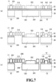
Figure 9 provides views for explanation of dimensions of throughholes 154 formed in the deformingportion 151 and the attachingportion 152 of theconduction portion 15. The same applies to the throughholes 144 formed in the deformingportion 141 and the attachingportion 142 of theconduction portion 14 and the description will not be repeated.Figure 9 (a) is a plan view illustrating a part of theconduction portion 15 and illustrates a phase prior to etching of theBOX layer 2B by BHF as illustrated inFigure 7 (a) . - The
BOX layer 2B in an exposed portion in the plan view ofFigure 9 (a) and theBOX layer 2B between the attachingportion 152 illustrated inFigure 9 (b) and the moveable electrodejoint portion 130 formed in thehandle layer 2A are removed by etching using BHF as illustrated inFigure 7 (b) . Since the etching of theBOX layer 2B by etchant entering into the throughholes 154 and aslot 155 proceeds isotropically, as illustrated inFigure 9 (c) , as the thickness of theBOX layer 2B in the exposed portion decreases, theBOX layer 2B under theframe portion 150 indicated by a symbol R1 and theBOX layer 2B under the attachingportion 152 indicated by a symbol R2 will also be etched in right and left directions in the figure. - At the completion of etching when the thickness of
BOX layer 2B in the exposed portion reaches zero as inFigure 9 (d) , theBOX layer 2B under the attachingportion 152 will be removed completely. Similarly, theBOX layer 2B under the deformingportion 151 in which the throughholes 154 are formed is also removed, leaving the deformingportion 151 in a cantilevered shape.Figure 10 is a schematic view of theconduction portion 15 after theBOX layer 2B has been removed. A pair of deformingportions 151 formed on opposite sides of the attachingportion 152 constitutes a cantilever extending from theframe portion 150, and the attachingportion 152 is connected to the distal end of the deformingportion 151 with thejoint portion 153 interposed therebetween. The attachingportion 152 extends in a folding back manner in a direction from the distal end of the deformingportion 151 to theframe portion 150. - As a result of the etching in
Figure 9 (d) , as illustrated inFigure 10 , the deformingportion 151 deforms in a direction of the moveable electrodejoint portion 130, and the distal end of the deformingportion 151 and the attachingportion 152 connected to the distal end adhere on a top face of the moveable electrodejoint portion 130 due to a stiction phenomenon. The moveable electrodejoint portion 130 formed in thehandle layer 2A and theconduction portion 15 formed in thedevice layer 2C are thereby mechanically and electrically connected into electrical continuity. As illustrated inFigure 2 , the moveable electrodejoint portion 130 is elastically supported in thehandle layer 2A of theframe body 10 with thebeam portion 131 interposed therebetween and theconduction portion 15 is connected to themoveable electrode portion 12, which means that themoveable electrode portion 12 is electrically continuous with thehandle layer 2A of theframe body 10 with theconduction portion 15 interposed therebetween. - The spacing between the through
holes 154 is determined from viewpoints as described below. It is preferable to determine a spacing t1 between throughholes 154 in such a way that when the exposedBOX layer 2B is etched away by vertical etching as illustrated inFigure 9 (d) , theBOX layer 2B present under the deformingportion 151 and the attachingportion 152 is removed substantially at the same time by lateral etching effected by etchant entering from the throughholes 154. As a matter of course, the spacing t1 may be determined in such a way that before the exposedBOX layer 2B is removed by vertical etching, adjacent throughholes 154 are brought into communication on theBOX layer 2B side. In other words, assuming that the thickness of theBOX layer 2B is defined as t2, it is only necessary to satisfy t1≤2×t2. - With regard to the
conduction portion 14 provided in the frame body 10 (seeFigure 4 ), it also has a structure similar to theconduction portion 15, and as illustrated inFigure 4 , the distal end of the deformingportion 141 in a cantilevered shape and the attachingportion 142 adhere to thehandle layer 2A of theframe body 10. As a result, thedevice layer 2C in which theelectrode pad 145 is formed and thehandle layer 2A of theframe body 10 are electrically continuous with each other. Accordingly, generated electric power can be extracted from theelectrode pad 145 of theconduction portion 14 and theelectrode pad 111 of the fixedelectrode portion 11 as illustrated inFigure 1 . - Advantageous effects of the vibration-driven
energy harvesting element 1 of the embodiment will now be described in comparison with a comparative example inFigure 11 . -
Figure 11 illustrates a comparative example for the vibration-drivenenergy harvesting element 1 of the embodiment. A vibration-drivenenergy harvesting element 300 illustrated inFigure 11 is different from the vibration-drivenenergy harvesting element 1 inFigure 1 in that 4 sets of elastically-supportingportions 13 are formed in thedevice layer 2C along with themoveable electrode portion 12. In the vibration-driven energy harvesting element inFigure 11 , the elastically-supportingportion 13 elastically supporting themoveable electrode portion 12 is joined to the fixedportion 30 formed in thedevice layer 2C. The fixedportion 30 is fixed on theframe body 10 formed in thehandle layer 2A with theBOX layer 2B interposed therebetween. Themoveable electrode portion 12 is electrically continuous with theelectrode pad 145 with the elastically-supportingportion 13 and the fixedportion 30 formed in thedevice layer 2C interposed therebetween. - As described above, in the comparative example illustrated in
Figure 11 , since the elastically-supportingportion 13 is formed in thedevice layer 2C along with themoveable electrode portion 12, an area E for arranging the elastically-supportingportion 13 is required in such a way that it is adjacent to a comb area separately from the comb area. The presence of the area E prevents size reduction of the vibration-driven energy harvesting element in terms of the shape seen in plan view. - (1) The vibration-driven
energy harvesting element 1 of the embodiment includes: the fixedelectrode portion 11 and themoveable electrode portion 12 formed in thedevice layer 2C of the substrate provided with thehandle layer 2A and thedevice layer 2C with theBOX layer 2B, which is an insulation layer, interposed therebetween; theframe body 10 formed from thehandle layer 2A and thedevice layer 2C disposed with theBOX layer 2B interposed therebetween, theframe body 10 supporting the fixedelectrode portion 11 in thedevice layer 2C; the elastically-supportingportion 13 formed in thehandle layer 2A and elastically supporting themoveable electrode portion 12 by thebeam portion 131 joined to thehandle layer 2A of theframe body 10; and theconduction portion 15 electrically connecting themoveable electrode portion 12 and the elastically-supportingportion 13. - As illustrated in
Figure 1 , in the vibration-drivenenergy harvesting element 1 of the embodiment, the elastically-supportingportion 13 is formed in thehandle layer 2A, themoveable comb teeth 120 and the fixedcomb teeth 110 are formed in thedevice layer 2C, and primary components of the vibration-drivenenergy harvesting element 1 are arranged in a stacked manner in the thickness direction of the substrate. As a result, the area of the vibration-driven energy harvesting element in plan view can be restrained substantially as much as a total area of an area in which themoveable comb teeth 120 and the fixedcomb teeth 110 are formed and the area of theframe body 10. In contrast, in the case of the configuration of the comparative example, the size may be made larger than the embodiment by the area E for arranging the elastically-supporting portion. In this way, with the vibration-drivenenergy harvesting element 1 of the embodiment, the footprint of the vibration-drivenenergy harvesting element 1 can be smaller than that of the prior art. In other words, the amount of power generation can be increased, while the area of element is restrained as large as that of the vibration-drivenenergy harvesting element 300 of the comparative example. - In the case of the comparative example in
Figure 11 , since themoveable electrode portion 12, the elastically-supportingportion 13, and the fixedportion 30 are formed in thecontinuous device layer 2C, generated electric power can easily be extracted through theelectrode pad 145 of the fixedportion 30 provided on theframe body 10 and theelectrode pad 111 of the fixedelectrode portion 11. - On the other hand, in the vibration-driven
energy harvesting element 1 of the embodiment, there is no immobile portion that is continuous with themoveable electrode portion 12 as with the fixedportion 30 inFigure 11 . As such, theconduction portion 15 electrically connecting themoveable electrode portion 12 and the elastically-supportingportion 13 is provided, so that thehandle layer 2A of theframe body 10 is brought into electrical connection with themoveable electrode portion 12 with the elastically-supportingportion 13 and theconduction portion 15 interposed therebetween. As a result, generated electric power can easily be extracted by connecting an output terminal to thehandle layer 2A of theframe body 10. In other words, such an output terminal can be provided on the back face side of the substrate. - (2) As illustrated in
Figure 3 , theconduction portion 15 may be configured such that it includes a plate-like member (the deformingportion 151 and the attaching portion 152) formed in thedevice layer 2C that is continuous with themoveable electrode portion 12 and facing the moveable electrodejoint portion 130 formed in thehandle layer 2A without theBOX layer 2B interposed therebetween. The plate-like member is provided with the deformingportion 151 in a cantilevered shape facing thehandle layer 2A without theBOX layer 2B interposed therebetween; and the attachingportion 152 connected to the distal end of the deformingportion 151 and extending from the distal end in a folding back manner in a root direction (x-axis minus direction) of the deformingportion 151, the attachingportion 152 being attached to thehandle layer 2A of the moveable electrodejoint portion 130. The deformingportion 151 and the attachingportion 152 have a plurality of throughholes 154 formed therein for etching away, by BHF, theBOX layer 2B between thedevice layer 2C in which the deformingportion 151 and the attachingportion 152 are formed and thehandle layer 2A of the moveable electrodejoint portion 130. Theconduction portion 14 is configured in a similar manner to theconduction portion 15 as illustrated inFigure 4 . - In the
conduction portion 15, since the deformingportion 151 in a cantilevered shape is brought into contact with thehandle layer 2A only in an area near the distal end, it is not possible to achieve a sufficient conductive state only through the deformingportion 151. Accordingly, in theconduction portion 15, the attachingportion 152 that has a folding back structure connected to the distal end of the deformingportion 151 in a cantilevered shape to ensure a sufficient contact area. - (3) Further, the
conduction portion 14 electrically connecting thehandle layer 2A of theframe body 10 and thedevice layer 2C is provided, and thereby theelectrode pad 145 electrically connected to themoveable electrode portion 12 can be arranged on the device layer side of theframe body 10. As a result, both theelectrode pads electrode pads - When the
conduction portion 14 is not to be provided, for example, as illustrated inFigure 12 , it may be possible to configure such that theelectrode pad 400 is formed in an element mounting portion of acase 40 in which the vibration-drivenenergy harvesting element 1 is accommodated, and thehandle layer 2A of theframe body 10 of the vibration-drivenenergy harvesting element 1 is attached to theelectrode pad 400. As a result, connecting wirings for extracting generated electric power to theelectrode pad 400 makes it possible to easily extract the generated electric power. - For the configurations of the
conduction portions Figures 3 and4 , but may be those illustrated inFigure 13 . In the configuration illustrated inFigure 13 (a) , a throughhole 52 that reaches thehandle layer 2A is formed and a metal depositedfilm 50 is deposited on an area including the throughhole 52. With the metal depositedfilm 50, thehandle layer 2A and thedevice layer 2C are electrically connected. Further, in the configuration illustrated inFigure 13 (b) , aconductive paste 51 is disposed in the area including the throughhole 52 such that thehandle layer 2A and thedevice layer 2C are electrically connected. - In the configuration of the embodiment illustrated in
Figure 1 described above, thedevice layer 2C is formed on theframe body 10 so as to surround theconduction portion 14 with the gap interposed therebetween. However, thedevice layer 2C in this area is not essential, and aframe body 10A as in a vibration-drivenenergy harvesting element 100 illustrated inFigure 14 may be applicable. Note that in the variation illustrated inFigure 14 , portions formed of thehandle layer 2A, that is, thehandle layer 2A of theframe body 10A and thebeam portion 131 of the elastically-supportingportion 13 are hatched. - The
beam portion 131 is joined to thehandle layer 2A of theframe body 10A and the fixedelectrode 11 is supported in thedevice layer 2C on theframe body 10A. Further, theconduction portion 14 is formed in thedevice layer 2C of theframe body 10A, and the deformingportion 141 of theconduction portion 14 and the attachingportion 142 electrically connect thehandle layer 2A of theframe body 10A and thedevice layer 2C in which theelectrode pad 145 is formed. In the configuration illustrated inFigure 14 , advantageous effects similar to those of the vibration-drivenenergy harvesting element 1 inFigure 1 described above can also be produced. - In the embodiment described above, description has been made as to the vibration-driven
energy harvesting element 1 provided with 4 sets of fixedelectrode portions 11 andmoveable electrode portions 12. However, the present invention is not limited to such a comb structure of the vibration-driven energy harvesting element of the embodiment. The present invention is also applicable to a comb electrode structure provided with one set of fixed electrode portion and moveable electrode portion. - Description has also been made as to an example of the vibration-driven energy harvesting element in which an electret film is formed on the fixed comb teeth and/or the moveable comb teeth. However, such an electret film is not essential, provided that a necessary amount of power generation can be output.
- In the embodiment described above, description has been made as to an example of the vibration-driven
energy harvesting element 1 including a fixedelectrode portion 11 having a plurality of fixedcomb teeth 110 and amoveable electrode portion 12 having a plurality ofmoveable comb teeth 120 that are arranged to interdigitate with the plurality of fixedcomb teeth 110 with a gap interposed therebetween, the vibration-drivenenergy harvesting element 1 being structured to elastically support themoveable electrode portion 12 so as to be displaceable in a direction in which an amount of insertion of the comb teeth changes. However, the present invention is not limited to the vibration-drivenenergy harvesting element 1 in such a configuration. For example, the present invention may also be applicable to a vibration-driven energy harvesting element in which fixedcomb teeth 110 andmoveable comb teeth 120 are arranged such that their comb teeth distal end faces face each other and themoveable comb teeth 120 are vibrated relative to the fixedcomb teeth 110 in a laterally sliding motion, as with the vibration-driven energy harvesting element described inJapanese Patent No. 6338070 - Various embodiments and variations have been described above. However, the present invention is not limited to the content thereof. Other aspects conceivable within the scope of technical ideas of the present invention, for example, application to MEMS sensors are also within the scope of the present invention.
- The disclosed contents of the following priority basic applications and patent publications are indicated for information.
-
Japanese Patent Application No. 2019-008337 (filed January, 22, 2019 -
Japanese Patent No. 5627130 -
Japanese Patent No. 6338070 - 1, 100... vibration-driven energy harvesting element, 2A...handle layer, 2B...BOX layer, 2C...device layer, 10, 10A...frame body, 11... fixed electrode portion, 12...moveable electrode portion, 13...elastically-supporting portion, 14, 15...conduction portion, 130...moveable electrode joint portion, 131...beam portion, 141, 151...deforming portion, 142, 152...attaching portion, 144, 154...through hole
Claims (6)
- A vibration-driven energy harvesting element (1), comprising:a fixed electrode portion (11) and a moveable electrode portion (12) formed in a second layer (2C) of a substrate provided with a first layer (2A) and the second layer (2C) with an insulation layer (2B) interposed therebetween;a frame body (10) formed from the first layer (2A) and the second layer (2C) disposed with the insulation layer (2B) interposed therebetween, the frame body (10) supporting the fixed electrode portion (11) in the second layer (2C); characterized in that it further comprisesan elastically-supporting portion (13) formed in the first layer (2A) and elastically supporting the moveable electrode portion (12) by a beam portion (131) joined to the first layer (2A) of the frame body (10); anda first conduction portion (15) electrically connecting the moveable electrode portion (12) and the elastically-supporting portion (13).
- The vibration-driven energy harvesting element (1) according to claim 1, whereinthe first conduction portion (15) includes a first plate-like member (151, 152) formed in the second layer (2C) that is continuous with the moveable electrode portion (12) and facing the elastically-supporting portion (13) without the insulation layer (2B) interposed therebetween,the first plate-like member (151, 152) has:a first deforming portion (151) in a cantilevered shape facing the elastically-supporting portion (13) without the insulation layer (2B) interposed therebetween; anda first attaching portion (152) connected to a distal end of the first deforming portion (151) in a cantilevered shape and extending from the distal end in a folding back manner in a root direction of the first deforming portion (151), the first attaching portion (152) being attached to the elastically-supporting portion (13), andthe first deforming portion (151) and the first attaching portion (152) have a plurality of holes (154) formed therein, the holes (154) passing through in a thickness direction of the first plate-like member (151, 152).
- The vibration-driven energy harvesting element (1) according to claim 1 or claim 2, further comprising
a second conduction portion (14) electrically connecting the first layer (2A) and the second layer (2C) of the frame body (10). - The vibration-driven energy harvesting element (1) according to claim 3, whereinthe second conduction portion (14) includes a second plate-like member (141, 142) formed in the second layer (2C) of the frame body (10) and facing the first layer (2A) of the frame body (10) without the insulation layer (2B) interposed therebetween,the second plate-like member (141, 142) has:a second deforming portion (141) in a cantilevered shape facing the first layer (2A) of the frame body (10) without the insulation layer (2B) interposed therebetween; anda second attaching portion (142) connected to a distal end of the second deforming portion (141) in a cantilevered shape and extending from the distal end in a folding back manner in a root direction of the second deforming portion (141), the second attaching portion (142) being attached to the first layer (2A) of the frame body (10), andthe second deforming portion (141) and the second attaching portion (142) have a plurality of holes (144) formed therein, the holes (144) passing through in a thickness direction of the second plate-like member (141,142).
- The vibration-driven energy harvesting element (1) according to any one of claims 1 to 4, whereinthe fixed electrode portion (11) has a plurality of fixed comb teeth (110),the moveable electrode portion (12) has a plurality of moveable comb teeth (120) arranged to interdigitate with the plurality of fixed comb teeth (110) with a gap interposed therebetween, andthe elastically-supporting portion (13) elastically supports the moveable electrode portion (12) so as to be displaceable in a direction in which an amount of insertion of the moveable comb teeth (120) relative to the fixed comb teeth (110) changes.
- A vibration-driven energy harvesting element (1), comprising:a fixed comb electrode (110) formed in a first layer (2A) of a substrate including the first layer (2A) and a second layer (2C) layered with an insulation layer (2B) interposed therebetweena moveable comb electrode (120) formed in the first layer (2A) and moveable relative to the fixed comb electrode (110); characterized in that it further comprisesan elastically-supporting portion (13) formed in the second layer (2C) and elastically supporting the moveable comb electrode (120); anda connecting portion (15) formed in the first layer (2A) and mechanically and electrically connecting the moveable comb electrode (120) to the elastically-supporting portion (13).
Applications Claiming Priority (2)
| Application Number | Priority Date | Filing Date | Title |
|---|---|---|---|
| JP2019008337 | 2019-01-22 | ||
| PCT/JP2020/001967 WO2020153362A1 (en) | 2019-01-22 | 2020-01-21 | Vibration power generation element |
Publications (5)
| Publication Number | Publication Date |
|---|---|
| EP3896838A1 EP3896838A1 (en) | 2021-10-20 |
| EP3896838A4 EP3896838A4 (en) | 2022-08-17 |
| EP3896838C0 EP3896838C0 (en) | 2023-07-26 |
| EP3896838B1 true EP3896838B1 (en) | 2023-07-26 |
| EP3896838B8 EP3896838B8 (en) | 2023-08-30 |
Family
ID=71735461
Family Applications (1)
| Application Number | Title | Priority Date | Filing Date |
|---|---|---|---|
| EP20744736.8A Active EP3896838B8 (en) | 2019-01-22 | 2020-01-21 | Vibration-driven energy harvesting element |
Country Status (4)
| Country | Link |
|---|---|
| EP (1) | EP3896838B8 (en) |
| JP (1) | JP7128493B2 (en) |
| CN (1) | CN113302834A (en) |
| WO (1) | WO2020153362A1 (en) |
Family Cites Families (15)
| Publication number | Priority date | Publication date | Assignee | Title |
|---|---|---|---|---|
| JPS5627130B2 (en) | 1974-03-29 | 1981-06-23 | ||
| JPS6178875A (en) | 1984-09-26 | 1986-04-22 | Osaka Soda Co Ltd | Vulcanizable halogen-containing polymer composition |
| JP2005045976A (en) * | 2003-07-25 | 2005-02-17 | Matsushita Electric Works Ltd | Electrostatic actuator |
| JP4427006B2 (en) * | 2005-05-31 | 2010-03-03 | セイコーエプソン株式会社 | Actuator and manufacturing method thereof |
| CN101827781B (en) * | 2007-10-31 | 2012-05-30 | 富士通株式会社 | Micro movable element and micro movable element array |
| JP5237705B2 (en) * | 2008-06-24 | 2013-07-17 | パナソニック株式会社 | Power generation device |
| WO2010107016A1 (en) * | 2009-03-16 | 2010-09-23 | パナソニック電工株式会社 | Mems device |
| JP2012024897A (en) * | 2010-07-26 | 2012-02-09 | Panasonic Electric Works Co Ltd | Mems device |
| JP5504298B2 (en) * | 2012-02-22 | 2014-05-28 | アオイ電子株式会社 | Vibration power generation element and manufacturing method thereof |
| JP6175868B2 (en) * | 2013-04-03 | 2017-08-09 | 株式会社豊田中央研究所 | MEMS equipment |
| JP5855602B2 (en) * | 2013-05-22 | 2016-02-09 | アオイ電子株式会社 | Electrostatic induction type electromechanical transducer and nanotweezers |
| JP2016059191A (en) * | 2014-09-11 | 2016-04-21 | ソニー株式会社 | Electrostatic device |
| JP6682106B2 (en) * | 2015-10-02 | 2020-04-15 | 株式会社鷺宮製作所 | Vibration generator |
| JP2019008337A (en) | 2015-10-26 | 2019-01-17 | 三郎 山内 | Object identification system, object identification method, program and computer storage medium |
| JP6507999B2 (en) * | 2015-11-04 | 2019-05-08 | 株式会社豊田中央研究所 | MEMS sensor |
-
2020
- 2020-01-21 CN CN202080009817.9A patent/CN113302834A/en active Pending
- 2020-01-21 JP JP2020568161A patent/JP7128493B2/en active Active
- 2020-01-21 WO PCT/JP2020/001967 patent/WO2020153362A1/en unknown
- 2020-01-21 EP EP20744736.8A patent/EP3896838B8/en active Active
Also Published As
| Publication number | Publication date |
|---|---|
| JP7128493B2 (en) | 2022-08-31 |
| JPWO2020153362A1 (en) | 2021-10-21 |
| EP3896838A1 (en) | 2021-10-20 |
| WO2020153362A1 (en) | 2020-07-30 |
| EP3896838A4 (en) | 2022-08-17 |
| EP3896838C0 (en) | 2023-07-26 |
| CN113302834A (en) | 2021-08-24 |
| EP3896838B8 (en) | 2023-08-30 |
Similar Documents
| Publication | Publication Date | Title |
|---|---|---|
| US6507138B1 (en) | Very compact, high-stability electrostatic actuator featuring contact-free self-limiting displacement | |
| US6133670A (en) | Compact electrostatic comb actuator | |
| CN100373162C (en) | Accelerometer | |
| US8833165B2 (en) | Miniaturized piezoelectric accelerometers | |
| Bakri-Kassem et al. | Novel High-$ Q $ MEMS Curled-Plate Variable Capacitors Fabricated in 0.35-$\mu {\hbox {m}} $ CMOS Technology | |
| JP2001007346A (en) | Manufacture of external force detection sensor | |
| JP2010135634A (en) | Method for manufacturing semiconductor device, and semiconductor device | |
| US7834525B2 (en) | Thin film piezoelectric transformer and method of manufacturing the same | |
| JP4117450B2 (en) | Manufacturing method of semiconductor device | |
| EP3896838B1 (en) | Vibration power generation element | |
| EP3896837A1 (en) | Vibrating power generation element and manufacturing method for vibrating power generation element | |
| WO2009104486A1 (en) | Microelectromechanical device and method for fabricating the same | |
| JPWO2005015595A1 (en) | Microswitching element and method for manufacturing the same | |
| JP2001004658A (en) | Dual-shaft semiconductor acceleration sensor and manufacture thereof | |
| US20140103778A1 (en) | Vibrator, manufacturing method of vibrator, electronic apparatus, and mobile unit | |
| EP3666726A1 (en) | Mems vibration element, production method for mems vibration element, and vibration power generation element | |
| JP2007322149A (en) | Method for manufacturing semiconductor device | |
| KR101573518B1 (en) | Ultrasonic transducer and fabricating method thereof | |
| JP3435647B2 (en) | Manufacturing method of vibration type semiconductor sensor | |
| JP2007274293A (en) | Condenser microphone | |
| Giridhar et al. | An X band RF MEMS switch based on silicon-on-glass architecture | |
| JP5376472B2 (en) | Resonator and manufacturing method thereof | |
| JP4569167B2 (en) | Manufacturing method of external force detection sensor | |
| WO2022130809A1 (en) | Vibration power generation element and method for manufacturing same | |
| KR100518828B1 (en) | MEMS structure for metal interconnection and fabrication method thereof |
Legal Events
| Date | Code | Title | Description |
|---|---|---|---|
| STAA | Information on the status of an ep patent application or granted ep patent |
Free format text: STATUS: THE INTERNATIONAL PUBLICATION HAS BEEN MADE |
|
| PUAI | Public reference made under article 153(3) epc to a published international application that has entered the european phase |
Free format text: ORIGINAL CODE: 0009012 |
|
| STAA | Information on the status of an ep patent application or granted ep patent |
Free format text: STATUS: REQUEST FOR EXAMINATION WAS MADE |
|
| 17P | Request for examination filed |
Effective date: 20210715 |
|
| AK | Designated contracting states |
Kind code of ref document: A1 Designated state(s): AL AT BE BG CH CY CZ DE DK EE ES FI FR GB GR HR HU IE IS IT LI LT LU LV MC MK MT NL NO PL PT RO RS SE SI SK SM TR |
|
| DAV | Request for validation of the european patent (deleted) | ||
| DAX | Request for extension of the european patent (deleted) | ||
| A4 | Supplementary search report drawn up and despatched |
Effective date: 20220715 |
|
| RIC1 | Information provided on ipc code assigned before grant |
Ipc: B81B 3/00 20060101ALI20220711BHEP Ipc: H02N 1/08 20060101AFI20220711BHEP |
|
| GRAP | Despatch of communication of intention to grant a patent |
Free format text: ORIGINAL CODE: EPIDOSNIGR1 |
|
| STAA | Information on the status of an ep patent application or granted ep patent |
Free format text: STATUS: GRANT OF PATENT IS INTENDED |
|
| INTG | Intention to grant announced |
Effective date: 20230301 |
|
| GRAS | Grant fee paid |
Free format text: ORIGINAL CODE: EPIDOSNIGR3 |
|
| GRAA | (expected) grant |
Free format text: ORIGINAL CODE: 0009210 |
|
| STAA | Information on the status of an ep patent application or granted ep patent |
Free format text: STATUS: THE PATENT HAS BEEN GRANTED |
|
| AK | Designated contracting states |
Kind code of ref document: B1 Designated state(s): AL AT BE BG CH CY CZ DE DK EE ES FI FR GB GR HR HU IE IS IT LI LT LU LV MC MK MT NL NO PL PT RO RS SE SI SK SM TR |
|
| REG | Reference to a national code |
Ref country code: CH Ref legal event code: EP |
|
| REG | Reference to a national code |
Ref country code: CH Ref legal event code: PK Free format text: BERICHTIGUNG B8 |
|
| REG | Reference to a national code |
Ref country code: IE Ref legal event code: FG4D |
|
| REG | Reference to a national code |
Ref country code: DE Ref legal event code: R096 Ref document number: 602020014526 Country of ref document: DE |
|
| U01 | Request for unitary effect filed |
Effective date: 20230726 |
|
| U07 | Unitary effect registered |
Designated state(s): AT BE BG DE DK EE FI FR IT LT LU LV MT NL PT SE SI Effective date: 20230731 |
|
| REG | Reference to a national code |
Ref country code: LT Ref legal event code: MG9D |
|
| PG25 | Lapsed in a contracting state [announced via postgrant information from national office to epo] |
Ref country code: GR Free format text: LAPSE BECAUSE OF FAILURE TO SUBMIT A TRANSLATION OF THE DESCRIPTION OR TO PAY THE FEE WITHIN THE PRESCRIBED TIME-LIMIT Effective date: 20231027 |
|
| PG25 | Lapsed in a contracting state [announced via postgrant information from national office to epo] |
Ref country code: IS Free format text: LAPSE BECAUSE OF FAILURE TO SUBMIT A TRANSLATION OF THE DESCRIPTION OR TO PAY THE FEE WITHIN THE PRESCRIBED TIME-LIMIT Effective date: 20231126 |
|
| PG25 | Lapsed in a contracting state [announced via postgrant information from national office to epo] |
Ref country code: RS Free format text: LAPSE BECAUSE OF FAILURE TO SUBMIT A TRANSLATION OF THE DESCRIPTION OR TO PAY THE FEE WITHIN THE PRESCRIBED TIME-LIMIT Effective date: 20230726 Ref country code: NO Free format text: LAPSE BECAUSE OF FAILURE TO SUBMIT A TRANSLATION OF THE DESCRIPTION OR TO PAY THE FEE WITHIN THE PRESCRIBED TIME-LIMIT Effective date: 20231026 Ref country code: IS Free format text: LAPSE BECAUSE OF FAILURE TO SUBMIT A TRANSLATION OF THE DESCRIPTION OR TO PAY THE FEE WITHIN THE PRESCRIBED TIME-LIMIT Effective date: 20231126 Ref country code: HR Free format text: LAPSE BECAUSE OF FAILURE TO SUBMIT A TRANSLATION OF THE DESCRIPTION OR TO PAY THE FEE WITHIN THE PRESCRIBED TIME-LIMIT Effective date: 20230726 Ref country code: GR Free format text: LAPSE BECAUSE OF FAILURE TO SUBMIT A TRANSLATION OF THE DESCRIPTION OR TO PAY THE FEE WITHIN THE PRESCRIBED TIME-LIMIT Effective date: 20231027 |
|
| U20 | Renewal fee paid [unitary effect] |
Year of fee payment: 5 Effective date: 20231227 |
|
| PG25 | Lapsed in a contracting state [announced via postgrant information from national office to epo] |
Ref country code: PL Free format text: LAPSE BECAUSE OF FAILURE TO SUBMIT A TRANSLATION OF THE DESCRIPTION OR TO PAY THE FEE WITHIN THE PRESCRIBED TIME-LIMIT Effective date: 20230726 |