EP3896733A1 - Semiconductor package component, base substrate for rf transistor, and manufacturing method thereof - Google Patents
Semiconductor package component, base substrate for rf transistor, and manufacturing method thereof Download PDFInfo
- Publication number
- EP3896733A1 EP3896733A1 EP19895728.4A EP19895728A EP3896733A1 EP 3896733 A1 EP3896733 A1 EP 3896733A1 EP 19895728 A EP19895728 A EP 19895728A EP 3896733 A1 EP3896733 A1 EP 3896733A1
- Authority
- EP
- European Patent Office
- Prior art keywords
- base substrate
- layer
- protrusion
- semiconductor package
- metal
- Prior art date
- Legal status (The legal status is an assumption and is not a legal conclusion. Google has not performed a legal analysis and makes no representation as to the accuracy of the status listed.)
- Pending
Links
Images


Classifications
-
- H—ELECTRICITY
- H10—SEMICONDUCTOR DEVICES; ELECTRIC SOLID-STATE DEVICES NOT OTHERWISE PROVIDED FOR
- H10W—GENERIC PACKAGES, INTERCONNECTIONS, CONNECTORS OR OTHER CONSTRUCTIONAL DETAILS OF DEVICES COVERED BY CLASS H10
- H10W40/00—Arrangements for thermal protection or thermal control
- H10W40/20—Arrangements for cooling
- H10W40/25—Arrangements for cooling characterised by their materials
- H10W40/258—Metallic materials
-
- H—ELECTRICITY
- H10—SEMICONDUCTOR DEVICES; ELECTRIC SOLID-STATE DEVICES NOT OTHERWISE PROVIDED FOR
- H10W—GENERIC PACKAGES, INTERCONNECTIONS, CONNECTORS OR OTHER CONSTRUCTIONAL DETAILS OF DEVICES COVERED BY CLASS H10
- H10W20/00—Interconnections in chips, wafers or substrates
- H10W20/40—Interconnections external to wafers or substrates, e.g. back-end-of-line [BEOL] metallisations or vias connecting to gate electrodes
- H10W20/41—Interconnections external to wafers or substrates, e.g. back-end-of-line [BEOL] metallisations or vias connecting to gate electrodes characterised by their conductive parts
- H10W20/44—Conductive materials thereof
- H10W20/4403—Conductive materials thereof based on metals, e.g. alloys, metal silicides
- H10W20/4421—Conductive materials thereof based on metals, e.g. alloys, metal silicides the principal metal being copper
-
- H—ELECTRICITY
- H10—SEMICONDUCTOR DEVICES; ELECTRIC SOLID-STATE DEVICES NOT OTHERWISE PROVIDED FOR
- H10W—GENERIC PACKAGES, INTERCONNECTIONS, CONNECTORS OR OTHER CONSTRUCTIONAL DETAILS OF DEVICES COVERED BY CLASS H10
- H10W40/00—Arrangements for thermal protection or thermal control
- H10W40/20—Arrangements for cooling
- H10W40/25—Arrangements for cooling characterised by their materials
- H10W40/255—Arrangements for cooling characterised by their materials having a laminate or multilayered structure, e.g. direct bond copper [DBC] ceramic substrates
-
- H—ELECTRICITY
- H10—SEMICONDUCTOR DEVICES; ELECTRIC SOLID-STATE DEVICES NOT OTHERWISE PROVIDED FOR
- H10W—GENERIC PACKAGES, INTERCONNECTIONS, CONNECTORS OR OTHER CONSTRUCTIONAL DETAILS OF DEVICES COVERED BY CLASS H10
- H10W44/00—Electrical arrangements for controlling or matching impedance
- H10W44/20—Electrical arrangements for controlling or matching impedance at high-frequency [HF] or radio frequency [RF]
-
- H—ELECTRICITY
- H10—SEMICONDUCTOR DEVICES; ELECTRIC SOLID-STATE DEVICES NOT OTHERWISE PROVIDED FOR
- H10W—GENERIC PACKAGES, INTERCONNECTIONS, CONNECTORS OR OTHER CONSTRUCTIONAL DETAILS OF DEVICES COVERED BY CLASS H10
- H10W70/00—Package substrates; Interposers; Redistribution layers [RDL]
- H10W70/01—Manufacture or treatment
- H10W70/04—Manufacture or treatment of leadframes
-
- H—ELECTRICITY
- H10—SEMICONDUCTOR DEVICES; ELECTRIC SOLID-STATE DEVICES NOT OTHERWISE PROVIDED FOR
- H10W—GENERIC PACKAGES, INTERCONNECTIONS, CONNECTORS OR OTHER CONSTRUCTIONAL DETAILS OF DEVICES COVERED BY CLASS H10
- H10W70/00—Package substrates; Interposers; Redistribution layers [RDL]
- H10W70/60—Insulating or insulated package substrates; Interposers; Redistribution layers
- H10W70/67—Insulating or insulated package substrates; Interposers; Redistribution layers characterised by their insulating layers or insulating parts
- H10W70/69—Insulating materials thereof
- H10W70/692—Ceramics or glasses
-
- H—ELECTRICITY
- H10—SEMICONDUCTOR DEVICES; ELECTRIC SOLID-STATE DEVICES NOT OTHERWISE PROVIDED FOR
- H10W—GENERIC PACKAGES, INTERCONNECTIONS, CONNECTORS OR OTHER CONSTRUCTIONAL DETAILS OF DEVICES COVERED BY CLASS H10
- H10W76/00—Containers; Fillings or auxiliary members therefor; Seals
- H10W76/10—Containers or parts thereof
- H10W76/12—Containers or parts thereof characterised by their shape
- H10W76/13—Containers comprising a conductive base serving as an interconnection
- H10W76/134—Containers comprising a conductive base serving as an interconnection having other interconnections parallel to the conductive base
-
- H—ELECTRICITY
- H10—SEMICONDUCTOR DEVICES; ELECTRIC SOLID-STATE DEVICES NOT OTHERWISE PROVIDED FOR
- H10W—GENERIC PACKAGES, INTERCONNECTIONS, CONNECTORS OR OTHER CONSTRUCTIONAL DETAILS OF DEVICES COVERED BY CLASS H10
- H10W90/00—Package configurations
- H10W90/811—Multiple chips on leadframes
-
- H—ELECTRICITY
- H10—SEMICONDUCTOR DEVICES; ELECTRIC SOLID-STATE DEVICES NOT OTHERWISE PROVIDED FOR
- H10W—GENERIC PACKAGES, INTERCONNECTIONS, CONNECTORS OR OTHER CONSTRUCTIONAL DETAILS OF DEVICES COVERED BY CLASS H10
- H10W44/00—Electrical arrangements for controlling or matching impedance
- H10W44/20—Electrical arrangements for controlling or matching impedance at high-frequency [HF] or radio frequency [RF]
- H10W44/203—Electrical connections
- H10W44/206—Wires
-
- H—ELECTRICITY
- H10—SEMICONDUCTOR DEVICES; ELECTRIC SOLID-STATE DEVICES NOT OTHERWISE PROVIDED FOR
- H10W—GENERIC PACKAGES, INTERCONNECTIONS, CONNECTORS OR OTHER CONSTRUCTIONAL DETAILS OF DEVICES COVERED BY CLASS H10
- H10W44/00—Electrical arrangements for controlling or matching impedance
- H10W44/20—Electrical arrangements for controlling or matching impedance at high-frequency [HF] or radio frequency [RF]
- H10W44/226—Electrical arrangements for controlling or matching impedance at high-frequency [HF] or radio frequency [RF] for HF amplifiers
-
- H—ELECTRICITY
- H10—SEMICONDUCTOR DEVICES; ELECTRIC SOLID-STATE DEVICES NOT OTHERWISE PROVIDED FOR
- H10W—GENERIC PACKAGES, INTERCONNECTIONS, CONNECTORS OR OTHER CONSTRUCTIONAL DETAILS OF DEVICES COVERED BY CLASS H10
- H10W44/00—Electrical arrangements for controlling or matching impedance
- H10W44/20—Electrical arrangements for controlling or matching impedance at high-frequency [HF] or radio frequency [RF]
- H10W44/226—Electrical arrangements for controlling or matching impedance at high-frequency [HF] or radio frequency [RF] for HF amplifiers
- H10W44/234—Arrangements for impedance matching
-
- H—ELECTRICITY
- H10—SEMICONDUCTOR DEVICES; ELECTRIC SOLID-STATE DEVICES NOT OTHERWISE PROVIDED FOR
- H10W—GENERIC PACKAGES, INTERCONNECTIONS, CONNECTORS OR OTHER CONSTRUCTIONAL DETAILS OF DEVICES COVERED BY CLASS H10
- H10W72/00—Interconnections or connectors in packages
- H10W72/851—Dispositions of multiple connectors or interconnections
- H10W72/874—On different surfaces
- H10W72/884—Die-attach connectors and bond wires
-
- H—ELECTRICITY
- H10—SEMICONDUCTOR DEVICES; ELECTRIC SOLID-STATE DEVICES NOT OTHERWISE PROVIDED FOR
- H10W—GENERIC PACKAGES, INTERCONNECTIONS, CONNECTORS OR OTHER CONSTRUCTIONAL DETAILS OF DEVICES COVERED BY CLASS H10
- H10W90/00—Package configurations
- H10W90/701—Package configurations characterised by the relative positions of pads or connectors relative to package parts
- H10W90/751—Package configurations characterised by the relative positions of pads or connectors relative to package parts of bond wires
- H10W90/756—Package configurations characterised by the relative positions of pads or connectors relative to package parts of bond wires between a chip and a stacked lead frame, conducting package substrate or heat sink
Definitions
- the present invention relates to a semiconductor package component, a base substrate for an RF transistor, and a method for manufacturing the same. More particularly, it relates to a base substrate for an RF transistor formed with a protrusion and a method for manufacturing the same. More particularly, it relates to a semiconductor package component, a base substrate for an RF transistor, and a manufacturing method thereof capable of adjusting impedance matching of an RF transistor by connecting a die chip and a lead frame with a wire so that a length of the wire is reduced as much as the protruding height of the base substrate.
- a semiconductor packaged RF power device typically includes a die chip mounted on a base and mounted within a semiconductor package.
- An RF input signal is provided to a transistor through an RF input lead extending from outside the package into the package, and an RF output signal is transmitted from the device through an RF output lead extending from inside the package to an outside.
- Related technology 1 discloses an electronic RF device and a manufacturing method thereof in which an operating bandwidth, power efficiency, etc. is controlled by correcting a parasitic capacitance of a transistor with an electrical signal passing through an input lead and an output lead.
- Related technology 2 discloses a packaged RF transistor device that includes an RF input lead and RF output lead coupled to an RF transistor cell, and a coupled output matching network.
- the upper capacitor plate of a capacitor is coupled to the output terminal of the RF transistor cell to provide impedance matching to the input of the transistor at the fundamental operating frequency of the transistor.
- Related technology 3 discloses a substrate for a high-frequency semiconductor and a manufacturing method thereof in which a thermal expansion coefficient and an insulator insulating between a lead frame and a substrate are substantially the same, and at the same time heat dissipation effect is improved with high thermal conductivity.
- the present invention is considered to solve the above problems, and an object of the present invention is to provide a semiconductor package component, a base substrate for an RF transistor, and a manufacturing method thereof capable of adjusting the impedance matching of an RF transistor by mounting a die chip on the base substrate, forming a protrusion on the base substrate, mounting the die chip on the protrusion and connecting the die chip and a lead frame with a wire so that a length of the wire is reduced as much as a protruding height.
- the present invention provides a semiconductor package component including: a base substrate; a ceramic layer formed on an upper portion of the base substrate; a lead frame formed on an upper portion of the ceramic layer; and a die chip mounted on the upper portion of the base substrate.
- a protrusion is formed on the base substrate, the die chip is mounted on the protrusion, and the die chip and the lead frame are connected with a wire.
- the present invention provides a method of manufacturing a semiconductor package component including a first step of forming a ceramic layer on an upper portion of a base substrate; a second step of forming a lead frame on an upper portion of the ceramic layer; and a third step of mounting a die chip on the upper portion of the base substrate.
- a protrusion is formed on the base substrate, the die chip is mounted on the protrusion, and the die chip and the lead frame are connected with a wire.
- a semiconductor package component and a manufacturing method thereof in which the base substrate is a metal substrate are provided.
- a semiconductor package component and a manufacturing method thereof in which the base substrate is formed in a multi-layer structure are provided.
- a semiconductor package component and a manufacturing method thereof in which the base substrate formed in a multi-layer structure includes a first copper layer, a copper-molybdenum alloy layer formed on an upper portion of the first copper layer, and a second copper layer formed on the copper-molybdenum alloy layer are provided.
- a semiconductor package component and a manufacturing method thereof in which the protrusion is in integral with the base substrate are provided.
- a semiconductor package component and a manufacturing method thereof in which a height of the ceramic layer is 0.4mm to 0.7mm are provided.
- a semiconductor package component and a manufacturing method thereof in which a height of the protrusion is 0.2 mm to 0.6 mm are provided.
- a semiconductor package component and a manufacturing method thereof in which a height of the protrusion is lower than a height of the ceramic layer are provided.
- a semiconductor package component and a manufacturing method thereof in which the ceramic layer is formed in a shape that surrounds an outer periphery of the protrusion are provided.
- a semiconductor package component and a manufacturing method thereof in which an area of the protrusion is larger than an area of the die chip are provided.
- a semiconductor package component and a manufacturing method thereof in which the protrusion is not in contact with the ceramic layer are provided.
- the present invention provides a base substrate for an RF transistor made of a metal, including a protrusion provided on one side of the base substrate.
- Another example of the present invention provides a base substrate for an RF transistor in which the base substrate is formed in a multi-layer.
- the base substrate includes a base intermediate layer; a first metal layer provided on one surface of the base intermediate layer; and a second metal layer provided on the other surface of the base intermediate layer.
- Another example of the present invention provides a base substrate for an RF transistor in which the base substrate has a thermal expansion coefficient of 4 to 9ppm / °C and a thermal conductivity of 140 to 240W /m ⁇ K.
- Another example of the present invention provides a base substrate for an RF transistor in which the base intermediate layer is a copper-molybdenum alloy layer, and the first metal layer and the second metal layer include a copper layer.
- Another example of the present invention provides a base substrate for an RF transistor in which the first metal layer and the second metal layer have a melting structure in which the metal is melted and then re-hardened.
- Another example of the present invention provides a base substrate for an RF transistor in which the protrusion is formed by welding or integrally with the base substrate.
- the present invention provides a method of manufacturing a base substrate for an RF transistor made of metal, including forming a protrusion on one side of the base substrate.
- Another example of the present invention provides a method of manufacturing a base substrate for an RF transistor in which the bae substrate is formed in a multi-layer.
- Another example of the present invention provides a method of manufacturing a base substrate for an RF transistor in which the step of forming the base substrate in the multi-layer includes the steps of: preparing a base intermediate layer; and forming a metal layer by forming a first metal layer and a second metal layer on both surfaces of the base intermediate layer, respectively.
- Another example of the present invention provides a method of manufacturing a base substrate for an RF transistor in which the base substrate has a thermal expansion coefficient of 4 to 9ppm / °C and a thermal conductivity of 140 to 240W /m ⁇ K.
- Another example of the present invention provides a method of manufacturing a base substrate for an RF transistor in which the base intermediate layer is a copper-molybdenum alloy layer, and the first metal layer and the second metal layer are a copper layer.
- Another example of the present invention provides a method of manufacturing a base substrate for an RF transistor in which the first metal layer and the second metal layer have a melting structure in which the metal is melted and then re-hardened.
- Another example of the present invention provides a method of manufacturing a base substrate for an RF transistor in which the protrusion is formed by welding or integrally with the base substrate.
- Another example of the present invention provides a method of manufacturing a base substrate for an RF transistor in which the protrusion is formed by processing with an end mill.
- Another example of the present invention provides a method of manufacturing a base substrate for an RF transistor in which the protrusion is formed by press processing.
- the length of the wire is reduced as much as the protruding height of the base substrate.
- the impedance matching of the RF transistor can be adjusted, and the RF transistor has excellent thermal conductivity, thermal expansion coefficient, and reliability.
- FIG. 1 shows a semiconductor package component of the present invention.
- the semiconductor package component 100 of the present invention includes a base substrate 10, a ceramic layer 20 formed on the upper portion of the base substrate 10, and a lead frame 30 formed on the upper portion of the ceramic layer 20.
- a protrusion 40 may be formed on the upper portion of the base substrate 10.
- FIG. 2 shows an example of a base substrate of the present invention.
- the base substrate 10 may use a metal substrate.
- the metal substrate may be manufactured by casting any one of copper (Cu), silver (Ag), aluminum (Al), nickel (Ni), tin (Sn), and molybdenum (Mo), and alloys thereof or a mixture of other metals may also be used.
- alloys such as TiCu, NiTi, TiCu, NiNb, CuMo, TiAg and the like may be used.
- a single layer structure 10A or a multi-layer structure may be used for the base substrate 10.
- a multi-layer structure two or three more layers may be used, and as shown in (b) of FIG. 2 , three-layer structures 11, 12, and 13 may be used.
- the base substrate 10 may include a base intermediate layer 12; a first metal layer 11 provided on one surface of the base intermediate layer 12; and a second metal layer 13 provided on the other surface of the base intermediate layer 12.
- the material of the base intermediate layer 12 may be any one of copper (Cu), aluminum (Al), silver (Ag), gold (Au), and molybdenum (Mo) or an alloy thereof
- the first metal layer 11 and the second metal layer 13 may be any one of copper (Cu), aluminum (Al), silver (Ag), gold (Au), molybdenum (Mo) or an alloy thereof, but the first metal layer 11 and the second metal layer 13 are preferably of the same type.
- the base intermediate layer 12 is formed of a copper-molybdenum alloy layer
- the first metal layer 11 and the second metal layer 13 are formed of a copper layer, it has the effect of reducing the thermal expansion coefficient of the base substrate 10 and improving the thermal conductivity.
- the thermal expansion coefficients of the first metal layer 11 and the second metal layer 13 are preferably smaller than that of the base intermediate layer 12, and the thermal conductivities of the first metal layer 11 and the second metal layer 13 are preferably smaller than that of the base intermediate layer 12. That is, preferably, the first metal layer 11 and the second metal layer 13 are formed of the metals whose thermal expansion coefficient and thermal conductivity are smaller than the thermal expansion coefficient and thermal conductivity of the base intermediate layer 12, and they are laminated on both surfaces of the base intermediate layer 12, respectively.
- the base substrate 10 having the multi-layer structure is a metal substrate for satisfying a specific expansion rate, and as an example, there is a metal substrate having the thermal expansion coefficient of 4 to 9 ppm/° C.
- the metal substrate having the multi-layer structure according to the present invention is the base substrate 10 that satisfies a specific thermal conductivity as well as a specific expansion rate, and as an example, there is a metal substrate having a thermal conductivity of 140 to 240 W/m ⁇ K.
- the first metal layer 11 and the second metal layer 13 are brazing bonded to the base intermediate layer 12 through a metal foil.
- the first metal layer 11 and the second metal layer 13 may be bonded to the base intermediate layer 12 using a metal foil, or may be bonded by brazing using a deposition layer.
- the first metal layer 11 and the second metal layer 13 may have a melting structure in which the metal is melted, and then re-hardened.
- the ceramic layer 20 of the present invention may be formed of any one ceramic material of Zirconia Toughened Alumina (ZTA), aluminum nitride (AlN), aluminum oxide (Al 2 O 3 ), and silicon nitride (SiN, Si 3 N 4 ).
- the ceramic layer 20 may use a synthetic ceramic material including at least one of ZTA, aluminum nitride, aluminum oxide, and silicon nitride.
- the ceramic layer 20 may have a composition ratio of about 9% to 15% of ZTA and the remainder (about 85% to 91%) of at least one of aluminum nitride, aluminum oxide, and silicon nitride.
- the ceramic layer 20 may be formed to have a thickness of about 0.4 mm to 0.7 mm depending on the composition ratio. In this case, a fine protrusion may be formed on the surface of the ceramic layer 20 through chemical or physical polishing in order to strengthen the bonding force with the base substrate 10.
- the ceramic layer 20 may be formed in a shape that surrounds the outer periphery of the protrusion 40. According to the design of the semiconductor package component, it may be formed in a polygonal shape such as a circle, an ellipse, a square, a pentagon, etc.
- the protrusion 40 of the present invention may be positioned in the center of the base substrate 10.
- the protrusion 40 may be bonded to the upper portion of the base substrate 10 by welding or the like.
- the protrusion 40 may be processed integrally with the base substrate 10.
- the second metal layer 13 and the protrusion 40 may be integrally processed.
- the process of bonding the protrusion 40 to the base substrate 10 is omitted, thereby improving process efficiency and reducing the occurrence of errors due to welding.
- the protrusion 40 may have a tetrahedral shape. Alternatively, it may have a cylindrical shape, and may be appropriately used according to the semiconductor design.
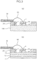
- FIG. 3 (a) is a cross-sectional view of a semiconductor package component in which a base substrate has a single layer structure, and (b) is a cross-sectional view showing a semiconductor package component in which a base substrate has a multi-layer structure.
- the area of the protrusion 40 is shown to be the same as that of the die chip 50 in (a) and (b) of FIG. 3 , but the area of the protrusion 40 may be larger than the area of the die chip 50. In terms of stably bonding the die chip 50 to the protrusion 40 and reducing an alignment error, the area of the protrusion 40 is more preferably larger than that of the die chip 50. However, when the protrusion 40 comes into contact with the ceramic layer 20, a short circuit is likely to occur, so it is preferable that the protrusion 40 does not contact the ceramic layer 20.
- the height of the protrusion 40 may be formed to have a thickness of about 0.2 mm to 0.6 mm in consideration of the height difference with the ceramic layer 20. More preferably, it may be formed to have a thickness of 0.3 mm to 0.5 mm. In this case, the height of the protrusion 40 is preferably formed to be lower than the height of the ceramic layer 20.
- the ratio of r and k may be 1:0.5 to 1:0.8.
- the ratio of r and k is more preferably 1:0.6 to 1:0.7. If the ratio of r and k is less than 0.5, the effect of impedance matching during wire bonding of the transistor is small, and if the ratio of r and k exceeds 0.8, the possibility of a wire short increases.
- the wire 60 electrically connects the die chip 50 and the lead frame 30, and may be formed of one or two or more alloys selected from platinum, gold, silver, copper, and the like.
- one wire 60 is illustrated as connecting the die chip 50 and the lead frame 30.
- an RF input signal may be provided to the transistor through the RF input lead frame extending from the outside of the semiconductor package component to the inside of the semiconductor package component, and an RF output signal may be transmitted from the device through the RF output lead frame extending from the inside of the semiconductor package component to an outside.
- the semiconductor package of the present invention may include a ceramic cover (not shown) for protecting the semiconductor package component 100.
- the semiconductor package of the present invention can be used for an RF transistor.
- the RF power transistor may be, for example, a metal-oxide semiconductor field-effect transistor (MOSFET), a lateral diffused metal-oxide semiconductor transistor (LDMOST), a bipolar junction transistor (BJT), a junction field-effect transistor (JFET), a heterojunction bipolar transistor (HBT), and the like.
- An RF power transistor can be used to generate RF power in an electronic RF device.
- a base intermediate layer preparation step (S100) may be included.
- a multilayered base substrate forming step may include the base intermediate layer preparation step; and a metal layer forming step (S200) in which a first metal layer and a second metal layer are formed on both surfaces of the base intermediate layer, respectively.
- the base substrate forming step may further include a deposition step (S110) in which a first metal foil and a second metal foil made of a metal material having a smaller thermal expansion coefficient than that of the base intermediate layer are prepared, and a first deposition layer and a second deposition layer for brazing bonding are formed on one surface of the first metal foil and one surface of the second metal foil, respectively.
- a deposition step S110 in which a first metal foil and a second metal foil made of a metal material having a smaller thermal expansion coefficient than that of the base intermediate layer are prepared, and a first deposition layer and a second deposition layer for brazing bonding are formed on one surface of the first metal foil and one surface of the second metal foil, respectively.
- the metal layer forming step (S200) may include forming a brazing filler layer on both surfaces of the base intermediate layer, respectively (S210), and laminating and brazing the first metal foil and the second metal foil on both surfaces of the base metal substrate (S220).
- the protrusion of the present invention may be formed in the center of the base substrate (S300).
- the protrusion may be manufactured by boning to the second metal layer, which is the upper portion of the base substrate, by welding or the like, or may be manufactured by being processed integrally with the second metal layer of the base substrate.
- the process of bonding the protrusion to the second metal layer of the base substrate is omitted, thereby improving process efficiency and reducing the occurrence of errors due to welding.
- the protrusion may be formed on the second metal layer of the base substrate by pouring a molten metal into a mold having a concave portion, or may be formed by removing the remaining portions except the protrusion region in the second metal layer of the flat base substrate.
- an end mill may be used to remove portions outside the protrusion region.
- a method of forming the protrusion by press processing using a method such as stamping is also advantageous in terms of processing within a short time.
- FIG. 5 Another manufacturing example of the base substrate of the present invention will be described in FIG. 5 .
- the metal layer forming step (S200) may include the steps of immersing the base intermediate layer in the molten metal (S230), and withdrawing and curing the base intermediate layer from the molten melt (S240). Next, the first metal layer and the second metal layer may be respectively formed on both surfaces of the base intermediate layer. Then, the protrusion of the present invention may be formed in the center of the base substrate (S300).
- the base substrate for an RF transistor of the present invention and a manufacturing method thereof may be used for any kind of transistors such as a metal-oxide semiconductor field-effect transistor (MOSFET), a lateral diffused metal-oxide semiconductor transistor (LDMOST), a bipolar junction transistor (BJT), a junction field-effect transistor (JFET), a heterojunction bipolar transistor (HBT) or the like, but the present invention is not limited thereto.
- MOSFET metal-oxide semiconductor field-effect transistor
- LDMOST lateral diffused metal-oxide semiconductor transistor
- BJT bipolar junction transistor
- JFET junction field-effect transistor
- HBT heterojunction bipolar transistor
Landscapes
- Cooling Or The Like Of Semiconductors Or Solid State Devices (AREA)
- Chemical & Material Sciences (AREA)
- Engineering & Computer Science (AREA)
- Ceramic Engineering (AREA)
Abstract
Description
- The present invention relates to a semiconductor package component, a base substrate for an RF transistor, and a method for manufacturing the same. More particularly, it relates to a base substrate for an RF transistor formed with a protrusion and a method for manufacturing the same. More particularly, it relates to a semiconductor package component, a base substrate for an RF transistor, and a manufacturing method thereof capable of adjusting impedance matching of an RF transistor by connecting a die chip and a lead frame with a wire so that a length of the wire is reduced as much as the protruding height of the base substrate.
- A semiconductor packaged RF power device typically includes a die chip mounted on a base and mounted within a semiconductor package. An RF input signal is provided to a transistor through an RF input lead extending from outside the package into the package, and an RF output signal is transmitted from the device through an RF output lead extending from inside the package to an outside.
- Related technology 1 discloses an electronic RF device and a manufacturing method thereof in which an operating bandwidth, power efficiency, etc. is controlled by correcting a parasitic capacitance of a transistor with an electrical signal passing through an input lead and an output lead.
- Related technology 2 discloses a packaged RF transistor device that includes an RF input lead and RF output lead coupled to an RF transistor cell, and a coupled output matching network. The upper capacitor plate of a capacitor is coupled to the output terminal of the RF transistor cell to provide impedance matching to the input of the transistor at the fundamental operating frequency of the transistor.
- Related technology 3 discloses a substrate for a high-frequency semiconductor and a manufacturing method thereof in which a thermal expansion coefficient and an insulator insulating between a lead frame and a substrate are substantially the same, and at the same time heat dissipation effect is improved with high thermal conductivity.
- However, in the conventional base substrate for an RF power transistor, a metal base is formed in a flat plate, and thus there is a limit to impedance matching during wire bonding in the transistor. Accordingly, there is a demand for development for extending an RF bandwidth.
- The matters described in the above background art are intended to help the understanding of the background of the invention, and may include matters that are not already known to those of ordinary skill in the art to which this technology belongs.
-
- (Patent Literature 1) Related technology 1:
International Patent Laid-Open Publication WO2006/097893 - (Patent Literature 2) Related technology 2: Korean Patent Laid-Open Publication
KR2015-0039759 - (Patent Literature 3) Related technology 3: Korean Patent Laid-Open Publication
KR2017-0008695 - The present invention is considered to solve the above problems, and an object of the present invention is to provide a semiconductor package component, a base substrate for an RF transistor, and a manufacturing method thereof capable of adjusting the impedance matching of an RF transistor by mounting a die chip on the base substrate, forming a protrusion on the base substrate, mounting the die chip on the protrusion and connecting the die chip and a lead frame with a wire so that a length of the wire is reduced as much as a protruding height.
- The present invention provides a semiconductor package component including: a base substrate; a ceramic layer formed on an upper portion of the base substrate; a lead frame formed on an upper portion of the ceramic layer; and a die chip mounted on the upper portion of the base substrate. A protrusion is formed on the base substrate, the die chip is mounted on the protrusion, and the die chip and the lead frame are connected with a wire.
- The present invention provides a method of manufacturing a semiconductor package component including a first step of forming a ceramic layer on an upper portion of a base substrate; a second step of forming a lead frame on an upper portion of the ceramic layer; and a third step of mounting a die chip on the upper portion of the base substrate. A protrusion is formed on the base substrate, the die chip is mounted on the protrusion, and the die chip and the lead frame are connected with a wire.
- In addition, as an example of the present invention, a semiconductor package component and a manufacturing method thereof in which the base substrate is a metal substrate are provided.
- In addition, as an example of the present invention, a semiconductor package component and a manufacturing method thereof in which the base substrate is formed in a multi-layer structure are provided.
- In addition, as an example of the present invention, a semiconductor package component and a manufacturing method thereof in which the base substrate formed in a multi-layer structure includes a first copper layer, a copper-molybdenum alloy layer formed on an upper portion of the first copper layer, and a second copper layer formed on the copper-molybdenum alloy layer are provided.
- In addition, as an example of the present invention, a semiconductor package component and a manufacturing method thereof in which the protrusion is in integral with the base substrate are provided.
- In addition, as an example of the present invention, a semiconductor package component and a manufacturing method thereof in which a height of the ceramic layer is 0.4mm to 0.7mm are provided.
- In addition, as an example of the present invention, a semiconductor package component and a manufacturing method thereof in which a height of the protrusion is 0.2 mm to 0.6 mm are provided.
- In addition, as an example of the present invention, a semiconductor package component and a manufacturing method thereof in which a height of the protrusion is lower than a height of the ceramic layer are provided.
- In addition, as an example of the present invention, a semiconductor package component and a manufacturing method thereof in which when the height of the ceramic layer is r and the height of the protrusion is k, a ratio of r and k is 1:0.5 to 1:0.8 are provided.
- In addition, as an example of the present invention, a semiconductor package component and a manufacturing method thereof in which the ceramic layer is formed in a shape that surrounds an outer periphery of the protrusion are provided.
- In addition, as an example of the present invention, a semiconductor package component and a manufacturing method thereof in which an area of the protrusion is larger than an area of the die chip are provided.
- In addition, as an example of the present invention, a semiconductor package component and a manufacturing method thereof in which the protrusion is not in contact with the ceramic layer are provided.
- Next, the present invention provides a base substrate for an RF transistor made of a metal, including a protrusion provided on one side of the base substrate.
- Another example of the present invention provides a base substrate for an RF transistor in which the base substrate is formed in a multi-layer.
- Another example of the present invention provides a base substrate for an RF transistor in which the base substrate includes a base intermediate layer; a first metal layer provided on one surface of the base intermediate layer; and a second metal layer provided on the other surface of the base intermediate layer.
- Another example of the present invention provides a base substrate for an RF transistor in which the base substrate has a thermal expansion coefficient of 4 to 9ppm / °C and a thermal conductivity of 140 to 240W /m·K.
- Another example of the present invention provides a base substrate for an RF transistor in which the base intermediate layer is a copper-molybdenum alloy layer, and the first metal layer and the second metal layer include a copper layer.
- Another example of the present invention provides a base substrate for an RF transistor in which the first metal layer and the second metal layer have a melting structure in which the metal is melted and then re-hardened.
- Another example of the present invention provides a base substrate for an RF transistor in which the protrusion is formed by welding or integrally with the base substrate.
- The present invention provides a method of manufacturing a base substrate for an RF transistor made of metal, including forming a protrusion on one side of the base substrate.
- Another example of the present invention provides a method of manufacturing a base substrate for an RF transistor in which the bae substrate is formed in a multi-layer.
- Another example of the present invention provides a method of manufacturing a base substrate for an RF transistor in which the step of forming the base substrate in the multi-layer includes the steps of: preparing a base intermediate layer; and forming a metal layer by forming a first metal layer and a second metal layer on both surfaces of the base intermediate layer, respectively.
- Another example of the present invention provides a method of manufacturing a base substrate for an RF transistor in which the base substrate has a thermal expansion coefficient of 4 to 9ppm / °C and a thermal conductivity of 140 to 240W /m·K.
- Another example of the present invention provides a method of manufacturing a base substrate for an RF transistor in which the base intermediate layer is a copper-molybdenum alloy layer, and the first metal layer and the second metal layer are a copper layer.
- Another example of the present invention provides a method of manufacturing a base substrate for an RF transistor in which the first metal layer and the second metal layer have a melting structure in which the metal is melted and then re-hardened.
- Another example of the present invention provides a method of manufacturing a base substrate for an RF transistor in which the protrusion is formed by welding or integrally with the base substrate.
- Another example of the present invention provides a method of manufacturing a base substrate for an RF transistor in which the protrusion is formed by processing with an end mill.
- Another example of the present invention provides a method of manufacturing a base substrate for an RF transistor in which the protrusion is formed by press processing.
- According to the present invention, when connecting a die chip and a lead frame with a wire in a semiconductor package component, the length of the wire is reduced as much as the protruding height of the base substrate. Thus, the impedance matching of the RF transistor can be adjusted, and the RF transistor has excellent thermal conductivity, thermal expansion coefficient, and reliability.
-
-
FIG. 1 shows a semiconductor package component of the present invention. -
FIG. 2 shows a base substrate of the present invention. -
FIG. 3 shows a cross-sectional view of a semiconductor package component. -
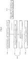
FIG. 4 shows a manufacturing example of a base substrate of the present invention. -
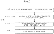
FIG. 5 shows another manufacturing example of a base substrate of the present invention. - In order to fully understand the present invention, the operational advantages of the present invention, and the objects achieved by the embodiment of the present invention, reference should be made to the accompanying drawings illustrating preferred embodiments of the present invention and the contents described in the accompanying drawings.
- In describing preferred embodiments of the present invention, well-known techniques or repetitive descriptions that may unnecessarily obscure the gist of the present invention will be reduced or omitted.
-
FIG. 1 shows a semiconductor package component of the present invention. As shown inFIG. 1 , thesemiconductor package component 100 of the present invention includes abase substrate 10, aceramic layer 20 formed on the upper portion of thebase substrate 10, and alead frame 30 formed on the upper portion of theceramic layer 20. In addition, in thesemiconductor package component 100 of the present invention, aprotrusion 40 may be formed on the upper portion of thebase substrate 10. -
FIG. 2 shows an example of a base substrate of the present invention. Thebase substrate 10 may use a metal substrate. The metal substrate may be manufactured by casting any one of copper (Cu), silver (Ag), aluminum (Al), nickel (Ni), tin (Sn), and molybdenum (Mo), and alloys thereof or a mixture of other metals may also be used. For example, alloys such as TiCu, NiTi, TiCu, NiNb, CuMo, TiAg and the like may be used. - As shown in (a) of
FIG. 2 , asingle layer structure 10A or a multi-layer structure may be used for thebase substrate 10. In the case of a multi-layer structure, two or three more layers may be used, and as shown in (b) ofFIG. 2 , three-layer structures - The
base substrate 10 may include a baseintermediate layer 12; afirst metal layer 11 provided on one surface of the baseintermediate layer 12; and asecond metal layer 13 provided on the other surface of the baseintermediate layer 12. - The material of the base
intermediate layer 12 may be any one of copper (Cu), aluminum (Al), silver (Ag), gold (Au), and molybdenum (Mo) or an alloy thereof, and thefirst metal layer 11 and thesecond metal layer 13 may be any one of copper (Cu), aluminum (Al), silver (Ag), gold (Au), molybdenum (Mo) or an alloy thereof, but thefirst metal layer 11 and thesecond metal layer 13 are preferably of the same type. In particular, when the baseintermediate layer 12 is formed of a copper-molybdenum alloy layer, and thefirst metal layer 11 and thesecond metal layer 13 are formed of a copper layer, it has the effect of reducing the thermal expansion coefficient of thebase substrate 10 and improving the thermal conductivity. - In addition, the thermal expansion coefficients of the
first metal layer 11 and thesecond metal layer 13 are preferably smaller than that of the baseintermediate layer 12, and the thermal conductivities of thefirst metal layer 11 and thesecond metal layer 13 are preferably smaller than that of the baseintermediate layer 12. That is, preferably, thefirst metal layer 11 and thesecond metal layer 13 are formed of the metals whose thermal expansion coefficient and thermal conductivity are smaller than the thermal expansion coefficient and thermal conductivity of the baseintermediate layer 12, and they are laminated on both surfaces of the baseintermediate layer 12, respectively. - The
base substrate 10 having the multi-layer structure is a metal substrate for satisfying a specific expansion rate, and as an example, there is a metal substrate having the thermal expansion coefficient of 4 to 9 ppm/° C. In addition, the metal substrate having the multi-layer structure according to the present invention is thebase substrate 10 that satisfies a specific thermal conductivity as well as a specific expansion rate, and as an example, there is a metal substrate having a thermal conductivity of 140 to 240 W/m·K. - As an example, the
first metal layer 11 and thesecond metal layer 13 are brazing bonded to the baseintermediate layer 12 through a metal foil. For example, thefirst metal layer 11 and thesecond metal layer 13 may be bonded to the baseintermediate layer 12 using a metal foil, or may be bonded by brazing using a deposition layer. Thefirst metal layer 11 and thesecond metal layer 13 may have a melting structure in which the metal is melted, and then re-hardened. - The
ceramic layer 20 of the present invention may be formed of any one ceramic material of Zirconia Toughened Alumina (ZTA), aluminum nitride (AlN), aluminum oxide (Al2O3), and silicon nitride (SiN, Si3N4). Theceramic layer 20 may use a synthetic ceramic material including at least one of ZTA, aluminum nitride, aluminum oxide, and silicon nitride. For example, theceramic layer 20 may have a composition ratio of about 9% to 15% of ZTA and the remainder (about 85% to 91%) of at least one of aluminum nitride, aluminum oxide, and silicon nitride. Theceramic layer 20 may be formed to have a thickness of about 0.4 mm to 0.7 mm depending on the composition ratio. In this case, a fine protrusion may be formed on the surface of theceramic layer 20 through chemical or physical polishing in order to strengthen the bonding force with thebase substrate 10. - The
ceramic layer 20 may be formed in a shape that surrounds the outer periphery of theprotrusion 40. According to the design of the semiconductor package component, it may be formed in a polygonal shape such as a circle, an ellipse, a square, a pentagon, etc. - The
protrusion 40 of the present invention may be positioned in the center of thebase substrate 10. Theprotrusion 40 may be bonded to the upper portion of thebase substrate 10 by welding or the like. - Alternatively, the
protrusion 40 may be processed integrally with thebase substrate 10. For example, thesecond metal layer 13 and theprotrusion 40 may be integrally processed. When theprotrusion 40 and thebase substrate 10 are integrally formed, the process of bonding theprotrusion 40 to thebase substrate 10 is omitted, thereby improving process efficiency and reducing the occurrence of errors due to welding. - As shown in (a) and (b) of
FIG. 2 , theprotrusion 40 may have a tetrahedral shape. Alternatively, it may have a cylindrical shape, and may be appropriately used according to the semiconductor design. - In
FIG. 3 , (a) is a cross-sectional view of a semiconductor package component in which a base substrate has a single layer structure, and (b) is a cross-sectional view showing a semiconductor package component in which a base substrate has a multi-layer structure. - The area of the
protrusion 40 is shown to be the same as that of thedie chip 50 in (a) and (b) ofFIG. 3 , but the area of theprotrusion 40 may be larger than the area of thedie chip 50. In terms of stably bonding thedie chip 50 to theprotrusion 40 and reducing an alignment error, the area of theprotrusion 40 is more preferably larger than that of thedie chip 50. However, when theprotrusion 40 comes into contact with theceramic layer 20, a short circuit is likely to occur, so it is preferable that theprotrusion 40 does not contact theceramic layer 20. - The height of the
protrusion 40 may be formed to have a thickness of about 0.2 mm to 0.6 mm in consideration of the height difference with theceramic layer 20. More preferably, it may be formed to have a thickness of 0.3 mm to 0.5 mm. In this case, the height of theprotrusion 40 is preferably formed to be lower than the height of theceramic layer 20. For example, when the height of theceramic layer 20 is r and the height of theprotrusion 40 is k, the ratio of r and k may be 1:0.5 to 1:0.8. The ratio of r and k is more preferably 1:0.6 to 1:0.7. If the ratio of r and k is less than 0.5, the effect of impedance matching during wire bonding of the transistor is small, and if the ratio of r and k exceeds 0.8, the possibility of a wire short increases. - The
wire 60 electrically connects thedie chip 50 and thelead frame 30, and may be formed of one or two or more alloys selected from platinum, gold, silver, copper, and the like. - In (a) and (b) of
FIG. 3 , onewire 60 is illustrated as connecting thedie chip 50 and thelead frame 30. However, an RF input signal may be provided to the transistor through the RF input lead frame extending from the outside of the semiconductor package component to the inside of the semiconductor package component, and an RF output signal may be transmitted from the device through the RF output lead frame extending from the inside of the semiconductor package component to an outside. - The semiconductor package of the present invention may include a ceramic cover (not shown) for protecting the
semiconductor package component 100. In addition, the semiconductor package of the present invention can be used for an RF transistor. The RF power transistor may be, for example, a metal-oxide semiconductor field-effect transistor (MOSFET), a lateral diffused metal-oxide semiconductor transistor (LDMOST), a bipolar junction transistor (BJT), a junction field-effect transistor (JFET), a heterojunction bipolar transistor (HBT), and the like. An RF power transistor can be used to generate RF power in an electronic RF device. - Next, with reference to
FIG. 4 , a manufacturing example of the base substrate of the present invention will be described. - A base intermediate layer preparation step (S100) may be included. In addition, a multilayered base substrate forming step may include the base intermediate layer preparation step; and a metal layer forming step (S200) in which a first metal layer and a second metal layer are formed on both surfaces of the base intermediate layer, respectively.
- As an example, the base substrate forming step may further include a deposition step (S110) in which a first metal foil and a second metal foil made of a metal material having a smaller thermal expansion coefficient than that of the base intermediate layer are prepared, and a first deposition layer and a second deposition layer for brazing bonding are formed on one surface of the first metal foil and one surface of the second metal foil, respectively.
- In addition, the metal layer forming step (S200) may include forming a brazing filler layer on both surfaces of the base intermediate layer, respectively (S210), and laminating and brazing the first metal foil and the second metal foil on both surfaces of the base metal substrate (S220).
- Then, the protrusion of the present invention may be formed in the center of the base substrate (S300). The protrusion may be manufactured by boning to the second metal layer, which is the upper portion of the base substrate, by welding or the like, or may be manufactured by being processed integrally with the second metal layer of the base substrate. When the protrusion and the second metal layer of the base substrate are integrally manufactured, the process of bonding the protrusion to the second metal layer of the base substrate is omitted, thereby improving process efficiency and reducing the occurrence of errors due to welding.
- In order to integrally manufacture the protrusion and the second metal layer of the base substrate, the protrusion may be formed on the second metal layer of the base substrate by pouring a molten metal into a mold having a concave portion, or may be formed by removing the remaining portions except the protrusion region in the second metal layer of the flat base substrate. For example, an end mill may be used to remove portions outside the protrusion region. Alternatively, a method of forming the protrusion by press processing using a method such as stamping is also advantageous in terms of processing within a short time.
- Another manufacturing example of the base substrate of the present invention will be described in
FIG. 5 . - After the base intermediate layer preparation step (S100), the metal layer forming step (S200) may include the steps of immersing the base intermediate layer in the molten metal (S230), and withdrawing and curing the base intermediate layer from the molten melt (S240). Next, the first metal layer and the second metal layer may be respectively formed on both surfaces of the base intermediate layer. Then, the protrusion of the present invention may be formed in the center of the base substrate (S300).
- The base substrate for an RF transistor of the present invention and a manufacturing method thereof may be used for any kind of transistors such as a metal-oxide semiconductor field-effect transistor (MOSFET), a lateral diffused metal-oxide semiconductor transistor (LDMOST), a bipolar junction transistor (BJT), a junction field-effect transistor (JFET), a heterojunction bipolar transistor (HBT) or the like, but the present invention is not limited thereto.
-
- 10
- base substrate
- 11
- first metal layer
- 12
- base intermediate layer
- 13
- second metal layer
- 20
- ceramic layer
- 30
- lead frame
- 40
- protrusion
- 50
- die chip
- 60
- wire
Claims (20)
- A semiconductor package component comprising:a base substrate;a ceramic layer formed on an upper portion of the base substrate;a lead frame formed on an upper portion of the ceramic layer;a die chip mounted on the upper portion of the base substrate,wherein a protrusion is formed on the base substrate, the die chip is mounted on the protrusion, and the die chip and the lead frame are connected with a wire.
- The semiconductor package component according to claim 1, wherein the base substrate is formed in a multi-layer structure, and the base substrate formed in the multi-layer structure includes a first copper layer, a copper-molybdenum alloy layer formed on an upper portion of the first copper layer, and a second copper layer formed on the copper-molybdenum alloy layer.
- The semiconductor package component according to claim 1, wherein the protrusion is in integral with the base substrate.
- The semiconductor package component according to claim 1, wherein a height of the ceramic layer is 0.4mm to 0.7mm, and a height of the protrusion is 0.2 mm to 0.6 mm.
- The semiconductor package component according to claim 1, wherein a height of the protrusion is lower than a height of the ceramic layer.
- The semiconductor package component according to claim 5, wherein, when the height of the ceramic layer is r and the height of the protrusion is k, a ratio of r and k is 1:0.5 to 1:0.8.
- The semiconductor package component according to claim 1, wherein the ceramic layer is formed in a shape that surrounds an outer periphery of the protrusion.
- The semiconductor package component according to claim 1, wherein an area of the protrusion is larger than an area of the die chip.
- The semiconductor package component according to claim 1, wherein the protrusion is not in contact with the ceramic layer.
- A base substrate for an RF transistor made of a metal, comprising:a protrusion provided on one side of the base substrate,wherein the base substrate is formed in a multi-layer.
- The base substrate for an RF transistor according to claim 10, wherein the base substrate includes:a base intermediate layer;a first metal layer provided on one surface of the base intermediate layer; anda second metal layer provided on the other surface of the base intermediate layer.
- The base substrate for an RF transistor according to claim 10, wherein the base substrate has a thermal expansion coefficient of 4 to 9ppm / °C and a thermal conductivity of 140 to 240W /m·K.
- The base substrate for an RF transistor according to claim 11, wherein the base intermediate layer is a copper-molybdenum alloy layer, and the first metal layer and the second metal layer include a copper layer.
- The base substrate for an RF transistor according to claim 11, wherein the first metal layer and the second metal layer have a melting structure in which the metal is melted and then re-hardened.
- A method of manufacturing a base substrate for an RF transistor made of metal, the method comprising the step of:
forming a protrusion on one side of the base substrate. - The method of manufacturing a base substrate for an RF transistor according to claim 15, wherein the bae substrate is formed in a multi-layer,
the step of forming the base substrate in the multi-layer including the steps of:preparing a base intermediate layer; andforming a metal layer by forming a first metal layer and a second metal layer on both surfaces of the base intermediate layer, respectively. - The method of manufacturing a base substrate for an RF transistor according to claim 15, wherein the base substrate has a thermal expansion coefficient of 4 to 9ppm / °C and a thermal conductivity of 140 to 240W /m·K.
- The method of manufacturing a base substrate for an RF transistor according to claim 16, wherein the base intermediate layer is a copper-molybdenum alloy layer, and the first metal layer and the second metal layer are a copper layer.
- The method of manufacturing a base substrate for an RF transistor according to claim 16, wherein the first metal layer and the second metal layer have a melting structure in which the metal is melted and then re-hardened.
- The method of manufacturing a base substrate for an RF transistor according to claim 15, wherein the protrusion is formed by welding or integrally with the base substrate.
Applications Claiming Priority (3)
| Application Number | Priority Date | Filing Date | Title |
|---|---|---|---|
| KR1020180159112A KR20200071401A (en) | 2018-12-11 | 2018-12-11 | Base Substrate for RF Transistor, Semiconductor Package Including The Same, Semiconductor Package Parts, and Making Method Therefor |
| KR1020180159062A KR20200071381A (en) | 2018-12-11 | 2018-12-11 | Base Substrate for RF Transistor, and Making Method Therefor |
| PCT/KR2019/016726 WO2020122482A1 (en) | 2018-12-11 | 2019-11-29 | Semiconductor package component, base substrate for rf transistor, and manufacturing method thereof |
Publications (2)
| Publication Number | Publication Date |
|---|---|
| EP3896733A1 true EP3896733A1 (en) | 2021-10-20 |
| EP3896733A4 EP3896733A4 (en) | 2022-01-26 |
Family
ID=71075670
Family Applications (1)
| Application Number | Title | Priority Date | Filing Date |
|---|---|---|---|
| EP19895728.4A Pending EP3896733A4 (en) | 2018-12-11 | 2019-11-29 | SEMICONDUCTOR PACKAGE COMPONENT, RF TRANSISTOR BASE SUBSTRATE AND METHOD OF MAKING IT |
Country Status (4)
| Country | Link |
|---|---|
| US (1) | US11869857B2 (en) |
| EP (1) | EP3896733A4 (en) |
| CN (1) | CN113196475A (en) |
| WO (1) | WO2020122482A1 (en) |
Family Cites Families (17)
| Publication number | Priority date | Publication date | Assignee | Title |
|---|---|---|---|---|
| JP2970723B2 (en) * | 1992-02-13 | 1999-11-02 | 三菱電機株式会社 | Semiconductor package and manufacturing method thereof |
| US6056186A (en) * | 1996-06-25 | 2000-05-02 | Brush Wellman Inc. | Method for bonding a ceramic to a metal with a copper-containing shim |
| US20010038140A1 (en) | 2000-04-06 | 2001-11-08 | Karker Jeffrey A. | High rigidity, multi-layered semiconductor package and method of making the same |
| EP1864328A2 (en) | 2005-03-18 | 2007-12-12 | Nxp B.V. | Method and system for output matching of rf transistors |
| JP2006351826A (en) | 2005-06-16 | 2006-12-28 | Shinko Electric Ind Co Ltd | High frequency package and semiconductor device |
| WO2008013279A1 (en) | 2006-07-28 | 2008-01-31 | Kyocera Corporation | Electronic component storing package and electronic device |
| JP2009158537A (en) * | 2007-12-25 | 2009-07-16 | Sumitomo Metal Electronics Devices Inc | Package for storing semiconductor elements |
| JP5806464B2 (en) | 2010-02-03 | 2015-11-10 | 株式会社東芝 | Semiconductor element storage package and semiconductor device using the same |
| KR20120031681A (en) | 2010-09-27 | 2012-04-04 | 삼성테크윈 주식회사 | Semiconductor package and manufacturing method thereof |
| KR20130113795A (en) * | 2012-04-06 | 2013-10-16 | 에스티에스반도체통신 주식회사 | Method for semiconductor package using a silicon substrate |
| JP2013239658A (en) * | 2012-05-17 | 2013-11-28 | Sumitomo Electric Ind Ltd | Semiconductor device |
| EP2867991B1 (en) | 2012-06-29 | 2020-03-18 | Cree, Inc. | Rf transistor packages with high frequency stabilization features |
| KR101363392B1 (en) * | 2012-10-17 | 2014-02-17 | (주)엘이디팩 | Gan semiconductor package for high power amplifier and method the same |
| KR20150049967A (en) | 2013-10-31 | 2015-05-08 | 삼성전기주식회사 | Power module package |
| KR102004785B1 (en) | 2014-03-18 | 2019-07-29 | 삼성전기주식회사 | Power Semi-Conductor package and Method of Manufacturing for the same |
| KR20170008695A (en) | 2015-07-14 | 2017-01-24 | 주식회사 아모센스 | Board for RF Semiconductor and Manufacturing Method of the Board for RF Semiconductor, RF Semiconductor thereof |
| KR102384794B1 (en) * | 2015-09-15 | 2022-04-18 | 주식회사 아모센스 | Amplification Semiconductor Package For communication |
-
2019
- 2019-11-29 EP EP19895728.4A patent/EP3896733A4/en active Pending
- 2019-11-29 CN CN201980082391.7A patent/CN113196475A/en active Pending
- 2019-11-29 US US17/413,403 patent/US11869857B2/en active Active
- 2019-11-29 WO PCT/KR2019/016726 patent/WO2020122482A1/en not_active Ceased
Also Published As
| Publication number | Publication date |
|---|---|
| EP3896733A4 (en) | 2022-01-26 |
| WO2020122482A1 (en) | 2020-06-18 |
| CN113196475A (en) | 2021-07-30 |
| US20220045023A1 (en) | 2022-02-10 |
| US11869857B2 (en) | 2024-01-09 |
Similar Documents
| Publication | Publication Date | Title |
|---|---|---|
| TWI836222B (en) | Methods for pillar connection on frontside and passive device integration on backside of die | |
| JP5450313B2 (en) | High frequency semiconductor package and manufacturing method thereof | |
| EP1909321B1 (en) | Metal-ceramic composite substrate and method for manufacturing same | |
| JP5323167B2 (en) | package | |
| US9054063B2 (en) | High power single-die semiconductor package | |
| EP2159837B1 (en) | Electronic component storing package and electronic device | |
| EP3690937B1 (en) | Cascode semiconductor device and method of manufacture | |
| US8084861B2 (en) | Connection structure semiconductor chip and electronic component including the connection structure and methods for producing the connection structure | |
| US11538795B2 (en) | Cascode semiconductor device and method of manufacture | |
| JP2012178525A (en) | Package | |
| US11869857B2 (en) | Semiconductor package component | |
| JP2012182386A (en) | Package | |
| US12500169B2 (en) | Embedded packaging structure | |
| US11862582B2 (en) | Package with elevated lead and structure extending vertically from encapsulant bottom | |
| NL2021598B1 (en) | Seed layer for electroplating eutectic AuSn solder | |
| EP2140481B1 (en) | Method and structure for reducing cracks in a dielectric layer in contact with metal | |
| KR20220136328A (en) | Making method of base substrate for rf transistor | |
| KR20200071401A (en) | Base Substrate for RF Transistor, Semiconductor Package Including The Same, Semiconductor Package Parts, and Making Method Therefor | |
| JP2009158537A (en) | Package for storing semiconductor elements | |
| US12417966B2 (en) | IPD components having SiC substrates and devices and processes implementing the same | |
| US20250015123A1 (en) | Electronic component, semiconductor device, and method of manufacturing semiconductor device | |
| JP2003197825A (en) | Semiconductor device and manufacturing method thereof | |
| EP4057340A1 (en) | Semiconductor device with a layer stack comprising a nisi layer and a niv layer for mounting on an electrically conductive layer, method for producing the same and corresponding mounted semiconductor arrangement | |
| JP2005086057A (en) | Semiconductor device and manufacturing method thereof | |
| JP2004095735A (en) | Semiconductor device |
Legal Events
| Date | Code | Title | Description |
|---|---|---|---|
| STAA | Information on the status of an ep patent application or granted ep patent |
Free format text: STATUS: THE INTERNATIONAL PUBLICATION HAS BEEN MADE |
|
| PUAI | Public reference made under article 153(3) epc to a published international application that has entered the european phase |
Free format text: ORIGINAL CODE: 0009012 |
|
| STAA | Information on the status of an ep patent application or granted ep patent |
Free format text: STATUS: REQUEST FOR EXAMINATION WAS MADE |
|
| 17P | Request for examination filed |
Effective date: 20210708 |
|
| AK | Designated contracting states |
Kind code of ref document: A1 Designated state(s): AL AT BE BG CH CY CZ DE DK EE ES FI FR GB GR HR HU IE IS IT LI LT LU LV MC MK MT NL NO PL PT RO RS SE SI SK SM TR |
|
| A4 | Supplementary search report drawn up and despatched |
Effective date: 20220107 |
|
| RIC1 | Information provided on ipc code assigned before grant |
Ipc: H03F 3/189 20060101ALN20211223BHEP Ipc: H01L 23/047 20060101ALI20211223BHEP Ipc: H01L 29/66 20060101ALI20211223BHEP Ipc: H01L 23/00 20060101ALI20211223BHEP Ipc: H01L 23/498 20060101ALI20211223BHEP Ipc: H01L 23/373 20060101ALI20211223BHEP Ipc: H01L 23/14 20060101ALI20211223BHEP Ipc: H01L 23/13 20060101ALI20211223BHEP Ipc: H01L 23/66 20060101AFI20211223BHEP |
|
| DAV | Request for validation of the european patent (deleted) | ||
| DAX | Request for extension of the european patent (deleted) |