EP3893278A1 - Array substrate and manufacturing method therefor, and display device - Google Patents
Array substrate and manufacturing method therefor, and display device Download PDFInfo
- Publication number
- EP3893278A1 EP3893278A1 EP19858705.7A EP19858705A EP3893278A1 EP 3893278 A1 EP3893278 A1 EP 3893278A1 EP 19858705 A EP19858705 A EP 19858705A EP 3893278 A1 EP3893278 A1 EP 3893278A1
- Authority
- EP
- European Patent Office
- Prior art keywords
- line
- layer
- fanout
- array substrate
- gate
- Prior art date
- Legal status (The legal status is an assumption and is not a legal conclusion. Google has not performed a legal analysis and makes no representation as to the accuracy of the status listed.)
- Granted
Links
Images


Classifications
-
- H—ELECTRICITY
- H10—SEMICONDUCTOR DEVICES; ELECTRIC SOLID-STATE DEVICES NOT OTHERWISE PROVIDED FOR
- H10D—INORGANIC ELECTRIC SEMICONDUCTOR DEVICES
- H10D86/00—Integrated devices formed in or on insulating or conducting substrates, e.g. formed in silicon-on-insulator [SOI] substrates or on stainless steel or glass substrates
- H10D86/40—Integrated devices formed in or on insulating or conducting substrates, e.g. formed in silicon-on-insulator [SOI] substrates or on stainless steel or glass substrates characterised by multiple TFTs
- H10D86/441—Interconnections, e.g. scanning lines
-
- H—ELECTRICITY
- H10—SEMICONDUCTOR DEVICES; ELECTRIC SOLID-STATE DEVICES NOT OTHERWISE PROVIDED FOR
- H10D—INORGANIC ELECTRIC SEMICONDUCTOR DEVICES
- H10D86/00—Integrated devices formed in or on insulating or conducting substrates, e.g. formed in silicon-on-insulator [SOI] substrates or on stainless steel or glass substrates
- H10D86/01—Manufacture or treatment
- H10D86/021—Manufacture or treatment of multiple TFTs
-
- H—ELECTRICITY
- H10—SEMICONDUCTOR DEVICES; ELECTRIC SOLID-STATE DEVICES NOT OTHERWISE PROVIDED FOR
- H10D—INORGANIC ELECTRIC SEMICONDUCTOR DEVICES
- H10D86/00—Integrated devices formed in or on insulating or conducting substrates, e.g. formed in silicon-on-insulator [SOI] substrates or on stainless steel or glass substrates
- H10D86/01—Manufacture or treatment
- H10D86/021—Manufacture or treatment of multiple TFTs
- H10D86/0212—Manufacture or treatment of multiple TFTs comprising manufacture, treatment or coating of substrates
-
- H—ELECTRICITY
- H10—SEMICONDUCTOR DEVICES; ELECTRIC SOLID-STATE DEVICES NOT OTHERWISE PROVIDED FOR
- H10D—INORGANIC ELECTRIC SEMICONDUCTOR DEVICES
- H10D86/00—Integrated devices formed in or on insulating or conducting substrates, e.g. formed in silicon-on-insulator [SOI] substrates or on stainless steel or glass substrates
- H10D86/40—Integrated devices formed in or on insulating or conducting substrates, e.g. formed in silicon-on-insulator [SOI] substrates or on stainless steel or glass substrates characterised by multiple TFTs
- H10D86/411—Integrated devices formed in or on insulating or conducting substrates, e.g. formed in silicon-on-insulator [SOI] substrates or on stainless steel or glass substrates characterised by multiple TFTs characterised by materials, geometry or structure of the substrates
-
- H—ELECTRICITY
- H10—SEMICONDUCTOR DEVICES; ELECTRIC SOLID-STATE DEVICES NOT OTHERWISE PROVIDED FOR
- H10D—INORGANIC ELECTRIC SEMICONDUCTOR DEVICES
- H10D86/00—Integrated devices formed in or on insulating or conducting substrates, e.g. formed in silicon-on-insulator [SOI] substrates or on stainless steel or glass substrates
- H10D86/40—Integrated devices formed in or on insulating or conducting substrates, e.g. formed in silicon-on-insulator [SOI] substrates or on stainless steel or glass substrates characterised by multiple TFTs
- H10D86/451—Integrated devices formed in or on insulating or conducting substrates, e.g. formed in silicon-on-insulator [SOI] substrates or on stainless steel or glass substrates characterised by multiple TFTs characterised by the compositions or shapes of the interlayer dielectrics
-
- H—ELECTRICITY
- H10—SEMICONDUCTOR DEVICES; ELECTRIC SOLID-STATE DEVICES NOT OTHERWISE PROVIDED FOR
- H10D—INORGANIC ELECTRIC SEMICONDUCTOR DEVICES
- H10D86/00—Integrated devices formed in or on insulating or conducting substrates, e.g. formed in silicon-on-insulator [SOI] substrates or on stainless steel or glass substrates
- H10D86/40—Integrated devices formed in or on insulating or conducting substrates, e.g. formed in silicon-on-insulator [SOI] substrates or on stainless steel or glass substrates characterised by multiple TFTs
- H10D86/60—Integrated devices formed in or on insulating or conducting substrates, e.g. formed in silicon-on-insulator [SOI] substrates or on stainless steel or glass substrates characterised by multiple TFTs wherein the TFTs are in active matrices
-
- H—ELECTRICITY
- H10—SEMICONDUCTOR DEVICES; ELECTRIC SOLID-STATE DEVICES NOT OTHERWISE PROVIDED FOR
- H10K—ORGANIC ELECTRIC SOLID-STATE DEVICES
- H10K59/00—Integrated devices, or assemblies of multiple devices, comprising at least one organic light-emitting element covered by group H10K50/00
-
- H—ELECTRICITY
- H10—SEMICONDUCTOR DEVICES; ELECTRIC SOLID-STATE DEVICES NOT OTHERWISE PROVIDED FOR
- H10K—ORGANIC ELECTRIC SOLID-STATE DEVICES
- H10K59/00—Integrated devices, or assemblies of multiple devices, comprising at least one organic light-emitting element covered by group H10K50/00
- H10K59/10—OLED displays
- H10K59/12—Active-matrix OLED [AMOLED] displays
- H10K59/126—Shielding, e.g. light-blocking means over the TFTs
-
- H—ELECTRICITY
- H10—SEMICONDUCTOR DEVICES; ELECTRIC SOLID-STATE DEVICES NOT OTHERWISE PROVIDED FOR
- H10K—ORGANIC ELECTRIC SOLID-STATE DEVICES
- H10K59/00—Integrated devices, or assemblies of multiple devices, comprising at least one organic light-emitting element covered by group H10K50/00
- H10K59/10—OLED displays
- H10K59/12—Active-matrix OLED [AMOLED] displays
- H10K59/131—Interconnections, e.g. wiring lines or terminals
Definitions
- the present disclosure relates to the field of display technology, and more specifically, to an array substrate and its manufacturing method and a display device.
- the main constituent component of the lower frame of the display panel is a fanout region, which accounts for 64% of the entire area of the lower frame of the display panel.
- the pitch between the fanout lines is necessary to reduce the pitch between the fanout lines so as to decrease the length of fanout region in the Y direction.
- An embodiment of the present application provides an array substrate, including: a base substrate; and a display region and a fanout region on the base substrate, wherein a signal line is provided in the display region; the fanout region includes a first fanout line layer in which a first fanout line is provided, a second fanout line layer in which a second fanout line is provided, and one or more spacer layers between the first fanout line layer and the second fanout line layer; the signal line is connected to the first fanout line or the second fanout line; and the spacer layers are made of an insulating material; wherein an orthographic projection of the first fanout line on the base substrate and an orthographic projection of the second fanout line on the base substrate are at least partially overlapped with each other.
- the signal line includes a first signal line connected to the first fanout line and a second signal line connected to the second fanout line.
- the array substrate includes a light shielding layer which is configured to shield incident light into the array substrate from the base substrate, and the second fanout line layer and the light shielding layer of the array substrate are made of same material and are in one same layer.
- the array substrate includes at least one gate line layers, and the first fanout line layer and one of the at least one gate line layers are made of same material and are in one same layer.
- the signal line includes a data line;
- the array substrate further includes a data line layer in which the data line is provided and a transition line layer between the data line layer and the first fanout line layer or between the data line layer and the second fanout line layer;
- the transition line layer includes a transition line; and the data line is electrically connected to the transition line and the transition line is electrically connected to the first fanout line or the second fanout line.
- the signal line further includes a gate line, and the transition line layer and the gate line are made of same material and are in one same layer.
- the array substrate includes a first gate line layer and a second gate line layer; the transition line layer and the first gate line layer are made of same material and are in one same layer; the fanout region includes at least one buffer layer and a first gate insulating layer between the transition line layer and the second fanout line layer, and a second gate insulating layer and at least one interlayer dielectric layer between the data line layer and the transition line layer; the data line is electrically connected to the transition line through a first conductive plug which penetrates the second gate insulating layer and the at least one interlayer dielectric layer; and the transition line is electrically connected to the second fanout line through a second conductive plug which penetrates the at least one buffer layer and the first gate insulating layer.
- the array substrate includes a first gate line layer and a second gate line layer; the transition line layer and the second gate line layer are made of same material and are in one same layer; the fanout region includes at least one buffer layer, a first gate insulating layer, and a second gate insulating layer between the transition line layer and the second fanout line layer, and at least one interlayer dielectric layer between the data line layer and the transition line layer; the data line is electrically connected to the transition line through a third conductive plug which penetrates the at least one interlayer dielectric layer; and the transition line is electrically connected to the second fanout line through a fourth conductive plug which penetrates the at least one buffer layer, the first gate insulating layer and the second gate insulating layer.
- the signal line includes a data line; the array substrate further includes a data line layer in which the data line is provided; the data line is electrically connected to the first fanout line or the second fanout line through a fifth conductive plug which penetrates one or more insulating layers between the data line layer and the first fanout line or between the data line layer and the second fanout line layer.
- the orthographic projection of the first fanout line on the base substrate and the orthographic projection of the second fanout line on the base substrate are fully overlapped with each other.
- the spacer layers include a buffer layer, or at least one gate insulating layer, or a combination of the buffer layer and the at least one gate insulating layer.
- a total thickness of the one or more spacer layers is greater than 500 nm.
- the first fanout line layer includes a plurality of the first fanout lines
- the second fanout line layer includes a plurality of the second fanout lines; and each of a pitch of the plurality of first fanout lines and a pitch of the plurality of second fanout lines is between 1.5 ⁇ m and 3.0 ⁇ m.
- a capacitance per unit area between the first fanout line and the second fanout line which are at least partially overlapped with each other is less than 8 ⁇ 10 -5 picofarad per square micrometer.
- An embodiment of the present disclosure also provides a display device including the array substrate as described in any one of the above embodiments.
- An embodiment of the present disclosure also provides a method of manufacturing an array substrate, including: forming a second fanout line layer including a second fanout line on a base substrate; forming one or more spacer layers on a side of the second fanout line layer distal to the base substrate; forming a first fanout line layer including a first fanout line on a side of the spacer layers distal to the base substrate, an orthographic projection of the first fanout line on the base substrate and an orthographic projection of the second fanout line on the base substrate being at least partially overlapped with each other; forming a signal line layer including a signal line on a side of the first fanout line layer distal to the base substrate, the signal line being connected to the first fanout line or the second fanout line; wherein, the spacer layers are made of an insulating material; the signal line is formed in a display region of the array substrate; and the first fanout line and the second fanout line are formed in a fanout region of the array substrate.
- the step of forming the second fanout line layer including the second fanout line on the base substrate further includes: forming a first metal thin film on the base substrate; and patterning the first metal thin film to form a light shielding layer and the second fanout line layer, the light shielding layer shielding incident light into the array substrate from the base substrate.
- the signal line includes a gate line
- the method further includes: forming a second metal thin film on the spacer layers; patterning the second metal thin film to form a gate line layer in the display region and form a transition line layer at a boundary between the display region and the fanout region.
- the orthographic projection of the first fanout line on the base substrate and the orthographic projection of the second fanout line on the base substrate are fully overlapped with each other.
- the spacer layers include: a buffer layer, or at least one gate insulating layer, or a combination of the buffer layer and the at least one gate insulating layer.
- An embodiment of the present disclosure provides an array substrate, which can reduce the width of the frame of the display panel to a certain extent.
- FIG. 1 schematically illustrates an array substrate.
- the array substrate includes a display region 10 and a fanout region 20.
- the signal lines include a data line 11, a first gate line 12, and a second gate line 13.
- the data line 11 is used to input the driving signal.
- the first gate line 12 is for example connected to the gate electrode of the thin film transistor (TFT) to provide a scanning signal.
- the second gate line 13 is used to, for example, form a storage capacitor.
- the signal transmission between the signal lines in the display region 10 and the external integrated circuit (IC) can be realized for example through the fanout lines in the fanout region 20.
- the external integrated circuit is usually implemented by a separate circuit board 70, and there is a bending region 80 between the circuit board 70 and the fanout region 20.
- the bending of the bending region 80 allows the circuit board 70 to be folded back under the display region and the fanout region of the display panel, so that the circuit board 70 does not contribute to the frame width.
- FIG. 2 is a cross-sectional view of the fanout region 20 taken along the line AA' in FIG. 1 .
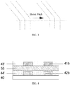
- the fanout region is provided with a first fanout line 41a and a second fanout line 42a.
- the signal line may be connected to the first fanout line 41a, or the signal line may also be connected to the second fanout line 42a, so that the signal line can realize signal transmission to the external integrated circuit through the fanout line.
- the signal line may include a first signal line connected to the first fanout line 41a and a second signal line connected to the second fanout line 42a.
- the spacer layer 55 is made of an insulating material and may be used to form a relatively large interlayer space between the first fanout line layer and the second fanout line layer.
- the orthographic projection of the first fanout line 41a on a base substrate 40 and the orthographic projection of the second fanout line 42a on the base substrate 40 are at least partially overlapped with each other.
- the array substrate shown in FIG. 2 further includes a first insulating layer 43' and a second insulating layer 44'.
- the second insulating layer 44' may also be regarded as one of the spacer layers.
- the spacer layer is provided between the first fanout line layer and the second fanout line layer so as to increase the interval space therebetween.
- the capacitance formed between the first fanout line and the second fanout line further are reduced. Therefore, the problem of crosstalk is decreased and the power consumption is lowered.
- the reduction in the capacitance formed between the first fanout line and the second fanout line also allows a certain overlap between the first fanout line and the second fanout line, thereby reducing the pitch of lines and decreasing the length of the fanout region in the Y direction which helps to narrow the frame.
- the fanout line in the fanout region usually has an inclined section and a vertical section.
- the pitch of the fanout line is reduced, the fanout lines will be compressed to the middle, and the inclined sections of the fanout lines will be compressed in both X and Y directions (refer to FIG. 1 ). In this way, the length of the fanout lines in the Y direction is reduced, so that the width of the lower frame of the array substrate could be reduced.
- the orthographic projection of the first fanout line 41b on the base substrate 40 and the orthographic projection of the corresponding second fanout line 42b on the base substrate 40 are overlapped with each other.
- the capacitance formed between the first fanout line and the second fanout line is reduced by increasing the interlayer space between layers.
- the crosstalk problem is reduced, so that the first fanout line and the second fanout line can be overlapped completely, which could further reduce the pitch of lines and thus reduce the width of the lower frame.
- the pitch of lines can be reduced by about 17% compared to the existing design, and the length of the fanout region in the Y direction can be reduced by about 20% compared to the existing design.
- the spacer layer 55 may include a buffer layer.
- a buffer layer is usually provided thereon.
- the buffer layer can prevent the impurities in the substrate from entering other layers.
- the material of the buffer layer is usually an insulating material, such as SiNx or SiOx, although it is not limited thereto.
- the buffer layer is usually located near the base substrate 40. Therefore, when the second fanout line 42e/42f/42g is located below the buffer layer and the first fanout line 41e/41f (refer to FIGS. 6A and 6B ) is located above the buffer layer, the interlayer space between the first fanout line and the second fanout line can be ensured to be large enough so that the capacitance between them can be reduced.
- a layer of light shielding material is usually provided on the base substrate 40 to form a light shielding layer.
- the light shielding layer LS is used to shield the incident light through the back of the array substrate (such as the incident light into the array substrate from the base substrate) so as to prevent the light from adversely affecting the array substrate.
- light shielding layer LS may prevent the light from illuminating the active layer of the thin film transistor (TFT) array on the array substrate, thereby avoiding the photo-induced carriers from being generated by the active layer due to the light.
- the second fanout line layer 42e, 42f or 42g is also disposed on the base substrate 40.
- the second fanout line layer 42e, 42f or 42g and the light shielding layer of the array substrate may be made of the same material and located in the same layer.
- the second fanout line layer 42e, 42f or 42g itself can be regarded as a part of the light shielding layer LS and also has a light shielding effect.
- the light shielding layer LS is usually disposed directly on the substrate such that it is the lowest layer structure. Therefore, when one of the fanout line layers and the light shielding layer LS are in the same layer, there is enough interlayer space between the one of the fanout line layers and the other one of the fanout line layers.
- the second fanout line 42e, 42f or 42g is formed by patterning the light shielding layer LS in the fanout region 20.
- the interlayer space between the one of the fanout lines and the other one of the fanout lines can be increased to further reduce the crosstalk and on the other hand, the light shielding layer (made of metal material, usually Mo) in the fanout region is more fully utilized.
- the fanout lines can be formed in the fanout region by using the same patterning process in single step.
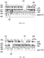
- the first gate line for forming a gate electrode of a TFT functions as the first fanout line 4 1e in the fanout region.
- the first fanout line 41e and the second fanout line 42e, 42f or 42g as shown in FIG. 5A, 5B or 5C form the fanout lines in the fanout region.
- the second gate line for forming the storage capacitor functions as the first fanout line 41f in the fanout region.
- the first fanout line 41f and the second fanout line 42e, 42f or 42g as shown in FIG. 5A, 5B or 5C form the fanout lines in the fanout region.
- the first fanout line in the fanout region is formed by the gate line, since they can be fabricated at the same time by using single patterning process at the same layer, which, however, does not mean that the first fanout line and the gate line are electrically connected with each other. It is well known that the gate line and the fanout line are usually not electrically connected with each other in order to realize respective functions.
- the first gate line or the second gate line When the first gate line or the second gate line is formed as the first fanout line, it can be used with the aforementioned second fanout line formed by patterning the light shielding layer LS so as to form the two kinds of fanout lines in the fanout region.
- the first fanout line layer where the first fanout line is located and the second fanout line layer where the second fanout line is located there is generally provided with a first buffer layer 44, a second buffer layer 45, a first gate insulating layer 46, and the like (as shown in FIG. 5B , a second gate insulating layer 47 may be included in some cases). These layers each may be part of the spacer layer.
- the thickness of layers may be used to reduce the capacitance between the first fanout line and the second fanout line, thereby avoiding signal crosstalk between the first fanout line and the second fanout line. If the capacitance between the first fanout line and the second fanout line needs to be further reduced, the thickness of the layers, such as the buffer layer and the gate insulating layer, etc., can also be appropriately increased.
- the total thickness of the one or more spacer layers may be greater than 500 nm.
- the capacitance per unit area between the first fanout line and the second fanout line which are at least partially overlapped with each other is less than 8 ⁇ 10 -5 picofarads per square micrometer. The design including the total thickness of the above-mentioned spacer layer and the capacitance per unit area can effectively prevent signal crosstalk between the first fanout line and the second fanout line.
- the first fanout line layer includes a plurality of first fanout lines
- the second fanout line layer includes a plurality of second fanout lines.
- the pitch of the plurality of first fanout lines and the pitch of the plurality of second fanout lines may be between 1.5 ⁇ m and 3.0 ⁇ m.
- the main function of the fanout region is to connect the data line 11 or the first gate line 12 of the circuit in the display region to an external integrated circuit. Therefore, the data line 11 or the first gate line 12 need to be connected to an external IC through the fanout line.
- the data line and the fanout line may be directly connected with each other through a via hole.
- the array substrate may further include a transition line layer.
- the transition line layer is disposed between the data line layer where the data line is located and the first fanout line layer.
- the transition line layer may be disposed between the data line layer where the data line is located and the second fanout line layer.
- the transition line layer includes a transition line 60a/60b, as shown in FIGS. 5A and 5B .
- the data line is connected to the first fanout line or the second fanout line though the transition line. In this way, by providing the transition line layer, the depth of the via hole can be reduced and the reliability of the electrical connection can be improved. This method is particularly beneficial to the case where the interlayer space between the light shielding layer LS and the data line layer 50 where the data line is located is relatively large and the layers structure between the light shielding layer LS and the data line layer 50 is complicated.
- the gate line which may be the first gate line 12 or the second gate line 13, is formed in the display region.
- the transition line layer and the gate line layer where the gate line is located are in the same layer. In this way, the transition line is formed at the same time by using the process of making the gate line, thereby saving process steps and improving production efficiency.
- the transition line 60a and the first gate line which is used to form the gate electrode of the TFT may be made from the same material and disposed in the same layer, and the data line 50 is connected to the second fanout line 42e through the transition line 60a.
- the corresponding transition line 60a may be formed at the boundary between the display region 10 and the fanout region 20 to electrically connect the data line 50 with the second fanout line 42e.
- the array substrate may include a first gate line layer where a first gate line is located and a second gate line layer where a second gate line is located.
- the transition line layer and the first gate line layer may be made from the same material and arranged in the same layer.
- the fanout region 20 includes: at least one buffer layer (for example, the first buffer layer 44 and/or the second buffer layer 45) and a first gate insulating layer 46 between the transition line layer where the transition line 60a is located and the second fanout line layer where the second fanout line 42e is located; and a second gate insulating layer 47 and at least one interlayer dielectric layer between the data line layer and the transition line layer.
- the data line 50 is electrically connected to the transition line 60a through a first conductive plug 61 which penetrates the second gate insulating layer 47 and at least one interlayer dielectric layer, and the transition line 60a is electrically connected to the second fanout line 42e through a second conductive plug 62 which penetrates the at least one buffer layer and the first gate insulating layer 46.
- the transition line 60b and the second gate line which is used to form the storage capacitor may be made from the same material and disposed in the same layer.
- the transition line is used for electrically connecting the data line 50 with the second fanout line 42f.
- the transition line layer 60b and the second gate line layer may be made from the same material and arranged in the same layer.
- the fanout region 20 may include: at least one buffer layer (for example, the first buffer layer 44 and/or the second buffer layer 45), a first gate insulating layer 46 and a second gate insulating layer 47 between the transition line layer where the transition line 60b is located and the second fanout line layer where the second fanout line 42e is located); and at least one interlayer dielectric layer between the data line layer and the transition line layer.
- the data line 50 is electrically connected to the transition line 60a through a third conductive plug 63 which penetrates at least one interlayer dielectric layer
- the transition line 60b is electrically connected to the second fanout line 42f through a fourth conductive plug 64 which penetrates the at least one buffer layer, the first gate insulating layer 46 and the second gate insulating layer 47.
- the data line can be directly connected to the second fanout line.
- the data line 50 and the second fanout line 42g are directly connected through the via hole.
- the data line 50 is electrically connected to the first fanout line or the second fanout line through a fifth conductive plug 65.
- the fifth conductive plug 65 penetrates one or more insulating layers between the data line layer and the first fanout line or between the data line layer and the second fanout line layer.
- the external integrated circuit is usually implemented by a separate circuit board 70, and there is a bending region 80 between the circuit board 70 and the fanout region 20.
- the bending of the bending region 80 allows the circuit board 70 to be folded back under the display region and the fanout region of the display panel, so that the circuit board 70 does not contribute to the frame width.
- the fanout region is used to provide a transition area for the connection between the display region and the external integrated circuit.
- the fanout line of the fanout region 20 needs to be connected to the data line in the bending area 80 in addition to the data line of the display region 10.
- the fanout line in the fanout region 20 and the data line in the bending region 80 may be connected with each other in any manner as shown in FIGS. 5A to 5C .
- FIGS. 5A, 5B and 5C show the connection between the data line and second fanout line formed by using the light shielding layer LS.
- FIGS. 6A and 6B show the connection between the first fanout line and the data line in the case where the first fanout line 41e and the first gate line are made of the same material and are disposed in the same layer and the first fanout line 41f and the second gate line are made of the same material and are arranged in the same layer.
- any one of the structures shown in FIGS. 5A to 5C and the structure of FIG. 6A or FIG. 6B may be used.
- FIGS. 5A to 5C mainly show the line arrangement at the boundary between the display region 10 and the fanout region 20 (i.e., the part between the two vertical dashed lines in FIGS. 5A to 5C ).
- the orthographic projection of the first fanout line on the base substrate and the orthographic projection of the second fanout line on the base substrate may be overlapped partially or even overlapped completely, as shown in FIG. 2 and FIG. 4 , which can be completely achieved through a patterning process.
- the layers structure shown in FIGS. 5A to 5C and FIGS. 6A and 6B includes the base substrate 40.
- the array substrate may further include a first buffer layer 44, a second buffer layer 45, a first gate insulating layer (GI) 46, a second gate insulating layer 47, a first interlayer dielectric layer (ILD) 43, and a second interlayer dielectric layer 48.
- GI gate insulating layer
- ILD interlayer dielectric layer
- the two buffer layers one of them is used to isolate the metal ions in the base substrate 40 made of glass to prevent the metal ions from diffusing into the TFT device, while the other one of them is used for heat preservation which would facilitate the formation of large crystalline grains of silicon (Si).
- the two interlayer dielectric layers one of them is made of SiOx for the purpose of planarization and insulation, while the other one of them is made of SiNx for the purpose of repairing Si defects.
- the first gate insulating layer 46 is used to insulate the first gate line layer (such as a metal layer) where the first gate line 12 is located, and the second gate insulating layer 47 is used to insulate the second gate line layer (such as a metal layer) where the second gate line 13 is located. It is appreciated that such a layers structure is only illustrated schematically, and does not mean that the present disclosure seeks to protect an array substrate only containing all of these layers. It is known that, if allowed, each layer in the layers structure may be increased or decreased. These deformations should also fall within the protection scope of the present disclosure.
- the present disclosure aims to make the length of the display panel in the Y direction as small as possible by balancing the lines pitch and the capacitance between the lines, thereby achieving the goal of realizing a narrow frame. Any technical solution that can achieve this goal and has substantially the same principle should be considered to belong to the protection scope of the present disclosure.
- the data line is used as an example for description.
- the gate line also needs to transmit signals with the external IC circuit through the fanout line. Therefore, the connection between the gate line and the fanout line can be realized with reference to the foregoing embodiments relating to the connection between the data line and the fanout line, and details are not described herein again.
- the array substrate including two types of gate lines (that is, the first gate line 12 and the second gate line 13) is used as an example for description.
- the principle mentioned above is also applicable, and details are not described herein again.
- An embodiment of the present disclosure also provides a display device, which can reduce the width of the frame of the display panel to a certain extent.
- the display device includes any one embodiment or combination of embodiments of the array substrate as described above.
- the spacer layer is provided between the first fanout line layer and the second fanout line layer so as to increase the interval space therebetween.
- the capacitance formed between the first fanout line and the second fanout line further are reduced. Therefore, the problem of crosstalk is decreased and the power consumption is lowered.
- the reduction in the capacitance formed between the first fanout line and the second fanout line also allow a certain overlap between the first fanout line and the second fanout line, thereby reducing the pitch of lines and decreasing the length of the fanout region in the Y direction which helps to narrow the frame.
- the display device in the present embodiments may be any product or component with display function, such as electronic paper, mobile phones, tablet computers, TVs, laptops, digital photo frames, navigators and the like.
- An embodiment of the present disclosure further provides a method of manufacturing an array substrate, which can reduce the width of the frame of the display panel to a certain extent.
- the manufacturing method of the array substrate includes:
- the spacer layer is made of an insulating material; the signal line is formed in a display region of the array substrate; and the first fanout line and the second fanout line are formed in a fanout region of the array substrate.
- the spacer layer is provided between the first fanout line layer and the second fanout line layer so as to increase the interval space between the first fanout line layer and the second fanout line layer.
- the capacitance formed between the first fanout line and the second fanout line is further reduced. Therefore, the crosstalk is decreased and the power consumption is lowered.
- the reduction in the capacitance formed between the first fanout line and the second fanout line also allows a certain overlap between the first fanout line and the second fanout line, thereby reducing the pitch of lines and decreasing the length of the fanout region in the Y direction which helps to narrow the frame.
- step 91 in the manufacturing method of the array substrate may further include the following steps:
- the layer structure between the one of the fanout line layers and the other one of the fanout line layers can be used as the spacer layer, so that the interlayer space can be increased (the light shielding layer is directly disposed on the substrate and thus belongs to the lowest layer structure) and the crosstalk may be further reduced. Meanwhile, the light shielding layer (metal material) existing in the fanout region can be fully utilized.
- the signal line further includes a gate line
- the manufacturing method of the array substrate may further include the following steps after the step 92:
- the gate line layer and the transition line layer can be formed at the same time through one patterning process, which simplifies the process and improves production efficiency.
- the gate line includes a first gate line 12 for forming a gate electrode of the TFT and a second gate line 13 for forming a storage capacitor in a display region of the array substrate. While making either the first gate line 12 or the second gate line 13, the transition line layer can be made simultaneously.
- the orthographic projection of the first fanout line and the orthographic projection of the second fanout line are overlapped with each other. Since the crosstalk is reduced, an overlap can be formed between the first fanout line and the second fanout line, which could reduce the pitch of lines and thus reduce the width of the lower frame.
- the spacer layer may include a buffer layer, or at least one gate insulating layer, or a combination of the buffer layer and at least one gate insulating layer.
- the buffer layer can prevent the impurities in the base substrate from entering other layers, and the material of the buffer layer is not limited.
- the material of the buffer layer may include for example SiNx or SiOx, although it is not limited thereto.
- the buffer layer is usually located near the base substrate. Therefore, when the second fanout line is located below the buffer layer and the first fanout line is located above the buffer layer, the interlayer space between the first fanout line and the second fanout line can be ensured to be large enough so that the capacitance between them can be reduced.
- the interlayer space between the first fanout line and the second fanout line can be increased to further reduce the crosstalk issues.
- the operations for forming the above layers include, but are not limited to (chemical phase, physical phase) deposition, and (magnetron) sputtering deposition. Those skilled in the art can understand that after forming each layer, corresponding patterns may be further formed thereon as erequired, which is not described in this disclosure any longer.
- the spacer layer is provided between the first fanout line layer and the second fanout line layer so as to increase the interval space therebetween.
- the capacitance formed between the first fanout line and the second fanout line further is reduced. Therefore, the crosstalk is decreased and the power consumption is lowered.
- the reduction in the capacitance formed between the first fanout line and the second fanout line also allows a certain overlap between the first fanout line and the second fanout line, thereby reducing the pitch of lines and decreasing the length of the fanout region in the Y direction, which helps to narrow the frame.
- the source/drain electrode and the active layer are in different layers, thus the array substrate has large thickness and the manufacturing process is complicated.
- the source electrode, drain electrode, data line, and active layer can be fabricated in the same layer by doping the copper nitride, thereby reducing the thickness of the array substrate and simplifying the fabricating process of the array substrate.
Landscapes
- Devices For Indicating Variable Information By Combining Individual Elements (AREA)
- Liquid Crystal (AREA)
- Engineering & Computer Science (AREA)
- Manufacturing & Machinery (AREA)
Abstract
Description
- This application claims the benefit of
Chinese Patent Application No.201811486997.0 filed on December 6, 2018 - The present disclosure relates to the field of display technology, and more specifically, to an array substrate and its manufacturing method and a display device.
- Currently, it is one of the tendencies of a display panel to narrow its lower frame and increase the screen-to-body ratio. In the existing design, after the bending process during the module (MDL) process, the main constituent component of the lower frame of the display panel is a fanout region, which accounts for 64% of the entire area of the lower frame of the display panel. In order to reduce the width of the lower frame of the display panel, it is necessary to reduce the pitch between the fanout lines so as to decrease the length of fanout region in the Y direction.
- An embodiment of the present application provides an array substrate, including: a base substrate; and a display region and a fanout region on the base substrate, wherein a signal line is provided in the display region; the fanout region includes a first fanout line layer in which a first fanout line is provided, a second fanout line layer in which a second fanout line is provided, and one or more spacer layers between the first fanout line layer and the second fanout line layer; the signal line is connected to the first fanout line or the second fanout line; and the spacer layers are made of an insulating material; wherein an orthographic projection of the first fanout line on the base substrate and an orthographic projection of the second fanout line on the base substrate are at least partially overlapped with each other.
- In some embodiments, the signal line includes a first signal line connected to the first fanout line and a second signal line connected to the second fanout line.
- In some embodiments, the array substrate includes a light shielding layer which is configured to shield incident light into the array substrate from the base substrate, and the second fanout line layer and the light shielding layer of the array substrate are made of same material and are in one same layer.
- In some embodiments, the array substrate includes at least one gate line layers, and the first fanout line layer and one of the at least one gate line layers are made of same material and are in one same layer.
- In some embodiments, the signal line includes a data line; the array substrate further includes a data line layer in which the data line is provided and a transition line layer between the data line layer and the first fanout line layer or between the data line layer and the second fanout line layer; the transition line layer includes a transition line; and the data line is electrically connected to the transition line and the transition line is electrically connected to the first fanout line or the second fanout line.
- In some embodiments, the signal line further includes a gate line, and the transition line layer and the gate line are made of same material and are in one same layer.
- In some embodiments, the array substrate includes a first gate line layer and a second gate line layer; the transition line layer and the first gate line layer are made of same material and are in one same layer; the fanout region includes at least one buffer layer and a first gate insulating layer between the transition line layer and the second fanout line layer, and a second gate insulating layer and at least one interlayer dielectric layer between the data line layer and the transition line layer; the data line is electrically connected to the transition line through a first conductive plug which penetrates the second gate insulating layer and the at least one interlayer dielectric layer; and the transition line is electrically connected to the second fanout line through a second conductive plug which penetrates the at least one buffer layer and the first gate insulating layer.
- In some embodiments, the array substrate includes a first gate line layer and a second gate line layer; the transition line layer and the second gate line layer are made of same material and are in one same layer; the fanout region includes at least one buffer layer, a first gate insulating layer, and a second gate insulating layer between the transition line layer and the second fanout line layer, and at least one interlayer dielectric layer between the data line layer and the transition line layer; the data line is electrically connected to the transition line through a third conductive plug which penetrates the at least one interlayer dielectric layer; and the transition line is electrically connected to the second fanout line through a fourth conductive plug which penetrates the at least one buffer layer, the first gate insulating layer and the second gate insulating layer.
- In some embodiments, the signal line includes a data line; the array substrate further includes a data line layer in which the data line is provided; the data line is electrically connected to the first fanout line or the second fanout line through a fifth conductive plug which penetrates one or more insulating layers between the data line layer and the first fanout line or between the data line layer and the second fanout line layer.
- In some embodiments, the orthographic projection of the first fanout line on the base substrate and the orthographic projection of the second fanout line on the base substrate are fully overlapped with each other.
- In some embodiments, the spacer layers include a buffer layer, or at least one gate insulating layer, or a combination of the buffer layer and the at least one gate insulating layer.
- In some embodiments, a total thickness of the one or more spacer layers is greater than 500 nm.
- In some embodiments, the first fanout line layer includes a plurality of the first fanout lines, and the second fanout line layer includes a plurality of the second fanout lines; and each of a pitch of the plurality of first fanout lines and a pitch of the plurality of second fanout lines is between 1.5 µm and 3.0µm.
- In some embodiments, a capacitance per unit area between the first fanout line and the second fanout line which are at least partially overlapped with each other is less than 8×10⁻⁵ picofarad per square micrometer.
- An embodiment of the present disclosure also provides a display device including the array substrate as described in any one of the above embodiments.
- An embodiment of the present disclosure also provides a method of manufacturing an array substrate, including: forming a second fanout line layer including a second fanout line on a base substrate; forming one or more spacer layers on a side of the second fanout line layer distal to the base substrate; forming a first fanout line layer including a first fanout line on a side of the spacer layers distal to the base substrate, an orthographic projection of the first fanout line on the base substrate and an orthographic projection of the second fanout line on the base substrate being at least partially overlapped with each other; forming a signal line layer including a signal line on a side of the first fanout line layer distal to the base substrate, the signal line being connected to the first fanout line or the second fanout line; wherein, the spacer layers are made of an insulating material; the signal line is formed in a display region of the array substrate; and the first fanout line and the second fanout line are formed in a fanout region of the array substrate.
- In some embodiments, the step of forming the second fanout line layer including the second fanout line on the base substrate further includes: forming a first metal thin film on the base substrate; and patterning the first metal thin film to form a light shielding layer and the second fanout line layer, the light shielding layer shielding incident light into the array substrate from the base substrate.
- In some embodiments, the signal line includes a gate line, and after the step of forming one or more spacer layers on the side of the second fanout line layer distal to the base substrate, the method further includes: forming a second metal thin film on the spacer layers; patterning the second metal thin film to form a gate line layer in the display region and form a transition line layer at a boundary between the display region and the fanout region.
- In some embodiments, the orthographic projection of the first fanout line on the base substrate and the orthographic projection of the second fanout line on the base substrate are fully overlapped with each other.
- In some embodiments, the spacer layers include: a buffer layer, or at least one gate insulating layer, or a combination of the buffer layer and the at least one gate insulating layer.
- In order to further clarify the technical solutions of the embodiments of the present disclosure, the drawings of the embodiments will be briefly described below. Obviously, the drawings described below only relate to some embodiments of the present disclosure instead of limiting the present disclosure.
-
Fig. 1 schematically illustrates an array substrate according to some embodiments of the present disclosure; -
Fig. 2 schematically illustrates the cross-sectional view of a fanout region of an array substrate taken along the line AA' inFIG. 1 according to some embodiments of the present disclosure; -
FIG. 3 schematically illustrates the principle of shrinking pitch of traces to narrow the lower frame in the Y direction; -
Fig. 4 schematically illustrates the cross-sectional view of a fanout region of an array substrate taken along the line AA' inFIG. 1 according to some other embodiments of the present disclosure; -
Fig. 5A schematically illustrates the cross-sectional view of a fanout region of an array substrate taken along the line BB' inFIG. 1 according to some other embodiments of the present disclosure; -
Fig. 5B schematically illustrates the cross-sectional view of a fanout region of an array substrate taken along the line BB' inFIG. 1 according to still other embodiments of the present disclosure; -
Fig. 5C schematically illustrates the cross-sectional view of a fanout region of an array substrate taken along the line BB' inFIG. 1 according to yet other embodiments of the present disclosure; -
Fig. 6A schematically illustrates the cross-sectional view of a fanout region of an array substrate taken along the line BB' inFIG. 1 according to some other embodiments of the present disclosure; -
Fig. 6B schematically illustrates the cross-sectional view of a fanout region of an array substrate taken along the line BB' inFIG. 1 according to still other embodiments of the present disclosure; and -
FIG. 7 schematically illustrates a flowchart of a method of manufacturing an array substrate according to some embodiments of the present disclosure. - In order to make the purpose, technical solutions and advantages of the embodiments of the present disclosure clearer, the technical solution of the embodiments of the present disclosure will be described clearly and completely below in conjunction with the accompanying drawings of the embodiments of the present disclosure. It is obvious that the described embodiments are a part of the embodiments of the present disclosure rather than all the embodiments of the present disclosure. Based on the described embodiments of the present disclosure, those skilled in the art can obtain other embodiments, without any inventive efforts, which should fall within the scope of the present disclosure.
- Unless otherwise defined, technical terms or scientific terms used in the present disclosure are intended to be understood as having the ordinary meaning for those skilled in the art. The words "first", "second" and the like used in the present disclosure are not intended to define order, number, or priority, but to distinguish different components. Similarly, "a/an", "one", or "the" and the like do not indicate a limit on quantity, but rather indicates that there is at least one. The word "comprising" or "including" and the like mean that the element or item before the word is intended to encompass the element, the item and the like recited after the word, and not exclude other element or item. The word "connect" or "couple" and the like are not limited to physical or mechanical connections, but may include electrical connections, including direct or indirect connections. The words "upper", "lower", "left", "right", and the like are only used to indicate relative positional relationship. When the position of the described object changes, the relative positional relationship may also change accordingly.
- An embodiment of the present disclosure provides an array substrate, which can reduce the width of the frame of the display panel to a certain extent.
-
FIG. 1 schematically illustrates an array substrate. The array substrate includes adisplay region 10 and afanout region 20. There are signal lines formed in the display region. The signal lines include adata line 11, afirst gate line 12, and a second gate line 13. Thedata line 11 is used to input the driving signal. Thefirst gate line 12 is for example connected to the gate electrode of the thin film transistor (TFT) to provide a scanning signal. The second gate line 13 is used to, for example, form a storage capacitor. The signal transmission between the signal lines in thedisplay region 10 and the external integrated circuit (IC) can be realized for example through the fanout lines in thefanout region 20. - The external integrated circuit is usually implemented by a
separate circuit board 70, and there is a bendingregion 80 between thecircuit board 70 and thefanout region 20. The bending of the bendingregion 80 allows thecircuit board 70 to be folded back under the display region and the fanout region of the display panel, so that thecircuit board 70 does not contribute to the frame width. -
FIG. 2 is a cross-sectional view of thefanout region 20 taken along the line AA' inFIG. 1 . As shown inFIG. 2 , the fanout region is provided with afirst fanout line 41a and asecond fanout line 42a. The signal line may be connected to thefirst fanout line 41a, or the signal line may also be connected to thesecond fanout line 42a, so that the signal line can realize signal transmission to the external integrated circuit through the fanout line. In some embodiments, the signal line may include a first signal line connected to thefirst fanout line 41a and a second signal line connected to thesecond fanout line 42a. Between the first fanout line layer where thefirst fanout line 41a is located and the second fanout line layer where thesecond fanout line 42a is located, there may be provided with one or more spacer layers 55. Thespacer layer 55 is made of an insulating material and may be used to form a relatively large interlayer space between the first fanout line layer and the second fanout line layer. The orthographic projection of thefirst fanout line 41a on abase substrate 40 and the orthographic projection of thesecond fanout line 42a on thebase substrate 40 are at least partially overlapped with each other. The array substrate shown inFIG. 2 further includes a first insulating layer 43' and a second insulating layer 44'. The second insulating layer 44' may also be regarded as one of the spacer layers. - As can be seen from the above embodiments, in the array substrate provided by the present disclosure, the spacer layer is provided between the first fanout line layer and the second fanout line layer so as to increase the interval space therebetween. Thus, the capacitance formed between the first fanout line and the second fanout line further are reduced. Therefore, the problem of crosstalk is decreased and the power consumption is lowered. Meanwhile, the reduction in the capacitance formed between the first fanout line and the second fanout line also allows a certain overlap between the first fanout line and the second fanout line, thereby reducing the pitch of lines and decreasing the length of the fanout region in the Y direction which helps to narrow the frame.
- The relationship between the reduction of the lines pitch and the realization of the narrow frame will be described briefly with reference to
FIGS. 1 and3 . As shown inFig. 3 , the fanout line in the fanout region usually has an inclined section and a vertical section. When the pitch of the fanout line is reduced, the fanout lines will be compressed to the middle, and the inclined sections of the fanout lines will be compressed in both X and Y directions (refer toFIG. 1 ). In this way, the length of the fanout lines in the Y direction is reduced, so that the width of the lower frame of the array substrate could be reduced. - As some embodiments of the present disclosure, as shown in
FIG. 4 , the orthographic projection of thefirst fanout line 41b on thebase substrate 40 and the orthographic projection of the correspondingsecond fanout line 42b on thebase substrate 40 are overlapped with each other. The capacitance formed between the first fanout line and the second fanout line is reduced by increasing the interlayer space between layers. Thus, the crosstalk problem is reduced, so that the first fanout line and the second fanout line can be overlapped completely, which could further reduce the pitch of lines and thus reduce the width of the lower frame. Through overlapping the fanout lines, for example, the pitch of lines can be reduced by about 17% compared to the existing design, and the length of the fanout region in the Y direction can be reduced by about 20% compared to the existing design. - As some embodiments of the present disclosure, referring to
FIG. 5A, FIG. 5B , andFIG. 5C , thespacer layer 55 may include a buffer layer. When thebase substrate 40 is made of glass, a buffer layer is usually provided thereon. The buffer layer can prevent the impurities in the substrate from entering other layers. The material of the buffer layer is usually an insulating material, such as SiNx or SiOx, although it is not limited thereto. The buffer layer is usually located near thebase substrate 40. Therefore, when thesecond fanout line 42e/42f/42g is located below the buffer layer and thefirst fanout line 41e/41f (refer toFIGS. 6A and6B ) is located above the buffer layer, the interlayer space between the first fanout line and the second fanout line can be ensured to be large enough so that the capacitance between them can be reduced. - As an embodiment of the present disclosure, referring to
FIG. 5A, 5B , or5C , a layer of light shielding material is usually provided on thebase substrate 40 to form a light shielding layer. The light shielding layer LS is used to shield the incident light through the back of the array substrate (such as the incident light into the array substrate from the base substrate) so as to prevent the light from adversely affecting the array substrate. For example, light shielding layer LS may prevent the light from illuminating the active layer of the thin film transistor (TFT) array on the array substrate, thereby avoiding the photo-induced carriers from being generated by the active layer due to the light. It can be seen that the secondfanout line layer base substrate 40. That is, the secondfanout line layer fanout line layer - In some embodiments, when the light shielding layer is made of a metal material, the
second fanout line fanout region 20. Through fabricating one of the fanout line layers by the light shielding layer LS, on one hand, the interlayer space between the one of the fanout lines and the other one of the fanout lines can be increased to further reduce the crosstalk and on the other hand, the light shielding layer (made of metal material, usually Mo) in the fanout region is more fully utilized. - As some embodiments of the present disclosure, as shown in
FIG. 1 , in the display region of the array substrate there is provided with afirst gate line 12 for forming a gate electrode of a thin film transistor (TFT) and a second gate line 13 for forming a storage capacitor. While fabricating these two kinds of gate lines, the fanout lines can be formed in the fanout region by using the same patterning process in single step. As shown inFIG. 6A , the first gate line for forming a gate electrode of a TFT functions as the first fanout line 4 1e in the fanout region. Thefirst fanout line 41e and thesecond fanout line FIG. 5A, 5B or5C form the fanout lines in the fanout region. As shown inFIG. 6B , the second gate line for forming the storage capacitor functions as thefirst fanout line 41f in the fanout region. Thefirst fanout line 41f and thesecond fanout line FIG. 5A, 5B or5C form the fanout lines in the fanout region. It should be noted that, the first fanout line in the fanout region is formed by the gate line, since they can be fabricated at the same time by using single patterning process at the same layer, which, however, does not mean that the first fanout line and the gate line are electrically connected with each other. It is well known that the gate line and the fanout line are usually not electrically connected with each other in order to realize respective functions. - When the first gate line or the second gate line is formed as the first fanout line, it can be used with the aforementioned second fanout line formed by patterning the light shielding layer LS so as to form the two kinds of fanout lines in the fanout region. Between the first fanout line layer where the first fanout line is located and the second fanout line layer where the second fanout line is located, there is generally provided with a
first buffer layer 44, asecond buffer layer 45, a firstgate insulating layer 46, and the like (as shown inFIG. 5B , a secondgate insulating layer 47 may be included in some cases). These layers each may be part of the spacer layer. In this way, the thickness of layers, such as the buffer layer, the gate insulating layer, etc., may be used to reduce the capacitance between the first fanout line and the second fanout line, thereby avoiding signal crosstalk between the first fanout line and the second fanout line. If the capacitance between the first fanout line and the second fanout line needs to be further reduced, the thickness of the layers, such as the buffer layer and the gate insulating layer, etc., can also be appropriately increased. - In some embodiments, the total thickness of the one or more spacer layers may be greater than 500 nm. In some embodiments, the capacitance per unit area between the first fanout line and the second fanout line which are at least partially overlapped with each other is less than 8×10⁻⁵ picofarads per square micrometer. The design including the total thickness of the above-mentioned spacer layer and the capacitance per unit area can effectively prevent signal crosstalk between the first fanout line and the second fanout line.
- In some embodiments, the first fanout line layer includes a plurality of first fanout lines, and the second fanout line layer includes a plurality of second fanout lines. The pitch of the plurality of first fanout lines and the pitch of the plurality of second fanout lines may be between 1.5µm and 3.0µm. In general, the main function of the fanout region is to connect the
data line 11 or thefirst gate line 12 of the circuit in the display region to an external integrated circuit. Therefore, thedata line 11 or thefirst gate line 12 need to be connected to an external IC through the fanout line. In the embodiment of the present disclosure, when one of the fanout line layers is made by means of the light shielding layer LS, the data line and the fanout line may be directly connected with each other through a via hole. - In some embodiments, the array substrate may further include a transition line layer. The transition line layer is disposed between the data line layer where the data line is located and the first fanout line layer. Alternatively, the transition line layer may be disposed between the data line layer where the data line is located and the second fanout line layer. The transition line layer includes a
transition line 60a/60b, as shown inFIGS. 5A and 5B . The data line is connected to the first fanout line or the second fanout line though the transition line. In this way, by providing the transition line layer, the depth of the via hole can be reduced and the reliability of the electrical connection can be improved. This method is particularly beneficial to the case where the interlayer space between the light shielding layer LS and thedata line layer 50 where the data line is located is relatively large and the layers structure between the light shielding layer LS and thedata line layer 50 is complicated. - According to some embodiments of the present disclosure, the gate line, which may be the
first gate line 12 or the second gate line 13, is formed in the display region. The transition line layer and the gate line layer where the gate line is located are in the same layer. In this way, the transition line is formed at the same time by using the process of making the gate line, thereby saving process steps and improving production efficiency. - As shown in
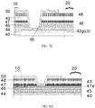
FIG. 5A , at the boundary between thedisplay region 10 and the fanout region 20 (i.e., the region between the two vertical dashed lines inFIG. 5A ), thetransition line 60a and the first gate line which is used to form the gate electrode of the TFT may be made from the same material and disposed in the same layer, and thedata line 50 is connected to thesecond fanout line 42e through thetransition line 60a. As the gate is formed in the display region, thecorresponding transition line 60a may be formed at the boundary between thedisplay region 10 and thefanout region 20 to electrically connect thedata line 50 with thesecond fanout line 42e. In some embodiments, the array substrate may include a first gate line layer where a first gate line is located and a second gate line layer where a second gate line is located. The transition line layer and the first gate line layer may be made from the same material and arranged in the same layer. Thefanout region 20 includes: at least one buffer layer (for example, thefirst buffer layer 44 and/or the second buffer layer 45) and a firstgate insulating layer 46 between the transition line layer where thetransition line 60a is located and the second fanout line layer where thesecond fanout line 42e is located; and a secondgate insulating layer 47 and at least one interlayer dielectric layer between the data line layer and the transition line layer. Thedata line 50 is electrically connected to thetransition line 60a through a firstconductive plug 61 which penetrates the secondgate insulating layer 47 and at least one interlayer dielectric layer, and thetransition line 60a is electrically connected to thesecond fanout line 42e through a secondconductive plug 62 which penetrates the at least one buffer layer and the firstgate insulating layer 46. - As shown in
FIG. 5B , at the boundary between thedisplay region 10 and the fanout region 20 (i.e., the region between the two vertical dashed lines inFIG. 5B ), thetransition line 60b and the second gate line which is used to form the storage capacitor may be made from the same material and disposed in the same layer. The transition line is used for electrically connecting thedata line 50 with thesecond fanout line 42f. In some embodiments, thetransition line layer 60b and the second gate line layer may be made from the same material and arranged in the same layer. Thefanout region 20 may include: at least one buffer layer (for example, thefirst buffer layer 44 and/or the second buffer layer 45), a firstgate insulating layer 46 and a secondgate insulating layer 47 between the transition line layer where thetransition line 60b is located and the second fanout line layer where thesecond fanout line 42e is located); and at least one interlayer dielectric layer between the data line layer and the transition line layer. Thedata line 50 is electrically connected to thetransition line 60a through a thirdconductive plug 63 which penetrates at least one interlayer dielectric layer, and thetransition line 60b is electrically connected to thesecond fanout line 42f through a fourthconductive plug 64 which penetrates the at least one buffer layer, the firstgate insulating layer 46 and the secondgate insulating layer 47. - Certainly, if the stability of the direct connection between the data line and the second fanout line through a via hole can be ensured, the data line can be directly connected to the second fanout line. As shown in
FIG. 5C , thedata line 50 and thesecond fanout line 42g are directly connected through the via hole. In some embodiments, thedata line 50 is electrically connected to the first fanout line or the second fanout line through a fifthconductive plug 65. The fifthconductive plug 65 penetrates one or more insulating layers between the data line layer and the first fanout line or between the data line layer and the second fanout line layer. - It should be noted that, as shown in
FIG. 1 , the external integrated circuit is usually implemented by aseparate circuit board 70, and there is a bendingregion 80 between thecircuit board 70 and thefanout region 20. The bending of the bendingregion 80 allows thecircuit board 70 to be folded back under the display region and the fanout region of the display panel, so that thecircuit board 70 does not contribute to the frame width. The fanout region is used to provide a transition area for the connection between the display region and the external integrated circuit. Thus, in order to realize the signal transmission between the display region and the data lines of the external circuit, the fanout line of thefanout region 20 needs to be connected to the data line in the bendingarea 80 in addition to the data line of thedisplay region 10. The fanout line in thefanout region 20 and the data line in the bendingregion 80 may be connected with each other in any manner as shown inFIGS. 5A to 5C . -
FIGS. 5A, 5B and5C show the connection between the data line and second fanout line formed by using the light shielding layer LS.FIGS. 6A and6B show the connection between the first fanout line and the data line in the case where thefirst fanout line 41e and the first gate line are made of the same material and are disposed in the same layer and thefirst fanout line 41f and the second gate line are made of the same material and are arranged in the same layer. When specifically implementing the fanout line arrangement structure of the fanout region of the present disclosure, any one of the structures shown inFIGS. 5A to 5C and the structure ofFIG. 6A orFIG. 6B may be used. - It should be noted that
FIGS. 5A to 5C mainly show the line arrangement at the boundary between thedisplay region 10 and the fanout region 20 (i.e., the part between the two vertical dashed lines inFIGS. 5A to 5C ). After the data line and the fanout line are connected, in the main part of the fanout region, the orthographic projection of the first fanout line on the base substrate and the orthographic projection of the second fanout line on the base substrate may be overlapped partially or even overlapped completely, as shown inFIG. 2 andFIG. 4 , which can be completely achieved through a patterning process. - It should also be noted that the layers structure shown in
FIGS. 5A to 5C andFIGS. 6A and6B includes thebase substrate 40. Depending on the selection of the manufacturing process of the array substrate, the array substrate may further include afirst buffer layer 44, asecond buffer layer 45, a first gate insulating layer (GI) 46, a secondgate insulating layer 47, a first interlayer dielectric layer (ILD) 43, and a secondinterlayer dielectric layer 48. For the two buffer layers, one of them is used to isolate the metal ions in thebase substrate 40 made of glass to prevent the metal ions from diffusing into the TFT device, while the other one of them is used for heat preservation which would facilitate the formation of large crystalline grains of silicon (Si). For the two interlayer dielectric layers, one of them is made of SiOx for the purpose of planarization and insulation, while the other one of them is made of SiNx for the purpose of repairing Si defects. The firstgate insulating layer 46 is used to insulate the first gate line layer (such as a metal layer) where thefirst gate line 12 is located, and the secondgate insulating layer 47 is used to insulate the second gate line layer (such as a metal layer) where the second gate line 13 is located. It is appreciated that such a layers structure is only illustrated schematically, and does not mean that the present disclosure seeks to protect an array substrate only containing all of these layers. It is known that, if allowed, each layer in the layers structure may be increased or decreased. These deformations should also fall within the protection scope of the present disclosure. - Based on the descriptions of the foregoing embodiments, it should also be pointed out that the present disclosure aims to make the length of the display panel in the Y direction as small as possible by balancing the lines pitch and the capacitance between the lines, thereby achieving the goal of realizing a narrow frame. Any technical solution that can achieve this goal and has substantially the same principle should be considered to belong to the protection scope of the present disclosure.
- It should be noted that in some of the foregoing embodiments, the data line is used as an example for description. However, it is known that the gate line also needs to transmit signals with the external IC circuit through the fanout line. Therefore, the connection between the gate line and the fanout line can be realized with reference to the foregoing embodiments relating to the connection between the data line and the fanout line, and details are not described herein again.
- It should also be noted that in the foregoing embodiment, the array substrate including two types of gate lines (that is, the
first gate line 12 and the second gate line 13) is used as an example for description. However, it is known that there is a kind of array substrate that only includes one type of gate line (that is, only the gate line for receiving the scanning signal). For this kind of array substrate, the principle mentioned above is also applicable, and details are not described herein again. - An embodiment of the present disclosure also provides a display device, which can reduce the width of the frame of the display panel to a certain extent. The display device includes any one embodiment or combination of embodiments of the array substrate as described above.
- As can be seen from the above embodiments, in the display device provided by the present disclosure, the spacer layer is provided between the first fanout line layer and the second fanout line layer so as to increase the interval space therebetween. Thus, the capacitance formed between the first fanout line and the second fanout line further are reduced. Therefore, the problem of crosstalk is decreased and the power consumption is lowered. Meanwhile, the reduction in the capacitance formed between the first fanout line and the second fanout line also allow a certain overlap between the first fanout line and the second fanout line, thereby reducing the pitch of lines and decreasing the length of the fanout region in the Y direction which helps to narrow the frame.
- It is noted that, the display device in the present embodiments may be any product or component with display function, such as electronic paper, mobile phones, tablet computers, TVs, laptops, digital photo frames, navigators and the like.
- An embodiment of the present disclosure further provides a method of manufacturing an array substrate, which can reduce the width of the frame of the display panel to a certain extent.
- As shown in
FIG. 7 , the manufacturing method of the array substrate includes: - Step 91: forming a second fanout line layer including a second fanout line on a base substrate;
- Step 92: forming one or more spacer layers on a side of the second fanout line layer distal to the base substrate;
- Step 93: forming a first fanout line layer including a first fanout line on a side of the spacer layer distal to the substrate, the orthographic projection of the second fanout line on the base substrate and the orthographic projection of the first fanout line on the base substrate being at least partially overlapped with each other;
- Step 94: forming a signal line layer including a signal line on a side of the first fanout line layer distal to the base substrate, the signal line being connected to the first fanout line or the second fanout line.
- The spacer layer is made of an insulating material; the signal line is formed in a display region of the array substrate; and the first fanout line and the second fanout line are formed in a fanout region of the array substrate.
- As can be seen from the above embodiments, in the method of manufacturing the array substrate provided by the present disclosure, the spacer layer is provided between the first fanout line layer and the second fanout line layer so as to increase the interval space between the first fanout line layer and the second fanout line layer. Thus, the capacitance formed between the first fanout line and the second fanout line is further reduced. Therefore, the crosstalk is decreased and the power consumption is lowered. Meanwhile, the reduction in the capacitance formed between the first fanout line and the second fanout line also allows a certain overlap between the first fanout line and the second fanout line, thereby reducing the pitch of lines and decreasing the length of the fanout region in the Y direction which helps to narrow the frame.
- In some embodiments,
step 91 in the manufacturing method of the array substrate may further include the following steps: - forming a first metal thin film on the base substrate; and
- patterning the first metal thin film to form a light shielding layer and the second fanout line layer, wherein, the light shielding layer is used to shield the incident light into the array substrate from the base substrate, for example, to prevent the light from illuminating the active layer in a thin film transistor array of the array substrate.
- Through fabricating one of the fanout line layers by the material of the light shielding layer, the layer structure between the one of the fanout line layers and the other one of the fanout line layers can be used as the spacer layer, so that the interlayer space can be increased (the light shielding layer is directly disposed on the substrate and thus belongs to the lowest layer structure) and the crosstalk may be further reduced. Meanwhile, the light shielding layer (metal material) existing in the fanout region can be fully utilized.
- In some embodiments, the signal line further includes a gate line, and the manufacturing method of the array substrate may further include the following steps after the step 92:
- forming a second metal thin film on the spacer layer; and
- patterning the second metal thin film to form a gate line layer in the display region and form a transition line layer at the boundary between the display region and the fanout region.
- In this way, the gate line layer and the transition line layer can be formed at the same time through one patterning process, which simplifies the process and improves production efficiency.
- In some embodiments, the gate line includes a
first gate line 12 for forming a gate electrode of the TFT and a second gate line 13 for forming a storage capacitor in a display region of the array substrate. While making either thefirst gate line 12 or the second gate line 13, the transition line layer can be made simultaneously. - In some embodiments, the orthographic projection of the first fanout line and the orthographic projection of the second fanout line are overlapped with each other. Since the crosstalk is reduced, an overlap can be formed between the first fanout line and the second fanout line, which could reduce the pitch of lines and thus reduce the width of the lower frame.
- In some embodiments, the spacer layer may include a buffer layer, or at least one gate insulating layer, or a combination of the buffer layer and at least one gate insulating layer. When the substrate is made of glass, the buffer layer can prevent the impurities in the base substrate from entering other layers, and the material of the buffer layer is not limited. The material of the buffer layer may include for example SiNx or SiOx, although it is not limited thereto. The buffer layer is usually located near the base substrate. Therefore, when the second fanout line is located below the buffer layer and the first fanout line is located above the buffer layer, the interlayer space between the first fanout line and the second fanout line can be ensured to be large enough so that the capacitance between them can be reduced.
- In the embodiment of the present disclosure, by adding at least one insulating layer between the first fanout line and the second fanout line, the interlayer space between the first fanout line and the second fanout line can be increased to further reduce the crosstalk issues.
- It should be noted that the operations for forming the above layers include, but are not limited to (chemical phase, physical phase) deposition, and (magnetron) sputtering deposition. Those skilled in the art can understand that after forming each layer, corresponding patterns may be further formed thereon as erequired, which is not described in this disclosure any longer.
- As can be seen from the above embodiments, in the array substrate and its manufacturing method and the display device provided by the present disclosure, the spacer layer is provided between the first fanout line layer and the second fanout line layer so as to increase the interval space therebetween. Thus, the capacitance formed between the first fanout line and the second fanout line further is reduced. Therefore, the crosstalk is decreased and the power consumption is lowered. Meanwhile, the reduction in the capacitance formed between the first fanout line and the second fanout line also allows a certain overlap between the first fanout line and the second fanout line, thereby reducing the pitch of lines and decreasing the length of the fanout region in the Y direction, which helps to narrow the frame.
- The technical solution of the present disclosure has been described in detail above with reference to the accompanying drawings. In the prior art, the source/drain electrode and the active layer are in different layers, thus the array substrate has large thickness and the manufacturing process is complicated. In the technical solution of this application, the source electrode, drain electrode, data line, and active layer can be fabricated in the same layer by doping the copper nitride, thereby reducing the thickness of the array substrate and simplifying the fabricating process of the array substrate.
- It is noted that, in the drawings, the dimensions of layers and areas may be exaggerated for clarity of the illustration. It is appreciated that when an element or layer is referred to as being "on" another element or layer, it may be directly on another element or layer, or an intermediate layer may be present therebetween. In addition, it is understood that when an element or layer is referred to as being "under" another element or layer, it may be directly under another element or layer, or at least one intermediate layer may be present therebetween. In addition, it is understood that when a layer or element is referred to as being "between" two layers or two elements, it may be the only one layer or element between two layers or two elements, or more than one intermediate layer or element may also be present therebetween. Like reference numerals refer to like elements throughout the description.
- Those skilled in the art should understand that the foregoing descriptions are merely specific embodiments of the present disclosure and are not intended to limit the present disclosure, and any modifications, equivalent replacements, and improvements made within the spirit and principle of the present disclosure should fall within the protection scope of the present disclosure.
Claims (20)
- An array substrate, comprising:a base substrate; anda display region and a fanout region on the base substrate, wherein a signal line is provided in the display region; the fanout region comprises a first fanout line layer in which a first fanout line is provided, a second fanout line layer in which a second fanout line is provided, and one or more spacer layers between the first fanout line layer and the second fanout line layer; the signal line is connected to the first fanout line or the second fanout line; and the spacer layers are made of an insulating material;wherein an orthographic projection of the first fanout line on the base substrate and an orthographic projection of the second fanout line on the base substrate are at least partially overlapped with each other.
- The array substrate according to claim 1, wherein the signal line comprises a first signal line connected to the first fanout line and a second signal line connected to the second fanout line.
- The array substrate according to claim 1, wherein the array substrate comprises a light shielding layer which is configured to shield incident light into the array substrate from the base substrate, and the second fanout line layer and the light shielding layer of the array substrate are made of same material and are in one same layer.
- The array substrate according to claim 3, wherein the array substrate comprises at least one gate line layers, and the first fanout line layer and one of the at least one gate line layers are made of same material and are in one same layer.
- The array substrate according to claim 3, wherein, the signal line comprises a data line; the array substrate further comprises a data line layer in which the data line is provided and a transition line layer between the data line layer and the first fanout line layer or between the data line layer and the second fanout line layer; the transition line layer comprises a transition line; and the data line is electrically connected to the transition line and the transition line is electrically connected to the first fanout line or the second fanout line.
- The array substrate according to claim 5, wherein the signal line further comprises a gate line, and the transition line layer and the gate line are made of same material and are in one same layer.
- The array substrate according to claim 5, wherein, the array substrate comprises a first gate line layer and a second gate line layer; the transition line layer and the first gate line layer are made of same material and are in one same layer;the fanout region comprises at least one buffer layer and a first gate insulating layer between the transition line layer and the second fanout line layer, and a second gate insulating layer and at least one interlayer dielectric layer between the data line layer and the transition line layer;the data line is electrically connected to the transition line through a first conductive plug which penetrates the second gate insulating layer and the at least one interlayer dielectric layer; andthe transition line is electrically connected to the second fanout line through a second conductive plug which penetrates the at least one buffer layer and the first gate insulating layer.
- The array substrate according to claim 5, wherein, the array substrate comprises a first gate line layer and a second gate line layer; the transition line layer and the second gate line layer are made of same material and are in one same layer;the fanout region comprises at least one buffer layer, a first gate insulating layer, and a second gate insulating layer between the transition line layer and the second fanout line layer, and at least one interlayer dielectric layer between the data line layer and the transition line layer;the data line is electrically connected to the transition line through a third conductive plug which penetrates the at least one interlayer dielectric layer; andthe transition line is electrically connected to the second fanout line through a fourth conductive plug which penetrates the at least one buffer layer, the first gate insulating layer and the second gate insulating layer.
- The array substrate according to claim 3, wherein the signal line comprises a data line; the array substrate further comprises a data line layer in which the data line is provided; the data line is electrically connected to the first fanout line or the second fanout line through a fifth conductive plug which penetrates one or more insulating layers between the data line layer and the first fanout line or between the data line layer and the second fanout line layer.
- The array substrate according to any one of claims 1 to 9, wherein the orthographic projection of the first fanout line on the base substrate and the orthographic projection of the second fanout line on the base substrate are fully overlapped with each other.
- The array substrate according to any one of claims 1 to 9, wherein the spacer layers comprise a buffer layer, or at least one gate insulating layer, or a combination of the buffer layer and the at least one gate insulating layer.
- The array substrate according to any one of claims 1 to 9, wherein a total thickness of the one or more spacer layers is greater than 500 nm.
- The array substrate according to any one of claims 1 to 9, wherein the first fanout line layer comprises a plurality of the first fanout lines, and the second fanout line layer comprises a plurality of the second fanout lines; and each of a pitch of the plurality of first fanout lines and a pitch of the plurality of second fanout lines is between 1.5 µm and 3.0µm .
- The array substrate according to any one of claims 1 to 9, wherein a capacitance per unit area between the first fanout line and the second fanout line which are at least partially overlapped with each other is less than 8×10⁻⁵ picofarad per square micrometer.
- A display device comprising the array substrate according to any one of claims 1 to 14.
- A method of manufacturing an array substrate, comprising:forming a second fanout line layer comprising a second fanout line on a base substrate;forming one or more spacer layers on a side of the second fanout line layer distal to the base substrate;forming a first fanout line layer comprising a first fanout line on a side of the spacer layers distal to the base substrate, an orthographic projection of the first fanout line on the base substrate and an orthographic projection of the second fanout line on the base substrate being at least partially overlapped with each other;forming a signal line layer comprising a signal line on a side of the first fanout line layer distal to the base substrate, the signal line being connected to the first fanout line or the second fanout line;wherein, the spacer layers are made of an insulating material; the signal line is formed in a display region of the array substrate; and the first fanout line and the second fanout line are formed in a fanout region of the array substrate.
- The method according to claim 16, wherein the step of forming the second fanout line layer comprising the second fanout line on the base substrate further comprises:forming a first metal thin film on the base substrate; andpatterning the first metal thin film to form a light shielding layer and the second fanout line layer, the light shielding layer shielding incident light into the array substrate from the base substrate.
- The method according to claim 16, wherein the signal line comprises a gate line, and after the step of forming one or more spacer layers on the side of the second fanout line layer distal to the base substrate, the method further comprises:forming a second metal thin film on the spacer layers;patterning the second metal thin film to form a gate line layer in the display region and form a transition line layer at a boundary between the display region and the fanout region.
- The method according to claim 16, wherein the orthographic projection of the first fanout line on the base substrate and the orthographic projection of the second fanout line on the base substrate are fully overlapped with each other.
- The method according to claim 16, wherein the spacer layers comprise: a buffer layer, or at least one gate insulating layer, or a combination of the buffer layer and the at least one gate insulating layer.
Applications Claiming Priority (2)
| Application Number | Priority Date | Filing Date | Title |
|---|---|---|---|
| CN201811486997.0A CN109449169B (en) | 2018-12-06 | 2018-12-06 | Array substrate, method for manufacturing the same, and display device |
| PCT/CN2019/108660 WO2020114053A1 (en) | 2018-12-06 | 2019-09-27 | Array substrate and manufacturing method therefor, and display device |
Publications (3)
| Publication Number | Publication Date |
|---|---|
| EP3893278A1 true EP3893278A1 (en) | 2021-10-13 |
| EP3893278A4 EP3893278A4 (en) | 2022-09-07 |
| EP3893278B1 EP3893278B1 (en) | 2025-11-26 |
Family
ID=65558291
Family Applications (1)
| Application Number | Title | Priority Date | Filing Date |
|---|---|---|---|
| EP19858705.7A Active EP3893278B1 (en) | 2018-12-06 | 2019-09-27 | Array substrate and manufacturing method therefor, and display device |
Country Status (4)
| Country | Link |
|---|---|
| US (1) | US11257851B2 (en) |
| EP (1) | EP3893278B1 (en) |
| CN (1) | CN109449169B (en) |
| WO (1) | WO2020114053A1 (en) |
Families Citing this family (18)
| Publication number | Priority date | Publication date | Assignee | Title |
|---|---|---|---|---|
| CN109449169B (en) * | 2018-12-06 | 2021-04-13 | 京东方科技集团股份有限公司 | Array substrate, method for manufacturing the same, and display device |
| CN110133929B (en) * | 2019-06-28 | 2022-04-22 | 京东方科技集团股份有限公司 | Array substrate and manufacturing method thereof, display panel and display module |
| CN110379841B (en) * | 2019-07-25 | 2021-08-13 | 云谷(固安)科技有限公司 | A display panel and display device |
| CN110993677A (en) * | 2019-12-20 | 2020-04-10 | 京东方科技集团股份有限公司 | Display substrate and display device |
| CN111276495B (en) * | 2020-02-12 | 2022-06-07 | 武汉华星光电半导体显示技术有限公司 | Array substrate and preparation method thereof |
| CN111463228A (en) * | 2020-04-09 | 2020-07-28 | 深圳市华星光电半导体显示技术有限公司 | Display panel and display device |
| CN111933674B (en) | 2020-08-18 | 2024-06-11 | 京东方科技集团股份有限公司 | Display substrate and display device |
| CN115669273B (en) * | 2021-03-30 | 2026-04-10 | 京东方科技集团股份有限公司 | Display substrate, display device |
| CN115769296B (en) * | 2021-05-21 | 2025-06-24 | 京东方科技集团股份有限公司 | Display substrate and manufacturing method thereof, and display device |
| WO2022246702A1 (en) * | 2021-05-26 | 2022-12-01 | 京东方科技集团股份有限公司 | Display substrate, display panel, and display device |
| CN114035387B (en) * | 2021-11-30 | 2023-08-25 | 绵阳惠科光电科技有限公司 | Array substrate and display panel |
| WO2023115239A1 (en) * | 2021-12-20 | 2023-06-29 | 京东方科技集团股份有限公司 | Display panel and display device |
| CN116965176A (en) | 2022-02-22 | 2023-10-27 | 京东方科技集团股份有限公司 | Display substrate and preparation method thereof, display device |
| US12610701B2 (en) * | 2022-04-28 | 2026-04-21 | Chengdu Boe Optoelectronics Technology Co., Ltd. | Display substrate, manufacturing method therefor, and display device |
| CN117156907A (en) * | 2022-05-19 | 2023-12-01 | 京东方科技集团股份有限公司 | Display substrate and display device |
| CN117092859B (en) * | 2023-08-31 | 2025-11-07 | 长沙惠科光电有限公司 | Display panel, manufacturing method thereof and display device |
| CN118136636B (en) * | 2024-05-06 | 2024-08-02 | 惠科股份有限公司 | Array substrate, preparation method thereof and display panel |
| CN118315394B (en) * | 2024-05-06 | 2024-08-16 | 惠科股份有限公司 | Array substrate, preparation method thereof and display panel |
Family Cites Families (28)
| Publication number | Priority date | Publication date | Assignee | Title |
|---|---|---|---|---|
| KR100923056B1 (en) * | 2002-09-16 | 2009-10-22 | 삼성전자주식회사 | Display device and manufacturing method thereof |
| KR101133751B1 (en) * | 2003-09-05 | 2012-04-09 | 삼성전자주식회사 | Thin film transistor substrate |
| US9190421B2 (en) * | 2011-08-18 | 2015-11-17 | Lg Display Co., Ltd. | Display device and fabrication method thereof |
| US9377891B2 (en) * | 2013-07-10 | 2016-06-28 | Htc Corporation | Touch panel |
| JP6393986B2 (en) * | 2013-12-26 | 2018-09-26 | セイコーエプソン株式会社 | Head-mounted display device, image display system, and method for controlling head-mounted display device |
| US9934723B2 (en) * | 2014-06-25 | 2018-04-03 | Lg Display Co., Ltd. | Thin film transistor substrate, display panel including the same, and method of manufacturing the same |
| JP2016029475A (en) * | 2014-07-22 | 2016-03-03 | 株式会社ジャパンディスプレイ | Liquid crystal display device and electronic apparatus |
| EP3029733B1 (en) * | 2014-12-06 | 2020-03-04 | LG Display Co., Ltd. | Organic light emitting display device |
| KR102420115B1 (en) * | 2015-05-22 | 2022-07-13 | 삼성디스플레이 주식회사 | Organic light emitting diode display and manufacturing method thereof |
| CN104992952A (en) * | 2015-06-29 | 2015-10-21 | 合肥京东方光电科技有限公司 | Array substrate and preparation method therefor |
| KR102397799B1 (en) * | 2015-06-30 | 2022-05-16 | 엘지디스플레이 주식회사 | Thin Film Transistor And Display Device Comprising The Same |
| US9857646B2 (en) * | 2015-09-14 | 2018-01-02 | Shenzhen China Star Optoelectronics Technology Co., Ltd | Liquid crystal display device and display panel |
| CN105632958B (en) * | 2015-12-31 | 2019-01-04 | 京东方科技集团股份有限公司 | Array substrate motherboard, array substrate and preparation method thereof and display device |
| CN105652544B (en) * | 2016-04-08 | 2019-03-12 | 京东方科技集团股份有限公司 | Display substrate, manufacturing method thereof, and display device |
| KR102576428B1 (en) * | 2016-04-29 | 2023-09-08 | 삼성디스플레이 주식회사 | Array substrate, liquid crystal display having the same, method of manufacturing the array substrate |
| KR102687853B1 (en) * | 2016-12-09 | 2024-07-24 | 삼성디스플레이 주식회사 | Display device |
| CN107065332A (en) * | 2017-02-14 | 2017-08-18 | 京东方科技集团股份有限公司 | A kind of Fanout line structure, display panel and its manufacture method |
| CN106898623B (en) * | 2017-04-19 | 2020-04-03 | 京东方科技集团股份有限公司 | An array substrate and display device |
| CN107340916B (en) * | 2017-06-30 | 2020-05-08 | 上海天马微电子有限公司 | Display panel and display device |
| CN107331294B (en) * | 2017-06-30 | 2020-01-21 | 厦门天马微电子有限公司 | Display panel and display device |
| CN107561799B (en) * | 2017-08-25 | 2021-07-20 | 厦门天马微电子有限公司 | Array substrate, display panel and display device |
| CN107884994B (en) * | 2017-11-29 | 2021-04-16 | 武汉天马微电子有限公司 | Array substrate, display panel and display device |
| CN108363254B (en) * | 2018-03-01 | 2021-03-02 | 上海中航光电子有限公司 | Array substrate, display panel and display device |
| CN108628020B (en) * | 2018-05-23 | 2021-08-31 | 上海中航光电子有限公司 | Array substrate and display device |
| CN108732837B (en) * | 2018-05-29 | 2019-10-18 | 武汉华星光电技术有限公司 | Tft array substrate and liquid crystal display panel |
| CN108878444B (en) | 2018-06-07 | 2021-11-19 | 武汉天马微电子有限公司 | Display panel and display device |
| CN108878484A (en) * | 2018-06-26 | 2018-11-23 | 武汉天马微电子有限公司 | Display panel and display device |
| CN109449169B (en) * | 2018-12-06 | 2021-04-13 | 京东方科技集团股份有限公司 | Array substrate, method for manufacturing the same, and display device |
-
2018
- 2018-12-06 CN CN201811486997.0A patent/CN109449169B/en active Active
-
2019
- 2019-09-27 EP EP19858705.7A patent/EP3893278B1/en active Active
- 2019-09-27 WO PCT/CN2019/108660 patent/WO2020114053A1/en not_active Ceased
- 2019-09-27 US US16/651,411 patent/US11257851B2/en active Active
Also Published As
| Publication number | Publication date |
|---|---|
| EP3893278A4 (en) | 2022-09-07 |
| US20210111191A1 (en) | 2021-04-15 |
| WO2020114053A1 (en) | 2020-06-11 |
| CN109449169B (en) | 2021-04-13 |
| CN109449169A (en) | 2019-03-08 |
| EP3893278B1 (en) | 2025-11-26 |
| US11257851B2 (en) | 2022-02-22 |
Similar Documents
| Publication | Publication Date | Title |
|---|---|---|
| EP3893278B1 (en) | Array substrate and manufacturing method therefor, and display device | |
| US10705367B2 (en) | Touch display panel having touch line formed on the same layer as the gate line | |
| US12222619B2 (en) | Display panel and display device | |
| KR101412849B1 (en) | Electromagnetic induction type LCD panel and method for manufacturing the Same and liquid crystal display | |
| CN109725770B (en) | A touch panel and a touch display device | |
| US7864288B2 (en) | Liquid crystal display array substrate and its manufacturing method | |
| US10886340B2 (en) | Display panel and display device with reduced frame width | |
| CN111965904B (en) | Array substrate, display panel and display device | |
| US20160372490A1 (en) | Array substrate and manufacturing method thereof, and display panel | |
| US7038740B1 (en) | Liquid crystal display device having high light utilization efficiency | |
| US20180292693A1 (en) | A display panel and an array substrate thereof | |
| CN102645804B (en) | A kind of array base palte and manufacture method and display device | |
| JP2021515920A (en) | Wiring structure and its manufacturing method, display device | |
| US12057382B2 (en) | Chip on film assembly, display panel, and display module | |
| US20230238392A1 (en) | Array substrate and display panel | |
| US12422964B2 (en) | Display substrate and display device | |
| US12156418B2 (en) | Display substrate and manufacturing method therefor, and display device | |
| WO2020015070A1 (en) | Array substrate | |
| TWI650701B (en) | Line layout device suitable for narrow frame touch panel | |
| TWI700535B (en) | Pixel array substrate | |
| CN101561609B (en) | Active array substrate, liquid crystal display panel and method for manufacturing active array substrate | |
| US10921665B2 (en) | Display panel and repair method for the display panel | |
| US20240036426A1 (en) | Pixel electrode, array substrate and display device | |
| CN116472514A (en) | Array substrate and display device | |
| US11798469B1 (en) | Display panel and display device |
Legal Events
| Date | Code | Title | Description |
|---|---|---|---|
| STAA | Information on the status of an ep patent application or granted ep patent |
Free format text: STATUS: UNKNOWN |
|
| STAA | Information on the status of an ep patent application or granted ep patent |
Free format text: STATUS: THE INTERNATIONAL PUBLICATION HAS BEEN MADE |
|
| PUAI | Public reference made under article 153(3) epc to a published international application that has entered the european phase |
Free format text: ORIGINAL CODE: 0009012 |
|
| STAA | Information on the status of an ep patent application or granted ep patent |
Free format text: STATUS: REQUEST FOR EXAMINATION WAS MADE |
|
| 17P | Request for examination filed |
Effective date: 20200320 |
|
| AK | Designated contracting states |
Kind code of ref document: A1 Designated state(s): AL AT BE BG CH CY CZ DE DK EE ES FI FR GB GR HR HU IE IS IT LI LT LU LV MC MK MT NL NO PL PT RO RS SE SI SK SM TR |
|
| DAV | Request for validation of the european patent (deleted) | ||
| DAX | Request for extension of the european patent (deleted) | ||
| A4 | Supplementary search report drawn up and despatched |
Effective date: 20220804 |
|
| RIC1 | Information provided on ipc code assigned before grant |
Ipc: H01L 27/32 20060101ALI20220729BHEP Ipc: H01L 21/77 20170101ALI20220729BHEP Ipc: H01L 27/12 20060101AFI20220729BHEP |
|
| REG | Reference to a national code |
Ref country code: DE Ref legal event code: R079 Free format text: PREVIOUS MAIN CLASS: H01L0027120000 Ref country code: DE Ref legal event code: R079 Ref document number: 602019078577 Country of ref document: DE Free format text: PREVIOUS MAIN CLASS: H01L0027120000 Ipc: H10D0086000000 |
|
| GRAP | Despatch of communication of intention to grant a patent |
Free format text: ORIGINAL CODE: EPIDOSNIGR1 |
|
| STAA | Information on the status of an ep patent application or granted ep patent |
Free format text: STATUS: GRANT OF PATENT IS INTENDED |
|
| RIC1 | Information provided on ipc code assigned before grant |
Ipc: H10D 86/00 20250101AFI20250618BHEP Ipc: H01L 21/77 20170101ALI20250618BHEP Ipc: H10K 59/00 20230101ALI20250618BHEP Ipc: H10D 86/40 20250101ALI20250618BHEP Ipc: H10D 86/60 20250101ALI20250618BHEP |
|
| INTG | Intention to grant announced |
Effective date: 20250703 |
|
| GRAS | Grant fee paid |
Free format text: ORIGINAL CODE: EPIDOSNIGR3 |
|
| GRAA | (expected) grant |
Free format text: ORIGINAL CODE: 0009210 |
|
| STAA | Information on the status of an ep patent application or granted ep patent |
Free format text: STATUS: THE PATENT HAS BEEN GRANTED |
|
| AK | Designated contracting states |
Kind code of ref document: B1 Designated state(s): AL AT BE BG CH CY CZ DE DK EE ES FI FR GB GR HR HU IE IS IT LI LT LU LV MC MK MT NL NO PL PT RO RS SE SI SK SM TR |
|
| REG | Reference to a national code |
Ref country code: CH Ref legal event code: F10 Free format text: ST27 STATUS EVENT CODE: U-0-0-F10-F00 (AS PROVIDED BY THE NATIONAL OFFICE) Effective date: 20251126 Ref country code: GB Ref legal event code: FG4D |
|
| REG | Reference to a national code |
Ref country code: IE Ref legal event code: FG4D |
|
| REG | Reference to a national code |
Ref country code: DE Ref legal event code: R096 Ref document number: 602019078577 Country of ref document: DE |
|
| REG | Reference to a national code |
Ref country code: NL Ref legal event code: MP Effective date: 20251126 |
|
| PG25 | Lapsed in a contracting state [announced via postgrant information from national office to epo] |
Ref country code: ES Free format text: LAPSE BECAUSE OF FAILURE TO SUBMIT A TRANSLATION OF THE DESCRIPTION OR TO PAY THE FEE WITHIN THE PRESCRIBED TIME-LIMIT Effective date: 20251126 |
|
| REG | Reference to a national code |
Ref country code: LT Ref legal event code: MG9D |
|
| PG25 | Lapsed in a contracting state [announced via postgrant information from national office to epo] |
Ref country code: NO Free format text: LAPSE BECAUSE OF FAILURE TO SUBMIT A TRANSLATION OF THE DESCRIPTION OR TO PAY THE FEE WITHIN THE PRESCRIBED TIME-LIMIT Effective date: 20260226 |
|
| PG25 | Lapsed in a contracting state [announced via postgrant information from national office to epo] |
Ref country code: FI Free format text: LAPSE BECAUSE OF FAILURE TO SUBMIT A TRANSLATION OF THE DESCRIPTION OR TO PAY THE FEE WITHIN THE PRESCRIBED TIME-LIMIT Effective date: 20251126 Ref country code: HR Free format text: LAPSE BECAUSE OF FAILURE TO SUBMIT A TRANSLATION OF THE DESCRIPTION OR TO PAY THE FEE WITHIN THE PRESCRIBED TIME-LIMIT Effective date: 20251126 Ref country code: AT Free format text: LAPSE BECAUSE OF FAILURE TO SUBMIT A TRANSLATION OF THE DESCRIPTION OR TO PAY THE FEE WITHIN THE PRESCRIBED TIME-LIMIT Effective date: 20251126 |
|
| REG | Reference to a national code |
Ref country code: AT Ref legal event code: MK05 Ref document number: 1862532 Country of ref document: AT Kind code of ref document: T Effective date: 20251126 |
|
| PG25 | Lapsed in a contracting state [announced via postgrant information from national office to epo] |
Ref country code: NL Free format text: LAPSE BECAUSE OF FAILURE TO SUBMIT A TRANSLATION OF THE DESCRIPTION OR TO PAY THE FEE WITHIN THE PRESCRIBED TIME-LIMIT Effective date: 20251126 |
|
| PG25 | Lapsed in a contracting state [announced via postgrant information from national office to epo] |
Ref country code: RS Free format text: LAPSE BECAUSE OF FAILURE TO SUBMIT A TRANSLATION OF THE DESCRIPTION OR TO PAY THE FEE WITHIN THE PRESCRIBED TIME-LIMIT Effective date: 20260226 |
|
| PG25 | Lapsed in a contracting state [announced via postgrant information from national office to epo] |
Ref country code: IS Free format text: LAPSE BECAUSE OF FAILURE TO SUBMIT A TRANSLATION OF THE DESCRIPTION OR TO PAY THE FEE WITHIN THE PRESCRIBED TIME-LIMIT Effective date: 20260326 |
|
| PG25 | Lapsed in a contracting state [announced via postgrant information from national office to epo] |
Ref country code: PT Free format text: LAPSE BECAUSE OF FAILURE TO SUBMIT A TRANSLATION OF THE DESCRIPTION OR TO PAY THE FEE WITHIN THE PRESCRIBED TIME-LIMIT Effective date: 20260326 |
|
| PG25 | Lapsed in a contracting state [announced via postgrant information from national office to epo] |
Ref country code: PL Free format text: LAPSE BECAUSE OF FAILURE TO SUBMIT A TRANSLATION OF THE DESCRIPTION OR TO PAY THE FEE WITHIN THE PRESCRIBED TIME-LIMIT Effective date: 20251126 |
|
| PG25 | Lapsed in a contracting state [announced via postgrant information from national office to epo] |
Ref country code: LV Free format text: LAPSE BECAUSE OF FAILURE TO SUBMIT A TRANSLATION OF THE DESCRIPTION OR TO PAY THE FEE WITHIN THE PRESCRIBED TIME-LIMIT Effective date: 20251126 |