EP3886178A1 - Semiconductor device and method for manufacturing semiconductor device - Google Patents
Semiconductor device and method for manufacturing semiconductor device Download PDFInfo
- Publication number
- EP3886178A1 EP3886178A1 EP19888173.2A EP19888173A EP3886178A1 EP 3886178 A1 EP3886178 A1 EP 3886178A1 EP 19888173 A EP19888173 A EP 19888173A EP 3886178 A1 EP3886178 A1 EP 3886178A1
- Authority
- EP
- European Patent Office
- Prior art keywords
- trench
- region
- polysilicon body
- polysilicon
- semiconductor device
- Prior art date
- Legal status (The legal status is an assumption and is not a legal conclusion. Google has not performed a legal analysis and makes no representation as to the accuracy of the status listed.)
- Pending
Links
Images




Classifications
-
- H—ELECTRICITY
- H10—SEMICONDUCTOR DEVICES; ELECTRIC SOLID-STATE DEVICES NOT OTHERWISE PROVIDED FOR
- H10D—INORGANIC ELECTRIC SEMICONDUCTOR DEVICES
- H10D30/00—Field-effect transistors [FET]
- H10D30/60—Insulated-gate field-effect transistors [IGFET]
- H10D30/64—Double-diffused metal-oxide semiconductor [DMOS] FETs
- H10D30/66—Vertical DMOS [VDMOS] FETs
- H10D30/668—Vertical DMOS [VDMOS] FETs having trench gate electrodes, e.g. UMOS transistors
-
- H—ELECTRICITY
- H10—SEMICONDUCTOR DEVICES; ELECTRIC SOLID-STATE DEVICES NOT OTHERWISE PROVIDED FOR
- H10D—INORGANIC ELECTRIC SEMICONDUCTOR DEVICES
- H10D30/00—Field-effect transistors [FET]
- H10D30/01—Manufacture or treatment
- H10D30/021—Manufacture or treatment of FETs having insulated gates [IGFET]
- H10D30/028—Manufacture or treatment of FETs having insulated gates [IGFET] of double-diffused metal oxide semiconductor [DMOS] FETs
- H10D30/0291—Manufacture or treatment of FETs having insulated gates [IGFET] of double-diffused metal oxide semiconductor [DMOS] FETs of vertical DMOS [VDMOS] FETs
- H10D30/0295—Manufacture or treatment of FETs having insulated gates [IGFET] of double-diffused metal oxide semiconductor [DMOS] FETs of vertical DMOS [VDMOS] FETs using recessing of the source electrodes
-
- H—ELECTRICITY
- H10—SEMICONDUCTOR DEVICES; ELECTRIC SOLID-STATE DEVICES NOT OTHERWISE PROVIDED FOR
- H10D—INORGANIC ELECTRIC SEMICONDUCTOR DEVICES
- H10D30/00—Field-effect transistors [FET]
- H10D30/01—Manufacture or treatment
- H10D30/021—Manufacture or treatment of FETs having insulated gates [IGFET]
- H10D30/028—Manufacture or treatment of FETs having insulated gates [IGFET] of double-diffused metal oxide semiconductor [DMOS] FETs
- H10D30/0291—Manufacture or treatment of FETs having insulated gates [IGFET] of double-diffused metal oxide semiconductor [DMOS] FETs of vertical DMOS [VDMOS] FETs
- H10D30/0297—Manufacture or treatment of FETs having insulated gates [IGFET] of double-diffused metal oxide semiconductor [DMOS] FETs of vertical DMOS [VDMOS] FETs using recessing of the gate electrodes, e.g. to form trench gate electrodes
-
- H—ELECTRICITY
- H10—SEMICONDUCTOR DEVICES; ELECTRIC SOLID-STATE DEVICES NOT OTHERWISE PROVIDED FOR
- H10D—INORGANIC ELECTRIC SEMICONDUCTOR DEVICES
- H10D30/00—Field-effect transistors [FET]
- H10D30/60—Insulated-gate field-effect transistors [IGFET]
- H10D30/611—Insulated-gate field-effect transistors [IGFET] having multiple independently-addressable gate electrodes influencing the same channel
-
- H—ELECTRICITY
- H10—SEMICONDUCTOR DEVICES; ELECTRIC SOLID-STATE DEVICES NOT OTHERWISE PROVIDED FOR
- H10D—INORGANIC ELECTRIC SEMICONDUCTOR DEVICES
- H10D62/00—Semiconductor bodies, or regions thereof, of devices having potential barriers
- H10D62/10—Shapes, relative sizes or dispositions of the regions of the semiconductor bodies; Shapes of the semiconductor bodies
- H10D62/124—Shapes, relative sizes or dispositions of the regions of semiconductor bodies or of junctions between the regions
- H10D62/126—Top-view geometrical layouts of the regions or the junctions
- H10D62/127—Top-view geometrical layouts of the regions or the junctions of cellular field-effect devices, e.g. multicellular DMOS transistors or IGBTs
-
- H—ELECTRICITY
- H10—SEMICONDUCTOR DEVICES; ELECTRIC SOLID-STATE DEVICES NOT OTHERWISE PROVIDED FOR
- H10D—INORGANIC ELECTRIC SEMICONDUCTOR DEVICES
- H10D64/00—Electrodes of devices having potential barriers
- H10D64/111—Field plates
- H10D64/117—Recessed field plates, e.g. trench field plates or buried field plates
-
- H—ELECTRICITY
- H10—SEMICONDUCTOR DEVICES; ELECTRIC SOLID-STATE DEVICES NOT OTHERWISE PROVIDED FOR
- H10D—INORGANIC ELECTRIC SEMICONDUCTOR DEVICES
- H10D64/00—Electrodes of devices having potential barriers
- H10D64/20—Electrodes characterised by their shapes, relative sizes or dispositions
- H10D64/23—Electrodes carrying the current to be rectified, amplified, oscillated or switched, e.g. sources, drains, anodes or cathodes
- H10D64/251—Source or drain electrodes for field-effect devices
- H10D64/252—Source or drain electrodes for field-effect devices for vertical or pseudo-vertical devices
- H10D64/2527—Source or drain electrodes for field-effect devices for vertical or pseudo-vertical devices for vertical devices wherein the source or drain electrodes are recessed in semiconductor bodies
-
- H—ELECTRICITY
- H10—SEMICONDUCTOR DEVICES; ELECTRIC SOLID-STATE DEVICES NOT OTHERWISE PROVIDED FOR
- H10D—INORGANIC ELECTRIC SEMICONDUCTOR DEVICES
- H10D64/00—Electrodes of devices having potential barriers
- H10D64/20—Electrodes characterised by their shapes, relative sizes or dispositions
- H10D64/27—Electrodes not carrying the current to be rectified, amplified, oscillated or switched, e.g. gates
- H10D64/311—Gate electrodes for field-effect devices
- H10D64/411—Gate electrodes for field-effect devices for FETs
- H10D64/511—Gate electrodes for field-effect devices for FETs for IGFETs
- H10D64/512—Disposition of the gate electrodes, e.g. buried gates
- H10D64/513—Disposition of the gate electrodes, e.g. buried gates within recesses in the substrate, e.g. trench gates, groove gates or buried gates
-
- H—ELECTRICITY
- H10—SEMICONDUCTOR DEVICES; ELECTRIC SOLID-STATE DEVICES NOT OTHERWISE PROVIDED FOR
- H10D—INORGANIC ELECTRIC SEMICONDUCTOR DEVICES
- H10D64/00—Electrodes of devices having potential barriers
- H10D64/20—Electrodes characterised by their shapes, relative sizes or dispositions
- H10D64/27—Electrodes not carrying the current to be rectified, amplified, oscillated or switched, e.g. gates
- H10D64/311—Gate electrodes for field-effect devices
- H10D64/411—Gate electrodes for field-effect devices for FETs
- H10D64/511—Gate electrodes for field-effect devices for FETs for IGFETs
- H10D64/517—Gate electrodes for field-effect devices for FETs for IGFETs characterised by the conducting layers
- H10D64/518—Gate electrodes for field-effect devices for FETs for IGFETs characterised by the conducting layers characterised by their lengths or sectional shapes
Definitions
- the present disclosure relates to the field of semiconductor technology, and particularly to a semiconductor device and a method of manufacturing a semiconductor device.
- Trench vertical double diffusion metal oxide semiconductor (VDMOS) field effect transistors adopt generally a split-gate structure in order to decrease the gate-drain parasitic capacitance.
- the split-gate structure contains gate polysilicon and split polysilicon, which are isolated from each other, wherein the split polysilicon proximate to the drain is connected to the source, and the gate polysilicon located on the split polysilicon is connected to the gate.
- the split polysilicon is generally led out from the peripheral region of the cell in which the split-gate is located, so that the split polysilicon is connected to the source in the peripheral region of the split-gate.
- a semiconductor device and a method of manufacturing the semiconductor device are provided.
- a semiconductor device including:
- a method of manufacturing a semiconductor device including:
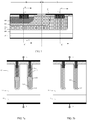
- FIG 1 is a longitudinal sectional view illustrating a semiconductor device according to the conventional technology.
- FIG 2a is a sectional view corresponding to the section along A-A' in FIG 1.
- FIG 2b is a sectional view corresponding to the section along B-B' in FIG 1 .
- the semiconductor device according to the conventional technology includes a base 110, an epitaxial layer 120, a body region 121, a source region (not shown), and a split-gate structure.
- the split-gate structure is provided with a trench.
- the split-gate structure includes a split polysilicon 132 and a gate polysilicon 135, which are formed in the trench, an oxide layer 131 formed between the split polysilicon 132 and a side wall of the trench, and a gate oxide layer 134 formed between the gate polysilicon 135 and the side wall of the trench.
- the gate polysilicon 135 is connected to a gate G
- the split polysilicon 132 is connected to a source S.
- the split-gate is located in a cell region M.
- a lead-out region of the split polysilicon 132 is a peripheral region N with respect to the cell region M.
- the split polysilicon 132 in the peripheral region N is led out to be connected to the source S.
- the conventional semiconductor device further contains the peripheral region N dedicated to lead out the split polysilicon 132, thereby increasing the area of the semiconductor device.
- the conventional technology in order to lead out the split polysilicon 132 in the peripheral region N, it is required to etch the split polysilicon 132 in the implementation process, so as to remove a portion of the split polysilicon in the cell region M and retain the split polysilicon in the peripheral region N. Therefore, it is prone to forming cavities at a side wall C of the split polysilicon 132, which affects the performance of the device.
- FIG 3 shows a semiconductor device according to an embodiment of the present disclosure.
- the semiconductor device includes: a semiconductor substrate 200 having a first conductivity type, a body region 221 formed on an upper surface layer of the substrate 200 and having a second conductivity type, and a well region 222 formed on an upper surface layer of the body region 221 and having the first conductivity type.
- the well region 222 is provided with a trench.
- the trench passes through the well region 222 and the body region 221, and extends into the substrate 200, that is, the bottom end of the trench is located in the substrate 200.
- a first polysilicon body 232 is formed at the bottom of the trench.
- a first oxide layer 231 is formed between the first polysilicon body 232 and a bottom wall of the trench and between the first polysilicon body 232 and a side wall of the trench. That is, the first oxide layer 231 is disposed between the first polysilicon body 232 and the substrate 200.
- a second polysilicon body 235 is formed on a top side wall of the trench.
- a second oxide layer 234 is formed between the second polysilicon body 235 and the side wall of the trench, and the second polysilicon body 235 does not full fill the trench.
- the second polysilicon body 235 has a hollow inner cavity.
- An isolation structure 233 is formed between the first polysilicon body 232 and the second polysilicon body 235.
- the first polysilicon body 232 and the second polysilicon body 235 are isolated from each other by the isolation structure 233.
- the trench, the polysilicon body in the trench, the isolation structure, and the oxide layer form the split-gate structure.
- An interlayer dielectric layer 240 is formed on a surface of the well region 222 and a surface of the split-gate structure, and the interlayer dielectric layer 240 is also filled into a region between the second polysilicon bodies 235 at two sides of the trench.
- a conductive plug 260 is formed in the interlayer dielectric layer 240 above the trench. The conductive plug 260 passes through the interlayer dielectric layer 240 and the isolation structure 233 and extends into the first polysilicon body 232.
- the conductive plug 260 is isolated from the second polysilicon body 235 by the interlayer dielectric layer 240, that is, the conductive plug 260 passes through the interlayer dielectric layer between the second polysilicon bodies 235 at the two sides of the trench, and extends downward into the first polysilicon body 232.
- the semiconductor device further contains a source 250, a gate (not shown in FIG 3 ), and a drain 270.
- the source 250 passes through the interlayer dielectric layer 240 and the well region 222 and extends into the body region 221.
- the conductive plug 260 is connected to the source.
- the gate passes through the interlayer dielectric layer 240 and is connected to the second polysilicon body 235.
- the drain 270 is formed on a lower surface of the substrate 200.
- the above-mentioned semiconductor device includes a split-gate structure.
- the split-gate includes a first polysilicon body and a second polysilicon body which are isolated from each other.
- the first polysilicon body is connected to the gate.
- an inversion layer is formed in the body regions at two sides of the trench through the second polysilicon body and the second oxide layer, thereby forming a conductive channel to make the source-drain turned on.
- the first polysilicon body is connected to the source, which can reduce the capacitance of the gate-drain.
- the conductive plug is formed inside the trench. One end of the conductive plug is connected to the source.
- the other end of the conductive plug sequentially passes through the interlayer dielectric layer and the isolation structure, and is inserted into the first polysilicon body, that is, an electrode of the first polysilicon is led out through the conductive plug, so that the first polysilicon is connected to the source, thereby achieving a shielding effect of the first polysilicon body on the gate-drain parasitic capacitance.
- the electrode of the first polysilicon body is led out through the conductive plug in the trench, it is not required to etch the first polysilicon body to form a side wall, which can avoid the cavities formed in the side wall of the first polysilicon body due to the lithography.
- the electrode of the first polysilicon is directly led out in the split-gate cell, which can reduce the area of the device.
- the second polysilicon body 235 is isolated from the first polysilicon body 232. At least a portion of the second polysilicon body 235 is located directly above the first polysilicon body 232 to cover a portion of the top surface of the first polysilicon body 232. That is, the second polysilicon body 235 and the first polysilicon body 232 have an overlapping portion in the width direction of the trench, so that the first polysilicon body 232 can have a better shielding effect on the gate-drain capacitance.
- the first conductivity type can be N-type
- the second conductivity type can be P-type
- the second conductivity type can be P-type
- the first conductivity type can be N-type
- the semiconductor substrate 200 includes a semiconductor base 210 and an epitaxial layer 220 formed by epitaxial growth from the semiconductor base.
- the body region 221 is specifically formed on an upper surface layer of the epitaxial layer 220.
- the trench passes through the well region 222 and the body region 221 and extends into the substrate 200. Specifically, the trench passes though the well region 222 and the body region 221 and extends into the epitaxial layer 220, namely, the bottom end of the trench is located in the epitaxial layer 220.
- the source 250 includes a source lead-out structure 251 and a source metal layer 252.
- the source metal layer 252 covers the interlayer dielectric layer 240.
- One end of the source lead-out structure 251 passes through the interlayer dielectric layer 240 and the well region 222, and is inserted into the body region 221. The other end thereof is connected to the source metal layer 252.
- One end of the conductive plug 260 is inserted into the first polysilicon body 232, and the other end thereof is also connected to the source metal layer 252.
- the first oxide layer 231 is a first silicon oxide layer
- the second oxide layer 234 is a second silicon oxide layer.
- the isolation structure 233 is a third oxide layer, and the third oxide layer can be a third silicon oxide layer.
- the interlayer dielectric layer 240 is a fourth oxide layer, and the fourth oxide layer can be a fourth silicon oxide layer.
- a heavily doped region 223 is formed in the body region 221.
- the heavily doped region 223 has the second conductivity type.
- the doping concentration of the heavily doped region 223 is higher than the doping concentration of the body region 221.
- the source 250 extends into the heavily doped region 223.
- one end of the source lead-out structure 251 can extend into the heavily doped region 223, that is, the one end of the source lead-out structure 251 is surrounded by the heavily doped region 223, and the other end is connected to the source metal layer 252.
- the heavily doped region having a comparably high concentration is connected with the source lead-out structure, so that the source and the body region form a better ohmic contact, thereby reducing the on-state resistance.
- FIG 4 is a sectional view of the semiconductor device according to an embodiment taken along lateral section C-C' in FIG 3 .
- the trench includes a first trench region M located at one side and a second trench region N located at the other side.
- the first polysilicon body 232 (not shown in FIG 4 ) leads out the conductive plug 260 from the first trench region M.
- the second polysilicon body 235 leads out the gate 280 from the second trench region N, that is, the gate 280 and the conductive plug 260 are spaced from each other in the trench.
- the source 250 is led out from the body region 222, and the source 250 is located at a side of the conductive plug 260. Referring to FIGS.
- FIG 5a is a sectional view of the semiconductor device along a longitudinal section D-D' in FIG 4 , that is, FIG 5a shows a structure of the semiconductor device corresponding to the source and the lead-out region of the conductive plug.
- FIG 5b is a sectional view of the semiconductor device along a longitudinal section E-E', that is, FIG 5b shows a structure of the semiconductor device corresponding to a gate lead-out region.
- the source 250 includes the source metal layer 252 and the source lead-out structure 251.
- the gate 280 includes a gate metal layer 282 and a gate lead-out structure 281.
- FIG 5c is a sectional view of the semiconductor device along a longitudinal section F-F' in FIG 4 .
- FIG 5c is also the sectional view of the semiconductor device along a longitudinal section F-F' in FIG 5a and the sectional view of the semiconductor device along a longitudinal section F-F' in FIG 5b .
- the gate lead-out structure and the conductive plug 260 are spaced from each other, which is also advantageous to space the source metal layer 252 from the gate metal layer 282.
- the source metal layer 252 is disposed at the same side as the source lead-out structure and the conductive plug 260, thereby facilitating the connection with the source lead-out structure and the conductive plug 260.
- the gate metal layer 282 is disposed at the same side as the gate lead-out structure, thereby facilitating the connection with the gate lead-out structure.
- the second polysilicon body 235 in the second trench region N is formed on the side wall of the trench, and does not full fill the trench in the second trench region N, that is, the second trench region N also includes the interlayer dielectric layer 240, and the interlayer dielectric layer 240 is filled into the trench.
- the second polysilicon body 235 surrounds the interlayer dielectric layer 240.
- the gate is led out from the second polysilicon bodies 235 at the two sides of the interlayer dielectric layer 240 in the second trench region N.
- a width of the trench in the first trench region M is identical to a width of the trench in the second trench region.
- the second polysilicon bodies 235 having the same thickness are formed on the side walls of the trench at the two sides of the conductive plug 260, and the gate 280 is led out from the second polysilicon bodies 235 at the two sides of the conductive plug 260.
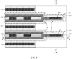
- FIG 6 is a sectional view of a semiconductor device according to another embodiment taken along the lateral section C-C' in FIG 3 .
- the width of the trench in the second trench region N is less than the width of the trench in the first trench region M.
- the second polysilicon body 235 in the second trench region N full fills the trench in the second trench region N.
- the gate 280 is led out from the second polysilicon body 235.
- the second polysilicon body 235 is to be deposited in the trench. Since the trench in the first trench region M is larger in width, the second polysilicon body 235 is formed only at the side wall of the trench in the first trench region M.
- FIG 7a is a sectional view of the semiconductor device along the section G-G' in FIG 6 .
- the corresponding region is the sectional view of the second trench region N.
- the trench above the isolation structure 233 is full filled with the second polysilicon body 235.
- FIG 7b is a sectional view of the semiconductor device taken along the section H-H' in FIG 6 .
- a depth d2 of the trench in the second trench region is less than a depth d1 of the trench in the first trench region. Since etching depth and etching width have a certain relationship during etching the trench, the smaller the etching width is, the smaller the etching depth is. In this embodiment, since the width of the trench in the second trench region N is smaller, the depth of the trench in the second trench region N is also smaller.
- the depth of the trench in the second trench region N can be adjusted according to specific situations. When the depths of the trench are different, the structures of the semiconductor device in the trench in the corresponding regions will also be different. In the present disclosure, the semiconductor devices of the first trench regions M in the trenches are substantially the same. However, the semiconductor devices of the second trench regions N can be configured differently as required. In an embodiment, as shown in FIG 8a , when the trench in the second trench region is further reduced in depth, the trench may not include the first polysilicon body. The bottom of the trench is filled with the isolation structure 233. The second polysilicon body 235 is formed on the isolation structure 233, and the second oxide layer 234 is formed between the second polysilicon body 235 and the side wall of the trench.
- the trench when the depth of the trench in the second trench region N is further reduced, the trench may not include the first polysilicon body and the isolation structure. Rather, the trench is only filled with the second polysilicon body 235, and the second oxide layer 234 is formed between the second polysilicon body 235 and the side wall of the trench.
- the present disclosure further discloses a method of manufacturing a semiconductor device.
- the manufacturing method includes following steps.
- a semiconductor substrate is provided, and the substrate has a first conductivity type.
- a split-gate structure is formed on an upper surface layer of the substrate, specifically including:
- a trench is provided on the substrate.
- the semiconductor substrate 200 includes a semiconductor base 210 and an epitaxial layer 220 formed by epitaxial growth from the semiconductor base 210. The trench is specifically formed on the epitaxial layer, and the bottom end of the trench is located in the epitaxial layer 220.
- a first oxide layer is formed on a side wall of the trench.
- a first oxide layer 231 is formed on the side wall of the trench by a thermal oxidation process.
- the first oxide layer 231 is formed on the side wall of the trench, and the trench is not full filled with the first oxide layer 231.
- a first polysilicon body is formed at a bottom of the trench.
- the trench is first full filled with the first polysilicon body 232. Then, the first polysilicon body in the upper portion of the trench is etched off by etching-back, and the first polysilicon body 232 at the bottom of the trench is retained.
- the first oxide layer located above the first polysilicon body is etched off.
- an isolation structure is formed on the first polysilicon body and the first oxide layer.
- the isolation structure can be a third oxide layer.
- the isolation structure does not full fill the trench, and is formed by deposition.
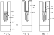
- the semiconductor device having the isolation structure is shown in FIG 10a .
- a second oxide layer is formed on a side wall of the trench above the isolation structure.
- a second oxide layer 234 is formed on a side wall of the trench by a thermal oxidation process.
- the second oxide layer 234 is formed only on the side wall of the trench, and does not full fill the trench.
- a mask layer used for etching the trench is removed prior to step S260. Therefore, during performing the thermal oxidation in step S260, a second oxide layer will also be formed on the surface of the epitaxial layer 220, and the second oxide layer 234 will not be formed on the isolation structure 233 by the thermal oxidation process.
- the second oxide layer will be formed only on the side wall of the trench and on the surface of the epitaxial layer.
- a second polysilicon body is formed on the second oxide layer, and the second polysilicon body does not full fill the trench.
- a second polysilicon body 235 is formed on the second oxide layer 234 and the isolation structure 233 in the trench by a deposition process, and the second polysilicon body 235 does not full fill the trench.
- the second polysilicon body 235 will also be formed on the second oxide layer outside the trench.
- the formed semiconductor device is shown in FIG 10b .
- the second polysilicon body is etched to remove the second polysilicon body at the bottom of the trench and retain the second polysilicon body on the side wall of the trench.
- the second polysilicon body at the bottom of the trench is etched off downwards and the second polysilicon body 235 on the side wall is retained.
- the second oxide layer and the second polysilicon body are formed on the surface of the epitaxial layer
- the second polysilicon body on the surface of the epitaxial layer is also required to be etched off, and only the second polysilicon body on the side wall of the trench is to be retained.
- the structure of the formed semiconductor device is shown in FIG 10c . At this time, the first polysilicon body 232 is isolated from the second polysilicon body 235 by the isolation structure 233 to form the split-gate structure.
- an upper surface layer of the substrate is doped to form a body region in contact with the second oxide layer, and the body region has a second conductivity type.
- the substrate 200 includes a base 210 and an epitaxial layer 220.
- the epitaxial layer 220 is doped to form a body region 221 in contact with the second oxide layer 234 on the side wall of the trench, that is, the body region 221 is located on an upper surface layer of the epitaxial layer 220.
- the second oxide layer 234 is retained on the upper surface of the epitaxial layer, the second oxide layer is patterned, and the epitaxial layer 220 is doped using the second oxide layer on the upper surface as a mask layer to form the body region 221.
- the body region is doped to form a well region in contact with the second oxide layer, and the well region has a first conductivity type.
- the body region 221 is doped to form a well region 222 in contact with the second oxide layer 234 at the side wall of the trench.
- an interlayer dielectric layer is formed on a surface of the well region and a surface of the split-gate structure, and the interlayer dielectric layer is filled into the trench.
- an interlayer dielectric layer 240 is formed on a surface of the well region 222 and a surface of the split-gate structure, and the interlayer dielectric layer 240 is filled into the trench, that is, the interlayer dielectric layer is deposited on the surface of the semiconductor device.
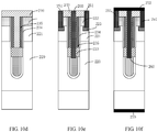
- the structure of the formed semiconductor device is shown in FIG 10d .
- a conductive plug is formed.
- the conductive plug passes through the interlayer dielectric layer and the isolation structure in the trench, and extends into the first polysilicon body.
- the conductive plug and the second polysilicon body are isolated from each other by the interlayer dielectric layer.
- a deep-trench etching is sequentially performed on the interlayer dielectric layer 240 and the isolation structure 233 in the trench, and a portion of the first polysilicon body 232 is etched, that is, a trench is formed in the split-gate structure, and a conductive material is introduced therein to form a conductive plug 260.
- the conductive plug 260 and the second polysilicon body 235 are isolated from each other by the interlayer dielectric layer 240.
- the formed semiconductor device is shown in FIG 10e .
- a source, a gate, and a drain are led out.
- the source passes through the well region and extends to the body region, and the source is connected to the conductive plug.
- the gate passes through the interlayer dielectric layer and is connected to the second polysilicon body.
- the drain is formed on a lower surface of the substrate.
- the source includes a source lead-out structure 251 and a source metal layer 252.
- the gate includes a gate lead-out structure and a gate metal layer.
- the source lead-out structure 251 and the gate lead-out structure can be formed at step S600.
- One end of the source metal lead-out structure 251 passes through the well region and is in contact with the body region 221, and the other end thereof is connected to the source metal layer 252, thereby leading out the source.
- the conductive plug 260 is connected to the source metal layer 252.
- the body region 221 is further doped to form a heavily doped region 223 having a higher concentration.
- the source 250 is connected to the structure of the heavily doped region 223.
- the formed semiconductor device is shown in FIG 10f .
- FIG 4 is a sectional view of the semiconductor device according to an embodiment taken along the lateral section C-C' in FIG 3 .
- the trench includes a first trench region M located at one side and a second trench region N located at the other side.
- the first polysilicon body 232 (not shown in FIG 4 ) leads out the conductive plug 260 from the first trench region M.
- the second polysilicon body 235 leads out the gate 280 from the second trench region N, that is, the gate 280 and the conductive plug 260 are spaced from each other in the trench.
- the source 250 is led out from the body region 222 having the second conductivity type, and the source 250 is located at one side of the conductive plug 260.
- the etching depth and the etching width have a certain relationship during etching the trench, the smaller the etching width is, the smaller the etching depth is.
- the depth of the trench can be adjusted by changing the width of the trench, so that the depth of the trench in the second trench region N is smaller than the depth of the trench in the first trench region M.
- the trench may not include the first polysilicon body.
- the bottom of the trench is filled with the isolation structure 233.
- the second polysilicon body 235 is formed on the isolation structure 233, and the second oxide layer 234 is formed between the second polysilicon body 235 and the side wall of the trench.
- the trench when the depth of the trench in the second trench region N is further reduced, the trench may not include the first polysilicon body and the isolation structure. Rather, the trench is only filled with the second polysilicon body 235, and the second oxide layer 234 is formed between the second polysilicon body 235 and the side wall of the trench.
Landscapes
- Electrodes Of Semiconductors (AREA)
- Insulated Gate Type Field-Effect Transistor (AREA)
Abstract
Description
- This application claims the benefits of the priority of
Chinese patent application No. 201811378845.9 - The present disclosure relates to the field of semiconductor technology, and particularly to a semiconductor device and a method of manufacturing a semiconductor device.
- Trench vertical double diffusion metal oxide semiconductor (VDMOS) field effect transistors adopt generally a split-gate structure in order to decrease the gate-drain parasitic capacitance. The split-gate structure contains gate polysilicon and split polysilicon, which are isolated from each other, wherein the split polysilicon proximate to the drain is connected to the source, and the gate polysilicon located on the split polysilicon is connected to the gate. To achieve the connection of the split polysilicon and the source, the split polysilicon is generally led out from the peripheral region of the cell in which the split-gate is located, so that the split polysilicon is connected to the source in the peripheral region of the split-gate. However, on the one hand, in order to lead the split polysilicon out of the split-gate cell, it is required to etch the split polysilicon in the manufacturing process, thereby resulting in cavities caused by etching on the surface of the split polysilicon. On the other hand, leading out the split polysilicon out of the split-gate region can also result in the increase of the area of the device.
- According to various embodiments of the present disclosure, a semiconductor device and a method of manufacturing the semiconductor device are provided.
- A semiconductor device is provided, including:
- a semiconductor substrate having a first conductivity type;
- a body region having a second conductivity type and formed on an upper surface layer of the substrate;
- a well region having the first conductivity type and formed on a surface layer of the body region having the second conductivity;
- a split-gate structure provided with a trench passing through the well region and the body region and extending to the substrate, the split-gate structure including:
- a first polysilicon body formed at a bottom of the trench, and a first oxide layer being formed between the first polysilicon body, and a bottom wall and a side wall of the trench;
- a second polysilicon body formed on a top side wall of the trench and not full filling the trench, and a second oxide layer being formed between the second polysilicon body and the side wall of the trench; and
- an isolation structure formed between the first polysilicon body and the second polysilicon body to isolate the first polysilicon body from the second polysilicon body;
- an interlayer dielectric layer formed on a surface of the well region and a surface of the split-gate structure and filled into the trench;
- a source passing through the interlayer dielectric layer and the well region and extending to the body region;
- a conductive plug passing through the interlayer dielectric layer and the isolation structure in the trench and extending into the first polysilicon body, the conductive plug being connected to the source, the second polysilicon body and the conductive plug being isolated from each other by the interlayer dielectric layer;
- a gate passing through the interlayer dielectric layer and connected to the second polysilicon body; and
- a drain formed on a lower surface of the substrate having the first conductivity type.
- A method of manufacturing a semiconductor device is provided, including:
- providing a semiconductor substrate, and the substrate having a first conductivity type;
- forming a split-gate structure on the substrate, including:
- providing a trench on the substrate;
- forming a first oxide layer on a side wall of the trench;
- forming a first polysilicon body at a bottom of the trench;
- etching off the first oxide layer located above the first polysilicon body;
- forming an isolation structure on the first polysilicon body and the first oxide layer;
- forming a second oxide layer on the side wall of the trench located above the isolation structure;
- forming a second polysilicon body on the second oxide layer and the isolation structure, the second polysilicon body not full filling the trench; and
- etching the second polysilicon body to remove the second polysilicon body at the bottom of the trench and retain the second polysilicon body on the side wall of the trench;
- doping an upper surface layer of the substrate to form a body region in contact with the second oxide layer, and the body region having a second conductivity type;
- doping the body region to form a well region in contact with the second oxide layer, the well region having a first conductivity type;
- forming an interlayer dielectric layer on a surface of the well region and a surface of the split-gate structure, the interlayer dielectric layer being filled into the trench;
- forming a conductive plug, the conductive plug passing through the interlayer dielectric layer and the isolation structure in the trench, and extending into the first polysilicon body, the conductive plug and the second polysilicon body being isolated from each other by the interlayer dielectric layer; and
- leading out a source, a gate, and a drain, the source passing through the well region and extending to the body region, the source being connected to the conductive plug, the gate passing through the interlayer dielectric layer and being connected to the second polysilicon body, the drain being formed on a lower surface of the substrate.
- One or more embodiments of the present disclosure will be described in detail in the following figures and description. Other features, objects and advantages of this application will become more apparent from the description, drawings and claims.
- In order to better describe and illustrate the embodiments and/or examples of the inventions disclosed herein, one or more figures can be referred to. The additional details or examples for illustrating the drawings should not be deemed as limiting the scope of any one of the disclosed inventions, the currently described embodiments and/or examples, and the best mode of the inventions currently understood.
-
FIG 1 is a sectional view of a semiconductor device in the conventional technology; -
FIG 2a is a sectional view of the semiconductor device ofFIG 1 taken along A-A' section; -
FIG 2b is a sectional view of the semiconductor device ofFIG 1 taken along B-B' section; -
FIG 3 is a schematic view of a semiconductor device according to an embodiment of the present disclosure; -
FIG 4 is a sectional view of a semiconductor device according to an embodiment taken along C-C' section inFIG 3 ; -
FIG 5a is a sectional view of the semiconductor device according to an embodiment taken along D-D' section inFIG 4 ; -
FIG 5b is a sectional view of the semiconductor device according to an embodiment taken along E-E' section inFIG 4 ; -
FIG 5c is a sectional view of the semiconductor device according to an embodiment taken along F-F' section inFIG 4 ; -
FIG 6 is a sectional view of a semiconductor device according to another embodiment taken along C-C' section inFIG 3 ; -
FIG 7a is a sectional view of the semiconductor device according to an embodiment taken along G-G' section inFIG 6 ; -
FIG 7b is a sectional view of the semiconductor device according to an embodiment taken along H-H' section inFIG 6 ; -
FIG 8a shows a trench structure in a gate lead-out region according to an embodiment; -
FIG 8b shows a trench structure in a gate lead-out region according to another embodiment; -
FIG 9 is a flow chart of a method of manufacturing a semiconductor device according to an embodiment; and -
FIGS. 10a to 10f are device structure diagrams corresponding to the related steps of a method of manufacturing a semiconductor according to an embodiment. -
FIG 1 is a longitudinal sectional view illustrating a semiconductor device according to the conventional technology.FIG 2a is a sectional view corresponding to the section along A-A' inFIG 1. FIG 2b is a sectional view corresponding to the section along B-B' inFIG 1 . The semiconductor device according to the conventional technology includes abase 110, anepitaxial layer 120, abody region 121, a source region (not shown), and a split-gate structure. The split-gate structure is provided with a trench. The split-gate structure includes asplit polysilicon 132 and agate polysilicon 135, which are formed in the trench, anoxide layer 131 formed between thesplit polysilicon 132 and a side wall of the trench, and agate oxide layer 134 formed between thegate polysilicon 135 and the side wall of the trench. Thegate polysilicon 135 is connected to a gate G Thesplit polysilicon 132 is connected to a source S. In the semiconductor device according to the conventional technology, the split-gate is located in a cell region M. A lead-out region of thesplit polysilicon 132 is a peripheral region N with respect to the cell region M. The splitpolysilicon 132 in the peripheral region N is led out to be connected to the source S. That is, the conventional semiconductor device further contains the peripheral region N dedicated to lead out thesplit polysilicon 132, thereby increasing the area of the semiconductor device. Moreover, in the conventional technology, in order to lead out thesplit polysilicon 132 in the peripheral region N, it is required to etch thesplit polysilicon 132 in the implementation process, so as to remove a portion of the split polysilicon in the cell region M and retain the split polysilicon in the peripheral region N. Therefore, it is prone to forming cavities at a side wall C of thesplit polysilicon 132, which affects the performance of the device. -
FIG 3 shows a semiconductor device according to an embodiment of the present disclosure. The semiconductor device includes: asemiconductor substrate 200 having a first conductivity type, abody region 221 formed on an upper surface layer of thesubstrate 200 and having a second conductivity type, and awell region 222 formed on an upper surface layer of thebody region 221 and having the first conductivity type. - The
well region 222 is provided with a trench. The trench passes through thewell region 222 and thebody region 221, and extends into thesubstrate 200, that is, the bottom end of the trench is located in thesubstrate 200. Afirst polysilicon body 232 is formed at the bottom of the trench. Afirst oxide layer 231 is formed between thefirst polysilicon body 232 and a bottom wall of the trench and between thefirst polysilicon body 232 and a side wall of the trench. That is, thefirst oxide layer 231 is disposed between thefirst polysilicon body 232 and thesubstrate 200. Asecond polysilicon body 235 is formed on a top side wall of the trench. Asecond oxide layer 234 is formed between thesecond polysilicon body 235 and the side wall of the trench, and thesecond polysilicon body 235 does not full fill the trench. Thesecond polysilicon body 235 has a hollow inner cavity. Anisolation structure 233 is formed between thefirst polysilicon body 232 and thesecond polysilicon body 235. Thefirst polysilicon body 232 and thesecond polysilicon body 235 are isolated from each other by theisolation structure 233. The trench, the polysilicon body in the trench, the isolation structure, and the oxide layer form the split-gate structure. Moreover, by providing theisolation structure 233, it is advantageous to flexibly adjust the distance between thefirst polysilicon body 232 and thesecond polysilicon body 235. Aninterlayer dielectric layer 240 is formed on a surface of thewell region 222 and a surface of the split-gate structure, and theinterlayer dielectric layer 240 is also filled into a region between thesecond polysilicon bodies 235 at two sides of the trench. Aconductive plug 260 is formed in theinterlayer dielectric layer 240 above the trench. Theconductive plug 260 passes through theinterlayer dielectric layer 240 and theisolation structure 233 and extends into thefirst polysilicon body 232. Theconductive plug 260 is isolated from thesecond polysilicon body 235 by theinterlayer dielectric layer 240, that is, theconductive plug 260 passes through the interlayer dielectric layer between thesecond polysilicon bodies 235 at the two sides of the trench, and extends downward into thefirst polysilicon body 232. - The semiconductor device further contains a
source 250, a gate (not shown inFIG 3 ), and adrain 270. Thesource 250 passes through theinterlayer dielectric layer 240 and thewell region 222 and extends into thebody region 221. Theconductive plug 260 is connected to the source. The gate passes through theinterlayer dielectric layer 240 and is connected to thesecond polysilicon body 235. Thedrain 270 is formed on a lower surface of thesubstrate 200. - The above-mentioned semiconductor device includes a split-gate structure. The split-gate includes a first polysilicon body and a second polysilicon body which are isolated from each other. The first polysilicon body is connected to the gate. When a voltage is applied to the gate, an inversion layer is formed in the body regions at two sides of the trench through the second polysilicon body and the second oxide layer, thereby forming a conductive channel to make the source-drain turned on. Moreover, the first polysilicon body is connected to the source, which can reduce the capacitance of the gate-drain. In this embodiment, the conductive plug is formed inside the trench. One end of the conductive plug is connected to the source. The other end of the conductive plug sequentially passes through the interlayer dielectric layer and the isolation structure, and is inserted into the first polysilicon body, that is, an electrode of the first polysilicon is led out through the conductive plug, so that the first polysilicon is connected to the source, thereby achieving a shielding effect of the first polysilicon body on the gate-drain parasitic capacitance. In this embodiment, since the electrode of the first polysilicon body is led out through the conductive plug in the trench, it is not required to etch the first polysilicon body to form a side wall, which can avoid the cavities formed in the side wall of the first polysilicon body due to the lithography. In addition, the electrode of the first polysilicon is directly led out in the split-gate cell, which can reduce the area of the device.
- In an embodiment, the
second polysilicon body 235 is isolated from thefirst polysilicon body 232. At least a portion of thesecond polysilicon body 235 is located directly above thefirst polysilicon body 232 to cover a portion of the top surface of thefirst polysilicon body 232. That is, thesecond polysilicon body 235 and thefirst polysilicon body 232 have an overlapping portion in the width direction of the trench, so that thefirst polysilicon body 232 can have a better shielding effect on the gate-drain capacitance. - In an embodiment, the first conductivity type can be N-type, and the second conductivity type can be P-type. In another embodiment, the second conductivity type can be P-type, and the first conductivity type can be N-type.
- In an embodiment, as shown in
FIG 3 , thesemiconductor substrate 200 includes asemiconductor base 210 and anepitaxial layer 220 formed by epitaxial growth from the semiconductor base. Thebody region 221 is specifically formed on an upper surface layer of theepitaxial layer 220. The trench passes through thewell region 222 and thebody region 221 and extends into thesubstrate 200. Specifically, the trench passes though thewell region 222 and thebody region 221 and extends into theepitaxial layer 220, namely, the bottom end of the trench is located in theepitaxial layer 220. - In an embodiment, as shown in
FIG 3 , thesource 250 includes a source lead-outstructure 251 and asource metal layer 252. Thesource metal layer 252 covers theinterlayer dielectric layer 240. One end of the source lead-outstructure 251 passes through theinterlayer dielectric layer 240 and thewell region 222, and is inserted into thebody region 221. The other end thereof is connected to thesource metal layer 252. One end of theconductive plug 260 is inserted into thefirst polysilicon body 232, and the other end thereof is also connected to thesource metal layer 252. - In an embodiment, the
first oxide layer 231 is a first silicon oxide layer, and thesecond oxide layer 234 is a second silicon oxide layer. In an embodiment, theisolation structure 233 is a third oxide layer, and the third oxide layer can be a third silicon oxide layer. In an embodiment, theinterlayer dielectric layer 240 is a fourth oxide layer, and the fourth oxide layer can be a fourth silicon oxide layer. - In an embodiment, as shown in
FIG 3 , a heavily dopedregion 223 is formed in thebody region 221. The heavily dopedregion 223 has the second conductivity type. The doping concentration of the heavily dopedregion 223 is higher than the doping concentration of thebody region 221. Thesource 250 extends into the heavily dopedregion 223. Specifically, one end of the source lead-outstructure 251 can extend into the heavily dopedregion 223, that is, the one end of the source lead-outstructure 251 is surrounded by the heavily dopedregion 223, and the other end is connected to thesource metal layer 252. The heavily doped region having a comparably high concentration is connected with the source lead-out structure, so that the source and the body region form a better ohmic contact, thereby reducing the on-state resistance. -
FIG 4 is a sectional view of the semiconductor device according to an embodiment taken along lateral section C-C' inFIG 3 . The trench includes a first trench region M located at one side and a second trench region N located at the other side. The first polysilicon body 232 (not shown inFIG 4 ) leads out theconductive plug 260 from the first trench region M. Thesecond polysilicon body 235 leads out thegate 280 from the second trench region N, that is, thegate 280 and theconductive plug 260 are spaced from each other in the trench. Thesource 250 is led out from thebody region 222, and thesource 250 is located at a side of theconductive plug 260. Referring toFIGS. 5a and 5b, FIG 5a is a sectional view of the semiconductor device along a longitudinal section D-D' inFIG 4 , that is,FIG 5a shows a structure of the semiconductor device corresponding to the source and the lead-out region of the conductive plug.FIG 5b is a sectional view of the semiconductor device along a longitudinal section E-E', that is,FIG 5b shows a structure of the semiconductor device corresponding to a gate lead-out region. Thesource 250 includes thesource metal layer 252 and the source lead-outstructure 251. Thegate 280 includes agate metal layer 282 and a gate lead-outstructure 281. One end of the gate lead-outstructure 281 is connected to thegate metal layer 282, and the other end thereof passes through theinterlayer dielectric layer 240 and is connected to thesecond polysilicon body 235. In an embodiment, specifically, the source lead-outstructure 251 and theconductive plug 260 are disposed at the same side. The gate lead-outstructure 281 is disposed at the other side. The gate lead-outstructure 281 and theconductive plug 260 are spaced from each other, thereby avoiding the parasitic capacitance due to the short distance between the electrodes.FIG 5c is a sectional view of the semiconductor device along a longitudinal section F-F' inFIG 4 .FIG 5c is also the sectional view of the semiconductor device along a longitudinal section F-F' inFIG 5a and the sectional view of the semiconductor device along a longitudinal section F-F' inFIG 5b . The gate lead-out structure and theconductive plug 260 are spaced from each other, which is also advantageous to space thesource metal layer 252 from thegate metal layer 282. Thesource metal layer 252 is disposed at the same side as the source lead-out structure and theconductive plug 260, thereby facilitating the connection with the source lead-out structure and theconductive plug 260. Thegate metal layer 282 is disposed at the same side as the gate lead-out structure, thereby facilitating the connection with the gate lead-out structure. - In an embodiment, as shown in
FIG 4 , thesecond polysilicon body 235 in the second trench region N is formed on the side wall of the trench, and does not full fill the trench in the second trench region N, that is, the second trench region N also includes theinterlayer dielectric layer 240, and theinterlayer dielectric layer 240 is filled into the trench. Thesecond polysilicon body 235 surrounds theinterlayer dielectric layer 240. The gate is led out from thesecond polysilicon bodies 235 at the two sides of theinterlayer dielectric layer 240 in the second trench region N. In an embodiment, a width of the trench in the first trench region M is identical to a width of the trench in the second trench region. Thesecond polysilicon bodies 235 having the same thickness are formed on the side walls of the trench at the two sides of theconductive plug 260, and thegate 280 is led out from thesecond polysilicon bodies 235 at the two sides of theconductive plug 260. -
FIG 6 is a sectional view of a semiconductor device according to another embodiment taken along the lateral section C-C' inFIG 3 . In this embodiment, the width of the trench in the second trench region N is less than the width of the trench in the first trench region M. Thesecond polysilicon body 235 in the second trench region N full fills the trench in the second trench regionN. The gate 280 is led out from thesecond polysilicon body 235. After thesecond oxide layer 234 is formed in the trench, thesecond polysilicon body 235 is to be deposited in the trench. Since the trench in the first trench region M is larger in width, thesecond polysilicon body 235 is formed only at the side wall of the trench in the first trench region M. However, thesecond polysilicon body 235 does not full fill the trench in the first trench region M. In the second trench region N, since the width of the trench in the second trench region N is smaller, the trench in this region is full filled with thesecond polysilicon body 235.FIG 7a is a sectional view of the semiconductor device along the section G-G' inFIG 6 . The corresponding region is the sectional view of the second trench region N. The trench above theisolation structure 233 is full filled with thesecond polysilicon body 235. -
FIG 7b is a sectional view of the semiconductor device taken along the section H-H' inFIG 6 . A depth d2 of the trench in the second trench region is less than a depth d1 of the trench in the first trench region. Since etching depth and etching width have a certain relationship during etching the trench, the smaller the etching width is, the smaller the etching depth is. In this embodiment, since the width of the trench in the second trench region N is smaller, the depth of the trench in the second trench region N is also smaller. - In an embodiment, the depth of the trench in the second trench region N can be adjusted according to specific situations. When the depths of the trench are different, the structures of the semiconductor device in the trench in the corresponding regions will also be different. In the present disclosure, the semiconductor devices of the first trench regions M in the trenches are substantially the same. However, the semiconductor devices of the second trench regions N can be configured differently as required. In an embodiment, as shown in
FIG 8a , when the trench in the second trench region is further reduced in depth, the trench may not include the first polysilicon body. The bottom of the trench is filled with theisolation structure 233. Thesecond polysilicon body 235 is formed on theisolation structure 233, and thesecond oxide layer 234 is formed between thesecond polysilicon body 235 and the side wall of the trench. - In yet another embodiment, as shown in
FIG 8b , when the depth of the trench in the second trench region N is further reduced, the trench may not include the first polysilicon body and the isolation structure. Rather, the trench is only filled with thesecond polysilicon body 235, and thesecond oxide layer 234 is formed between thesecond polysilicon body 235 and the side wall of the trench. - The present disclosure further discloses a method of manufacturing a semiconductor device. In an embodiment, as shown in
FIG 9 , the manufacturing method includes following steps. - At step S100, a semiconductor substrate is provided, and the substrate has a first conductivity type.
- At step S200, a split-gate structure is formed on an upper surface layer of the substrate, specifically including:
At step S210, a trench is provided on the substrate. - In an embodiment, after a patterned mask layer is formed on the
semiconductor substrate 200, a deep reactive-ion etching is performed on the substrate to etch the trench on the substrate. In an embodiment, the mask layer can be a silicon nitride layer and a silicon oxide layer. In an embodiment, thesemiconductor substrate 200 includes asemiconductor base 210 and anepitaxial layer 220 formed by epitaxial growth from thesemiconductor base 210. The trench is specifically formed on the epitaxial layer, and the bottom end of the trench is located in theepitaxial layer 220. - At step S220, a first oxide layer is formed on a side wall of the trench.
- In an embodiment, a
first oxide layer 231 is formed on the side wall of the trench by a thermal oxidation process. Thefirst oxide layer 231 is formed on the side wall of the trench, and the trench is not full filled with thefirst oxide layer 231. - At step S230, a first polysilicon body is formed at a bottom of the trench.
- In an embodiment, the trench is first full filled with the
first polysilicon body 232. Then, the first polysilicon body in the upper portion of the trench is etched off by etching-back, and thefirst polysilicon body 232 at the bottom of the trench is retained. - At step S240, the first oxide layer located above the first polysilicon body is etched off.
- At step S250, an isolation structure is formed on the first polysilicon body and the first oxide layer.
- In an embodiment, the isolation structure can be a third oxide layer. The isolation structure does not full fill the trench, and is formed by deposition. The semiconductor device having the isolation structure is shown in
FIG 10a . - At step S260, a second oxide layer is formed on a side wall of the trench above the isolation structure.
- In an embodiment, a
second oxide layer 234 is formed on a side wall of the trench by a thermal oxidation process. Thesecond oxide layer 234 is formed only on the side wall of the trench, and does not full fill the trench. In an embodiment, a mask layer used for etching the trench is removed prior to step S260. Therefore, during performing the thermal oxidation in step S260, a second oxide layer will also be formed on the surface of theepitaxial layer 220, and thesecond oxide layer 234 will not be formed on theisolation structure 233 by the thermal oxidation process. The second oxide layer will be formed only on the side wall of the trench and on the surface of the epitaxial layer. - At step S270, a second polysilicon body is formed on the second oxide layer, and the second polysilicon body does not full fill the trench.
- In an embodiment, a
second polysilicon body 235 is formed on thesecond oxide layer 234 and theisolation structure 233 in the trench by a deposition process, and thesecond polysilicon body 235 does not full fill the trench. Thesecond polysilicon body 235 will also be formed on the second oxide layer outside the trench. The formed semiconductor device is shown inFIG 10b . - At step S280, the second polysilicon body is etched to remove the second polysilicon body at the bottom of the trench and retain the second polysilicon body on the side wall of the trench.
- In an embodiment, by an anisotropic etching, the second polysilicon body at the bottom of the trench is etched off downwards and the
second polysilicon body 235 on the side wall is retained. In an embodiment, when the second oxide layer and the second polysilicon body are formed on the surface of the epitaxial layer, the second polysilicon body on the surface of the epitaxial layer is also required to be etched off, and only the second polysilicon body on the side wall of the trench is to be retained. The structure of the formed semiconductor device is shown inFIG 10c . At this time, thefirst polysilicon body 232 is isolated from thesecond polysilicon body 235 by theisolation structure 233 to form the split-gate structure. - At step S300, an upper surface layer of the substrate is doped to form a body region in contact with the second oxide layer, and the body region has a second conductivity type.
- In an embodiment, the
substrate 200 includes abase 210 and anepitaxial layer 220. Theepitaxial layer 220 is doped to form abody region 221 in contact with thesecond oxide layer 234 on the side wall of the trench, that is, thebody region 221 is located on an upper surface layer of theepitaxial layer 220. In an embodiment, when thesecond oxide layer 234 is retained on the upper surface of the epitaxial layer, the second oxide layer is patterned, and theepitaxial layer 220 is doped using the second oxide layer on the upper surface as a mask layer to form thebody region 221. - At step S400, the body region is doped to form a well region in contact with the second oxide layer, and the well region has a first conductivity type.
- In an embodiment, the
body region 221 is doped to form awell region 222 in contact with thesecond oxide layer 234 at the side wall of the trench. - At step S500, an interlayer dielectric layer is formed on a surface of the well region and a surface of the split-gate structure, and the interlayer dielectric layer is filled into the trench.
- In an embodiment, an
interlayer dielectric layer 240 is formed on a surface of thewell region 222 and a surface of the split-gate structure, and theinterlayer dielectric layer 240 is filled into the trench, that is, the interlayer dielectric layer is deposited on the surface of the semiconductor device. The structure of the formed semiconductor device is shown inFIG 10d . - At step S600, a conductive plug is formed. The conductive plug passes through the interlayer dielectric layer and the isolation structure in the trench, and extends into the first polysilicon body. The conductive plug and the second polysilicon body are isolated from each other by the interlayer dielectric layer.
- In an embodiment, a deep-trench etching is sequentially performed on the
interlayer dielectric layer 240 and theisolation structure 233 in the trench, and a portion of thefirst polysilicon body 232 is etched, that is, a trench is formed in the split-gate structure, and a conductive material is introduced therein to form aconductive plug 260. Theconductive plug 260 and thesecond polysilicon body 235 are isolated from each other by theinterlayer dielectric layer 240. The formed semiconductor device is shown inFIG 10e . - At step S700, a source, a gate, and a drain are led out. The source passes through the well region and extends to the body region, and the source is connected to the conductive plug. The gate passes through the interlayer dielectric layer and is connected to the second polysilicon body. The drain is formed on a lower surface of the substrate.
- In an embodiment, the source includes a source lead-out
structure 251 and asource metal layer 252. The gate includes a gate lead-out structure and a gate metal layer. The source lead-outstructure 251 and the gate lead-out structure can be formed at step S600. One end of the source metal lead-outstructure 251 passes through the well region and is in contact with thebody region 221, and the other end thereof is connected to thesource metal layer 252, thereby leading out the source. Specifically, theconductive plug 260 is connected to thesource metal layer 252. - In an embodiment, at step S400, after the
body region 221 is formed, thebody region 221 is further doped to form a heavily dopedregion 223 having a higher concentration. Specifically, thesource 250 is connected to the structure of the heavily dopedregion 223. The formed semiconductor device is shown inFIG 10f . -
FIG 4 is a sectional view of the semiconductor device according to an embodiment taken along the lateral section C-C' inFIG 3 . The trench includes a first trench region M located at one side and a second trench region N located at the other side. The first polysilicon body 232 (not shown inFIG 4 ) leads out theconductive plug 260 from the first trench region M. Thesecond polysilicon body 235 leads out thegate 280 from the second trench region N, that is, thegate 280 and theconductive plug 260 are spaced from each other in the trench. Thesource 250 is led out from thebody region 222 having the second conductivity type, and thesource 250 is located at one side of theconductive plug 260. - Since the etching depth and the etching width have a certain relationship during etching the trench, the smaller the etching width is, the smaller the etching depth is. The depth of the trench can be adjusted by changing the width of the trench, so that the depth of the trench in the second trench region N is smaller than the depth of the trench in the first trench region M. In an embodiment, as shown in
FIG 8a , when the trench in the second trench region N is further reduced in depth, the trench may not include the first polysilicon body. The bottom of the trench is filled with theisolation structure 233. Thesecond polysilicon body 235 is formed on theisolation structure 233, and thesecond oxide layer 234 is formed between thesecond polysilicon body 235 and the side wall of the trench. In yet another embodiment, as shown inFIG 8b , when the depth of the trench in the second trench region N is further reduced, the trench may not include the first polysilicon body and the isolation structure. Rather, the trench is only filled with thesecond polysilicon body 235, and thesecond oxide layer 234 is formed between thesecond polysilicon body 235 and the side wall of the trench. - All technical features of the above-mentioned embodiments can be combined arbitrarily. In order to make the description concise, all possible combinations of the technical features in the above-mentioned embodiments are not exhaustively described. However, as long as there is no contradiction in the combination of these technical features, these combinations should be considered within the scope of this description.
- The above-mentioned embodiments only express a few implementations of the present disclosure, and the description is comparably specific and detailed, but it should not be interpreted as a limitation on the scope of the present disclosure. It should be pointed out that for those of ordinary skill in the art, without departing from the concept of the present disclosure, several modifications and improvements can be made, and these all fall within the protection scope of the present disclosure. Therefore, the protection scope of the disclosure should be subject to the appended claims.
Claims (15)
- A semiconductor device, comprising:a semiconductor substrate having a first conductivity type;a body region having a second conductivity type and formed on an upper surface layer of the substrate;a well region having the first conductivity type and formed on a surface layer of the body region;a split-gate structure provided with a trench passing through the well region and the body region and extending to the substrate, the split-gate structure comprising:a first polysilicon body formed at a bottom of the trench, and a first oxide layer being formed between the first polysilicon body, and a bottom wall and a side wall of the trench;a second polysilicon body formed on a top side wall of the trench and not full filling the trench, and a second oxide layer being formed between the second polysilicon body and the side wall of the trench; andan isolation structure formed between the first polysilicon body and the second polysilicon body to isolate the first polysilicon body from the secondpolysilicon body;an interlayer dielectric layer formed on a surface of the well region and a surface of the split-gate structure and filled in the trench;a source passing through the interlayer dielectric layer and the well region and extending to the body region;a conductive plug passing through the interlayer dielectric layer and the isolation structure in the trench and extending into the first polysilicon body, the conductive plug being connected to the source, the second polysilicon body and the conductive plug being isolated from each other by the interlayer dielectric layer;a gate passing through the interlayer dielectric layer and connected to the second polysilicon body; anda drain formed on a lower surface of the substrate.
- The semiconductor device of claim 1, wherein at least a portion of the second polysilicon body is located directly above the first polysilicon body to cover a portion of a top surface of the first polysilicon body.
- The semiconductor device of claim 1, wherein a heavily doped region is formed in the body region, a doping concentration of the heavily doped region is higher than a doping concentration of the body region, and the source extends into the heavily doped region.
- The semiconductor device of claim 1, wherein the trench comprises a first trench region located at one side and a second trench region located at the other side, the first polysilicon body leads out the conductive plug from the first trench region, and the second polysilicon body leads out the gate from the second trench region.
- The semiconductor device of claim 4, wherein the body region leads out the source, and the source is located at one side of the conductive plug.
- The semiconductor device of claim 5, wherein the source comprises a source lead-out structure and a source metal layer, the source lead-out structure and the conductive plug are located at the same side of the trench, one end of the source lead-out structure extends into the body region, and the other end thereof is connected to the source metal layer.
- The semiconductor device of claim 4, wherein the second polysilicon body in the second trench region is formed on the side wall of the trench and does not full fill the trench in the second trench region, the interlayer dielectric layer is filled in the trench, the second polysilicon bodies located at two sides of the interlayer dielectric layer in the second trench region lead out the gate.
- The semiconductor device of claim 4, wherein a width of the trench in the second trench region is less than a width of the trench in the first trench region, the second polysilicon body in the second trench region full fills the trench in the second trench region, and the second polysilicon body leads out the gate.
- The semiconductor device of claim 4, wherein a depth of the trench in the second trench region is less than a depth of the trench in the first trench region.
- The semiconductor device of claim 9, wherein the second trench region does not comprise the first polysilicon body, the second trench region comprises the isolation structure located at the bottom of the trench and the second polysilicon body formed on the isolation structure, and the second oxide layer is formed between the second polysilicon body and the side wall of the trench.
- The semiconductor device of claim 9, wherein the second trench region does not comprise the first polysilicon body and the isolation structure, the second trench region is filled with the second polysilicon body, the second oxide layer is formed between the second polysilicon body and the side wall of the trench.
- The semiconductor device of claim 1, wherein the isolation structure, the first oxide layer, the second oxide layer, and the interlayer dielectric layer are silicon oxide.
- A method of manufacturing a semiconductor device, comprising:providing a semiconductor substrate, and the substrate having a first conductivity type;forming a split-gate structure on the substrate, comprising:providing a trench on the substrate;forming a first oxide layer on a side wall of the trench;forming a first polysilicon body at a bottom of the trench;etching off the first oxide layer located above the first polysilicon body;forming an isolation structure on the first polysilicon body and the first oxide layer;forming a second oxide layer on a side wall of the trench located above the isolation structure;forming a second polysilicon body on the second oxide layer and the isolation structure, the second polysilicon body not full filling the trench; andetching the second polysilicon body to remove the second polysilicon body at the bottom of the trench and retain the second polysilicon body on the side wall ofthe trench;doping an upper surface layer of the substrate to form a body region in contact with the second oxide layer, and the body region having a second conductivity type;doping the body region to form a well region in contact with the second oxide layer, the well region having a first conductivity type;forming an interlayer dielectric layer on a surface of the well region and a surface of the split-gate structure, the interlayer dielectric layer being filled into the trench;forming a conductive plug, the conductive plug passing through the interlayer dielectric layer and the isolation structure in the trench, and extending into the first polysilicon body, the conductive plug and the second polysilicon body being isolated from each other by the interlayer dielectric layer; andleading out a source, a gate, and a drain, the source passing through the well region and extending to the body region, the source being connected to the conductive plug, the gate passing through the interlayer dielectric layer and being connected to the second polysilicon body, the drain being formed on a lower surface of the substrate.
- The method of manufacturing the semiconductor device of claim 13, wherein the trench comprises a first trench region located at one side and a second trench region located at the other side, the first polysilicon body leads out the conductive plug from the first trench region, the second polysilicon body leads out the gate from the second trench region, the body region having the second conductivity type leads out the source and the source is located at one side of the conductive plug.
- The method of manufacturing the semiconductor device of claim 14, wherein a depth of the trench is adjusted by controlling a width of the trench, so that a depth of the trench in the second trench region is less than a depth of the trench in the first trench region.
Applications Claiming Priority (2)
| Application Number | Priority Date | Filing Date | Title |
|---|---|---|---|
| CN201811378845.9A CN111200018B (en) | 2018-11-19 | 2018-11-19 | Semiconductor device and semiconductor device manufacturing method |
| PCT/CN2019/114244 WO2020103655A1 (en) | 2018-11-19 | 2019-10-30 | Semiconductor device and method for manufacturing semiconductor device |
Publications (2)
| Publication Number | Publication Date |
|---|---|
| EP3886178A1 true EP3886178A1 (en) | 2021-09-29 |
| EP3886178A4 EP3886178A4 (en) | 2022-08-24 |
Family
ID=70746466
Family Applications (1)
| Application Number | Title | Priority Date | Filing Date |
|---|---|---|---|
| EP19888173.2A Pending EP3886178A4 (en) | 2018-11-19 | 2019-10-30 | SEMICONDUCTOR DEVICE AND METHOD FOR MANUFACTURING THE SEMICONDUCTOR DEVICE |
Country Status (4)
| Country | Link |
|---|---|
| US (1) | US12328899B2 (en) |
| EP (1) | EP3886178A4 (en) |
| CN (1) | CN111200018B (en) |
| WO (1) | WO2020103655A1 (en) |
Families Citing this family (6)
| Publication number | Priority date | Publication date | Assignee | Title |
|---|---|---|---|---|
| TWI746094B (en) * | 2020-07-29 | 2021-11-11 | 新唐科技股份有限公司 | Semiconductor structure and method of forming the same |
| JP7792952B2 (en) * | 2020-08-19 | 2025-12-26 | 華為技術有限公司 | DrMOS, integrated circuit, electronic device, and manufacturing method |
| CN111969051B (en) * | 2020-08-28 | 2023-01-24 | 电子科技大学 | Separated gate VDMOS device with high reliability and manufacturing method thereof |
| CN114496987B (en) * | 2022-04-18 | 2022-08-02 | 绍兴中芯集成电路制造股份有限公司 | MOSFET power device, forming method thereof and CSP packaging module |
| CN115497828B (en) * | 2022-09-27 | 2025-08-12 | 芯迈半导体技术(杭州)股份有限公司 | Trench type field effect transistor and manufacturing method thereof |
| CN116864525A (en) * | 2023-07-17 | 2023-10-10 | 上海功成半导体科技有限公司 | Shielding grid power device and preparation method thereof |
Family Cites Families (10)
| Publication number | Priority date | Publication date | Assignee | Title |
|---|---|---|---|---|
| US8362548B2 (en) * | 2008-11-14 | 2013-01-29 | Semiconductor Components Industries, Llc | Contact structure for semiconductor device having trench shield electrode and method |
| US9252239B2 (en) * | 2014-05-31 | 2016-02-02 | Alpha And Omega Semiconductor Incorporated | Semiconductor power devices manufactured with self-aligned processes and more reliable electrical contacts |
| US8587054B2 (en) * | 2011-12-30 | 2013-11-19 | Force Mos Technology Co., Ltd. | Trench MOSFET with resurf stepped oxide and diffused drift region |
| US8697520B2 (en) * | 2012-03-02 | 2014-04-15 | Alpha & Omega Semiconductor Incorporationed | Method of forming an asymmetric poly gate for optimum termination design in trench power MOSFETS |
| US9570553B2 (en) * | 2013-08-19 | 2017-02-14 | Infineon Technologies Austria Ag | Semiconductor chip with integrated series resistances |
| US9595587B2 (en) | 2014-04-23 | 2017-03-14 | Alpha And Omega Semiconductor Incorporated | Split poly connection via through-poly-contact (TPC) in split-gate based power MOSFETs |
| CN106057674B (en) * | 2016-05-31 | 2019-04-09 | 上海华虹宏力半导体制造有限公司 | Fabrication method of shielded gate trench MOSFET |
| US10032728B2 (en) * | 2016-06-30 | 2018-07-24 | Alpha And Omega Semiconductor Incorporated | Trench MOSFET device and the preparation method thereof |
| CN106876279A (en) * | 2017-03-31 | 2017-06-20 | 上海华虹宏力半导体制造有限公司 | Shield grid groove power device and its manufacture method |
| CN107068763A (en) * | 2017-03-31 | 2017-08-18 | 上海华虹宏力半导体制造有限公司 | Shield grid groove power device and its manufacture method |
-
2018
- 2018-11-19 CN CN201811378845.9A patent/CN111200018B/en active Active
-
2019
- 2019-10-30 EP EP19888173.2A patent/EP3886178A4/en active Pending
- 2019-10-30 WO PCT/CN2019/114244 patent/WO2020103655A1/en not_active Ceased
- 2019-10-30 US US17/281,351 patent/US12328899B2/en active Active
Also Published As
| Publication number | Publication date |
|---|---|
| US20220045207A1 (en) | 2022-02-10 |
| US12328899B2 (en) | 2025-06-10 |
| WO2020103655A1 (en) | 2020-05-28 |
| CN111200018B (en) | 2021-12-21 |
| EP3886178A4 (en) | 2022-08-24 |
| CN111200018A (en) | 2020-05-26 |
Similar Documents
| Publication | Publication Date | Title |
|---|---|---|
| US12328899B2 (en) | Semiconductor device and method for manufacturing semiconductor device | |
| CN110400843B (en) | Transistor and method for manufacturing the same | |
| US9219003B2 (en) | Oxide terminated trench MOSFET with three or four masks | |
| US10615275B2 (en) | Semiconductor device and method of manufacturing semiconductor device | |
| CN110610994B (en) | Transverse double-diffusion metal oxide semiconductor field effect transistor | |
| JP4414863B2 (en) | Insulated gate semiconductor device and manufacturing method thereof | |
| KR101920717B1 (en) | Semiconductor device including dual parallel channel structure and method of fabricating the same | |
| CN101615632B (en) | Structure and method for forming shielded gate trench FET with interelectrode dielectric including nitride layer | |
| TWI487110B (en) | Semiconductor device and method of manufacturing same | |
| US20080296673A1 (en) | Double gate manufactured with locos techniques | |
| CN105870022A (en) | Manufacturing method of shielding gate groove MOSFET | |
| CN104779166B (en) | A kind of plough groove type divides grid power device and its manufacture method | |
| CN106129105B (en) | Trench gate power MOSFET and manufacturing method | |
| CN105895516A (en) | Method for manufacturing trench gate MOSFET with shielding grid | |
| CN114038914A (en) | Double-withstand-voltage semiconductor power device and preparation method thereof | |
| CN114446791B (en) | Method for manufacturing power semiconductor device with split gate structure | |
| CN113690303A (en) | Semiconductor device and method of making the same | |
| WO2021232813A1 (en) | Trench gate metal oxide semiconductor field effect transistor, and manufacturing method thereof | |
| KR100741919B1 (en) | Trench type MOS transistor including PUN junction gate electrode and manufacturing method thereof | |
| CN114388623A (en) | Power transistor and preparation method thereof | |
| WO2021232801A1 (en) | Igbt device and manufacturing method therefor | |
| CN102097434A (en) | Groove metal oxide semiconductor field effect transistor and manufacturing method thereof | |
| CN108807517A (en) | Groove grid super node device and its manufacturing method | |
| JP2011129667A (en) | Semiconductor device and method of manufacturing the same | |
| JP7102919B2 (en) | Manufacturing method of semiconductor devices |
Legal Events
| Date | Code | Title | Description |
|---|---|---|---|
| STAA | Information on the status of an ep patent application or granted ep patent |
Free format text: STATUS: THE INTERNATIONAL PUBLICATION HAS BEEN MADE |
|
| PUAI | Public reference made under article 153(3) epc to a published international application that has entered the european phase |
Free format text: ORIGINAL CODE: 0009012 |
|
| STAA | Information on the status of an ep patent application or granted ep patent |
Free format text: STATUS: REQUEST FOR EXAMINATION WAS MADE |
|
| 17P | Request for examination filed |
Effective date: 20210127 |
|
| AK | Designated contracting states |
Kind code of ref document: A1 Designated state(s): AL AT BE BG CH CY CZ DE DK EE ES FI FR GB GR HR HU IE IS IT LI LT LU LV MC MK MT NL NO PL PT RO RS SE SI SK SM TR |
|
| DAV | Request for validation of the european patent (deleted) | ||
| DAX | Request for extension of the european patent (deleted) | ||
| A4 | Supplementary search report drawn up and despatched |
Effective date: 20220721 |
|
| RIC1 | Information provided on ipc code assigned before grant |
Ipc: H01L 29/40 20060101ALI20220715BHEP Ipc: H01L 21/336 20060101ALI20220715BHEP Ipc: H01L 29/78 20060101AFI20220715BHEP |