EP3882971A1 - Substrat rf avec jonctions ayant un agencement amélioré - Google Patents
Substrat rf avec jonctions ayant un agencement amélioré Download PDFInfo
- Publication number
- EP3882971A1 EP3882971A1 EP21161953.1A EP21161953A EP3882971A1 EP 3882971 A1 EP3882971 A1 EP 3882971A1 EP 21161953 A EP21161953 A EP 21161953A EP 3882971 A1 EP3882971 A1 EP 3882971A1
- Authority
- EP
- European Patent Office
- Prior art keywords
- doped
- branch
- axis
- type
- sector
- Prior art date
- Legal status (The legal status is an assumption and is not a legal conclusion. Google has not performed a legal analysis and makes no representation as to the accuracy of the status listed.)
- Pending
Links
Images





Classifications
-
- H—ELECTRICITY
- H10—SEMICONDUCTOR DEVICES; ELECTRIC SOLID-STATE DEVICES NOT OTHERWISE PROVIDED FOR
- H10W—GENERIC PACKAGES, INTERCONNECTIONS, CONNECTORS OR OTHER CONSTRUCTIONAL DETAILS OF DEVICES COVERED BY CLASS H10
- H10W44/00—Electrical arrangements for controlling or matching impedance
- H10W44/20—Electrical arrangements for controlling or matching impedance at high-frequency [HF] or radio frequency [RF]
-
- H—ELECTRICITY
- H10—SEMICONDUCTOR DEVICES; ELECTRIC SOLID-STATE DEVICES NOT OTHERWISE PROVIDED FOR
- H10D—INORGANIC ELECTRIC SEMICONDUCTOR DEVICES
- H10D86/00—Integrated devices formed in or on insulating or conducting substrates, e.g. formed in silicon-on-insulator [SOI] substrates or on stainless steel or glass substrates
- H10D86/01—Manufacture or treatment
-
- H—ELECTRICITY
- H10—SEMICONDUCTOR DEVICES; ELECTRIC SOLID-STATE DEVICES NOT OTHERWISE PROVIDED FOR
- H10D—INORGANIC ELECTRIC SEMICONDUCTOR DEVICES
- H10D86/00—Integrated devices formed in or on insulating or conducting substrates, e.g. formed in silicon-on-insulator [SOI] substrates or on stainless steel or glass substrates
- H10D86/201—Integrated devices formed in or on insulating or conducting substrates, e.g. formed in silicon-on-insulator [SOI] substrates or on stainless steel or glass substrates the substrates comprising an insulating layer on a semiconductor body, e.g. SOI
-
- H—ELECTRICITY
- H10—SEMICONDUCTOR DEVICES; ELECTRIC SOLID-STATE DEVICES NOT OTHERWISE PROVIDED FOR
- H10P—GENERIC PROCESSES OR APPARATUS FOR THE MANUFACTURE OR TREATMENT OF DEVICES COVERED BY CLASS H10
- H10P90/00—Preparation of wafers not covered by a single main group of this subclass, e.g. wafer reinforcement
- H10P90/19—Preparing inhomogeneous wafers
- H10P90/1904—Preparing vertically inhomogeneous wafers
- H10P90/1906—Preparing SOI wafers
- H10P90/1914—Preparing SOI wafers using bonding
- H10P90/1916—Preparing SOI wafers using bonding with separation or delamination along an ion implanted layer, e.g. Smart-cut
-
- H—ELECTRICITY
- H10—SEMICONDUCTOR DEVICES; ELECTRIC SOLID-STATE DEVICES NOT OTHERWISE PROVIDED FOR
- H10W—GENERIC PACKAGES, INTERCONNECTIONS, CONNECTORS OR OTHER CONSTRUCTIONAL DETAILS OF DEVICES COVERED BY CLASS H10
- H10W10/00—Isolation regions in semiconductor bodies between components of integrated devices
- H10W10/10—Isolation regions comprising dielectric materials
- H10W10/181—Semiconductor-on-insulator [SOI] isolation regions, e.g. buried oxide regions of SOI wafers
-
- H—ELECTRICITY
- H10—SEMICONDUCTOR DEVICES; ELECTRIC SOLID-STATE DEVICES NOT OTHERWISE PROVIDED FOR
- H10W—GENERIC PACKAGES, INTERCONNECTIONS, CONNECTORS OR OTHER CONSTRUCTIONAL DETAILS OF DEVICES COVERED BY CLASS H10
- H10W70/00—Package substrates; Interposers; Redistribution layers [RDL]
- H10W70/60—Insulating or insulated package substrates; Interposers; Redistribution layers
- H10W70/67—Insulating or insulated package substrates; Interposers; Redistribution layers characterised by their insulating layers or insulating parts
- H10W70/69—Insulating materials thereof
- H10W70/698—Semiconductor materials that are electrically insulating, e.g. undoped silicon
-
- H—ELECTRICITY
- H10—SEMICONDUCTOR DEVICES; ELECTRIC SOLID-STATE DEVICES NOT OTHERWISE PROVIDED FOR
- H10D—INORGANIC ELECTRIC SEMICONDUCTOR DEVICES
- H10D1/00—Resistors, capacitors or inductors
- H10D1/20—Inductors
-
- H—ELECTRICITY
- H10—SEMICONDUCTOR DEVICES; ELECTRIC SOLID-STATE DEVICES NOT OTHERWISE PROVIDED FOR
- H10W—GENERIC PACKAGES, INTERCONNECTIONS, CONNECTORS OR OTHER CONSTRUCTIONAL DETAILS OF DEVICES COVERED BY CLASS H10
- H10W44/00—Electrical arrangements for controlling or matching impedance
- H10W44/20—Electrical arrangements for controlling or matching impedance at high-frequency [HF] or radio frequency [RF]
- H10W44/241—Electrical arrangements for controlling or matching impedance at high-frequency [HF] or radio frequency [RF] for passive devices or passive elements
-
- H—ELECTRICITY
- H10—SEMICONDUCTOR DEVICES; ELECTRIC SOLID-STATE DEVICES NOT OTHERWISE PROVIDED FOR
- H10W—GENERIC PACKAGES, INTERCONNECTIONS, CONNECTORS OR OTHER CONSTRUCTIONAL DETAILS OF DEVICES COVERED BY CLASS H10
- H10W44/00—Electrical arrangements for controlling or matching impedance
- H10W44/20—Electrical arrangements for controlling or matching impedance at high-frequency [HF] or radio frequency [RF]
- H10W44/241—Electrical arrangements for controlling or matching impedance at high-frequency [HF] or radio frequency [RF] for passive devices or passive elements
- H10W44/248—Electrical arrangements for controlling or matching impedance at high-frequency [HF] or radio frequency [RF] for passive devices or passive elements for antennas
Definitions
- the present application relates to the field of semiconductor substrates and in particular those intended for radiofrequency (RF) applications.
- RF radiofrequency
- a semiconductor-on-insulator type substrate is commonly formed of a support layer covered by, and in contact with, an insulating layer, itself covered by, and in contact with, a semiconductor surface layer generally intended for serve as an active layer, that is to say in which at least a part of electronic components such as transistors is intended to be formed.
- a known improvement of these substrates consists in forming under and against the insulating layer commonly called “BOX” a layer called “trap rich”, that is to say formed of a semiconductor material rich in crystalline defects and which allows to trap charges.
- N-type doped bands 2 and P-type doped bands 4 is produced in the support layer 6 of a semiconductor-on-insulator type substrate.
- junctions 1.1, 1.2, 1.3, 1.4, 1.5 provided to stop eddy currents moving perpendicularly to a main direction of elongation of parallel bands 2, 4 doped N and P.
- the conductor circuit capable of being at the origin of eddy currents is in the form of a simple metal line 8 parallel to the N and P doped bands.
- junctions 1.1, 1.2, 1.3, 1.4, 1.5 would not make it possible to block eddy currents in a direction parallel to that of the main elongation of the lines. It is then necessary to place the metal line 8 in a single arrangement on the support 6, that is to say perpendicular to the doped bands 2 and 4.
- the present invention provides a semiconductor-on-insulator type substrate provided with a semiconductor surface layer arranged on an insulating layer, the insulating layer being arranged on a support layer based on a semiconductor material.
- conductive said support layer being provided with a current blocking structure formed of a plurality of junctions for blocking the flow of parasitic currents in a plane parallel to a principal plane of the support layer, said structure comprising, in a sector doped according to a doping of a first type, in particular P or N, a plurality of distinct doped regions having a doping of a second type, in particular N or P, opposite to said first type, said doped regions being surrounded entirely by 'a zone of said doped and doping sector of the first type, said regions forming a given pattern comprising at least one first branch and at least one second branch forming a non-zero angle with said first branch, the given pattern and the distribution of said doped regions in said doped sector being provided so that: in a first direction parallel to the first
- Such a structure makes it possible to stop the parasitic currents in several directions while being adapted to various forms of RF components or RF circuits or conductive elements carrying an RF signal.
- the structure comprises in the first direction and / or in the second direction, and / or in the third direction: a succession of doped regions forming said same given pattern identical in terms of shape and / or dimensions.
- the distinct doped regions can be distributed periodically in said structure over one or more first row (s) parallel to a first axis, the first axis being parallel to the main plane of the substrate.
- the distinct doped regions are distributed periodically in said structure over one or more other rows arranged parallel to a second axis, the second axis being parallel to the main plane of the substrate, the second axis forming a non-zero angle with said first axis.
- the distinct doped regions are distributed periodically in said structure over one or more rows parallel to a first axis.
- the given pattern and the distribution of the doped regions are provided so that, whatever the given axis parallel to the first direction or to the second direction or to the third direction and passing between two said doped regions, this axis given crosses a succession of junctions.
- the possibilities of creating conductive paths of parasitic currents are thus optimally limited.
- the given pattern has a maximum expected dimension less and typically at least two times less, preferably at least ten times less, than a predetermined dimension equal to a maximum length of eddy current propagation in said semiconductor material of the support layer at an operating frequency of an RF circuit which is suitable for being disposed opposite the blocking structure.
- the first row or rows are formed of a succession of doped regions comprising alternately said given pattern in a first orientation and said given pattern in a second orientation distinct from the first orientation.
- the blocking structure can advantageously comprise several other rows parallel to the second axis, at least one given row among said other rows being formed by a repetition of said given pattern in the first orientation and at least one row adjacent to the given row being formed of a repetition of said given pattern in said second orientation.
- the given pattern can include a first branch and a second branch forming a non-zero angle with the first branch, in particular orthogonal to the first branch.
- said distinct doped regions are distributed periodically in said structure over one or more other rows parallel to a second axis, the first axis and said second axis being axes parallel to said main plane, said second axis forming an angle of less than 90 ° with said first axis, among said first rows at least one given row being formed of a first succession of doped regions reproducing said given pattern, at least one neighboring row of said given row being formed of a second succession of doped regions reproducing said given pattern, said neighboring row being offset from said given row with respect to to a plane orthogonal to the first axis and to said main plane.
- it may include a first branch, a second branch at a first end of the first branch and forming a non-zero angle with the first branch, and a third branch at a second end of the first branch and forming a non-zero angle with the first branch, the second branch and the third branch having respective different orientations in a plane parallel to a main plane of the support layer.
- the given pattern comprises a first main branch, a second main branch, a third main branch, a fourth main branch, said main branches meeting in an intersection region, the pattern further comprising secondary branches each connected to a main branch, the secondary branches following different respective orientations in a plane parallel to a main plane of the support layer.
- the given pattern is formed by a succession of branches of different respective orientations and forming a spiral.
- the structure comprises in the first direction, in the second direction, in the third direction: a succession of doped regions forming said same given pattern identical in terms of shape, dimensions, and orientation with respect to a direction given among said first direction, second direction, third direction.
- the RF component is an antenna and / or an inductor.
- the given pattern has a maximum dimension measured parallel to the main plane of the substrate, provided less and typically at least two times less, advantageously at least ten times less than a predetermined dimension equal to the length of eddy current propagation in said material semiconductor of the support layer at said operating frequency.
- FIG. 2A-2B An exemplary embodiment of a structure for blocking parasitic currents, in particular eddy currents, in a substrate such as implemented according to an embodiment of the present invention, will now be given in connection with the figures 2A-2B (respectively giving a cross-sectional view of the substrate with the blocking structure and a top view of this structure).
- the structure is produced in an upper part of a semiconductor support layer 10 of a substrate, for example of the semiconductor-on-insulator type.
- This structure is in the form of a doped volume 20 of the support layer 10 and is placed against, and preferably in contact with, the insulating layer 11 of the substrate.
- the insulating layer 11 is arranged on the support layer 10 and separates this support layer 10 from a surface semiconductor layer 12 in which transistor channels can be provided.
- the substrate may in particular be of the SOI (“Silicon On Insulator”, i.e. “silicon on insulator”) type, ie with a surface semiconductor layer 12 of silicon.
- SOI Silicon On Insulator
- the semiconductor surface layer 12 can be provided with a thickness between 4 nm and 50 nm.
- the insulating layer 11 is for its part typically based on silicon oxide and may have a thickness of, for example, between 15 nm and 250 nm.
- the semiconductor support layer 10 may also be made of silicon and comprise, under the doped volume 20, a layer of semiconductor material of high resistivity, for example greater than 1000. cm, and advantageously greater than 5000 cm.
- the doped volume 20 can for its part have a thickness e 1 (dimension measured parallel to the z axis of an orthogonal reference mark [0; x; y; z] indicated in the figures) comprised for example between 50 nm and 1 ⁇ m. , advantageously between 100 nm and 500 nm.
- the doped volume 20 is here formed of a sector 22 doped according to a doping of a first type, conferring a first type of conductivity, for example of P type, and of a plurality of doped regions 23. There is provided in the blocking structure a repetition of doped regions 23 distinct from one another producing the same pattern M 1 , M ′ 1 which is identical in terms of size and shape.
- the doped regions 23 have a doping of a second type, conferring a second type of conductivity opposite to the said sector.
- first type of conductivity for example of type N.
- doping of type N one understands a doping which consists in installing an excess of electrons
- doping of type P one understands a doping which consists in installing an excess of electrons. holes.
- the doped regions 23 are thus surrounded, preferably entirely surrounded, by portions of said doped sector 22 having doping of the opposite type.
- the volume 20 thus comprises junctions 25a, 25b PN or NP each formed, between on the one hand a zone of the sector 22 doped according to said doping of the first type and on the other hand one of said doped regions 23 according to the doping of the second type or Conversely.
- Such an arrangement contributes to limiting or even preventing the propagation of parasitic eddy current of the type of that referenced C 1 on the figure 5 .
- a parasitic current is in fact likely to cross contiguous doped regions along a diagonal, relative to the longitudinal and transverse rows of the checkerboard.
- the succession of doped patterns is such that the doped regions 23 are distributed periodically in the structure over at least one row 31, 32, 33. These regions 23 may themselves be arranged in several rows arranged parallel to a first one. axis ⁇ 1 , this axis ⁇ 1 being parallel to a main plane of the substrate.
- main plane of the substrate is meant here a plane passing through the substrate and which is parallel to the plane [O; x; y] given in the figures.
- a matrix arrangement of doped regions 23 distributed in rows and columns can in particular be provided.
- the doped regions 23 are also distributed in rows 31 parallel to a second axis ⁇ 2 , this second axis being in this example parallel to the main plane of the substrate and orthogonal to the first axis ⁇ 1 .
- the periodic arrangement of the regions 23 is such that in a first direction parallel to the first axis ⁇ 1 , said structure comprises one or more junctions 25a, 25b, making it possible to block parasitic currents in this first direction, while in a second orthogonal direction in the first direction and parallel to the second axis ⁇ 2 , said structure comprises one or more junctions 25a, 25b making it possible to block parasitic currents in this second direction, and that in at least a third direction parallel to a third axis ⁇ 3 and achieving a non-zero angle, for example 45 °, with said first and second directions and crossing said structure, said structure comprises one or more junctions 25a, 25b making it possible to block parasitic currents in this third direction.
- the extent (in other words the footprint or the occupied surface) of the blocking structure or of the measured doped volume is adapted ( e) in a plane parallel to the main plane of the substrate, as a function of that of the RF component, for example of antenna or inductor type, and of this operating frequency.
- the extent of the blocking structure is thus preferably greater than that of the antenna and for example, for an antenna of 30 GHz, an excess L D ⁇ Ip of at least 1 mm, representing the maximum propagation length of the currents de Foucault, is expected.
- the maximum length of the doped regions 23 in other words the maximum dimension D M of the units M 1 , M ' 1 measured. parallel to the plane [0; x; y] of the orthogonal coordinate system [0; x; y; z] as a function of the dimension Ip and preferably so that 2 ⁇ D M ⁇ Ip.
- the maximum dimension D M is much less, that is to say at least 10 times less than the dimensions of the antenna and the propagation length Ip.
- a device provided with such a blocking structure has a large number of junctions making it possible to block parasitic currents in at least 3 different directions (for example 45 ° difference).
- the N-type doped regions 23 preferably follow the same pattern M 1 , M ′ 1 .
- this pattern M 1 , M ' 1 is formed of at least a first branch b 1 and at least one second branch b 2 connected to the first branch b 1 and forming a non-zero angle with the first branch b 1 .
- This distinguishes itself from rectangular or square-shaped patterns such as, for example, those shown on the figures 6 , 7 and which, in a checkerboard matrix arrangement would promote the formation of parasitic current paths C ' 1 , C' 2 . With such a form of patterns, the possibility of creating parasitic current paths is limited.
- the first branch b 1 and / or the second branch b 2 of the pattern M 1 , M ' 1 can be provided with a critical dimension dc (dimension measured parallel to the plane [0; x; y] corresponding to the smallest dimension d' a pattern except its thickness) for example between 500 nm and 10 ⁇ m, advantageously between 1 ⁇ m and 5 ⁇ m
- a maximum dimension D M of between 5 ⁇ m and 100 ⁇ m, advantageously between 25 ⁇ m and 50 ⁇ m, while a minimum space d min between 500 nm and 10 ⁇ m, advantageously between 1 ⁇ m and 5 ⁇ m can be designed for tracks width between 500 nm and 10 ⁇ m
- the repetition and the distribution in rows of the doped regions 23 according to a pattern or according to the same determined sequence of patterns makes it possible to provide an RF component or RF conducting circuit or a conducting element facing the doped volume 20 without necessarily having to perform precise alignment of this component or of this circuit or of this conductive element with respect to the junctions and in particular to the borders of the doped regions 23.
- the blocking structure can thus be advantageously designed without necessarily knowing beforehand the exact design of the RF circuit or RF component made to be produced opposite the doped volume 20.
- the dimensions of the tracks forming the RF circuit or component as well as the overall size of this component or of the circuit can then be sufficient.
- the pattern M 1 , M ' 1 reproduced in a matrix arrangement is a pattern in the shape of a' T ', with an alternation of rows 32 in which the pattern M 1 has a first orientation with respect to the axis ⁇ 1 and of rows 33 in which the pattern M ' 1 follows a second orientation, the patterns M 1 , M' 1 of a row 32 being in this particular example of arrangement arranged head-to-tail, that is to say according to a rotation by 180 °, relative to those M ' 1 of the neighboring row 33.
- FIG 2B allows to illustrate an advantageous mode in particular compared to those illustrated on the figures 8 and 9 , where other types of 'L' shaped and simple cross, or '+', or pattern consisting of four branches are used.
- the arrangement of the patterns M 1 , M ' 1 and their shape are determined so that whatever the given axis parallel to the first axis ⁇ 1 , or to the second axis ⁇ 2 or to the third axis ⁇ 3 passing through the structure and passing through an area of the sector 22 between two neighboring doped regions 23, this given axis encounters an alternation of N-type doped areas and P-type doped area, with at least one PN junction and at least one NP junction.
- Parasitic conductive paths such as those C 3 , C 4 shown schematically on the figures 8 and 9 are thus avoided.
- a second example of the blocking structure is given on figure 3 . It differs from the example described above, in particular by the shape of the doped regions 23, as well as by their distribution in the doped sector 22.
- the doped regions 23 here have an identical pattern M 2 repeated, advantageously periodically, and preferably according to a matrix arrangement in which the repetition of patterns is carried out on several axes ⁇ 1 , ⁇ ' 2 .
- the pattern M 2 comprises, in this particular example, a first branch b 11 , a second branch b 12 located at a first end of the first branch b 11 and a third branch b 13 located at a second end of the first branch b 11 .
- the branches b 12 and b 13 form a non-zero angle, for example 90 ° with the first branch b 11 .
- the second branch b12 and the third b13 have parallel directions of elongation and in opposite respective directions.
- the pattern M 2 is, here, not U-shaped.
- Such a pattern M 2 with several branches extending in different directions (with respect to b11) participates in the implementation of a blocking of current in several directions.
- a regular arrangement of the regions 23 in lines parallel to a first axis ⁇ 1 is provided.
- a positioning offset of the patterns is implemented between successive neighboring rows 31a, 31b parallel to the first axis ⁇ 1 .
- the offset between neighboring rows is here an offset taken with respect to a plane P orthogonal to the main plane of the substrate and orthogonal to the first axis ⁇ 1 .
- a given row 31a formed of a succession of patterns M 2 is, with respect to an axis orthogonal to the first axis ⁇ 1, offset with respect to a neighboring row of said given row formed of another succession of said same given pattern M 2 .
- a distribution of the patterns M 2 in rows parallel to a second axis ⁇ ' 2 non-orthogonal to the first axis is carried out here.
- the structure for blocking parasitic currents can, as in the previous embodiment, be produced without precise knowledge of the arrangement of the tracks.
- blocking is implemented in at least 3 distinct directions, in particular at least 45 ° relative to each other.
- a third embodiment of a blocking structure is given on figure 4 . It differs from the previous example in particular by the shape of the doped regions 23.
- the doped regions 23 here have a pattern M 3 formed of four main forms b 21 , b 22 , b 23 , b 24 meeting in an intersection region and four secondary branches b 25 , b 26 , b 27 , b 28 each located at a respective end of a branch main b 21 , b 22 , b 23 , b 24 , the secondary branches b 25 , b 26 , b 27 , b 28 following different respective orientations.
- Such a pattern M 3 makes it possible to facilitate an arrangement in which branches of neighboring patterns interpenetrate to create zones of the doped sector 22 according to the doping of the first type and making a sinuous path. This helps to limit or even prevent the flow of eddy currents.
- the pattern has been represented without an angle but the person skilled in the art will be able to adapt this pattern with an angle, in particular a right angle, between a main branch and its secondary branch in order to produce this pattern with the lithography techniques currently available.
- the pattern M 3 is similar to that of a swastika but other patterns with main and secondary branches can be used.
- main branches form between them an angle other than 90 ° and / or in which the secondary branches b 25 , b 26 , b 27 , b 28 make an angle different from 90 ° with the main branches and / or in which other so-called “tertiary” branches originating from the secondary branches form a non-zero angle with its later ones.
- the regular distribution according to a predetermined pitch of the patterns M 3 makes it possible to produce a blocking structure making it possible to prevent the flow of eddy current without necessarily having to know in advance the arrangement of the conductive tracks.
- a blocking structure which comprises in the first direction, in the second direction, in the third direction: a succession of doped regions forming said same given pattern identical in terms of shape, dimensions, and possibly orientation with respect to a given direction from among said first direction, second direction, third direction is particularly advantageous. Optimal blocking is achieved while avoiding the problem of alignment with a passive component or an antenna.
- a blocking structure comprises in the first direction, in the second direction, in the third direction: a succession of doped regions forming said same given pattern identical in terms of shape, dimensions, and orientation with respect to a given direction among said first direction, second direction, third direction.
- FIG. 15 Another exemplary embodiment of a blocking structure is given on figure 15 . It differs in the shape of the doped regions 23.
- the doped regions 23 here produce a pattern M 4 in the form of a spiral composed of a succession of branches b 31 , b 32 , b 33 , b 34 ... distinct from orientations. different from each other.
- the branches here in the form of turns do not touch each other, nor from one pattern M 4 to another.
- the branches may have a critical dimension for example of the order of 100 nm, the spiral pattern having a maximum dimension for example of the order of 1.5 ⁇ m, much less than that of a passive component of inductor or antenna type.
- a conductive track 51 for example of an antenna or an inductor, through which an RF signal is intended to pass is positioned above and opposite the doped volume 20 in which the repeated succession PN and / or NP junctions is produced.
- This conductive track 51 can be positioned without necessarily being aligned with and / or without taking into account the orientation of one or the other of the branches b 21 , b 22 , b 23 , b 24 , b 25 , b 26 , b 27 , b 28 of the unit or units M 3 of the blocking structure.
- the conductive track 51 can be an inductance portion 160 forming a loop in the shape of a polygon as illustrated on the figure. figure 11A or the generally rectangular one on the figure 11B .
- knowing the area occupied by the inductor 160 and the track width 60 makes it possible to carry out the blocking structure 20 without necessarily knowing the orientation of the conductive tracks relative to the doped patterns.
- a possible starting material for this process is here a solid substrate, in other words of the type commonly called “bulk” formed from a wafer of semiconductor material.
- the solid substrate is here intended to form the support layer in which the blocking structure is made.
- a surface layer of this support layer 10 can first of all be doped, for example by implantation, to produce the doped sector 22 ( figure 12A ).
- a doping of a first type is carried out so as to form a doped sector 22.
- a sector 22 is produced having a doping of type P.
- a boron implantation according to an energy of for example between 10 keV and 150 keV, and a dose of for example between 10 14 cm -2 and 10 15 cm -2 .
- a mask 110 with implantation comprising distinct openings 111 each reproducing a given pattern, for example one of the patterns M 1 , M 2 , M 3 described above.
- the mask 110 may for example be based on a resin in which the openings 111 are made, for example by means of a photolithography process.
- the doped regions 23 are then formed according to a doping of the opposite type. For example, if one carries out an implantation using a donor species through the openings 111 of the mask 110, one can realize regions 23 having an N-type doping ( figure 12B ) in the parts exposed by the openings 111.
- N-doped regions 23 in the P-doped sector 22 it is possible, for example, to carry out a phosphorus implantation according to an energy of for example between 20 keV and 200 keV, and a dose of for example between 10 14 cm -2 and 10 15 cm -2 .
- an implantation of Arsenic at an energy of for example between 40 keV and 200 keV, and a dose of for example between 10 14 cm -2 and 10 15 cm -2 can be carried out to form the regions 23 .
- the dose used to form the doped regions 23 is preferably greater than that of the doped sector 22, in order to be able to locally invert the type of conductivity in the doped regions 23 and to be able to create P-doped regions in an overall N-doped sector or vice versa. N-doped regions in a globally P-doped sector.
- Mask 110 can then be removed.
- this mask 110 can be removed by etching using an oxygen plasma and / or a bath containing a mixture of sulfuric acid. and hydrogen peroxide.
- a “hard” mask can advantageously be used, for example of silicon oxide or nitride, previously etched by photolithography and etching, for example by plasma. The hard mask can then be removed chemically, using an HF solution for an oxide mask or H 3 PO 4 for a nitride mask.
- An insulating layer 11 can then be formed on the support layer 10, for example by depositing silicon oxide.
- a semiconductor layer 12 intended to form the surface layer of the semiconductor-on-insulator substrate is transferred.
- This surface layer can be produced, for example, by transferring a handle semiconductor support, for example made of silicon, which is bonded to the insulating layer 11 typically by performing bonding by molecular adhesion.
- An oxide layer may optionally be provided on this handle support in order to achieve bonding of the oxide-on-oxide type.
- An area of weakness is produced in the handle support, for example by implanting the handle support. Then, one can perform a separation of one thickness of the handle support at the level of the weakening zone, so as to keep another thickness of this support which then forms the semiconductor layer.
- superficial 12 ( figure 12C ).
- the surface layer 12 can be produced using a process of the type commonly called Smart cut TM.
- the semiconductor-on-insulator substrate is then ready to accommodate one or more electronic components as well as at least one RF component or RF circuit.
- the junctions can be formed directly in the support layer of a substrate of semiconductor-on-insulator type, for example using a first implantation for perform the doped sector 22 then another implantation through the openings of a mask to produce the doped regions 23.
- a subsequent step of forming conductive tracks 60 of this RF component or RF circuit by producing a first metallic level is illustrated on the figure. figure 12 .
- the RF circuit is typically produced on at least two metallization levels, with one or more conductive tracks of a first level connected to one or more conductive tracks of a second level.
- the blocking structure formed of PN or NP junctions and as implemented according to the invention can then make it possible to prevent the circulation of parasitic currents likely to be generated by a current circulation on each of the metallization levels of the RF circuit. .
- an eddy current blocking structure such as implemented according to the invention can be arranged on a substrate of the semiconductor-on-insulator type, or else on a solid substrate on which an insulating layer is. typically added.
- the doped volume 20 in which the blocking structure is produced is formed in the semiconductor support layer 100 of a substrate and facing a region R 2 over which an insulating layer 131 extends, for example d silicon oxide and of thickness which may be for example between 50 nm and 1 ⁇ m
- the RF component 160 for example in the form of an antenna, is arranged on this insulating layer 131, while another region R 1 of the support layer 100 is, for its part, not covered by the insulating layer 111.
- This other region R 2 can be dedicated to other types of components and / or circuits. For example, it is possible to provide logic components on this other region R 1 .
Landscapes
- Semiconductor Integrated Circuits (AREA)
- Metal-Oxide And Bipolar Metal-Oxide Semiconductor Integrated Circuits (AREA)
- Crystals, And After-Treatments Of Crystals (AREA)
- Element Separation (AREA)
- Insulated Gate Type Field-Effect Transistor (AREA)
Abstract
Description
- La présente demande concerne le domaine des substrats semiconducteurs et en particulier ceux destinés à des applications radiofréquences (RF).
- Un substrat de type semi-conducteur sur isolant est communément formé d'une couche de support recouverte par, et en contact avec, une couche isolante, elle-même recouverte par, et en contact avec, une couche superficielle semi-conductrice généralement destinée à servir de couche active, c'est-à-dire dans laquelle au moins une partie de composants électroniques tels que des transistors est destinée à être formée.
- Pour des applications radiofréquences des adaptations d'un tel substrat peuvent s'avérer nécessaires. Des champs parasites sont en effet susceptibles de venir perturber le fonctionnement du substrat, en particulier lorsque des fréquences élevées par exemple supérieures à 5 GHz, sont utilisées.
- Une amélioration connue de ces substrats consiste à former sous et contre la couche isolante communément appelée « BOX » une couche dite « trap rich », c'est-à-dire formée d'un matériau semi-conducteur riche en défauts cristallins et qui permet de piéger des charges.
- Avec une telle couche, on limite la conduction parasite à proximité de la couche isolante, et on améliore de cette manière les performances des circuits radiofréquences en termes d'isolation radiofréquences, de diminution des pertes d'insertion et d'intégrité du signal.
- Une autre manière de limiter la circulation des courants parasites et en particulier des courants de Foucault (en anglais « eddy currents ») sous la couche isolante et à proximité de l'interface entre cette couche isolante et la couche de support semi-conductrice est proposée dans le document "Low-Loss Si-Substrates Enhanced Using Buried PN Junctions for RF Applications" de Rack et al., IEEE Electron Device Letters, vol. 40, n°5, p. 690, 2019.
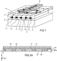
- Dans ce document, une alternance de bandes dopées 2 de type N et de bandes dopées 4 de type P est réalisée dans la couche de support 6 d'un substrat de type semi-conducteur sur isolant.
- Un tel type d'agencement, illustré sur la
figure 1 , permet de former des jonctions 1.1, 1.2, 1.3, 1.4, 1.5 prévues pour stopper des courants de Foucault se dirigeant perpendiculairement à une direction principale d'allongement des bandes parallèles 2, 4 dopées N et P. - Dans l'exemple illustré, le circuit conducteur susceptible d'être à l'origine de courants de Foucault est sous forme d'une simple ligne métallique 8 parallèle aux bandes dopées N et P.
- Mais un tel agencement des jonctions n'est pas adapté à un cas où le circuit RF prend une forme plus complexe. En effet, dans l'exemple illustré, les jonctions 1.1, 1.2, 1.3, 1.4, 1.5 ne permettraient pas de bloquer des courants de Foucault dans une direction parallèle à celle d'allongement principal des lignes. Il est alors nécessaire de placer la ligne métallique 8 selon une unique disposition sur le support 6, c'est-à-dire perpendiculairement aux bandes dopées 2 et 4.
- Il se pose le problème de réaliser une nouvelle structure qui soit améliorée vis-à-vis d'inconvénient(s) mentionné(s) ci-dessus.
- Selon un mode de réalisation, la présente invention prévoit un substrat de type semi-conducteur sur isolant doté d'une couche superficielle semi-conductrice disposée sur une couche isolante, la couche isolante étant agencée sur une couche de support à base de matériau semi-conducteur, ladite couche de support étant dotée d'une structure de blocage de courant formée d'une pluralité de jonctions pour bloquer la circulation de courants parasites dans un plan parallèle à un plan principal de la couche de support,ladite structure comportant, dans un secteur dopé selon un dopage d'un premier type, en particulier P ou N, une pluralité de régions dopées distinctes ayant un dopage d'un deuxième type, en particulier N ou P, opposé audit premier type, lesdites régions dopées étant entourées entièrement d'une zone dudit secteur dopé et de dopage du premier type, lesdites régions formant un motif donné comportant au moins une première branche et au moins une deuxième branche réalisant un angle non-nul avec ladite première branche, le motif donné et la répartition desdites régions dopées dans ledit secteur dopé étant prévus de sorte que :
dans une première direction parallèle au premier axe et traversant ladite structure, ladite structure comporte une ou plusieurs première(s) jonction(s), dans une deuxième direction orthogonale à la première direction et traversant ladite structure, ladite structure comporte une ou plusieurs deuxième(s) jonctions, dans au moins une troisième direction réalisant un angle non-nul avec ladite première direction et deuxième direction et traversant ladite structure, ladite structure comporte une ou plusieurs troisième(s) jonctions. - Une telle structure permet de stopper les courants parasites dans plusieurs directions tout en étant adaptée à différentes formes de composants RF ou de circuits RF ou d'éléments conducteurs acheminant un signal RF.
- Elle peut être avantageusement réalisée sans devoir nécessairement prévoir d'aligner précisément lesdits motifs respectifs desdites régions par rapport à la ou les pistes conductrices formant un composant RF ou un circuit RF susceptible d'être à l'origine de courants parasites.
- Avantageusement, la structure comporte dans la première direction et/ou dans la deuxième direction, et/ou dans la troisième direction :
une succession de régions dopées formant ledit même motif donné identique en termes de forme et/ou de dimensions. - Typiquement, les régions dopées distinctes peuvent être réparties de manière périodique dans ladite structure sur une ou plusieurs première(s) rangée(s) parallèlement à un premier axe, le premier axe étant parallèle au plan principal du substrat.
- Avantageusement, les régions dopées distinctes sont réparties de manière périodique dans ladite structure sur une ou plusieurs autres rangées agencées parallèlement à un deuxième axe, le deuxième axe étant parallèle au plan principal du substrat, le deuxième axe réalisant un angle non-nul avec ledit premier axe.
- De préférence, les régions dopées distinctes sont réparties de manière périodique dans ladite structure sur une ou plusieurs rangées parallèlement à un premier axe.
- On peut avoir en particulier un agencement matriciel des dites régions dopées, ledit motif donné étant dans ce cas répété selon un agencement matriciel.
- De préférence, le motif donné et la répartition des régions dopées sont prévus de sorte que, quel que soit l'axe donné parallèle à la première direction ou à la deuxième direction ou à la troisième direction et passant entre deux dites régions dopées, cet axe donné traverse une succession de jonctions. On limite ainsi de manière optimale les possibilités de création de chemins conducteurs de courants parasites.
- Avantageusement, le motif donné a une dimension maximale prévue inférieure et typiquement au moins deux fois inférieure, de préférence au moins dix fois inférieure, à une dimension prédéterminée égale à une longueur maximale de propagation de courant de Foucault dans ledit matériau semi-conducteur de la couche de support à une fréquence de fonctionnement d'un circuit RF qui est apte à être disposé en regard de la structure de blocage.
- Selon une possibilité de mise en œuvre, la ou les premières rangées sont formées d'une succession de régions dopées comportant alternativement ledit motif donné suivant une première orientation et ledit motif donné suivant une deuxième orientation distincte de la première orientation.
- La structure de blocage peut avantageusement comprendre plusieurs autres rangées parallèles au deuxième axe, au moins une rangée donnée parmi lesdites autres rangées étant formée d'une répétition dudit motif donné suivant la première orientation et au moins une rangée voisine de la rangée donnée étant formée d'une répétition dudit motif donné suivant ladite deuxième orientation.
- Avantageusement, le motif donné peut comporter une première branche et une deuxième branche réalisant un angle non-nul avec la première branche, en particulier orthogonale à la première branche.
- Selon une deuxième possibilité d'agencement dans lequel lesdites régions dopées distinctes sont réparties de manière périodique dans ladite structure sur une ou plusieurs autres rangées parallèlement à un deuxième axe, le premier axe et ledit deuxième axe étant des axes parallèles audit plan principal, ledit deuxième axe réalisant un angle inférieur à 90° avec ledit premier axe, parmi lesdites premières rangées au moins une rangée donnée étant formée d'une première succession de régions dopées reproduisant ledit motif donné, au moins une rangée voisine de ladite rangée donnée étant formée d'une deuxième succession de régions dopées reproduisant ledit motif donné, ladite rangée voisine étant décalée de ladite rangée donnée par rapport à un plan orthogonal au premier axe et audit plan principal.
- Selon une autre possibilité de mise en œuvre du motif donné, celui-ci peut comporter une première branche, une deuxième branche à une première extrémité de la première branche et réalisant un angle non-nul avec la première branche, et une troisième branche à une deuxième extrémité de la première branche et réalisant un angle non-nul avec la première branche, la deuxième branche et la troisième branche ayant des orientations respectives différentes dans un plan parallèle à un plan principal de la couche de support.
- Selon une autre possibilité de mise en œuvre du motif donné, celui-ci comporte une première branche principale, une deuxième branche principale, une troisième branche principale, une quatrième branche principale, lesdites branches principales se rejoignant en une région d'intersection, le motif comportant en outre des branches secondaires chacune reliée à une branche principale, les branches secondaires suivant des orientations respectives différentes dans un plan parallèle à un plan principal de la couche de support.
- Selon une autre possibilité de mise en œuvre du motif donné, celui-ci est formé d'une succession de branches d'orientations respectives différentes et réalisant une spirale.
- Selon une réalisation particulièrement avantageuse, la structure comporte dans la première direction, dans la deuxième direction, dans la troisième direction :
une succession de régions dopées formant ledit même motif donné identique en termes de forme, de dimensions, et d'orientation par rapport à une direction donnée parmi lesdites première direction, deuxième direction, troisième direction. - Selon un autre aspect, la présente invention concerne un dispositif microélectronique comprenant :
- un substrat tel que défini plus haut,
- un ou plusieurs composants électroniques, en particulier un ou plusieurs transistors au moins partiellement formés dans ladite couche superficielle dudit substrat,
- au moins un circuit conducteur RF ou un composant RF, ledit circuit ou ledit composant RF étant agencé en regard dudit secteur dopé.
- Typiquement, le composant RF est une antenne et/ou une inductance.
- Avantageusement, le motif donné a une dimension maximale mesurée parallèlement au plan principale du substrat, prévue inférieure et typiquement au moins deux fois inférieure, avantageusement au moins dix fois inférieure à une dimension prédéterminée égale à la longueur de propagation de courant de Foucault dans ledit matériau semi-conducteur de la couche de support à ladite fréquence de fonctionnement.
- Selon un autre aspect, la présente invention concerne un procédé de fabrication d'un substrat, le procédé comprenant les étapes suivantes :
- réaliser un dopage d'un premier type d'au moins un secteur d'un support semi-conducteur,
- disposer un masque en regard dudit secteur dopé, le masque comprenant des ouvertures ayant une forme reproduisant ledit motif donné,
- implanter des régions dudit secteur dopé à l'aide d'une espèce dopante de sorte à réaliser un dopage d'un deuxième type opposé au premier type.
- Le procédé peut également comprendre après ladite implantation des régions, des étapes de :
- formation d'une couche isolante sur le support semi-conducteur, puis,
- collage sur le support d'un support muni d'une couche semi-conductrice,
- retrait d'une portion sacrificielle du substrat, tandis que la couche semi-conductrice est conservée et forme ladite couche semi-conductrice superficielle.
- Selon un autre aspect, la présente invention concerne un procédé de réalisation d'un dispositif RF tel que défini plus haut et comprenant les étapes consistant à :
- prévoir un substrat semi-conducteur sur isolant tel que défini plus haut puis,
- former ledit circuit conducteur RF ou ledit composant RF en regard dudit secteur dopé.
- La présente invention sera mieux comprise sur la base de la description qui va suivre et des dessins en annexe sur lesquels :
- La
figure 1 sert à illustrer un substrat SOI avec une structure de blocage de courant de Foucault sous forme d'une alternance de bandes dopées N et P parallèles ; - Les
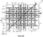
figures 2A-2B servent à illustrer un substrat semi-conducteur avec une structure de blocage de courant de Foucault mise en œuvre suivant un premier exemple de réalisation de la présente invention ; - La
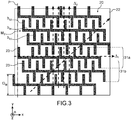
figure 3 sert à illustrer un deuxième exemple de réalisation de la présente invention ; - La
figure 4 sert à illustrer sert à illustrer un troisième exemple de réalisation de la présente invention ; - La
figure 5 sert à illustrer une variante de structure de blocage de courant de Foucault sous forme d'un agencement en damier de zones dopées N et P ; - La
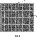
figure 6 sert à illustrer une autre variante de structure de blocage de courant de Foucault sous forme d'un agencement matriciel de zones dopées N ayant un motif rectangulaire et réalisées à l'intérieur d'un secteur globalement dopé P ; - La
figure 7 sert à illustrer une autre variante d'agencement matriciel de régions dopées N dans un secteur globalement dopé P ; - La
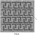
figure 8 sert à illustrer un agencement de régions dopées ayant un motif formé de plusieurs branches et réalisées à l'intérieur d'un secteur globalement dopé ayant un type de conductivité opposé à celui desdites régions ; - La
figure 9 sert à illustrer un agencement de régions dopées ayant un motif formé de plusieurs branches et réalisées à l'intérieur d'un secteur globalement dopé ayant un type de conductivité opposé à celui desdites régions ; - La
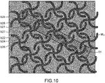
figure 10 sert à illustrer sert à illustrer un exemple de réalisation de structure de blocage de courants de Foucault suivant la présente invention, avec une portion d'antenne ou d'inductance en regard de cette structure ; - Les
figures 11A-11B servent à illustrer des exemples de composants RF destinés à être placé en regard d'une structure de blocage de courant de Foucault telle que mise en œuvre suivant l'invention; - Les
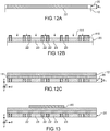
figures 12A, 12B, 12C servent à illustrer un procédé de fabrication d'un substrat de type semi-conducteur sur isolant muni d'une structure de blocage de courants de Foucault telle que mise en œuvre suivant un mode de réalisation de la présente invention ; - La
figure 13 sert à illustrer un dispositif microélectronique doté d'un substrat de type semi-conducteur sur isolant muni d'une structure de blocage de courants de Foucault dans la couche de support et en regard de laquelle un composant ou circuit RF est formé ; - La
figure 14 sert à illustrer un dispositif microélectronique doté d'un substrat avec une structure de blocage de courants de Foucault localisée dans une région, tandis qu'une autre région dépourvue de BOX est dédiée à un circuit doté de composants logiques ; - La
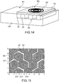
figure 15 sert à illustrer un agencement de régions dopées formé de plusieurs branches réalisant un motif en spirale à l'intérieur d'un secteur globalement dopé ayant un type de dopage opposé à celui desdites régions ; - Des parties identiques, similaires ou équivalentes des différentes figures portent les mêmes références numériques de façon à faciliter le passage d'une figure à l'autre.
- Les différentes parties représentées sur les figures ne le sont pas nécessairement selon une échelle uniforme, pour rendre les figures plus lisibles.
- Un exemple de réalisation d'une structure de blocage de courant parasites, en particulier de courants de Foucault, dans un substrat tel que mis en œuvre suivant un mode de réalisation de la présente invention, va à présent être donné en liaison avec les
figures 2A-2B (donnant respectivement une vue en coupe transversale du substrat avec la structure de blocage et une vue de dessus de cette structure). - La structure est réalisée dans une partie supérieure d'une couche de support 10 semi-conductrice d'un substrat, par exemple de type semi-conducteur sur isolant. Cette structure se présente sous forme d'un volume 20 dopé, de la couche 10 de support et est disposée contre, et de préférence en contact avec la couche isolante 11 du substrat. La couche isolante 11 est agencée sur la couche de support 10 et sépare cette couche de support 10 d'une couche semi-conductrice superficielle 12 dans laquelle des canaux de transistors peuvent être prévus.
- Le substrat peut être en particulier de type SOI (« Silicon On Insulator », i.e. « silicium sur isolant ») c'est-à-dire avec une couche semi-conductrice 12 superficielle en silicium.
- Par exemple, la couche superficielle semi-conductrice 12 peut être prévue avec une épaisseur comprise entre 4 nm et 50 nm. La couche isolante 11 est quant à elle typiquement à base d'oxyde de silicium et peut avoir une épaisseur comprise par exemple entre 15 nm et 250 nm.
- La couche de support 10 semi-conductrice peut être également en silicium et comporter sous le volume 20 dopé une couche de matériau semi-conducteur de résistivité élevée, par exemple supérieure à 1000cm, et avantageusement supérieure à 5000
 cm.
cm.
- Le volume 20 dopé peut quant à lui avoir une épaisseur e1 (dimension mesurée parallèlement à l'axe z d'un repère orthogonal [0;x;y;z] indiqué sur les figures) comprise par exemple entre 50 nm et 1 µm, avantageusement entre 100 nm et 500 nm.
- Le volume 20 dopé est ici formé d'un secteur dopé 22 selon un dopage d'un premier type, conférant un premier type de conductivité par exemple de type P, et d'une pluralité de régions 23 dopées. On prévoit dans la structure de blocage une répétition de régions dopées 23 distinctes entre elles réalisant un même motif M1, M'1 identique en termes de taille et de forme.
- Par « distinctes » on entend ici des régions non contiguës entre elles ou qui ne se touchent pas, et qui sont entourées par ledit secteur 22. Les régions dopées 23 ont un dopage d'un deuxième type, conférant un deuxième type de conductivité opposé audit premier type de conductivité, par exemple de type N. Par dopage de type N, on entend un dopage qui consiste à installer un excès d'électrons, tandis que par dopage de type P, on entend un dopage qui consiste à installer un excès de trous. On a donc, dans cet exemple, un secteur 22 dopé P et des régions 23 dopées N qui sont entourées par ce secteur 22.
- Les régions 23 dopées sont ainsi entourées, de préférence entièrement entourées, de portions dudit secteur dopé 22 ayant un dopage de type opposé. Le volume 20 comporte ainsi des jonctions 25a, 25b PN ou NP formées chacune, entre d'une part une zone du secteur 22 dopé selon ledit dopage du premier type et d'autre part une desdites régions dopées 23 selon le dopage du deuxième type ou inversement.
- Une telle disposition participe à limiter voire empêcher la propagation de courant de Foucault parasite du type de celui référencé C1 sur la
figure 5 . Dans un tel agencement en damier illustré sur cettefigure 5 , un courant parasite est en effet susceptible de traverser des régions dopées contiguës selon une diagonale, par rapport aux rangées longitudinales et transversales du damier. - Dans l'exemple de réalisation particulier des
figures 2A-2B , la succession de motifs dopés est telle que les régions dopées 23 sont réparties de manière périodique dans la structure sur au moins une rangée 31, 32, 33. Ces régions 23 peuvent être, elles-mêmes disposées sur plusieurs rangées agencées parallèlement à un premier axe Δ1, cet axe Δ1 étant parallèle à un plan principal du substrat. Par « plan principal » du substrat, on entend ici un plan passant par le substrat et qui est parallèle au plan [O;x;y] donné sur les figures. - Un agencement matriciel de régions dopées 23 réparties en lignes et en colonnes peut être en particulier prévu. Ainsi, dans l'exemple de réalisation particulier illustré, les régions dopées 23 sont également réparties en rangées 31 parallèlement à un deuxième axe Δ2, ce deuxième axe étant dans cet exemple parallèle au plan principal du substrat et orthogonal au premier axe Δ1.
- L'agencement périodique des régions 23 est tel que dans une première direction parallèle au premier axe Δ1, ladite structure comporte une ou plusieurs jonctions 25a, 25b, permettant de bloquer des courants parasites dans cette première direction, tandis que dans une deuxième direction orthogonale à la première direction et parallèle au deuxième axe Δ2, ladite structure comporte une ou plusieurs jonctions 25a, 25b permettant de bloquer des courants parasites dans cette deuxième direction, et que dans au moins une troisième direction parallèle à un troisième axe Δ3 et réalisant un angle non-nul, par exemple de 45°, avec lesdites première et deuxième directions et traversant ladite structure, ladite structure comporte une ou plusieurs jonctions 25a, 25b permettant de bloquer des courants parasites dans cette troisième direction.
- Dans la mesure où la longueur de propagation Ip des courants de Foucault dépend de la fréquence de fonctionnement du circuit RF, on adapte l'étendue (autrement dit l'empreinte ou la surface occupée) de la structure de blocage ou du volume dopée mesuré(e) dans un plan parallèle au plan principal du substrat, en fonction de celle du composant RF par exemple de type antenne ou inductance et de cette fréquence de fonctionnement. L'étendue de la structure de blocage est ainsi de préférence supérieure à celle de l'antenne et par exemple, pour une antenne de 30Ghz, un dépassement LD ≥ Ip d'au moins 1 mm, représentant la longueur maximale de propagation des courants de Foucault, est prévu.
- On prévoit également de préférence l'agencement des régions dopées 23 et leur taille de sorte qu'en regard de l'antenne, un segment de longueur égal à ladite longueur de propagation Ip est entrecoupé par au moins une jonction PN et au moins une jonction NP.
- Pour cela, on peut prévoir par exemple la longueur maximale des régions dopées 23, autrement dit la dimension maximale DM des motifs M1, M'1 mesurée parallèlement au plan [0 ;x ;y] du repère orthogonal [0;x;y;z] en fonction de la dimension Ip et de préférence de sorte que 2∗DM ≤ Ip. Typiquement, la dimension maximale DM est bien inférieure, c'est-à-dire au moins 10 fois inférieure aux dimensions de l'antenne et à la longueur Ip de propagation.
- Ainsi, un dispositif muni d'une telle structure de blocage présente un grand nombre de jonctions permettant de bloquer des courants parasites dans au moins 3 directions différentes (par exemple 45° de différence).
- Les régions dopées 23 de type N suivent de préférence un même motif M1, M'1. Dans l'exemple illustré, ce motif M1, M'1 est formé d'au moins une première branche b1 et d'au moins une deuxième branche b2 reliée à la première branche b1 et réalisant un angle non-nul avec la première branche b1. On se distingue ainsi de motifs de forme rectangulaire ou carré tels que par exemple ceux montrés sur les
figures 6 ,7 et qui, dans un agencement matriciel en damier favoriseraient la formation de chemins de courants parasites C'1, C'2. Avec une telle forme de motifs, on limite la possibilité de création de chemins de courants parasites. - La première branche b1 et/ou la deuxième branche b2 du motif M1, M'1 peut être prévue avec une dimension critique dc (dimension mesurée parallèlement au plan [0 ;x ;y] correspondant à la plus petite dimension d'un motif hormis son épaisseur) comprise par exemple entre 500 nm et 10 µm, avantageusement entre 1 µm et 5 µm
- Par exemple, on peut prévoir une dimension maximale DM comprise entre 5 µm et 100 µm, avantageusement entre 25 µm et 50 µm, tandis qu'un espace minimal dmin compris entre 500 nm et 10 µm, avantageusement entre 1 µm et 5 µm peut être prévu pour des pistes de largeur comprise entre 500 nm et 10 µm
- La répétition et la répartition en rangées des régions dopées 23 selon un motif ou selon une même séquence de motifs déterminé(e), permet de prévoir un composant RF ou circuit conducteur RF ou un élément conducteur en regard du volume 20 dopé sans nécessairement devoir réaliser un alignement précis de ce composant ou de ce circuit ou de cet élément conducteur par rapport aux jonctions et en particulier aux frontières des régions 23 dopées. La structure de blocage peut être ainsi avantageusement conçue sans nécessairement connaitre au préalable le dessin exact du circuit RF ou composant RF amené à être réalisé en regard du volume dopé 20. Les dimensions des pistes formant le circuit ou composant RF ainsi que l'encombrement global de ce composant ou de circuit peuvent alors suffire.
- Dans l'exemple de réalisation particulier illustré sur la
figure 2B , le motif M1, M'1 reproduit dans un agencement matriciel est un motif en forme de 'T', avec une alternance de rangées 32 dans lesquels le motif M1 présente une première orientation par rapport à l'axe Δ1 et de rangées 33 dans lesquels le motif M'1 suit une deuxième orientation, les motifs M1, M'1 d'une rangée 32 étant dans cet exemple d'agencement particulier disposés tête-bêche, c'est-à-dire selon une rotation de 180°, par rapport à ceux M'1 de la rangée 33 voisine. - Toutefois, d'autres agencements et formes de motifs peuvent être prévus. La
figure 2B permet d'illustrer un mode avantageux notamment par rapport à ceux illustrés sur lesfigures 8 et9 , où d'autres types de motifs en forme de 'L' et en forme de croix simple, ou de '+', ou de motif constitué de quatre branches sont utilisés. - Dans l'exemple de réalisation illustré sur la
figure 2B , l'agencement des motifs M1, M'1 et leur forme sont déterminés de sorte que quel que soit l'axe donné parallèle au premier axe Δ1, ou au deuxième axe Δ2 ou au troisième axe Δ3 traversant la structure et passant par une zone du secteur 22 entre deux régions dopées 23 voisines, cet axe donné rencontre une alternance de zones dopées de type N et de zone dopée de type P, avec au moins une jonction PN et au moins une jonction NP. Des chemins conducteurs parasites tels que ceux C3, C4 représentés de manière schématique sur lesfigures 8 et9 sont ainsi évités. - Un deuxième exemple de la structure de blocage est donné sur la
figure 3 . Il diffère de l'exemple précédemment décrit, notamment de par la forme des régions dopées 23, ainsi que de par leur répartition dans le secteur dopé 22. - Les régions dopées 23 ont ici un motif M2 identique répété, avantageusement de manière périodique, et de préférence selon un agencement matriciel dans lequel la répétition de motifs est réalisée sur plusieurs axes Δ1, Δ'2.
- Le motif M2 comporte, dans cet exemple particulier, une première branche b11, une deuxième branche b12 située à une première extrémité de la première branche b11 et une troisième branche b13 située à une deuxième extrémité de la première branche b11. Les branches b12 et b13 réalisent un angle non-nul, par exemple de 90° avec la première branche b11. Selon l'exemple illustré, la deuxième branche b12 et la troisième b13 présentent des directions d'allongement parallèles et selon des sens respectifs opposés. Autrement dit, le motif M2 n'est, ici, pas en forme de U. Un tel motif M2 à plusieurs branches s'étendant dans des directions différentes (par rapport à b11) participe à la mise en œuvre d'un blocage de courant dans plusieurs directions.
- Comme dans l'exemple précédent, un agencement régulier des régions 23 en lignes parallèles à un premier axe Δ1 est prévu. Toutefois, dans cet exemple de réalisation particulier, un décalage de positionnement des motifs est mis en œuvre entre des rangées voisines 31a, 31b successives parallèles au premier axe Δ1. Le décalage entre rangées voisines est ici un décalage pris par rapport à un plan P orthogonal au plan principal du substrat et orthogonal au premier axe Δ1.
- Ainsi, une rangée donnée 31a formée d'une succession de motifs M2, est, par rapport à un axe orthogonal au premier axe Δ1 décalé par rapport à une rangée voisine de ladite rangée donnée formée d'une autre succession dudit même motif donné M2. Une répartition des motifs M2 en rangées parallèles à un deuxième axe Δ'2 non-orthogonal au premier axe est ici réalisée.
- De par la forme et l'agencement des régions 23, en particulier leur répartition et la répétition périodique, la structure de blocage de courants parasites peut, comme dans l'exemple de réalisation précédent, être réalisée sans connaissance précise de l'agencement des pistes du circuit RF ou du composant RF. Par ailleurs, là encore, on met en œuvre un blocage selon au moins 3 directions distinctes, en particulier à au moins 45° les unes par rapport aux autres.
- Un troisième exemple de réalisation d'une structure de blocage est donné sur la
figure 4 . Il diffère de l'exemple précédent notamment de par la forme des régions dopées 23. - Les régions dopées 23 ont ici un motif M3 formé de quatre banches b21, b22, b23, b24 principales se rejoignant en une région d'intersection et de quatre branches b25, b26, b27, b28 secondaires chacune située à une extrémité respective d'une branche principale b21, b22, b23, b24, les branches secondaires b25, b26, b27, b28 suivant des orientations respectives différentes.
- Un tel motif M3 permet de faciliter un agencement dans lequel des branches de motifs voisins s'interpénètrent pour créer des zones du secteur dopé 22 selon le dopage du premier type et réalisant un parcours sinueux. Cela contribue à limiter voire empêcher la circulation de courants de Foucault.
- Dans l'exemple de réalisation illustré sur la
figure 4 , le motif a été représenté sans angle mais l'Homme du Métier saura adapter ce motif avec un angle, en particulier droit, entre une branche principale et sa branche secondaire afin de réaliser ce motif avec les techniques de lithographie dont on dispose actuellement. - Par exemple, le motif M3 est semblable à celui d'un svastika mais d'autres motifs à branches principales et secondaires peuvent être utilisés. Par exemple, on peut voir un motif dans lequel les branches principales réalisent entre elles un angle différent de 90° et/ou dans lequel les branches secondaires b25, b26, b27, b28 réalisent un angle différent de 90° avec les branches principales et/ou dans lequel d'autres branches dites « tertiaires » issues des branches secondaires réalisent un angle non-nul avec ses dernières.
- Comme dans l'exemple décrit précédemment, la répartition régulière selon un pas prédéterminé des motifs M3, permet de réaliser une structure de blocage permettant d'empêcher la circulation de courant de Foucault sans devoir connaitre nécessairement à l'avance la disposition des pistes conductrices d'un circuit RF ou d'un composant RF (tel qu'une antenne) destiné à être positionné en regard du volume dopé 20.
- Dans l'un ou l'autre des modes de réalisation précédemment décrits, il est possible de réaliser un secteur 22 dopé N tandis que les régions 23 situées à l'intérieur de ce secteur 22 sont dopées P. Inversement, on peut réaliser un secteur 22 dopé P tandis que les régions 23 intégrées dans ce secteur 22 sont dopées N.
- Dans l'exemple de réalisation illustré sur la
figure 4 comme dans les autres exemples de réalisation décrits précédemment, une structure de blocage qui comporte dans la première direction, dans la deuxième direction, dans la troisième direction : une succession de régions dopées formant ledit même motif donné identique en termes de forme, de dimensions, et éventuellement d'orientation par rapport à une direction donnée parmi lesdites première direction, deuxième direction, troisième direction est particulièrement avantageuse. On réalise un blocage optimal tout en évitant le problème d'alignement avec un composant passif ou une antenne. Selon une réalisation, une structure de blocage comporte dans la première direction, dans la deuxième direction, dans la troisième direction : une succession de régions dopées formant ledit même motif donné identique en termes de forme, de dimensions, et d'orientation par rapport à une direction donnée parmi lesdites première direction, deuxième direction, troisième direction. - Un autre exemple de réalisation d'une structure de blocage est donné sur la
figure 15 . Il diffère de par la forme des régions dopées 23. Les régions dopées 23 réalisent ici un motif M4 en forme de spirale composé d'une succession de branches b31, b32, b33, b34... distinctes d'orientations différentes entre elles. Les branches ici sous formes de spires ne se touchent pas entre elles, ni d'un motif M4 à l'autre. Les branches peuvent avoir une dimension critique par exemple de l'ordre de 100 nm, le motif en spirale ayant une dimension maximale par exemple de l'ordre de 1.5 µm, bien inférieur à celui d'un composant passif de type inductance ou antenne. - Dans l'exemple d'agencement illustré sur la
figure 10 (donnant une vue de dessus), une piste conductrice 51 par exemple d'une antenne ou d'une inductance, par laquelle un signal RF est destiné à transiter est positionnée au-dessus et en regard du volume dopé 20 dans lequel la succession répétée de jonctions PN et/ou NP est réalisée. Cette piste conductrice 51 peut être positionnée sans être nécessairement alignée avec et/ou sans tenir compte de l'orientation de l'une ou l'autre des branches b21, b22, b23, b24, b25, b26, b27, b28 du ou des motifs M3 de la structure de blocage. - Par exemple, la piste conductrice 51 peut être une portion d'inductance 160 réalisant une boucle de la forme d'un polygone tel qu'illustrée sur la
figure 11A ou celle globalement rectangulaire sur lafigure 11B . Dans ce cas, la connaissance de la surface occupée par l'inductance 160 et de la largeur de piste 60 permet de réaliser la structure 20 de blocage sans connaitre nécessairement l'orientation des pistes conductrices par rapport aux motifs dopés. - Un exemple de procédé de réalisation d'une structure de blocage de courants parasites pour substrat semi-conducteur sur isolant et qui peut être du type d'un des modes de réalisations précédemment décrits, va à présent être donné en liaison avec les
figures 12A-12C . - Un matériau de départ possible pour ce procédé est ici un substrat massif, autrement dit de type communément appelé « bulk » formé d'une tranche de matériau semi-conducteur. Le substrat massif est ici destiné à former la couche de support dans laquelle la structure de blocage est réalisée.
- Une couche superficielle de cette couche de support 10 peut être tout d'abord dopée, par exemple par implantation, pour réaliser le secteur dopé 22 (
figure 12A ). Pour cela, un dopage d'un premier type est effectué de sorte à former un secteur dopé 22. Par exemple, si l'on effectue un dopage à l'aide d'une espèce accepteuse, on réalise un secteur 22 ayant un dopage de type P. - Pour former un secteur 22 dopé P dans la couche de support 10, on peut par exemple effectuer une implantation de Bore selon une énergie comprise par exemple entre 10 keV et 150 keV, et une dose comprise par exemple entre 1014 cm-2 et 1015 cm-2.
- Ensuite, on prévoit un masque 110 à implantation comportant des ouvertures 111 distinctes reproduisant chacune un motif donné, par exemple l'un des motifs M1, M2, M3 décrits précédemment. Le masque 110 peut être par exemple à base de résine dans laquelle on pratique les ouvertures 111 par exemple au moyen d'un procédé de photolithographie.
- On forme ensuite les régions 23 dopées selon un dopage de type opposé. Par exemple, si l'on effectue une implantation à l'aide d'une espèce donneuse à travers les ouvertures 111 du masque 110, on peut réaliser des régions 23 ayant un dopage de type N (
figure 12B ) dans les parties exposées par les ouvertures 111. - Pour réaliser des régions 23 dopées N dans le secteur 22 dopé P, on peut par exemple effectuer une implantation de Phosphore selon une énergie comprise par exemple entre 20 keV et 200 keV, et une dose comprise par exemple entre 1014 cm-2 et 1015 cm-2.
- Selon un autre exemple de réalisation une implantation d'Arsenic selon une énergie comprise par exemple entre 40 keV et 200 keV, et une dose comprise par exemple entre 1014 cm-2 et 1015 cm-2 peut être effectuée pour former les régions 23.
- La dose utilisée pour former les régions dopées 23 est de préférence supérieure à celle du secteur dopé 22, afin de pouvoir inverser localement le type de conductivité dans les régions dopées 23 et pouvoir créer des régions dopées P dans un secteur globalement dopé N ou inversement des régions dopées N dans un secteur globalement dopé P.
- Le masque 110 peut être ensuite retiré. Par exemple, dans un cas où le masque 110 est à base de résine photosensible, on peut retirer ce masque 110 par gravure à l'aide d'un plasma d'oxygène et/ou d'un bain contenant un mélange d'acide sulfurique et d'eau oxygénée. Il peut avantageusement être utilisé un masque « dur », par exemple d'oxyde ou de nitrure de silicium, préalablement gravé par photolithographie et gravure, par exemple par plasma. Le masque dur peut ensuite être enlevé par voie chimique, en utilisant une solution de HF pour un masque en oxyde ou du H3PO4 pour un masque de nitrure.
- On peut ensuite former une couche isolante 11 sur la couche de support 10, par exemple par dépôt d'oxyde de silicium.
- Puis, on reporte une couche semi-conductrice 12 destinée à former la couche superficielle du substrat semi-conducteur sur isolant. Cette couche superficielle peut être réalisée par exemple par report d'un support semi-conducteur poignée, par exemple en silicium, que l'on colle sur la couche isolante 11 typiquement en effectuant un collage par adhérence moléculaire. Une couche d'oxyde peut être éventuellement prévue sur ce support poignée afin de réaliser un collage de type oxyde sur oxyde. Une zone de fragilisation est réalisée dans le support poignée par exemple en effectuant une implantation du support poignée. Ensuite, on peut effectuer une séparation d'une épaisseur du support poignée au niveau de la zone de fragilisation, de manière à conserver une autre épaisseur de ce support qui forme alors la couche semi-conductrice superficielle 12 (
figure 12C ). Ainsi, la couche superficielle 12 peut être réalisée à l'aide d'un procédé de type communément appelé Smart cut™. Le substrat semi-conducteur sur isolant est alors prêt à accueillir un ou plusieurs composants électroniques ainsi qu'au moins un composant RF ou circuit RF. - En variante de l'exemple de procédé qui vient d'être décrit, on peut former les jonctions directement dans la couche de support d'un substrat de type semi-conducteur sur isolant, par exemple à l'aide d'une première implantation pour réaliser le secteur dopé 22 puis une autre implantation à travers les ouvertures d'un masque pour réaliser les régions dopées 23.
- Une étape ultérieure de formation de pistes conductrices 60 de ce composant RF ou circuit RF par réalisation d'un premier niveau métallique est illustrée sur la
figure 12 . Le circuit RF est typiquement réalisé sur au moins deux niveaux de métallisation, avec une ou plusieurs pistes conductrices d'un premier niveau reliées à une ou plusieurs pistes conductrices d'un deuxième niveau. La structure de blocage formée de jonctions PN ou NP et telle que mise en œuvre suivant l'invention peut alors permettre d'empêcher la circulation de courants parasites susceptibles d'être générés par une circulation de courant sur chacun des niveaux de métallisation du circuit RF. - Comme cela a été décrit précédemment, une structure de blocage de courant de Foucault telle que mise en œuvre suivant l'invention peut être agencée sur un substrat de type semi-conducteur sur isolant, ou bien sur un substrat massif sur lequel une couche isolante est typiquement rajoutée.
- Dans un autre exemple de réalisation illustré sur la
figure 14 , le volume dopé 20 dans lequel la structure de blocage est réalisée, est formé dans la couche de support 100 semi-conductrice d'un substrat et en regard d'une région R2 sur laquelle s'étend une couche isolante 131 par exemple d'oxyde de silicium et d'épaisseur qui peut être comprise par exemple entre 50 nm et 1 µm Le composant RF 160, par exemple sous forme d'antenne, est agencé sur cette couche isolante 131, tandis qu'une autre région R1 de la couche de support 100 n'est, quant à elle, pas recouverte par la couche isolante 111. Cette autre région R2 peut être dédiée à d'autres types de composants et/ou circuits. Par exemple, on peut prévoir des composants logiques sur cette autre région R1.
Claims (15)
- Substrat pour dispositif RF, le substrat étant doté d'une couche superficielle semi-conductrice (12) disposée sur une couche isolante (11), la couche isolante étant agencée sur une couche de support (10) à base de matériau semi-conducteur, ladite couche de support étant dotée d'une structure (20) de blocage de courants de Foucault susceptibles d'être générés par un circuit RF destiné à être disposé sur le substrat, ladite structure de blocage étant formée d'une pluralité de jonctions (25a, 25b) pour bloquer une circulation de courants de Foucault, ladite structure (20) de blocage comprenant, dans un secteur dopé (22) selon un dopage d'un premier type, en particulier P ou N : une pluralité de régions (23) dopées distinctes ayant un dopage d'un deuxième type opposé au premier type, en particulier N ou P, lesdites régions dopées (23) ayant un dopage du deuxième type étant chacune entourées entièrement d'une zone dudit secteur dopé (22) et de dopage du premier type, et lesdites régions (23) ayant un dopage du deuxième type et réalisant chacune un motif donné (M1, M'1, M2, M3, M4,) formé d'au moins une première branche (b1, b11, b21, b31) et d'au moins une deuxième branche (b2, b12, b22, b32) réalisant un angle non-nul avec ladite première branche, ledit motif donné étant entouré entièrement de ladite zone dudit secteur dopé (22) et de dopage du premier type, le motif donné (M1, M'1, M2, M3) et la répartition desdites régions (23) dopées dans ledit secteur dopé étant prévus de sorte que : dans une première direction parallèle au premier axe (Δ1) et traversant ladite structure, ladite structure comporte une ou plusieurs première(s) jonction(s) (25a, 25b), dans une deuxième direction orthogonale à la première direction et traversant ladite structure ladite structure comporte une ou plusieurs deuxième(s) jonctions, dans au moins une troisième direction réalisant un angle non-nul avec ladite première et deuxième directions et traversant ladite structure, ladite structure comporte une ou plusieurs troisième(s) jonctions.
- Substrat selon la revendication 1, ladite structure (20) comportant dans ladite première direction et/ou dans ladite deuxième direction et/ou dans ladite troisième direction : une succession de régions dopées (23) ayant un dopage du deuxième type et réalisant ledit même motif donné identique.
- Substrat selon l'une des revendications 1 ou 2, lesdites régions dopées (23) distinctes étant réparties de manière périodique dans ladite structure sur une ou plusieurs première(s) rangée(s) (31, 31a, 31b) parallèlement à un premier axe (Δ1).
- Substrat selon la revendication 3, dans lequel lesdites régions dopées distinctes (23) sont réparties de manière périodique dans ladite structure sur une ou plusieurs autres rangées agencées parallèlement à un deuxième axe (Δ2), ledit premier axe (Δ1) et ledit deuxième axe (Δ2) étant parallèles audit plan principal, ledit deuxième axe (Δ2) réalisant un angle non-nul avec ledit premier axe.
- Substrat selon l'une des revendication 1 à 4, dans lequel ledit motif donné a une dimension maximale prévue inférieure et typiquement au moins deux fois inférieure, avantageusement au moins dix fois inférieure, à une dimension prédéterminée égale à une longueur maximale de propagation de courant de Foucault dans ledit matériau semi-conducteur de la couche de support à une fréquence de fonctionnement d'un circuit RF apte à être disposé en regard de l'antenne.
- Substrat selon l'une des revendications 1 à 5, la ou les premières rangées (31) étant formées d'une succession de régions dopées (23) comportant alternativement ledit motif donné (M1) suivant une première orientation et ledit motif donné (M'1) et suivant une deuxième orientation distincte de la première orientation.
- Substrat selon la revendication 6, comportant plusieurs autres rangées (32, 33) parallèlement au deuxième axe (Δ2), au moins une rangée (32) donnée étant formée d'une répétition dudit motif donné (M1) suivant la première orientation et au moins une rangée voisine de la rangée donnée étant formée d'une répétition dudit motif donné (M'1) suivant la deuxième orientation.
- Substrat selon l'une des revendications 1 à 7 dans lequel lesdites régions dopées distinctes (23) sont réparties de manière périodique dans ladite structure sur une ou plusieurs autres rangées parallèlement à un deuxième axe (Δ'2), le premier axe (Δ1) et ledit deuxième axe (Δ'2) étant des axes parallèles audit plan principal, ledit deuxième axe réalisant un angle inférieur à 90° avec ledit premier axe, parmi lesdites premières rangées au moins une rangée donnée étant formée d'une première succession de régions dopées reproduisant ledit motif donné, au moins une rangée voisine de ladite rangée donnée étant formée d'une deuxième succession de régions dopées reproduisant ledit motif donné, ladite rangée voisine étant décalée de ladite rangée donnée par rapport à un plan orthogonal au premier axe et audit plan principal.
- Substrat selon l'une des revendications 1 à 8, dans lequel ledit motif donné (M2) comporte une première branche (b11), une deuxième branche (b12) à une première extrémité de la première branche et réalisant un angle non-nul avec la première branche, et une troisième branche (b13) à une deuxième extrémité de la première branche et réalisant un angle non-nul avec la première branche (b11), la deuxième branche (b12) et la troisième branche (b13) ayant des orientations respectives différentes dans un plan parallèle à un plan principal de la couche de support (10).
- Substrat selon la revendication 9, dans lequel ledit motif donné (M3) comporte une première branche (b21) principale, une deuxième branche (b22) principale, une troisième branche (b23) principale, une quatrième branche (b24) principale, se rejoignant en un point d'intersection, et des branches secondaires (b25, b26, b27, b28) chacune située à une extrémité respective d'une branche principale, les branches secondaires (b25, b26, b27, b28) suivant des orientations respectives différentes dans un plan parallèle à un plan principal de la couche de support (10).
- Substrat selon l'une des revendications 1 à 9, dans lequel ledit motif donné (M4) est un motif en spirale comportant une succession de branches d'orientations respectives différentes.
- Dispositif microélectronique comprenant :- un substrat selon l'une des revendications 1 à 11,- un ou plusieurs composants électroniques, en particulier un ou plusieurs transistors au moins partiellement formés dans la couche superficielle dudit substrat,- au moins un circuit RF doté d'au moins un composant RF tel qu'une antenne ou une inductance ou un composant RF, ledit composant RF étant agencé en regard dudit secteur dopé (22).
- Procédé de fabrication d'un substrat selon l'une des revendications 1 à 12, le procédé comprenant les étapes suivantes :- réaliser un dopage d'un premier type d'au moins un secteur (22) d'un support semi-conducteur,- disposer un masque (110) en regard dudit secteur (22) dopé, le masque (110) comprenant des ouvertures (111) ayant une forme reproduisant ledit motif donné,- implanter des régions (23) dudit secteur (22) dopé à l'aide d'une espèce dopante de sorte à réaliser un dopage d'un deuxième type opposé au premier type.
- Procédé selon la revendication 13, comprenant après ladite implantation des régions (23), des étapes de :- formation d'une couche isolante (11) sur le support semi-conducteur, puis,- collage sur le support d'un support muni d'une couche semi-conductrice,- retrait d'une portion sacrificielle du substrat, tandis que la couche semi-conductrice est conservée et forme ladite couche semi-conductrice superficielle (12).
- Procédé de réalisation d'un dispositif RF selon la revendication 11 comprenant les étapes suivantes :- prévoir un substrat semi-conducteur sur isolant selon l'une des revendications 1 à 10 puis,- former ledit circuit conducteur RF ou ledit composant RF en regard dudit secteur (22) dopé.
Applications Claiming Priority (1)
| Application Number | Priority Date | Filing Date | Title |
|---|---|---|---|
| FR2002630A FR3108443B1 (fr) | 2020-03-18 | 2020-03-18 | Substrat rf avec jonctions ayant un agencement ameliore |
Publications (1)
| Publication Number | Publication Date |
|---|---|
| EP3882971A1 true EP3882971A1 (fr) | 2021-09-22 |
Family
ID=70918621
Family Applications (1)
| Application Number | Title | Priority Date | Filing Date |
|---|---|---|---|
| EP21161953.1A Pending EP3882971A1 (fr) | 2020-03-18 | 2021-03-11 | Substrat rf avec jonctions ayant un agencement amélioré |
Country Status (3)
| Country | Link |
|---|---|
| US (1) | US11362051B2 (fr) |
| EP (1) | EP3882971A1 (fr) |
| FR (1) | FR3108443B1 (fr) |
Families Citing this family (1)
| Publication number | Priority date | Publication date | Assignee | Title |
|---|---|---|---|---|
| US20250338518A1 (en) * | 2024-04-30 | 2025-10-30 | Nxp B.V. | Patterned deep trench isolation for passive devices |
Citations (5)
| Publication number | Priority date | Publication date | Assignee | Title |
|---|---|---|---|---|
| FR2808122A1 (fr) * | 2000-04-19 | 2001-10-26 | Mitsubishi Electric Corp | Dispositif a semiconducteurs et procede pour sa fabrication |
| US20040094822A1 (en) * | 2002-11-15 | 2004-05-20 | Jay Yu | Low substrate loss inductor |
| US20080020488A1 (en) * | 2006-07-18 | 2008-01-24 | International Business Machines Corporation | Semiconductor integrated circuit devices having high-Q wafer backside inductors and methods of fabricating same |
| US20110133308A1 (en) * | 2009-05-22 | 2011-06-09 | Chan Kuei-Ti | Semiconductor device with oxide define pattern |
| US20130320490A1 (en) * | 2012-06-05 | 2013-12-05 | Ertugrul Demircan | Inductive element with interrupter region and method for forming |
Family Cites Families (1)
| Publication number | Priority date | Publication date | Assignee | Title |
|---|---|---|---|---|
| US9449976B2 (en) * | 2013-12-12 | 2016-09-20 | Taiwan Semiconductor Manufacturing Co., Ltd. | Semiconductor device structure and method for manufacturing the same |
-
2020
- 2020-03-18 FR FR2002630A patent/FR3108443B1/fr active Active
-
2021
- 2021-03-11 EP EP21161953.1A patent/EP3882971A1/fr active Pending
- 2021-03-12 US US17/199,610 patent/US11362051B2/en active Active
Patent Citations (5)
| Publication number | Priority date | Publication date | Assignee | Title |
|---|---|---|---|---|
| FR2808122A1 (fr) * | 2000-04-19 | 2001-10-26 | Mitsubishi Electric Corp | Dispositif a semiconducteurs et procede pour sa fabrication |
| US20040094822A1 (en) * | 2002-11-15 | 2004-05-20 | Jay Yu | Low substrate loss inductor |
| US20080020488A1 (en) * | 2006-07-18 | 2008-01-24 | International Business Machines Corporation | Semiconductor integrated circuit devices having high-Q wafer backside inductors and methods of fabricating same |
| US20110133308A1 (en) * | 2009-05-22 | 2011-06-09 | Chan Kuei-Ti | Semiconductor device with oxide define pattern |
| US20130320490A1 (en) * | 2012-06-05 | 2013-12-05 | Ertugrul Demircan | Inductive element with interrupter region and method for forming |
Non-Patent Citations (1)
| Title |
|---|
| RACK ET AL.: "Low-Loss Si-Substrates Enhanced Using Buried PN Junctions for RF Applications", IEEE ELECTRON DEVICE LETTERS, vol. 40, no. 5, 2019, pages 690, XP011721119, DOI: 10.1109/LED.2019.2908259 |
Also Published As
| Publication number | Publication date |
|---|---|
| US20210296266A1 (en) | 2021-09-23 |
| US11362051B2 (en) | 2022-06-14 |
| FR3108443A1 (fr) | 2021-09-24 |
| FR3108443B1 (fr) | 2023-12-29 |
Similar Documents
| Publication | Publication Date | Title |
|---|---|---|
| US9312217B2 (en) | Methods for making a starting substrate wafer for semiconductor engineering having wafer through connections | |
| EP3502047B1 (fr) | Transistor fet à nanofil à resistance de contact reduite | |
| FR3086456A1 (fr) | Procede de realisation de transistors superposes | |
| KR101955375B1 (ko) | 3d 통합 프로세스들로 재료의 층들을 이동시키는 방법들 및 관련 구조들 및 디바이스들 | |
| EP2293327A1 (fr) | Circuit intégré à transistors MOS couplés électrostatiquement et procédé de réalisation d'un tel circuit intégré | |
| US20100289113A1 (en) | Fabrication process of a hybrid semiconductor substrate | |
| EP0581625B1 (fr) | Composant életronique multifonctions, notamment élément à résistance dynamique négative, et procédé de fabrication correspondant | |
| US20180233514A1 (en) | Semiconductor structure and method for manufacturing the same | |
| JP2011530826A (ja) | 埋め込み接地板を備えた半導体構造体の製造方法 | |
| FR2995137A1 (fr) | Dispositif microelectronique a tranchees d'isolation debordant sous une zone active | |
| US20090106726A1 (en) | Design structures including means for lateral current carrying capability improvement in semiconductor devices | |
| CN101553903B (zh) | 晶片通孔形成方法 | |
| FR3108443A1 (fr) | Substrat rf avec jonctions ayant un agencement ameliore | |
| EP0209419B1 (fr) | Procédé de réalisation d'au moins deux métallisations d'un composant semi-conducteur, recouvertes d'une couche de diélectrique, et composant obtenu par ce diélectrique | |
| US11901395B2 (en) | Insulation structure forming method | |
| TWI373838B (en) | Component with semiconductor junction and its production method | |
| US20080122096A1 (en) | Methods for lateral current carrying capability improvement in semiconductor devices | |
| US20140191359A1 (en) | Semiconductor-on-oxide structure and method of forming | |
| EP2447987B1 (fr) | Procédé de fabrication d'un substrat muni de deux zones actives avec des matériaux semi-conducteurs différents | |
| CN118471910A (zh) | 包括与埋入式电源轨连接的叉片器件的集成电路芯片 | |
| US10262898B2 (en) | Method for forming an electrical contact between a semiconductor film and a bulk handle wafer, and resulting structure | |
| EP3671836B1 (fr) | Circuit 3d dote d'une isolation mesa pour la zone de plan de masse | |
| FR2978611A1 (fr) | Procede ameliore de realisation de tranchees d'isolation dans un substrat semi-conducteur sur isolant | |
| CN114496921A (zh) | 半导体器件的制作方法以及半导体器件 | |
| EP3832707A1 (fr) | Structure d'interconnexion d'un circuit intégré |
Legal Events
| Date | Code | Title | Description |
|---|---|---|---|
| PUAI | Public reference made under article 153(3) epc to a published international application that has entered the european phase |
Free format text: ORIGINAL CODE: 0009012 |
|
| STAA | Information on the status of an ep patent application or granted ep patent |
Free format text: STATUS: REQUEST FOR EXAMINATION WAS MADE |
|
| 17P | Request for examination filed |
Effective date: 20210311 |
|
| AK | Designated contracting states |
Kind code of ref document: A1 Designated state(s): AL AT BE BG CH CY CZ DE DK EE ES FI FR GB GR HR HU IE IS IT LI LT LU LV MC MK MT NL NO PL PT RO RS SE SI SK SM TR |
|
| STAA | Information on the status of an ep patent application or granted ep patent |
Free format text: STATUS: EXAMINATION IS IN PROGRESS |
|
| 17Q | First examination report despatched |
Effective date: 20231127 |
|
| RAP3 | Party data changed (applicant data changed or rights of an application transferred) |
Owner name: COMMISSARIAT A L'ENERGIE ATOMIQUE ET AUX ENERGIESALTERNATIVES |
|
| REG | Reference to a national code |
Ref country code: DE Ref legal event code: R079 Free format text: PREVIOUS MAIN CLASS: H01L0027120000 Ipc: H10D0086010000 |
|
| GRAP | Despatch of communication of intention to grant a patent |
Free format text: ORIGINAL CODE: EPIDOSNIGR1 |
|
| STAA | Information on the status of an ep patent application or granted ep patent |
Free format text: STATUS: GRANT OF PATENT IS INTENDED |
|
| INTG | Intention to grant announced |
Effective date: 20250930 |
|
| RIC1 | Information provided on ipc code assigned before grant |
Ipc: H10D 86/01 20250101AFI20250919BHEP Ipc: H10D 86/00 20250101ALI20250919BHEP |