EP3879807A1 - Kameraanordnung für kraftfahrzeuge und verfahren zu deren montage - Google Patents
Kameraanordnung für kraftfahrzeuge und verfahren zu deren montage Download PDFInfo
- Publication number
- EP3879807A1 EP3879807A1 EP20382176.4A EP20382176A EP3879807A1 EP 3879807 A1 EP3879807 A1 EP 3879807A1 EP 20382176 A EP20382176 A EP 20382176A EP 3879807 A1 EP3879807 A1 EP 3879807A1
- Authority
- EP
- European Patent Office
- Prior art keywords
- housing
- insulating member
- camera assembly
- chamber
- electronics carrier
- Prior art date
- Legal status (The legal status is an assumption and is not a legal conclusion. Google has not performed a legal analysis and makes no representation as to the accuracy of the status listed.)
- Granted
Links
- 238000000034 method Methods 0.000 title claims abstract description 6
- 239000011810 insulating material Substances 0.000 claims abstract description 12
- 230000008021 deposition Effects 0.000 claims abstract description 4
- 230000003287 optical effect Effects 0.000 claims description 13
- 239000000463 material Substances 0.000 claims description 10
- 239000004020 conductor Substances 0.000 claims description 6
- 238000004891 communication Methods 0.000 claims description 4
- MTLMVEWEYZFYTH-UHFFFAOYSA-N 1,3,5-trichloro-2-phenylbenzene Chemical compound ClC1=CC(Cl)=CC(Cl)=C1C1=CC=CC=C1 MTLMVEWEYZFYTH-UHFFFAOYSA-N 0.000 description 34
- 239000000428 dust Substances 0.000 description 21
- 238000007789 sealing Methods 0.000 description 14
- 239000000945 filler Substances 0.000 description 6
- 239000003292 glue Substances 0.000 description 4
- 238000000151 deposition Methods 0.000 description 3
- 238000003384 imaging method Methods 0.000 description 3
- 230000004888 barrier function Effects 0.000 description 2
- 238000004519 manufacturing process Methods 0.000 description 2
- 239000011347 resin Substances 0.000 description 2
- 229920005989 resin Polymers 0.000 description 2
- 239000000853 adhesive Substances 0.000 description 1
- 230000001070 adhesive effect Effects 0.000 description 1
- 239000003570 air Substances 0.000 description 1
- 239000000969 carrier Substances 0.000 description 1
- 230000001010 compromised effect Effects 0.000 description 1
- -1 dirt Substances 0.000 description 1
- 239000007789 gas Substances 0.000 description 1
- 238000002955 isolation Methods 0.000 description 1
- 239000007788 liquid Substances 0.000 description 1
- 238000012986 modification Methods 0.000 description 1
- 230000004048 modification Effects 0.000 description 1
- 239000000843 powder Substances 0.000 description 1
- XLYOFNOQVPJJNP-UHFFFAOYSA-N water Substances O XLYOFNOQVPJJNP-UHFFFAOYSA-N 0.000 description 1
- 238000004078 waterproofing Methods 0.000 description 1
Images


Classifications
-
- B—PERFORMING OPERATIONS; TRANSPORTING
- B60—VEHICLES IN GENERAL
- B60R—VEHICLES, VEHICLE FITTINGS, OR VEHICLE PARTS, NOT OTHERWISE PROVIDED FOR
- B60R11/00—Arrangements for holding or mounting articles, not otherwise provided for
- B60R11/04—Mounting of cameras operative during drive; Arrangement of controls thereof relative to the vehicle
-
- H—ELECTRICITY
- H04—ELECTRIC COMMUNICATION TECHNIQUE
- H04N—PICTORIAL COMMUNICATION, e.g. TELEVISION
- H04N23/00—Cameras or camera modules comprising electronic image sensors; Control thereof
- H04N23/50—Constructional details
-
- H—ELECTRICITY
- H04—ELECTRIC COMMUNICATION TECHNIQUE
- H04N—PICTORIAL COMMUNICATION, e.g. TELEVISION
- H04N23/00—Cameras or camera modules comprising electronic image sensors; Control thereof
- H04N23/50—Constructional details
- H04N23/51—Housings
-
- H—ELECTRICITY
- H04—ELECTRIC COMMUNICATION TECHNIQUE
- H04N—PICTORIAL COMMUNICATION, e.g. TELEVISION
- H04N23/00—Cameras or camera modules comprising electronic image sensors; Control thereof
- H04N23/50—Constructional details
- H04N23/52—Elements optimising image sensor operation, e.g. for electromagnetic interference [EMI] protection or temperature control by heat transfer or cooling elements
-
- H—ELECTRICITY
- H04—ELECTRIC COMMUNICATION TECHNIQUE
- H04N—PICTORIAL COMMUNICATION, e.g. TELEVISION
- H04N23/00—Cameras or camera modules comprising electronic image sensors; Control thereof
- H04N23/57—Mechanical or electrical details of cameras or camera modules specially adapted for being embedded in other devices
Definitions
- This disclosure relates to a camera assembly for motor vehicles with improved sealing against dust and dirt.
- a method is also disclosed for assembling such camera assembly.
- Vehicle cameras typically include a housing inside of which an electronics carrier such as a printed circuit board (PCB) is provided.
- An image sensor or imager is connected to the electronics carrier.
- the image sensor is in turn in optical communication with a lens or lens assembly that is coupled to the camera housing.
- Light from the exterior is guided by the lens or lens assembly towards the image sensor or imager.
- the image that is captured by the image sensor is displayed on a display through a connector-adapter or electrical connector such as aitz Vietnamese Automobil (FAKRA) standard, automotive-grade connector. It is thus highly important that dust and dirt do not reach the image sensor.
- FAKRA a nursing Vietnamese Automobil
- Camera housings typically have a first opening for receiving the lens or lens assembly and a second opening for receiving the electrical connector.
- the first opening is typically sealed since by the lens or lens assembly being glued or screwed to the housing in a way that dust and dirt are prevented from entering the housing and contacting the image sensor.
- the second opening in many cases it is positioned such that there is little room for fitting a sealing means such as a rubber gasket or sealing cord. Also, sealing operation becomes awkward when the second opening is square shaped. This adds complexity and manufacturing costs while it can not be ensured that dust and dirt do not enter the housing and reach the image sensor.
- US2012019940 discloses a vehicle camera including a housing, a lens, and a lens barrel holding optical components therein.
- An image sensor is mounted on a printed circuit board (PCB) that is in turn mounted in the housing and positioned for receiving video input from the lens.
- the camera is configured to transmit to at least one other vehicular device signals relating to the video input received by the image sensor.
- the image sensor is protected from dust and dirt by a UV cured glue provided between the PCB and the housing.
- WO2018079300 discloses an imaging device that comprises a housing, an imaging unit fixed thereto by a curable resin including a curable adhesive.
- An image sensor is connected to a printed circuit board (PCB) which is mounted on the housing.
- the PCB is attached to a lens barrel.
- the housing is attached to an imaging unit-side mounting portion. Curable resin is provided in the holes where the screws are provided.
- the electrical components in the electronics carrier may not be affected by dust and dirt entering from the outside and can still operate, the image sensor may be greatly affected to the extent that the images displayed by a camera are not clear and thus be displayed blurred. This is aggravated in the case of metallic powder, as it is electrically conductive and could damage electronic components and even short-circuit the assembly. Image sensor isolation has not yet been fully resolved so a camera assembly for motor vehicles is required with enhanced sealing of the image sensor through a cost-effective sealing means.
- the present disclosure provides a camera assembly for motor vehicles whose configuration has been found to be cost-effective and highly efficient in sealing and protecting the imager or image sensor within the housing from foreign matter.
- the camera assembly that is herein disclosed comprises a housing having at least one opening for receiving a connector-adapter.
- the connector-adapter may be any standard automotive-grade connector of such as the above mentioned FAKRA electrical connector.
- Said opening in the housing may be preferably configured for receiving the connector-adapter or electrical connector in a way that a longitudinal axis of the connector-adapter is substantially perpendicular to an optical axis of a lens assembly. It may be preferred that a longitudinal axis of the connector-adapter is perpendicular to an optical axis of a lens assembly. However other relative orientations of connector-adapter longitudinal axis and lens assembly optical axis are possible.
- the housing of the camera assembly may be a one-piece housing, but it may preferably comprise at least a first housing part, or front housing, and a second housing part, or back housing, which together define an interior when attached to one another.
- the interior of the housing is suitable for containing therein an electronics carrier such as, for example, a printed circuit board (PCB), and an image sensor or imager connected to the electronics carrier.
- PCB printed circuit board
- the above mentioned lens assembly is optical communication with the image sensor for capturing an image.
- the lens assembly may be partly inserted into the housing or one of the housing parts.
- the housing is also an insulating member.
- the insulating member may for example be a paste-like element. Other configurations may however be possible.
- the insulating member is preferably fitted within the housing, arranged to contact inner walls of the housing and the electronics carrier.
- the insulating member is configured to define at least a first chamber and a second chamber within the housing. There is no constraint as to the relative size of volume of the chambers defined within the housing by the insulating member.
- the insulating member is arranged such that the electronics carrier is intersected by the insulating member. However, the electronics carrier and the insulating member are in electrical contact with each other, that is, electrical components in the electronics carrier received within the first chamber are in electrical contact with electrical components in the electronics carrier received within the second chamber. In other words, the insulating member does not interrupt the electrical connection between the electrical components in the electronics carrier. Such electrical contact may be either direct or indirect, that is, with other elements therebetween allowing the current to flow through.
- the connector-adapter is thus always electrically connected to the image sensor.
- the electronics carrier with its electrical components thus pass through the insulating member within the housing. It is preferred that the insulating member fits, surrounds and wraps a cross sectional portion of the electronics carrier and its components leaving no gaps between the insulating member and the electronics carrier and its components.
- the insulating member may be arranged perpendicular to the electronics carrier. Other relative angular positions of the insulating member and the electronics carrier are possible as long as the insulating member and the electronics carrier at least four areas or quadrants are defined within the housing.
- the electronics carrier has first and second main surfaces at least one of which is preferably flat. At least one portion of the first surface of the electronics carrier is located within the first chamber while at least another, different portion of the first surface of the electronics carrier is located within the second chamber. Both portions of the electronics carrier comprise electronic components electrically connected to each other. A stated above, the electronics carrier and the insulating member are in electrical contact with each other so that the insulating member does not interrupt the electrical connection between the electronic components of the electronics carrier.
- At least one portion of the second surface of the electronics carrier is located within the first chamber while at least another, different portion of the second surface of the electronics carrier is located within the second chamber.
- at least four areas or quadrants are defined within the housing by the relative positioning of the electronics carrier and the insulating member. According to what it has been stated above, said portions of the electronics carriers are in electrical connection with the insulating member.
- the insulating member may be made of a waterproofing material, liquids are not expected to be found within the camera assembly. However, dirt and dust, preferably suspended in air, may enter in the camera assembly through the opening for receiving the connector-adapter. In particular, through the gap between the edge of said opening for receiving the connector-adapter and the connector-adapter.
- dirt, dust are prevented from passing inside the housing where the image sensor is mounted, and more specifically, dirt, dust and other foreign matter are efficiently prevented from passing through the insulating member from the first chamber to the second chamber within the housing so foreign matter is prevented from reaching and come into contact with the image sensor when the image sensor is in the second chamber within the housing.
- a camera assembly with highly efficient sealing is provided due to the particular arrangement of the insulating member within the housing.
- sealing refers herein to a means which provides a tight and/or hermetic closure, preventing the passage of different materials such as dirt, dust, water, gas, air, etc. and in general foreign matter through a closure.
- the insulating member may comprise at least a first layer to be placed in the first housing part and a second layer to be placed in the second housing part.
- the electronics carrier in use, is sandwiched or otherwise inserted or interposed between the first layer and the second layer of the insulating member.
- the electronics carrier traverses, in use, the insulating member.
- the insulating member is preferably made of a material such that the first layer and the second layer are deformed under pressure when inserted in the first and second housing parts.
- a distance between oppositely facing surfaces of the first layer and the second layer of the insulating member is equal to or less than a thickness of the electronics carrier.
- At least one protrusion may be provided in the first and second housing parts adapted to receive the material of the insulating member. Such at least one protrusion is arranged extending at least substantially perpendicular to the main surfaces of the electronics carrier to support the insulating member.
- the protrusion may have at least one inclined portion, for example, an end portion, intended to abut inner walls of the housing.
- at least one protrusion may have at least one 60°-30° chamfered end such as for example a 45° chamfered end. Protrusions provide stability to the insulating member.
- Such chamfered end is suitable for a robot to apply paste-like insulating material from a source reservoir through 0.5 mm - 5 mm diameter supply needles in the robot onto the protrusion that is formed in front housing.
- the paste-like insulating material is applied in cords or droplets whose size substantially corresponds to the diameter of the robot supply needles.
- the height and the thickness of the first layer and the second layer of the insulating member is of the order of 0.5 mm - 5 mm such as for example 3 mm.
- This size is suitable to allow deformation of the first layer and the second layer in order to prevent gaps from being formed through the insulating member.
- greater cords or droplets would be required to be supplied. This may be performed by applying insulating material in several passes for each layer.
- the insulating member is preferred to be made of a thermally conductive material such as a commercially available gap filler. More specifically the insulating member is preferred to be made of a non-electrically conductive material having a thermal conductivity of, for example, 1-15 W/mK, more preferably 3-5 W/mK.
- a preferred thermally conductive material is one that dissipates heat generated by the electronics components in the electronics carrier at least 10 times faster than air, preferably 40 times faster than air.
- stable properties at temperatures ranging from -40C° to 150C° for the material of the insulating member are also preferred. Hardness and strength of the material from which the insulating member is made are not degraded over time.
- the present disclosure also refers to a method for assembling the above described camera assembly.
- the method comprises depositing, for example through a suitable robot, insulating material such as a commercially available non-electrically conductive paste-like gap filler.
- the insulating material is applied in one or more passes, depending on the thickness and the layers desired for the insulating member.
- the housing comprises a first housing part and a second housing part, i.e. when a two-piece housing is provided, one pass is applied to the first housing part defining a first layer of insulating member and another pass is applied to the second housing part defining a second layer of insulating member.
- the electronics carrier is then fitted in the first housing part and attached to it by means of screws, for example, such that the insulating member is intersected by the electronics carrier. Other attaching means are possible.
- the second housing part is then aligned with (the image sensor should be permanently aligned with the lens assembly).
- a rubber gasket or other suitable sealing means is fitted between the first housing part and second housing part and both housing parts are attached together for example by means of screws.
- the first layer of the insulating member in the first housing part and the second layer of the insulating member in the second housing part define an insulating member which in turn divides the interior of the housing into a first chamber and a second chamber.
- the opening for receiving the lens assembly and the interface between the first housing part and the second housing part are sealed by glue or other suitable sealing means which, together with the opening for receiving the connector-adapter which is sealed with the insulating member, results in foreign matter such as dust and dirt being efficiently blocked from contacting the image sensor.
- the image sensor is efficiently protected from damages and at least image quality is not compromised due to foreign matter such as dust and dirt. This is accomplished by a camera assembly whose manufacturing process is improved and cost effective since a simple configuration is obtained where space is maximized.
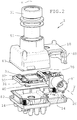
- a non-limiting example of a camera assembly 1 for motor vehicles is shown.
- the camera assembly 1 corresponds to a rear-view camera although many other different applications are possible.
- the camera assembly 1 comprises a housing that is formed by a first housing part, or front housing 10, and a second housing part, or back housing 20.
- the front housing 10 and the back housing 20 are attached together by means of screws 14 as shown in figure 2 .
- An interior is defined within the front housing 10 and the back housing 20 when attached to each other.
- a suitable rubber gasket is provided in an interface 80 between the front housing 10 and the back housing 20.
- the front housing 10 has a first opening 50 for receiving a lens assembly 51 as shown in the figures.
- the lens assembly 51 in the example shown is partly inserted into the front housing 10.
- an optical axis x is defined by the lens assembly 51.
- the first opening 50 is configured such that the lens assembly 51 is positioned in optical alignment with an image sensor or imager 40.
- a second opening 60 is provided for receiving a connector-adapter 61 such as of the FAKRA type, that is known in the field.
- a longitudinal axis y is defined by the connector-adapter 61.
- the second opening 60 is configured for receiving the connector-adapter 61 such that its longitudinal axis y is substantially perpendicular to the optical axis x of the lens assembly 51.
- the longitudinal axis y of the connector-adapter 61 is perpendicular to the drawing sheet of figure 1 , and thus also perpendicular to the optical axis x of the lens assembly 51.
- An electronics carrier 30 is mounted in the interior defined within the front housing 10 and the back housing 20.
- the electronics carrier is a printed circuit board (PCB) 30.
- the PCB 30 carries electrical components 35 including the above mentioned image sensor 40 such that it is in optical communication with the lens assembly 51 for capturing an image from the exterior of the vehicle that is displayed in a display by means the above connector-adapter 61.
- the insulating member 70 comprises a first layer 71 of insulating material and a second layer 72 of insulating material.
- the material from which the first layer 71 and the second layer 72 is made may be the same or different and may be for example a thermally conductive material such as a commercially available non-electrically conductive gap filler having a thermal conductivity of 1-15 W/mK that dissipates heat generated by the electronics components 35 in the PCB 30 at least 10 times faster than air, preferably 40 times faster than air, having stable properties at temperatures ranging from -20C° to 150C°.
- the PCB 30 has a first main flat surface 32 and an opposite second main flat surface 31 as depicted in figure 1 .
- a distance L between oppositely facing surfaces of the first layer 71 and the second layer 72 of the insulating member 70 is equal to or less than a thickness t of the electronics carrier 30.
- the insulating member 70 is positioned inside the front and back housing parts 10, 20 such that a first chamber 13a and a second chamber 13b are defined therein.
- the image sensor 40 is attached to the first main surface 32 of the PCB 30. The image sensor 40 is thus in the second chamber 13b. Due to the nature of the insulating member 70, the chambers 13a, 13b are effectively isolated such that dirt, dust and other foreign matter are prevented from passing through the insulating member 70 from the first chamber 13a to the second chamber 13b and thus from reaching the image sensor 40.
- the insulating member 70 is arranged surrounding and wrapping crosswise the PCB 30 and the electrical components 35 therein leaving no gaps there between. This allows space within of the camera assembly 1 to be advantageously optimized so more components can be fitted in the PCB 30.
- the PCB 30 is provided passing through the insulating member 70 such that they are arranged perpendicular to each other. With the insulating member 70 fitted to abut inner walls of the front and back housing parts 10, 20 and also the PCB 30 and its electrical components 35 sealing them results in dirt, dust and other foreign matter being prevented from reaching the image sensor 40 that is arranged in the second chamber 13b.
- a portion of an electronic component 35 is located in the first chamber 13a and another portion of the electronic component 35 is located in the second chamber 13b. Further, an intermediate part of said electronic component 35 is encapsulated between the insulating member 70 and the PCB 30.
- the insulating member 70 is made of a paste-like of thermally conductive material, said insulating member 70 is adapted to dissipate the heat generated by the electronic component 35.
- a height h of the electronic component 35 is lower than a distance d between the first main flat surface 32 and the protrusion 11. It is advantageous that the height h of the component 35 is less than 90% of the distance d between the first main flat surface 32 and the protrusion 11.
- the height h of the component 35 is less than 60% of the distance d between the first main flat surface 32 and the protrusion 11. Further, in the case that said electronic component 35 is arranged on the second main surface 31, its height h is lower than the distance d between the second main flat surface 31 and the protrusion 12.
- Quadrant Q1 is located within the first chamber 13a and is defined by the first main flat surface 32 of the PCB 30 and the second layer 72 of the insulating member 70.
- Quadrant Q1 comprises the second opening 60 for the connector-adapter 61.
- the second opening 60 is located in the first chamber 13a, either in the first quadrant Q1 or in the second quadrant Q2.
- the second opening 60 is arranged in both quadrants Q1, Q2.
- the adapter 61 may be electrically connected to at least one of the first main flat surface 32a of the first chamber 13a or to the second main flat surface 31a of the first chamber 13a.
- Quadrant Q2 is also located within the first chamber 13a and is defined by the second main flat surface 31 of the PCB 30 and the first layer 71 of the insulating member 70. Dust and dirt can enter the first chamber 13a even though although the electrical components 35 of the PCB 30 in the first chamber 13a are typically adapted to work under conditions with some dirt and dust.
- Quadrant Q3 is located within second chamber 13b and is defined by the first main flat surface 32 of the PCB 30 and the second layer 72 of the insulating member 70.
- Quadrant Q4 is also located within the second chamber 13b and is defined by the second main flat surface 31 of the PCB 30 and the first layer 71 of the insulating member 70.
- Quadrant Q4 includes the image sensor 40 having the optical connection with the lens assembly 51. Dust and dirt can not enter the second chamber 13b and thus can not reach the image sensor 40.
- the first and second main flat surfaces 32, 31 of the PCB 30 are each divided in corresponding first areas 32a, 31a and corresponding second areas 32b, 31b, respectively, according to quadrants Q1, Q2, Q3, Q4. More specifically, a first area 31a of the PCB second main surface 31 is defined within the first chamber 13a of the housing facing a wall of the front housing 10. A second area 31b of the PCB second main surface 31 that carries the image sensor 40 is defined within the second chamber 13b of the housing also facing said wall of the front housing 10. On the other hand, a corresponding first area 32a of the PCB first main surface 32 is defined within the first chamber 13a of the housing. A corresponding second area 32b of the PCB first main surface 32 is defined within the second chamber 13b of the housing opposite the image sensor 40.
- the lens assembly 51 is sealed in the first opening 50 through any suitable sealing means such as glue or the like.
- the interface 80 between the front housing 10 and the back housing 20 is also insulated by a rubber gasket or by any other suitable sealing means.
- This, together with the provision of the insulating member 70 within the front and back housings 10, 20 defines an insulated camera assembly 1 having therein a highly isolated chamber, i.e. the second chamber 13b, inside of which the image sensor 40 is mounted.
- the image sensor 40 fitted therein is fully protected and isolated from dirt, dust and any other foreign matter that otherwise could come into contact with it affecting images displayed.
- the front and back housings 10, 20 have respective inwardly projecting protrusions 11, 12 intended to receive insulating material of the first layer 71 and the second layer 72 of the insulating member 70 in order to provide stability for an efficient deposition of the material of the insulating member 70 in the front and back housings 10, 20.
- the protrusions 11, 12 are arranged extending perpendicular to the first and second main surfaces 31, 32 of the PCB 30. 45° chamfered ends 15 are defined in the protrusions 11, 12 intended to abut inner walls of the front and back housings 10, 20. Other inclinations for the ends 15 of the protrusions 11, 12 are envisaged such as 30-60°.
- Protrusions 11, 12 also allow the area of the first layer 71 and the second layer 72 of the insulating member 70 to be reduced.
- PCB supporting elements 33 are provided in inner side or perimetric walls of the front and back housings 10, 20 for supporting the PCB 30.
- the chamfered ends 15 extend from a position located below the PCB supporting elements 33 so as to avoid contact with the PCB 30.
- the chamfered ends 15 cause the first and second layers 71, 72 of the insulating member 70 to surround and wrap crosswise the PCB 30 and the electronic components 35.
- the PCB supporting elements 33 of the front housing may contact the first main flat surface 32 of the PCB 30.
- the PCB supporting elements 33 of the back housing may contact the second main flat surface 31 of the PCB 30.
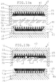
- a robot For assembling the camera assembly 1 described above, a robot deposits a paste-like gap filler or other suitable insulating material to define a first layer 71 of gap filler in the front housing 10 and a second layer 72 of gap filler in the back housing 20 so as to define an insulating member 70 that divides the interior of the front and back housings 10, 20 into two chambers 13a, 13b.
- This may be carried out applying insulating material in one or more passes 71a, 71b for the first layer 71 and one or more passes 72a, 72b for the second layer 72 of the insulating member 70 as shown in figures 13a, 13b and 14 .
- a PCB 30 with an image sensor or imager 40 connected thereto is then attached in the front housing 10 by means of the screws such that the image sensor 40 is optically connected to lens assembly 51.
- the screws are tightened so that the first main flat surface 32 of the PCB 30 contacts the PCB supporting elements 33 until it is seated thereon with the PCB 30 contacting the first layer 71 of the insulating member 70 which becomes deformed.
- the second main flat surface 31 of the PCB 30 then contacts the PCB supporting elements 33 until it is seated thereon.
- the first layer 71 of the insulating member 70 is pressed both by the PCB 30 and the protrusion 11 in the front housing 10.
- the PCB 30 is thus positioned perpendicular to the insulating member 70 dividing each chamber 13a, 13b into two sub-chambers as shown in figure 14 .
- the above mentioned four quadrants Q1, Q2, Q3, Q4 are defined within the front and back housings 10, 20 by the insulating member 70 and the PCB 30.
- the lens assembly 51 is then placed on a lens barrel defined in the first opening 50 formed in the front housing 10 and attached therein by UV cured glue or screwed.
- a rubber gasket may be preferably provided in the interface 80 of the front housing 10 and the back housing 20.
- the back housing 20 is then attached to the front housing 10 by means of screws 14 such that the back housing 20 is aligned with the front housing 10 as a result of which the image sensor 40 is also aligned with the lens assembly 51.
- the second layer 72 is thus pressed by the back housing 20 and the PCB 30 and becomes deformed contacting the first main flat surface 32 of the PCB 30 and also an upper portion of the electrical components 35 of the PCB 30 leaving no gaps.
- a barrier is formed by the insulating member 70 that prevents dust and/or dirt and other foreign matter in the first chamber 13a from passing to the second chamber 13b and reaching the image sensor 40.
Landscapes
- Engineering & Computer Science (AREA)
- Multimedia (AREA)
- Signal Processing (AREA)
- Physics & Mathematics (AREA)
- Electromagnetism (AREA)
- Mechanical Engineering (AREA)
- Studio Devices (AREA)
- Camera Bodies And Camera Details Or Accessories (AREA)
- Casings For Electric Apparatus (AREA)
- Cooling Or The Like Of Electrical Apparatus (AREA)
- Lens Barrels (AREA)
Priority Applications (4)
| Application Number | Priority Date | Filing Date | Title |
|---|---|---|---|
| EP20382176.4A EP3879807B1 (de) | 2020-03-11 | 2020-03-11 | Kameraanordnung für kraftfahrzeuge und verfahren zu deren montage |
| US17/198,778 US20210284081A1 (en) | 2020-03-11 | 2021-03-11 | Camera assembly for motor vehicles and method for assembling it |
| CN202110265446.7A CN113395420A (zh) | 2020-03-11 | 2021-03-11 | 用于机动车辆的摄像机组件及其组装方法 |
| JP2021038896A JP2021145334A (ja) | 2020-03-11 | 2021-03-11 | 自動車用カメラアセンブリおよびその組立方法 |
Applications Claiming Priority (1)
| Application Number | Priority Date | Filing Date | Title |
|---|---|---|---|
| EP20382176.4A EP3879807B1 (de) | 2020-03-11 | 2020-03-11 | Kameraanordnung für kraftfahrzeuge und verfahren zu deren montage |
Publications (2)
| Publication Number | Publication Date |
|---|---|
| EP3879807A1 true EP3879807A1 (de) | 2021-09-15 |
| EP3879807B1 EP3879807B1 (de) | 2023-12-20 |
Family
ID=69810767
Family Applications (1)
| Application Number | Title | Priority Date | Filing Date |
|---|---|---|---|
| EP20382176.4A Active EP3879807B1 (de) | 2020-03-11 | 2020-03-11 | Kameraanordnung für kraftfahrzeuge und verfahren zu deren montage |
Country Status (4)
| Country | Link |
|---|---|
| US (1) | US20210284081A1 (de) |
| EP (1) | EP3879807B1 (de) |
| JP (1) | JP2021145334A (de) |
| CN (1) | CN113395420A (de) |
Citations (6)
| Publication number | Priority date | Publication date | Assignee | Title |
|---|---|---|---|---|
| DE102005028144A1 (de) * | 2005-06-17 | 2006-12-28 | Robert Bosch Gmbh | Kameraanordnung mit Bildsensorabdichtung gegen Umwelteinflüsse |
| US20120019940A1 (en) | 2009-03-25 | 2012-01-26 | Magna Electronics Inc. | Vehicular camera and lens assembly |
| US20160191863A1 (en) * | 2014-12-31 | 2016-06-30 | Gentex Corporation | Rear vehicle camera |
| WO2018079300A1 (ja) | 2016-10-28 | 2018-05-03 | 日立オートモティブシステムズ株式会社 | 撮像装置 |
| US20180338070A1 (en) * | 2017-05-19 | 2018-11-22 | Magna Electronics Inc. | Vehicle camera with cast resin sealing |
| WO2019179545A1 (en) * | 2018-03-23 | 2019-09-26 | Sanezoo Se | Autonomous device for advanced image analysis, intelligent image recognition and image evaluation |
Family Cites Families (2)
| Publication number | Priority date | Publication date | Assignee | Title |
|---|---|---|---|---|
| JP2009086346A (ja) * | 2007-09-28 | 2009-04-23 | Fujifilm Corp | 電子機器用筐体及び撮像装置 |
| US11004767B2 (en) * | 2017-01-19 | 2021-05-11 | Sony Corporation | Composite material, electronic apparatus, and method for manufacturing electronic apparatus |
-
2020
- 2020-03-11 EP EP20382176.4A patent/EP3879807B1/de active Active
-
2021
- 2021-03-11 US US17/198,778 patent/US20210284081A1/en active Pending
- 2021-03-11 CN CN202110265446.7A patent/CN113395420A/zh active Pending
- 2021-03-11 JP JP2021038896A patent/JP2021145334A/ja active Pending
Patent Citations (6)
| Publication number | Priority date | Publication date | Assignee | Title |
|---|---|---|---|---|
| DE102005028144A1 (de) * | 2005-06-17 | 2006-12-28 | Robert Bosch Gmbh | Kameraanordnung mit Bildsensorabdichtung gegen Umwelteinflüsse |
| US20120019940A1 (en) | 2009-03-25 | 2012-01-26 | Magna Electronics Inc. | Vehicular camera and lens assembly |
| US20160191863A1 (en) * | 2014-12-31 | 2016-06-30 | Gentex Corporation | Rear vehicle camera |
| WO2018079300A1 (ja) | 2016-10-28 | 2018-05-03 | 日立オートモティブシステムズ株式会社 | 撮像装置 |
| US20180338070A1 (en) * | 2017-05-19 | 2018-11-22 | Magna Electronics Inc. | Vehicle camera with cast resin sealing |
| WO2019179545A1 (en) * | 2018-03-23 | 2019-09-26 | Sanezoo Se | Autonomous device for advanced image analysis, intelligent image recognition and image evaluation |
Also Published As
| Publication number | Publication date |
|---|---|
| JP2021145334A (ja) | 2021-09-24 |
| US20210284081A1 (en) | 2021-09-16 |
| CN113395420A (zh) | 2021-09-14 |
| EP3879807B1 (de) | 2023-12-20 |
Similar Documents
| Publication | Publication Date | Title |
|---|---|---|
| CN109588061B (zh) | 摄像装置模块 | |
| EP3430797B1 (de) | Kameraanordnung mit abgeschirmter bildgeberschaltung | |
| EP3240706B1 (de) | Fahrzeugrückfahrkamera | |
| KR100995237B1 (ko) | 환경 영향으로부터 밀봉되는 영상 센서를 구비한 카메라장치 | |
| US8970700B2 (en) | Imaging apparatus | |
| US20070051646A1 (en) | Waterproof case for in-vehicle camera | |
| JP7178993B2 (ja) | カメラモジュール及びカメラモジュール製造方法 | |
| US20210122299A1 (en) | Motor vehicle camera assembly | |
| JP2021067950A5 (de) | ||
| JP2010041709A (ja) | カメラモジュール | |
| WO2019049537A1 (ja) | 撮像装置 | |
| EP3879807A1 (de) | Kameraanordnung für kraftfahrzeuge und verfahren zu deren montage | |
| CN112821129B (zh) | 背板连接器组件及背板连接器用密封组件 | |
| US20230397347A1 (en) | Electronic device | |
| US8526196B2 (en) | Method for receiving an electric/electronic component and corresponding mounting method and covering for said type of device | |
| US11990667B2 (en) | On-vehicle radar apparatus | |
| US11927747B2 (en) | Camera module, vehicle camera and monitoring system | |
| JP7077129B2 (ja) | 筐体へのコネクタ組立体の取付構造 | |
| US20160116064A1 (en) | Sealing assembly between components | |
| CN210691020U (zh) | 拍摄设备、相机云台和可移动平台 | |
| CN107295220B (zh) | 适合于用在自动化车辆上的照相机 | |
| TW202331397A (zh) | 影像擷取裝置及用於製造影像擷取裝置之方法 | |
| CN116528026A (zh) | 摄像机以及图像传感装置 | |
| JP2022191884A (ja) | 防水装置 |
Legal Events
| Date | Code | Title | Description |
|---|---|---|---|
| PUAI | Public reference made under article 153(3) epc to a published international application that has entered the european phase |
Free format text: ORIGINAL CODE: 0009012 |
|
| STAA | Information on the status of an ep patent application or granted ep patent |
Free format text: STATUS: THE APPLICATION HAS BEEN PUBLISHED |
|
| AK | Designated contracting states |
Kind code of ref document: A1 Designated state(s): AL AT BE BG CH CY CZ DE DK EE ES FI FR GB GR HR HU IE IS IT LI LT LU LV MC MK MT NL NO PL PT RO RS SE SI SK SM TR |
|
| STAA | Information on the status of an ep patent application or granted ep patent |
Free format text: STATUS: REQUEST FOR EXAMINATION WAS MADE |
|
| 17P | Request for examination filed |
Effective date: 20220315 |
|
| RBV | Designated contracting states (corrected) |
Designated state(s): AL AT BE BG CH CY CZ DE DK EE ES FI FR GB GR HR HU IE IS IT LI LT LU LV MC MK MT NL NO PL PT RO RS SE SI SK SM TR |
|
| STAA | Information on the status of an ep patent application or granted ep patent |
Free format text: STATUS: EXAMINATION IS IN PROGRESS |
|
| 17Q | First examination report despatched |
Effective date: 20220714 |
|
| REG | Reference to a national code |
Ref document number: 602020023015 Country of ref document: DE Ref country code: DE Ref legal event code: R079 Free format text: PREVIOUS MAIN CLASS: H04N0005225000 Ipc: H04N0023500000 |
|
| RIC1 | Information provided on ipc code assigned before grant |
Ipc: B60R 1/00 20060101ALI20230504BHEP Ipc: H04N 23/52 20230101ALI20230504BHEP Ipc: H04N 23/51 20230101ALI20230504BHEP Ipc: H04N 23/50 20230101AFI20230504BHEP |
|
| GRAP | Despatch of communication of intention to grant a patent |
Free format text: ORIGINAL CODE: EPIDOSNIGR1 |
|
| STAA | Information on the status of an ep patent application or granted ep patent |
Free format text: STATUS: GRANT OF PATENT IS INTENDED |
|
| INTG | Intention to grant announced |
Effective date: 20230719 |
|
| GRAS | Grant fee paid |
Free format text: ORIGINAL CODE: EPIDOSNIGR3 |
|
| GRAA | (expected) grant |
Free format text: ORIGINAL CODE: 0009210 |
|
| STAA | Information on the status of an ep patent application or granted ep patent |
Free format text: STATUS: THE PATENT HAS BEEN GRANTED |
|
| AK | Designated contracting states |
Kind code of ref document: B1 Designated state(s): AL AT BE BG CH CY CZ DE DK EE ES FI FR GB GR HR HU IE IS IT LI LT LU LV MC MK MT NL NO PL PT RO RS SE SI SK SM TR |
|
| REG | Reference to a national code |
Ref country code: GB Ref legal event code: FG4D |
|
| REG | Reference to a national code |
Ref country code: CH Ref legal event code: EP |
|
| REG | Reference to a national code |
Ref country code: DE Ref legal event code: R096 Ref document number: 602020023015 Country of ref document: DE |
|
| REG | Reference to a national code |
Ref country code: IE Ref legal event code: FG4D |
|
| PG25 | Lapsed in a contracting state [announced via postgrant information from national office to epo] |
Ref country code: GR Free format text: LAPSE BECAUSE OF FAILURE TO SUBMIT A TRANSLATION OF THE DESCRIPTION OR TO PAY THE FEE WITHIN THE PRESCRIBED TIME-LIMIT Effective date: 20240321 |
|
| REG | Reference to a national code |
Ref country code: LT Ref legal event code: MG9D |
|
| PG25 | Lapsed in a contracting state [announced via postgrant information from national office to epo] |
Ref country code: LT Free format text: LAPSE BECAUSE OF FAILURE TO SUBMIT A TRANSLATION OF THE DESCRIPTION OR TO PAY THE FEE WITHIN THE PRESCRIBED TIME-LIMIT Effective date: 20231220 |
|
| REG | Reference to a national code |
Ref country code: NL Ref legal event code: MP Effective date: 20231220 |
|
| PG25 | Lapsed in a contracting state [announced via postgrant information from national office to epo] |
Ref country code: ES Free format text: LAPSE BECAUSE OF FAILURE TO SUBMIT A TRANSLATION OF THE DESCRIPTION OR TO PAY THE FEE WITHIN THE PRESCRIBED TIME-LIMIT Effective date: 20231220 |
|
| PG25 | Lapsed in a contracting state [announced via postgrant information from national office to epo] |
Ref country code: LT Free format text: LAPSE BECAUSE OF FAILURE TO SUBMIT A TRANSLATION OF THE DESCRIPTION OR TO PAY THE FEE WITHIN THE PRESCRIBED TIME-LIMIT Effective date: 20231220 Ref country code: GR Free format text: LAPSE BECAUSE OF FAILURE TO SUBMIT A TRANSLATION OF THE DESCRIPTION OR TO PAY THE FEE WITHIN THE PRESCRIBED TIME-LIMIT Effective date: 20240321 Ref country code: FI Free format text: LAPSE BECAUSE OF FAILURE TO SUBMIT A TRANSLATION OF THE DESCRIPTION OR TO PAY THE FEE WITHIN THE PRESCRIBED TIME-LIMIT Effective date: 20231220 Ref country code: ES Free format text: LAPSE BECAUSE OF FAILURE TO SUBMIT A TRANSLATION OF THE DESCRIPTION OR TO PAY THE FEE WITHIN THE PRESCRIBED TIME-LIMIT Effective date: 20231220 Ref country code: BG Free format text: LAPSE BECAUSE OF FAILURE TO SUBMIT A TRANSLATION OF THE DESCRIPTION OR TO PAY THE FEE WITHIN THE PRESCRIBED TIME-LIMIT Effective date: 20240320 |
|
| PGFP | Annual fee paid to national office [announced via postgrant information from national office to epo] |
Ref country code: DE Payment date: 20240327 Year of fee payment: 5 |
|
| REG | Reference to a national code |
Ref country code: AT Ref legal event code: MK05 Ref document number: 1643471 Country of ref document: AT Kind code of ref document: T Effective date: 20231220 |
|
| PG25 | Lapsed in a contracting state [announced via postgrant information from national office to epo] |
Ref country code: NL Free format text: LAPSE BECAUSE OF FAILURE TO SUBMIT A TRANSLATION OF THE DESCRIPTION OR TO PAY THE FEE WITHIN THE PRESCRIBED TIME-LIMIT Effective date: 20231220 |