EP3879641B1 - Steckverbinderanordnung zum elektrischen verbinden zweier kabel - Google Patents
Steckverbinderanordnung zum elektrischen verbinden zweier kabel Download PDFInfo
- Publication number
- EP3879641B1 EP3879641B1 EP20209820.8A EP20209820A EP3879641B1 EP 3879641 B1 EP3879641 B1 EP 3879641B1 EP 20209820 A EP20209820 A EP 20209820A EP 3879641 B1 EP3879641 B1 EP 3879641B1
- Authority
- EP
- European Patent Office
- Prior art keywords
- plug
- unit
- profile
- inner conductor
- mating
- Prior art date
- Legal status (The legal status is an assumption and is not a legal conclusion. Google has not performed a legal analysis and makes no representation as to the accuracy of the status listed.)
- Active
Links
Images
Classifications
-
- H—ELECTRICITY
- H01—ELECTRIC ELEMENTS
- H01R—ELECTRICALLY-CONDUCTIVE CONNECTIONS; STRUCTURAL ASSOCIATIONS OF A PLURALITY OF MUTUALLY-INSULATED ELECTRICAL CONNECTING ELEMENTS; COUPLING DEVICES; CURRENT COLLECTORS
- H01R13/00—Details of coupling devices of the kinds covered by groups H01R12/70 or H01R24/00 - H01R33/00
- H01R13/646—Details of coupling devices of the kinds covered by groups H01R12/70 or H01R24/00 - H01R33/00 specially adapted for high-frequency, e.g. structures providing an impedance match or phase match
- H01R13/6473—Impedance matching
-
- H—ELECTRICITY
- H01—ELECTRIC ELEMENTS
- H01R—ELECTRICALLY-CONDUCTIVE CONNECTIONS; STRUCTURAL ASSOCIATIONS OF A PLURALITY OF MUTUALLY-INSULATED ELECTRICAL CONNECTING ELEMENTS; COUPLING DEVICES; CURRENT COLLECTORS
- H01R24/00—Two-part coupling devices, or either of their cooperating parts, characterised by their overall structure
- H01R24/38—Two-part coupling devices, or either of their cooperating parts, characterised by their overall structure having concentrically or coaxially arranged contacts
- H01R24/40—Two-part coupling devices, or either of their cooperating parts, characterised by their overall structure having concentrically or coaxially arranged contacts specially adapted for high frequency
- H01R24/42—Two-part coupling devices, or either of their cooperating parts, characterised by their overall structure having concentrically or coaxially arranged contacts specially adapted for high frequency comprising impedance matching means or electrical components, e.g. filters or switches
- H01R24/44—Two-part coupling devices, or either of their cooperating parts, characterised by their overall structure having concentrically or coaxially arranged contacts specially adapted for high frequency comprising impedance matching means or electrical components, e.g. filters or switches comprising impedance matching means
-
- H—ELECTRICITY
- H01—ELECTRIC ELEMENTS
- H01R—ELECTRICALLY-CONDUCTIVE CONNECTIONS; STRUCTURAL ASSOCIATIONS OF A PLURALITY OF MUTUALLY-INSULATED ELECTRICAL CONNECTING ELEMENTS; COUPLING DEVICES; CURRENT COLLECTORS
- H01R24/00—Two-part coupling devices, or either of their cooperating parts, characterised by their overall structure
- H01R24/38—Two-part coupling devices, or either of their cooperating parts, characterised by their overall structure having concentrically or coaxially arranged contacts
-
- H—ELECTRICITY
- H01—ELECTRIC ELEMENTS
- H01R—ELECTRICALLY-CONDUCTIVE CONNECTIONS; STRUCTURAL ASSOCIATIONS OF A PLURALITY OF MUTUALLY-INSULATED ELECTRICAL CONNECTING ELEMENTS; COUPLING DEVICES; CURRENT COLLECTORS
- H01R13/00—Details of coupling devices of the kinds covered by groups H01R12/70 or H01R24/00 - H01R33/00
- H01R13/02—Contact members
- H01R13/22—Contacts for co-operating by abutting
- H01R13/24—Contacts for co-operating by abutting resilient; resiliently-mounted
- H01R13/2464—Contacts for co-operating by abutting resilient; resiliently-mounted characterized by the contact point
- H01R13/2478—Contacts for co-operating by abutting resilient; resiliently-mounted characterized by the contact point spherical
-
- H—ELECTRICITY
- H01—ELECTRIC ELEMENTS
- H01R—ELECTRICALLY-CONDUCTIVE CONNECTIONS; STRUCTURAL ASSOCIATIONS OF A PLURALITY OF MUTUALLY-INSULATED ELECTRICAL CONNECTING ELEMENTS; COUPLING DEVICES; CURRENT COLLECTORS
- H01R13/00—Details of coupling devices of the kinds covered by groups H01R12/70 or H01R24/00 - H01R33/00
- H01R13/46—Bases; Cases
- H01R13/502—Bases; Cases composed of different pieces
-
- H—ELECTRICITY
- H01—ELECTRIC ELEMENTS
- H01R—ELECTRICALLY-CONDUCTIVE CONNECTIONS; STRUCTURAL ASSOCIATIONS OF A PLURALITY OF MUTUALLY-INSULATED ELECTRICAL CONNECTING ELEMENTS; COUPLING DEVICES; CURRENT COLLECTORS
- H01R13/00—Details of coupling devices of the kinds covered by groups H01R12/70 or H01R24/00 - H01R33/00
- H01R13/62—Means for facilitating engagement or disengagement of coupling parts or for holding them in engagement
- H01R13/629—Additional means for facilitating engagement or disengagement of coupling parts, e.g. aligning or guiding means, levers, gas pressure electrical locking indicators, manufacturing tolerances
- H01R13/631—Additional means for facilitating engagement or disengagement of coupling parts, e.g. aligning or guiding means, levers, gas pressure electrical locking indicators, manufacturing tolerances for engagement only
-
- H—ELECTRICITY
- H01—ELECTRIC ELEMENTS
- H01R—ELECTRICALLY-CONDUCTIVE CONNECTIONS; STRUCTURAL ASSOCIATIONS OF A PLURALITY OF MUTUALLY-INSULATED ELECTRICAL CONNECTING ELEMENTS; COUPLING DEVICES; CURRENT COLLECTORS
- H01R13/00—Details of coupling devices of the kinds covered by groups H01R12/70 or H01R24/00 - H01R33/00
- H01R13/646—Details of coupling devices of the kinds covered by groups H01R12/70 or H01R24/00 - H01R33/00 specially adapted for high-frequency, e.g. structures providing an impedance match or phase match
- H01R13/6473—Impedance matching
- H01R13/6477—Impedance matching by variation of dielectric properties
-
- H—ELECTRICITY
- H01—ELECTRIC ELEMENTS
- H01R—ELECTRICALLY-CONDUCTIVE CONNECTIONS; STRUCTURAL ASSOCIATIONS OF A PLURALITY OF MUTUALLY-INSULATED ELECTRICAL CONNECTING ELEMENTS; COUPLING DEVICES; CURRENT COLLECTORS
- H01R13/00—Details of coupling devices of the kinds covered by groups H01R12/70 or H01R24/00 - H01R33/00
- H01R13/648—Protective earth or shield arrangements on coupling devices, e.g. anti-static shielding
- H01R13/658—High frequency shielding arrangements, e.g. against EMI [Electro-Magnetic Interference] or EMP [Electro-Magnetic Pulse]
- H01R13/6581—Shield structure
-
- H—ELECTRICITY
- H01—ELECTRIC ELEMENTS
- H01R—ELECTRICALLY-CONDUCTIVE CONNECTIONS; STRUCTURAL ASSOCIATIONS OF A PLURALITY OF MUTUALLY-INSULATED ELECTRICAL CONNECTING ELEMENTS; COUPLING DEVICES; CURRENT COLLECTORS
- H01R13/00—Details of coupling devices of the kinds covered by groups H01R12/70 or H01R24/00 - H01R33/00
- H01R13/648—Protective earth or shield arrangements on coupling devices, e.g. anti-static shielding
- H01R13/658—High frequency shielding arrangements, e.g. against EMI [Electro-Magnetic Interference] or EMP [Electro-Magnetic Pulse]
- H01R13/6591—Specific features or arrangements of connection of shield to conductive members
- H01R13/6592—Specific features or arrangements of connection of shield to conductive members the conductive member being a shielded cable
-
- H—ELECTRICITY
- H01—ELECTRIC ELEMENTS
- H01R—ELECTRICALLY-CONDUCTIVE CONNECTIONS; STRUCTURAL ASSOCIATIONS OF A PLURALITY OF MUTUALLY-INSULATED ELECTRICAL CONNECTING ELEMENTS; COUPLING DEVICES; CURRENT COLLECTORS
- H01R24/00—Two-part coupling devices, or either of their cooperating parts, characterised by their overall structure
- H01R24/38—Two-part coupling devices, or either of their cooperating parts, characterised by their overall structure having concentrically or coaxially arranged contacts
- H01R24/40—Two-part coupling devices, or either of their cooperating parts, characterised by their overall structure having concentrically or coaxially arranged contacts specially adapted for high frequency
-
- H—ELECTRICITY
- H01—ELECTRIC ELEMENTS
- H01R—ELECTRICALLY-CONDUCTIVE CONNECTIONS; STRUCTURAL ASSOCIATIONS OF A PLURALITY OF MUTUALLY-INSULATED ELECTRICAL CONNECTING ELEMENTS; COUPLING DEVICES; CURRENT COLLECTORS
- H01R4/00—Electrically-conductive connections between two or more conductive members in direct contact, i.e. touching one another; Means for effecting or maintaining such contact; Electrically-conductive connections having two or more spaced connecting locations for conductors and using contact members penetrating insulation
- H01R4/10—Electrically-conductive connections between two or more conductive members in direct contact, i.e. touching one another; Means for effecting or maintaining such contact; Electrically-conductive connections having two or more spaced connecting locations for conductors and using contact members penetrating insulation effected solely by twisting, wrapping, bending, crimping, or other permanent deformation
- H01R4/18—Electrically-conductive connections between two or more conductive members in direct contact, i.e. touching one another; Means for effecting or maintaining such contact; Electrically-conductive connections having two or more spaced connecting locations for conductors and using contact members penetrating insulation effected solely by twisting, wrapping, bending, crimping, or other permanent deformation by crimping
- H01R4/183—Electrically-conductive connections between two or more conductive members in direct contact, i.e. touching one another; Means for effecting or maintaining such contact; Electrically-conductive connections having two or more spaced connecting locations for conductors and using contact members penetrating insulation effected solely by twisting, wrapping, bending, crimping, or other permanent deformation by crimping for cylindrical elongated bodies, e.g. cables having circular cross-section
-
- H—ELECTRICITY
- H01—ELECTRIC ELEMENTS
- H01R—ELECTRICALLY-CONDUCTIVE CONNECTIONS; STRUCTURAL ASSOCIATIONS OF A PLURALITY OF MUTUALLY-INSULATED ELECTRICAL CONNECTING ELEMENTS; COUPLING DEVICES; CURRENT COLLECTORS
- H01R2103/00—Two poles
Definitions
- the invention relates to a connector arrangement for detachably connecting electrically conductive cables, in particular high-frequency cables, to an electrical component.
- high-frequency cables such as coaxial cables
- the coaxial arrangement of the inner conductor, dielectric, and shielding can largely ensure high signal transmission quality with low attenuation and low susceptibility to interference, provided the coaxial structure and the associated characteristic impedance remain largely constant over the entire length of the electrical cable.
- the cable ends, where connector systems are usually attached are often problematic. These are the ends of the cable that electrically and communicatively connect the cable to the components or other cables between which data transmission is to take place.
- connection systems which can be designed as plug-in couplings, have the disadvantage that a constant line characteristic impedance, especially at the connection point, is very difficult to achieve, since, for example, tolerances An air gap remains at the connection point between the two connecting partners, which can negatively impact the return loss and thus the transmission quality.
- the connection system must have a geometry that minimizes the risk of damage to the often very delicate cable ends during the connection process or normal cable operation.
- the EP 0 006 343 A1 discloses a connector assembly according to the preamble of claim 1, comprising a connector having a first connector housing with a cylindrical outer shell, a receptacle centered on the axis of the outer shell, and an insulating sleeve between the receptacle and the shell.
- the forward end of the insulating sleeve projects beyond the forward end of the receptacle and has peripheral portions defining a first male frustoconical surface.
- the coaxial connector has a second connector housing with a second cylindrical outer shell dimensioned to mate with the first outer shell, a contact pin centered on the axis of the second shell, and an insulating sleeve having portions defining complementary frustoconical surfaces to those at the forward end of the first connector housing.
- the convex surface of the connector helps eliminate misalignment between the plug and receptacle during mating of the first and second connector housings.
- the EP 3 460 916 A1 discloses an electrical contact device for an electrical cable, in particular a twin-axial cable, for the automotive sector, comprising an open crimping section, wherein, when the contact device is crimped onto the cable, a closed crimping section with an oval cross section is formed on the cable by means of the crimping section.
- a method for assembling an electrical cable for the automotive sector wherein, during the assembly of the cable, an open crimping section of an electrical contact device or an electrical connection device on the cable is converted into a closed crimping section on the cable, wherein, during the conversion of the open crimping section into the closed crimping section, a crimping section with an oval cross section and a closed crimping section is formed on the cable.
- the DE 10 2018 208532 A1 discloses a plug connection arrangement comprising a plug and a mating plug which can be plugged together with the plug along a plugging direction, wherein the impedance of the plug connection arrangement is constant at different plugging depths between the plug and the mating plug along the plugging direction.
- the EP 0 122 700 A2 discloses an electrical coaxial connector for connecting to a center conductor and a plurality of outer conductors of a coaxial cable, the coaxial connector comprising a center contact element that can be fastened to the center conductor and positioned within a bore of an inner dielectric element of an inner contact assembly. Furthermore, there is an inner contact element of the inner contact assembly and an outer contact assembly with an outer dielectric element having a bore in which the inner contact assembly is arranged, and an outer contact element to which an outer conductor of the plurality of outer conductors can be electrically connected.
- the outer contact element has a crimping portion and a sealing portion that can be positioned on an outer sheath of the cable and has a sealing element that is arranged within a recess of the sealing portion to form a seal between the sealing portion and the outer sheath of the cable.
- a crimping element is provided for connecting the inner conductor of the outer conductors to the inner contact element of the inner contact assembly, the inner contact assembly being arranged within the bore of the outer dielectric element.
- a crimp ring element is positionable for the cable along the crimp section, wherein the outer conductor of the plurality of outer conductors is positioned between the crimp ring element and the crimp section such that the crimp section can be crimped onto the crimp ring element such that the outer conductor is trapped therebetween.
- a plug connector assembly according to the invention is suitable for connecting a cable to an electrical component.
- an electrical component can be understood as meaning, for example, a semiconductor circuit board, but also another cable that is to be connected to the cable.
- the plug connector assembly according to the invention comprises a plug-in unit.
- the plug-in unit can be electrically conductively and preferably permanently connected to the cable or the electrical component and has an outer conductor element, an insulator element, and an inner conductor element.
- the plug connector assembly comprises a mating plug-in unit that can be electrically conductively and preferably detachably connected to the plug-in unit.
- the mating plug-in unit is electrically conductively connected, preferably permanently, to the electrical component or the cable that is to be connected to the plug-in unit.
- the mating plug-in unit likewise comprises an outer conductor element, an insulator element, and an inner conductor element.
- the insulator element of the plug-in unit is arranged within the outer conductor element of the plug-in unit.
- the insulator element of the plug-in unit has an inner conductor channel in which the inner conductor element of the plug-in unit is arranged.
- an inner conductor channel can be understood as a tubular passage in the insulator element.
- the mating plug-in unit has a comparable arrangement of outer conductor element, insulator element, and inner conductor element.
- the insulator element of the mating plug-in unit therefore also has an inner conductor channel.
- a described structure can be realized, for example, in that the outer conductor element of the plug-in unit and the mating plug-in unit are designed as a sleeve in which the preferably cylindrical insulator element is arranged.
- the inner conductor element is arranged in the inner conductor channel of the insulator element.
- the longitudinal axes of the inner conductor element, outer conductor element, and insulator element preferably run parallel in both the plug-in unit and the mating plug-in unit. It is particularly preferred that the inner conductor channel is arranged, in particular, centrally on the longitudinal axis of the insulator element in both the plug-in unit and the mating plug-in unit. However, a coaxial arrangement of the inner conductor element, outer conductor element, and insulator element is most preferred in both the plug-in unit and the mating plug-in unit.
- the plug-in unit has a first plug-in side.
- the first plug-in side can be understood as the side of the plug-in unit at which the plug-in unit can be connected, preferably detachably, to the mating plug-in unit.
- the insulator element of the plug-in unit forms, at least partially, a plug-in profile at one end facing the plug-in side.
- the plug-in profile is particularly preferably located on the front side of the Insulator element of the plug-in unit which faces the first plug-in side.
- the plug-in profile runs at least partially around the inner conductor channel and has at least one elevation and/or depression.
- the plug-in profile may have a plurality of elevations and depressions or a combination of one or more elevations and one or more depressions.
- the elevations and/or depressions preferably extend parallel to the longitudinal axis of the insulator element of the plug-in unit.
- the plug-in profile is preferably arranged in a ring around the inner conductor channel and can either be arranged at a distance from the inner conductor channel or be adjacent to the inner conductor channel.
- the mating plug unit has a second plug side.
- the second plug side can be understood to mean the side of the mating plug unit to which the mating plug unit can be connected, preferably detachably.
- the insulator element of the mating plug unit forms a mating plug profile at least partially at one end facing the second plug side.
- the mating plug profile is preferably arranged on an end face of the insulator element of the mating plug unit.
- the mating plug profile preferably also runs at least partially around the inner conductor channel of the insulator element of the mating plug unit and can be annular.
- the mating plug profile corresponds, at least in sections, to a negative form of the plug profile.
- the plug-in unit and the mating plug-in unit can be connected to one another in such a way that the plug-in profile and the mating plug-in profile abut one another at least in sections.
- the connection can be made, for example, by inserting the outer conductor elements of the plug-in unit and the mating plug-in unit into one another with the first and second plug-in sides facing one another, and by electrically connecting the inner conductor elements of the plug-in unit and the mating plug-in unit.
- the plug-in profile is partially formed by the inner conductor element of the plug-in unit.
- part of the plug-in profile is formed by the insulator element, and part of the plug-in profile is formed by the inner conductor element of the plug-in unit.
- the mating plug-in profile can be positioned not only particularly close to the insulator element of the plug-in unit, but also with the smallest possible distance to the inner conductor element of the plug-in unit when the plug-in unit and the mating plug-in unit are connected.
- the mating plug-in profile can also be partially formed by the inner conductor element of the mating plug-in unit.
- the inner conductor element of the plug-in unit and/or the mating plug-in unit have a profile section in the area of the plug-in profile. Within of the profile section, the inner conductor element has a specific shape that enables the plug-in profile and the mating plug-in profile to fit particularly close to each other.
- the connector assembly according to the invention provides a connection option, particularly for high-frequency cables, that ensures comparatively high signal quality. This is essentially due to the tight fit of the plug profile and the mating plug profile. Even in the case of large tolerance fluctuations, this ensures that no air gap can form between the two insulator elements extending all the way to the outer conductor. Fluctuations in the line impedance and the associated signal quality can thus be kept to a minimum, even with tolerance fluctuations.
- the profile section has a conical, parabolic and/or bulbous shape.
- the inner conductor element is a contact tip, it has proven particularly advantageous if the inner conductor element tapers in the profile section towards the plug-in side.
- the inner conductor element is a contact socket, it has proven advantageous if the inner conductor element widens in the profile section towards the plug-in side.
- the shape of the profile section is particularly preferably rotationally symmetrical about a central axis of the inner conductor element.
- the plug profile and/or the mating plug profile can have a chamfer that at least partially surrounds the inner conductor channel of the respective insulator element.
- the chamfer can be arranged either on an elevation or on a depression of the plug profile and/or the mating plug profile.
- the chamfer can be arranged on a side of the elevation and/or depression facing and/or away from the inner conductor channel.
- the chamfer can, for example, have an angle of 20 to 70 degrees. If the chamfer completely surrounds the inner conductor, an angle of 40 to 140 degrees can be enclosed by two opposing chamfers.
- the chamfer allows the plug profile and/or the mating plug profile to be used as a guide during the connection process, ensuring that all components are securely and electrically connected to one another even when the plug unit and mating plug unit are plugged together at an angle.
- the chamfer can also be arranged on an outer edge of the insulator element of the plug unit or mating plug unit.
- the chamfer is particularly preferably located on an outer edge of the end face of the insulator element of the Plug-in unit and/or counter-plug-in unit arranged, which faces the respective plug-in side.
- the inner conductor element of the plug-in unit can comprise a first contacting section that protrudes from the insulator element toward the first plug-in side. If the inner conductor element has a profile section, it is preferred that the first contacting section be adjacent to the profile section.
- the contacting section can be designed as a contact tip and have a length of 2.5 to 5 millimeters. Furthermore, the first contacting section can have a smallest diameter of the inner conductor element.
- the first contacting section can be inserted into the inner conductor channel of the insulator element of the mating plug unit and can be electrically connected to a second contacting section of the inner conductor element of the mating plug unit. If the first contacting section is designed as a contact tip, it is advantageous at this point if the second contacting section is configured as a contact socket. It can be particularly advantageous if an electrically conductive connection between the first and second contacting sections can only be created within the inner conductor channel of the insulator element of the mating plug unit.
- the inner conductor element of the mating plug unit can be recessed from the end of the insulator element of the mating plug unit facing the second plug side.
- the inner conductor element of the plug unit is first inserted into the inner conductor channel of the inner conductor element of the mating plug unit before the inner conductor element of the plug unit is electrically connected to the inner conductor element of the mating plug unit.
- the inner conductor element of the mating plug unit can be recessed by 0.4 to 1.2 millimeters from the end face of the insulator element facing the second plug side.
- the insulator element of the mating plug unit can have a funnel shape at the end facing the second plug side in the area of the inner conductor channel.
- the funnel shape can serve as a guide to ensure that when connecting the plug unit to the mating plug unit, the inner conductor elements of the plug unit and the mating plug unit are electrically connected.
- the funnel shape is particularly advantageous when the inner conductor element must first be inserted into the inner conductor channel of the insulator element of the mating plug unit in order to connect with the The inner conductor element of the mating plug unit is electrically connected.
- the funnel shape is round, and the center point of the funnel shape can be arranged on the longitudinal axis of the insulator element.
- the funnel shape can also at least partially form the mating plug profile.
- the funnel shape can have both linear and curved side walls.
- the funnel shape at least partially corresponds to the negative shape of the inner conductor element of the plug-in unit in the region of the plug profile.
- the insulator element in addition to the funnel shape, has a circumferential bevel on an outer edge, which partially forms the mating plug profile.
- the plug-in profile or the mating plug-in profile can have an annular recess surrounding the inner conductor element.
- the center of the annular recess lies on the longitudinal axis of the inner conductor channel.
- the annular recess can be partially formed by the inner conductor element.
- the annular recess can be round or square, with straight or curved surfaces.
- the outer conductor element, the inner conductor element, and the insulator element of the plug-in unit and/or the outer conductor element, the inner conductor element, and the insulator element of the mating plug-in unit are arranged coaxially to one another and have a common central axis. It is particularly preferred at this point that the plug-in profile and/or the mating plug-in profile have a concentric shape and/or a radially symmetrical shape relative to the central axis.
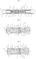
- FIG. 1 shows a first embodiment of a plug connector assembly 1 according to the invention in a sectional view.
- the sectional plane runs along a longitudinal axis of the plug connector assembly 1.
- the plug connector assembly 1 comprises a piercing unit 4 and a mating plug unit 5.
- the plug unit 4 is electrically conductively connected to a cable 2.
- the cable 2 is a coaxial cable.
- the mating plug element 5 is electrically conductively and permanently connected to an electrical component 3.
- the electrical component 3 is also a coaxial cable.
- the plug unit 4 and the mating plug unit 5 each consist of an outer conductor element 6, 7, an insulator element 8, 9 and an inner conductor element 10, 11.
- the insulator elements 8, 9 each have an inner conductor channel 12, 13.
- the outer conductor elements 6, 7 are designed as bronze sleeves, so that the insulator elements 8, 9 are arranged entirely within the outer conductor elements 6, 7.
- the insulator elements 8, 9 are made of plastic and have a cylindrical geometry.
- the bronze inner conductor elements 10, 11 are each arranged in the inner conductor channel 12, 13 of the insulator elements 8, 9.
- the outer conductor elements 6, 7 are each electrically conductively connected to a shield 27 and slipped over a dielectric 29 of the respective cable 2, 3.
- the inner conductor elements 10, 11 are crimped to strands 28 of the cables 2, 3.
- the shield 27 is formed by a wire mesh.
- the plug-in unit 4 has a first plug-in side 14, wherein the mating plug-in unit 5 has a second plug-in side 19.
- the plug-in unit 4 and the mating plug-in unit 5 are plugged into one another with the first and second plug-in sides 14, 19 facing one another.
- the outer conductor element 6 of the plug-in unit 4 has, in the area in which the plug-in unit 4 and the mating plug-in unit 5 are plugged into one another, have an outer diameter that is smaller than the inner diameter of the outer conductor element 7 of the mating plug-in unit 5 in the same area.
- the outer conductor element 7 of the mating plug-in unit 5 has a contact spring in order to fix the plug-in unit 4 in a force-fitting manner and to create a stable electrically conductive connection between the two outer conductor elements 6, 7.
- the plug-in unit 4 and the mating plug-in unit 5 are already plugged into one another.
- the outer conductor elements 6, 7, the insulator elements 8, 9 and the inner conductor elements 10, 11 of the plug-in unit 4 and the mating plug-in unit 5 are arranged with their longitudinal axes on a common central axis 26.
- FIG. 2 shows an enlarged view of the first embodiment of the plug connector assembly 1 according to the invention in a sectional view.
- the plug connector assembly 1 is in a plug-in position, with the plug-in unit 4 and the mating plug-in unit 5 positioned at the greatest possible distance from one another. This greatest possible distance can be caused, for example, by tolerances of the individual components or by a certain desired play between the components.
- the insulator element 8 of the plug-in unit 4 has a plug-in profile 16 on one end 15 facing the first plug-in side 14.
- the plug-in profile 16 is formed, on the one hand, by a recess 18 adjacent to the inner conductor channel 12 and extending annularly around the inner conductor channel 12.
- the plug-in profile 16 is formed by a profile section 22 of the inner conductor element 10.
- the insulator element 9 of the mating plug unit 5 has a mating plug profile 21 on an end face of an end 20 facing the second plug side 19.
- the mating plug profile 19 essentially corresponds to the negative shape of the plug profile 16.
- the insulator element 9 of the mating plug unit 5 has an elevation 17 on the end face which runs in a ring shape around the inner conductor channel 13.
- the inner conductor element 10 of the plug-in element 4 has a first contacting section 24, which adjoins the profile section 22 and is designed as a contact tip.
- the contact tip protrudes from the insulator element 8 of the plug-in unit 4 in the direction of the first plug-in side 14.
- the inner conductor element 10 tapers to a smaller outer diameter via the profile section 22 to the contacting section 24.
- the inner conductor element 11 of the mating plug-in unit 5 protrudes opposite the end face on the end 20 of the insulator element 9 facing the second plug-in unit, with the inner conductor channel 13 extending as far as the end face.
- the inner conductor element 11 of the mating plug-in unit 5 has a second contacting section 25, which is designed as a contact socket.
- the contact socket has an inner diameter that is larger than the outer diameter of the first contacting section 24 of the inner conductor element 10 of the plug-in unit 4.
- the first contacting section 24 is first inserted into the inner conductor channel 13 of the mating plug-in unit 5. The first contacting section 24 then dips into the second contacting section 25.
- FIG 3 shows a further illustration of the first embodiment of the plug connector assembly 1 according to the invention in a sectional view.
- the plug connector assembly 1 is also in the plug-in position, with the plug-in unit 4 and the mating plug-in unit 5 positioned at the smallest possible distance from one another due to tolerances.
- the first contacting section 24 is electrically conductively connected to the second contacting section 25.
- the plug-in profile 16 and the mating plug-in profile 21 bear against one another.
- the elevation 17 of the mating plug-in profile 21 thus conforms to the shape of the recess 18 of the plug-in profile 16.
- the inner conductor element 10 of the plug-in unit 4 has a bulbous shape in the profile section 22 that tapers towards the first contacting section 24, so that the profile section 22, together with the recess 18 in the insulator element 8, has an annular recess that runs around the inner conductor element 10 and whose center point is arranged on the central axis 26.
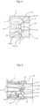
- Figure 4 shows a further enlarged illustration of the first embodiment of the plug connector assembly 1 according to the invention in a sectional view in the region of the plug profile 16 and the mating plug profile 21 in the plugged-in position.
- the mating plug profile 21 has a chamfer 23 on an outer edge of the end 20 of the insulator element 9 facing the second plug-in side 19, which chamfer extends from an outer surface of the insulator element 9 to the elevation 18.
- the recess 17 of the plug profile 16 has a complementary chamfer 23.
- the two insulator elements 8, 9 are guided towards one another, even when plugged together at a slight angle, which may be possible, for example, due to tolerances, in such a way that both insulator elements 8, 9 are at the latest when the
- the insulator element 9 of the mating plug-in unit 5 has a funnel shape on its front side, which extends around the inner conductor channel 13. The funnel shape ensures, on the one hand, that the mating plug-in profile 21 can at least partially form a negative shape of the plug-in profile 16, even in the area of the plug-in profile 16, which is formed by the profile section 22 of the inner conductor element 10.
- the funnel shape ensures that when the plug-in unit 4 and the mating plug-in unit 5 are plugged together, the inner conductor element 10 of the plug-in unit 4 can be guided into the inner conductor channel 13 of the insulator element 9 of the mating plug-in unit 5 without damage.
- FIG. 5 In a further illustration of the first embodiment of the connector assembly 1, a sectional view of the plugging process of the inner conductor element 10 of the plug-in unit 4 into the inner conductor channel 13 of the insulator element 9 of the mating plug-in unit 5 is shown. Although the plug-in unit 4 and the mating plug-in unit 5 are not plugged into one another exactly parallel, but rather slightly diagonally, the first contacting section 24 is guided into the inner conductor channel 13 of the insulator element 9 by the funnel shape. The risk of the inner conductor element 10 of the plug-in unit 4 being pressed against the insulator element 9 of the mating plug-in unit 5 and being deformed or even broken off can thus be significantly reduced.
Landscapes
- Details Of Connecting Devices For Male And Female Coupling (AREA)
- Coupling Device And Connection With Printed Circuit (AREA)
Description
- Die Erfindung betrifft eine Steckverbinderanordnung zum lösbaren Verbinden von elektrisch leitenden Kabeln, insbesondere Hochfrequenzkabeln, mit einem elektrischen Bauelement.
- Aufgrund der zunehmenden Digitalisierung von Komponenten und Systemen und der damit verbundenen steigenden Menge an zu übertragenden Daten werden in der heutigen Zeit immer größere Anforderungen an die zur Übertragung benötigten Kabel gestellt. Insbesondere eine gleichbleibend hohe Übertragungsqualität von Signalen über große Frequenzbereiche, bei geringer oder zumindest über den betreffenden Frequenzbereich konstanter Dämpfung, spielen bei der Übertragung von großen Datenmengen eine immer zentralere Rolle.
- Um diesen Anforderungen gerecht zu werden, kommen Hochfrequenzkabel, wie zum Beispiel Koaxialkabel zum Einsatz. Durch die koaxiale Anordnung von Innenleiter, Dielektrikum und Schirmung kann weitestgehend eine hohe Übertragungsqualität von Signalen bei geringer Dämpfung und geringer Störanfälligkeit sichergestellt werden, sofern der koaxiale Aufbau und der damit verbundene Leitungswellenwiderstand über die gesamte Länge der elektrischen Leitung weitestgehend konstant bleiben. Problematisch sind in diesem Zusammenhang jedoch häufig die Kabelenden, an denen in aller Regel Verbindungssysteme angebracht sind, um das Kabel mit den Komponenten oder weiteren Kabeln, zwischen denen die Datenübertragung erfolgen soll, elektrisch leitend und kommunizierend zu verbinden.
- Solche Verbindungssysteme, die beispielsweise als Steckkupplung ausgeführt sein können, besitzen jedoch den Nachteil, dass ein konstanter Leitungswellenwiderstand, insbesondere an der Verbindungsstelle nur sehr schwer erzielbar ist, da bspw. durch Toleranzen ein Luftspalt an der Verbindungsstelle zwischen beiden Verbindungspartnern verbleibt, der sich negativ auf die Rückflussdämpfung und damit die Übertragungsqualität auswirken kann. Gleichzeitig muss jedoch das Verbindungssystem eine Geometrie aufweisen, die das Risiko einer Beschädigung der oft sehr filigranen Enden der Kabel während des Verbindungsprozesses oder des Normalbetriebes des Kabels möglichst geringhalten.
- Die
EP 0 006 343 A1 offenbart eine Steckverbinderanordnung nach dem Oberbegriff des Anspruchs 1 mit einem Steckverbinder, der ein erstes Verbindergehäuse mit einer zylindrischen Außenhülle, einer Buchse, die auf der Achse der Außenhülle zentriert ist und einer Isolierhülse zwischen der Buchse und der Hülle aufweist. Das vordere Ende der Isolierhülse ragt über das vordere Ende der Buchse hinaus und hat periphere Bereiche, die eine erste männliche kegelstumpfförmige Fläche definieren. Der Koaxialsteckverbinder weist ein zweites Verbindergehäuse einer zweiten zylindrischen Außenhülle, die so dimensioniert ist, dass sie mit der ersten Außenhülle zusammenpasst, einem Kontaktstift, der auf der Achse der zweiten Hülle zentriert ist, und einer isolierenden Hülse, die Bereiche aufweist, die komplementäre kegelstumpfförmige Flächen zu denen am vorderen Ende des ersten Verbindergehäuses definieren. Im Gebrauch hilft die konvexe Fläche des Steckverbinders dabei, eine Fehlausrichtung zwischen dem Stecker und der Buchse während des Zusammensteckens des ersten und des zweiten Steckverbindergehäuses zu eliminieren. - Die
EP 3 460 916 A1 offenbart eine elektrische Kontaktvorrichtung für ein elektrisches Kabel, insbesondere ein Twinaxialkabel, für den Kraftfahrzeugbereich, umfassend einen offenen Crimpabschnitt, wobei in einem Crimpzustand der Kontaktvorrichtung auf dem Kabel, mittels des Crimpabschnitts ein geschlossener und in Querschnitten ovaler Crimpabschnitt auf dem Kabel eingerichtet ist. Ferner wird ein Verfahren zum Konfektionieren eines elektrischen Kabels für den Kraftfahrzeugbereich offenbart, wobei beim Konfektionieren des Kabels ein offener Crimpabschnitt einer elektrischen Kontaktvorrichtung oder einer elektrischen Verbindungseinrichtung auf dem Kabel in einen geschlossenen Crimpabschnitt auf dem Kabel übergeführt wird, wobei beim Überführen des offenen Crimpabschnitts in den geschlossenen Crimpabschnitt, ein in Querschnitten ovaler und geschlossener Crimpabschnitt auf dem Kabel eingerichtet wird. - Die
DE 10 2018 208532 A1 offenbart eine Steckverbindungsanordnung, umfassend einen Stecker und einen mit dem Stecker entlang einer Steckrichtung zusammensteckbaren Gegenstecker, wobei die Impedanz der Steckverbindungsanordnung bei verschiedenen Stecktiefen zwischen Stecker und Gegenstecker entlang der Steckrichtung konstant ist. - Die
EP 0 122 700 A2 offenbart einen elektrischen Koaxialverbinder zur Verbindung mit einem Mittelleiter und mehreren Außenleitern eines Koaxialkabels, wobei der Koaxialverbinder ein Mittelkontaktelement aufweist, das auf dem Mittelleiter befestigbar und innerhalb einer Bohrung eines inneren dielektrischen Elements einer inneren Kontaktanordnung positionierbar ist. Ferner ist ein inneres Kontaktelement der inneren Kontaktanordnung und eine äußere Kontaktanordnung mit einem äußeren dielektrischen Element, welches eine Bohrung besitzt, in der die innere Kontaktanordnung angeordnet ist, sowie ein äußeres Kontaktelement, mit dem ein Außenleiter der mehreren Außenleiter elektrisch verbindbar. Das äußere Kontaktelement weist einen Quetschabschnitt und einen Dichtabschnitt auf, die auf einer äußeren Hülle des Kabels positionierbar sind und ein Dichtelement besitzen, das innerhalb einer Ausnehmung des Dichtabschnitts angeordnet ist, um eine Abdichtung zwischen dem Dichtabschnitt und der äußeren Hülle des Kabels zu bilden, Ein Quetschelement ist zur Verbindung des Innenleiters der Außenleiter mit dem inneren Kontaktelement der inneren Kontaktanordnung vorgesehen, wobei die innere Kontaktanordnung innerhalb der Bohrung des äußeren dielektrischen Elements angeordnet ist. Ein Quetschringelement ist für das Kabel entlang des Quetschabschnitts positionierbar, wobei der Außenleiter der mehreren Außenleiter zwischen dem Quetschringelement und dem Quetschabschnitt positioniert ist, so dass der Quetschabschnitt auf das Quetschringelement derart aufquetschbar ist, dass der Außenleiter dazwischen gefangen ist. - Es ist daher eine Aufgabe der vorliegenden Erfindung, zumindest einen im Stand der Technik genannten Nachteil zu überwinden und eine lösbare Verbindungsanordnung zum Verbinden von Kabeln, insbesondere Hochfrequenzkabeln mit einem elektrischen Bauelement, wie beispielsweise einem weiteren Kabel oder einer Halbleiterplatine herzustellen, bei der die Übertragungsqualität der zu übertragenden Signale möglichst wenig beeinträchtigt wird.
- Die erfindungsgemäße Aufgabe wird durch eine Steckverbinderanordnung mit den Merkmalen des unabhängigen Anspruchs gelöst. Weitere vorteilhafte Ausgestaltungsformen der Erfindung lassen sich den Unteransprüchen, der Beschreibung sowie den Zeichnungen entnehmen.
- Eine erfindungsgemäße Steckverbinderanordnung ist zum Verbinden eines Kabels mit einem elektrischen Bauelement geeignet. Unter einem elektrischen Bauelement kann in diesem Zusammenhang beispielsweise eine Halbleiterplatine aber auch ein weiteres Kabel verstanden werden, das mit dem Kabel verbunden werden soll. Die erfindungsgemäße Steckverbinderanordnung umfasst eine Steckeinheit. Die Steckeinheit ist mit dem Kabel oder dem elektrischen Bauelement elektrisch leitend und bevorzugt unlösbar verbindbar und weist ein Außenleiterelement, ein Isolatorelement und ein Innenleiterelement auf. Des Weiteren umfasst die Steckverbinderanordnung eine Gegensteckeinheit, die elektrisch leitend und bevorzugt lösbar mit der Steckeinheit verbindbar ist. Die Gegensteckeinheit ist elektrisch leitend mit dem elektrischen Bauelement oder dem Kabel, bevorzugt unlösbar verbunden, dass mit der Steckeinheit verbunden werden soll. Die Gegensteckeinheit umfasst ebenfalls ein Außenleiterelement, ein Isolatorelement und ein Innenleiterelement.
- Das Isolatorelement der Steckeinheit ist innerhalb des Außenleiterelements der Steckeinheit angeordnet. Das Isolatorelement der Steckeinheit weist einen Innenleiterkanal auf, in dem das Innenleiterelement der Steckeinheit angeordnet ist. Unter Innenleiterkanal kann in diesem Zusammenhang ein röhrenförmiger Durchgang im Isolatorelement verstanden werden. Die Gegensteckeinheit weist eine vergleichbare Anordnung von Außenleiterelement, Isolatorelement und Innenleiterelement auf. Das Isolatorelement der Gegensteckeinheit weist also ebenfalls einen Innenleiterkanal auf. Ein beschriebener Aufbau kann beispielsweise realisiert sein, indem das Außenleiterelement von Steckeinheit und Gegensteckeinhalt als Hülse ausgebildet ist, in der das, bevorzugt zylinderförmige, Isolatorelement angeordnet ist. Das Innenleiterelement ist im Innenleiterkanal des Isolatorelements angeordnet. Die Längsachsen von Innenleiterelement, Außenleiterelement und Isolatorelement verlaufen bevorzugt sowohl bei der Steckeinheit als auch bei der Gegensteckeinheit vorzugsweise parallel. Besonders bevorzugt ist dabei, dass sowohl bei der Steckeinheit als auch bei der Gegensteckeinheit der Innenleiterkanal, insbesondere mittig auf der Längsachse des Isolatorelements angeordnet ist. Am meisten ist jedoch eine koaxiale Anordnung von Innenleiterelement, Außenleiterelement und Isolatorelement sowohl bei der Steckeinheit als auch bei der Gegensteckeinheit bevorzugt.
- Die Steckeinheit weist eine erste Steckseite auf. Unter der ersten Steckseite kann in diesem Zusammenhang die Seite der Steckeinheit verstanden werden, an der die Steckeinheit mit der Gegensteckeinheit, bevorzugt lösbar, verbindbar ist. Das Isolatorelement der Steckeinheit bildet an einem Ende, das der Steckseite zugewandt ist, zumindest teilweise ein Steckprofil aus. Das Steckprofil ist dabei besonders bevorzugt an der Stirnseite des Isolatorelements der Steckeinheit angeordnet, die der ersten Steckseite zugewandt ist. Das Steckprofil verläuft zumindest abschnittsweise um den Innenleiterkanal und weist zumindest eine Erhebung und/oder Vertiefung auf. Ebenso ist es möglich, dass das Steckprofil mehrere Erhebungen und Vertiefungen oder einer Kombination von einer oder mehreren Erhebungen und einer oder mehreren Vertiefungen aufweist. Die Erhebungen und/oder Vertiefungen erstrecken sich dabei bevorzugt parallel zur Längsachse des Isolatorelements der Steckeinheit. Das Steckprofil ist des Weiteren bevorzugt ringförmig um den Innenleiterkanal angeordnet und kann entweder im Abstand zum Innenleiterkanal angeordnet sein oder an den Innenleiterkanal angrenzen.
- Die Gegensteckeinheit weist eine zweite Steckseite auf. Unter der zweiten Steckseite kann in diesem Zusammenhang die Seite der Gegensteckeinheit verstanden werden, mit der die Gegensteckeinheit, bevorzugt lösbar, mit der der Steckeinheit verbindbar ist. Das Isolatorelement der Gegensteckeinheit bildet zumindest teilweise an einem Ende, das der zweiten Steckseite zugewandt ist, ein Gegensteckprofil aus. Das Gegensteckprofil ist bevorzugt auf einer Stirnseite des Isolatorelements der Gegensteckeinheit angeordnet. Das Gegensteckprofil verläuft bevorzugt ebenfalls zumindest teilweise um den Innenleiterkanal des Isolatorelements der Gegensteckeinheit und kann ringförmig ausgebildet sein. Das Gegensteckprofil entspricht zumindest abschnittsweise einer Negativform des Steckprofils.
- Die Steckeinheit und die Gegensteckeinheit sind derart miteinander verbindbar, dass das Steckprofil und das Gegensteckprofil zumindest abschnittsweise aneinander anliegen. Die Verbindung kann dabei beispielsweise erfolgen, indem die Außenleiterelemente der Steckeinheit und Gegensteckeinheit mit einander zugewandter erster und zweiter Steckseite ineinandergeschoben werden und sich die Innenleiterelemente der Steckeinheit und der Gegensteckeinheit elektrisch leitend miteinander verbinden.
- Das Steckprofil ist teilweise durch das Innenleiterelement der Steckeinheit ausgebildet. Es wird also ein Teil des Steckprofils vom Isolatorelement und ein Teil des Steckprofiles vom Innenleiterelement der Steckeinheit ausgebildet. Auf diese Weise kann das Gegensteckprofil sich nicht nur besonders dicht am Isolatorelement der Steckeinheit, sondern auch mit möglichst geringen Abstand am Innenleiterelement der Steckeinheit positioniert werden, wenn Steckeinheit und Gegensteckeinheit miteinander verbunden werden. Das Gegensteckprofil kann ebenfalls teilweise durch das Innenleiterelement der Gegensteckeinheit ausgebildet sein. Das Innenleiterelement der Steckeinheit und/oder der Gegensteckeinheit weisen im Bereich des Steckprofils einen Profilabschnitt auf. Innerhalb des Profilabschnitts weit das Innenleiterelement eine gezielte Formgebung auf, die ein besonders konturnahes aneinander Anliegen von Steckprofil und Gegensteckprofil ermöglicht.
- Durch die erfindungsgemäße Steckverbinderanordnung wird eine Verbindungsmöglichkeit, insbesondere für Hochfrequenzkabel bereitgestellt, bei der eine vergleichsweise hohe Signalqualität sichergestellt werden kann. Dies begründet sich im Wesentlichen durch das aneinander Anliegen des Steckprofils in das Gegensteckprofils. Auch im Fall von großen Toleranzschwankungen bleibt auf diese Art sichergestellt, dass zwischen beiden Isolatorelementen kein bis zum Außenleiter durchgängiger Luftspalt entstehen kann. Schwankungen im Leitungswellenwiderstand und damit verbunden in der Signalqualität können somit auch bei Toleranzschwankungen geringgehalten werden.
- Es kann in diesem Zusammenhang von Vorteil sein, wenn der Profilabschnitt, eine kegelförmige, parabolische und oder bauchige Form aufweist. Sofern es sich bei dem Innenleiterelement um eine Kontaktspitze handelt hat es sich als besonders vorteilhaft gewiesen, wenn sich das Innenleiterelement im Profilabschnitt in Richtung Steckseite verjüngt. Handelt es sich bei dem Innenleiterelement um eine Kontaktbuchse hat es sich als vorteilhaft erwiesen, wenn sich das Innenleiterelement im Profilabschnitt in Richtung Steckseite aufweitet. Die Form des Profilabschnitts ist dabei besonders bevorzugt rotationssymmetrisch um eine Mittelachse des Innenleiterelements ausgebildet.
- Das Steckprofil und/oder das Gegensteckprofil können eine Fase aufweisen, die den Innenleiterkanal des jeweiligen Isolatorelements zumindest teilweise umläuft. Die Fase kann sowohl an einer Erhebung als auch an einer Vertiefung des Steckprofils und/oder des Gegensteckprofils angeordnet sein. Die Fase kann dabei an einer dem Innenleiterkanal zugewandten und/oder abgewandten Seite der Erhebung und/oder Vertiefung angeordnet sein. Die Fase kann beispielsweise einen Winkel von 20 bis 70 Grad aufweisen. Sofern die Fase den Innenleiter vollständig umläuft, kann durch zwei gegenüberliegende Fasen ein Winkel von 40 bis 140 Grad eingeschlossen werden. Durch die Fase kann das Steckprofil und/oder das Gegensteckprofil während des Verbindungsprozesses als Führung genutzt werden, so dass auch bei einem schrägen Zusammenstecken von Steckeinheit und Gegensteckeinheit sichergestellt ist, dass alle Bauelemente sicher und elektrisch leitend miteinander verbunden werden. Die Fase kann auch an einer Außenkante des Isolatorelements der Steckeinheit oder Gegensteckeinheit angeordnet sein. Besonders bevorzugt ist die Fase dabei an einer Außenkante der Stirnseite des Isolatorelements der Steckeinheit und/oder Gegensteckeinheit angeordnet, die der jeweiligen Steckseite zugewandt ist.
- Das Innenleiterelement der Steckeinheit kann einen ersten Kontaktierungsabschnitt umfassen, der aus dem Isolatorelement in Richtung erster Steckseite hervorsteht. Sofern das Innenleiterelement einen Profilabschnitt aufweist, ist es bevorzugt, dass der erste Kontaktierungsabschnitt an den Profilabschnitt angrenzt. Der Kontaktierungsabschnitt kann als Kontaktspitze ausgeführt sein und eine Länge von 2,5 bis 5 Millimetern aufweisen. Weiterhin kann der erste Kontaktierungsabschnitt einen kleinsten Durchmesser des Innenleiterelements aufweisen.
- Der erste Kontaktierungsabschnitt kann in den Innenleiterkanal des Isolatorelements der Gegensteckeinheit einbringbar und mit einem zweiten Kontaktierungsabschnitt des Innenleiterelements der Gegensteckeinheit elektrisch leitend verbindbar sein. Sofern der erste Kontaktierungsabschnitt als Kontaktspitze ausgebildet ist, ist es an dieser Stelle von Vorteil, wenn der zweite Kontaktierungsabschnitt als Kontaktbuchse ausgestaltet ist. Es kann von besonderem Vorteil sein, wenn eine elektrisch leitende Verbindung zwischen ersten und zweiten Kontaktierungsabschnitt erst innerhalb des Innenleiterkanals des Isolatorelements der Gegensteckeinheit erzeugbar ist.
- Das Innenleiterelement der Gegensteckeinheit kann gegenüber dem der zweiten Steckseite zugewandten Ende des Isolatorelements der Gegensteckeinheit zurückstehen. In diesem Fall wird das Innenleiterelement der Steckeinheit zuerst in den Innenleiterkanal des Innenleiterelements der Gegensteckeinheit eingeführt, bevor das Innenleiterelement der Steckeinheit mit dem Innenleiterelement der Gegensteckeinheit elektrisch leitend verbunden wird. Das Innenleiterelement der Gegensteckeinheit kann gegenüber der Stirnseite des der zweiten Steckseite zugewandten Ende des Isolatorelements um 0,4 bis 1,2 Millimeter zurückstehen.
- Das Isolatorelement der Gegensteckeinheit kann an dem der zweiten Steckseite zugewandten Ende im Bereich des Innenleiterkanals eine Trichterform aufweisen. Die Trichterform kann als Führung dienen, um sicherzustellen, dass beim Verbinden der Steckeinheit mit der Gegensteckeinheit die Innenleiterelemente von Steckeinheit und Gegensteckeinheit elektrisch leitend verbunden werden. Die Trichterform ist besonders dann vorteilhaft, wenn das Innenleiterelement zuerst in den Innenleiterkanal der des Isolatorelements der Gegensteckeinheit eingeführt werden muss, um mit dem Innenleiterelement der Gegensteckeinheit elektrisch leitend verbunden zu werden. Vorzugsweise ist die Trichterform rund ausgebildet, wobei der Mittelpunkt der Trichterform auf der Längsachse des Isolatorelements angeordnet sein kann.
- Die Trichterform kann darüber hinaus das Gegensteckprofil zumindest teilweise ausbilden. Die Trichterform kann sowohl lineare als auch gekrümmte Seitenwände aufweisen. Weiterhin ist es bevorzugt, dass die Trichterform zumindest teilweise der Negativform des Innenleiterelements der Steckeinheit im Bereich des Steckprofils entspricht. In einer besonders bevorzugten Ausgestaltung weist das Isolatorelement zusätzlich zur Trichterform an einer Außenkante eine umlaufende Fase auf, die das Gegensteckprofil teilweise ausbildet.
- Das Steckprofil oder das Gegensteckprofil können eine das Innenleiterelement umlaufende Ringvertiefung aufweisen. Besonders bevorzugt liegt hierbei der Mittelpunkt der Ringvertiefung auf der Längsachse des Innenleiterkanals. Weiterhin kann die Ringvertiefung teilweise durch das Innenleiterelement ausgebildet sein. Die Ringvertiefung kann dabei sowohl rund als auch eckig mit geraden oder gekrümmten Flächen ausgebildet sein.
- In einer weiteren Ausgestaltung sind das Außenleiterelement, das Innenleiterelement und das Isolatorelement der Steckeinheit und/oder das Außenleiterelement, das Innenleiterelement und das Isolatorelement der Gegensteckeinheit koaxial zu einander angeordnet und weisen eine gemeinsame Mittelachse auf. Es ist an dieser Stelle besonders bevorzugt, dass das Steckprofil und/oder das Gegensteckprofil eine konzentrische Form und/oder radialsymmetrische Form zur Mittelachse aufweisen.
- Darüber hinaus sind weitere Vorteile und Merkmale der vorliegenden Erfindung aus der folgenden Beschreibung bevorzugter Ausführungsformen ersichtlich. Die dort und oben beschriebenen Merkmale können alleinstehend oder in Kombination umgesetzt werden, insofern sich die Merkmale nicht widersprechen. Die folgende Beschreibung der bevorzugten Ausführungsformen erfolgt dabei unter Bezugnahme auf die begleitenden Zeichnungen. Dabei zeigen:
- Figur 1
- eine erste Ausführungsform einer erfindungsgemäßen Steckverbinderanordnung in einer Schnittansicht;
- Figur 2
- eine vergrößerte Schnittansicht der ersten Ausführungsform;
- Figur 3
- eine vergrößerte Schnittansicht der ersten Ausführungsform in einer Steckposition;
- Figur 4
- eine vergrößerte Ansicht der ersten Ausführungsform im Bereich eines Steckprofils in Steckposition; und
- Figur 5
- eine vergrößerte Ansicht der ersten Ausführungsform im Bereich des Gegensteckprofils während eines Steckprozesses.
-
Figur 1 zeigt eine erste Ausführungsform einer erfindungsgemäßen Steckverbinderanordnung 1 in einer Schnittansicht. Die Schnittebene verläuft hierbei entlang einer Längsachse der Steckverbinderanordnung 1. Die Steckverbinderanordnung 1 umfasst eine Stecheinheit 4 und eine Gegensteckeinheit 5. Die Steckeinheit 4 ist mit einem Kabel 2 elektrisch leitend verbunden. Im vorliegenden Ausführungsbeispiel handelt es sich bei dem Kabel 2 um ein Koaxialkabel. Das Gegensteckelement 5 ist mit einem elektrischen Bauelement 3 elektrisch leitend und unlösbar verbunden. Im vorliegenden Ausführungsbeispiel handelt es sich bei der elektrischen Bauelement 3 ebenfalls um ein Koaxialkabel. Die Steckeinheit 4 und die Gegensteckeinheit 5 setzen sich jeweils aus einem Außenleiterelement 6, 7, einem Isolatorelement 8, 9 und einem Innenleiterelement 10, 11 zusammen. Die Isolatorelemente 8, 9 weisen jeweils einen Innenleiterkanal 12, 13 auf. Die Außenleiterelemente 6, 7 sind als Hülsen aus Bronze ausgeführt, so dass die Isolatorelemente, 8, 9 vollständig innerhalb der Außenleiterelemente 6, 7 angeordnet sind. Die Isolatorelemente 8, 9 bestehen aus Kunststoff und weisen eine zylinderförmige Geometrie auf. Die aus Bronze bestehenden Innenleiterelemente 10, 11 sind jeweils im Innenleiterkanal 12, 13 der Isolatorelemente 8, 9 angeordnet. Die Außenleiterelemente 6, 7 sind jeweils elektrisch leitend mit einer Schirmung 27 verbunden und über ein Dielektrikum 29 des jeweiligen Kabels 2, 3 gestülpt. Die Innenleiterelemente 10, 11 sind mit Litzen 28, der Kabel 2, 3 vercrimpt. In der vorliegenden Ausführungsform wird die Schirmung 27 durch ein Drahtgeflecht ausgebildet. - Die Steckeinheit 4 weist eine erste Steckseite 14 auf, wobei die Gegensteckeinheit 5 eine zweite Steckseite 19 aufweist. Die Steckeinheit 4 und die Gegensteckeinheit 5 sind mit einander zugewandter erster und zweiter Steckseite 14, 19 ineinandergesteckt. Das Außenleiterelement 6 der Steckeinheit 4 weist hierzu in dem Bereich, in dem die Steckeinheit 4 und die Gegensteckeinheit 5 ineinandergesteckt werden, einen Außendurchmesser auf, der kleiner ist als der Innendurchmesser das Außenleiterelement 7 der Gegensteckeinheit 5 in dem gleichen Bereich. Weiterhin weist das Außenleiterelement 7 der Gegensteckeinheit 5 eine Kontaktfeder auf, um die Steckeinheit 4 kraftschlüssig zu fixieren und eine stabile elektrisch leitende Verbindung zwischen beiden Außenleiterelementen 6, 7 herzustellen. In der dargestellten Ansicht sind Steckeinheit 4 und Gegensteckeinheit 5 bereits ineinandergesteckt. Die Außenleiterelemente 6, 7, die Isolatorelemente 8, 9 und die Innenleiterelemente 10, 11 der Steckeinheit 4 und der Gegensteckeinheit 5 sind im vorliegenden Ausführungsbeispiel mit Ihrer Längsachse auf einer gemeinsamen Mittelachse 26 angeordnet.
-
Figur 2 zeigt eine vergrößerte Darstellung der ersten Ausführungsform der erfindungsgemäßen Steckverbinderanordnung 1 in einer Schnittansicht. Die Steckverbinderanordnung 1 befindet sich in einer Steckposition, wobei die Steckeinheit 4 und die Gegensteckeinheit 5 im größtmöglichen Abstand zueinander positioniert sind. Dieser größtmögliche Abstand kann beispielsweise durch Toleranzen der einzelnen Bauteile oder durch ein gewisses gewünschtes Spiel zwischen den Bauteilen bedingt sein. Das Isolatorelement 8 der Steckeinheit 4 besitzt an einem der ersten Steckseite 14 zugewandten Ende 15 an einer Stirnseite ein Steckprofil 16. Das Steckprofil 16 wird in der vorliegenden Ausführungsform zum einen durch eine an den Innenleiterkanal 12 angrenzende und den Innenleiterkanal 12 ringförmig umlaufende Vertiefung 18 ausgebildet. Zum anderen wird das Steckprofil 16 durch einen Profilabschnitt 22 des Innenleiterelements 10 ausgebildet. Das Isolatorelement 9 der Gegensteckeinheit 5 besitzt an einer Stirnseite eines der zweiten Steckseite 19 zugewandten Ende 20 ein Gegensteckprofil 21. Das Gegensteckprofil 19 entspricht im Wesentlichen der Negativform des Steckprofils 16. Hierzu besitzt das Isolatorelement 9 der Gegensteckeinheit 5 an der Stirnseite eine Erhebung 17, die ringförmig um den Innenleiterkanal 13 verläuft. - Das Innenleiterelement 10 des Steckelements 4 besitzt einen ersten Kontaktierungsabschnitt 24, der sich an den Profilabschnitt 22 anschließt und als Kontaktspitze ausgebildet ist. Die Kontaktspitze steht von dem Isolatorelement 8 der Steckeinheit 4 in Richtung erster Steckseite 14 hervor. Weiterhin verjüngt sich das Innenleiterelement 10 über den Profilabschnitt 22 zum Kontaktierungsabschnitt 24 auf einen kleineren Außendurchmesser. Das Innenleiterelement 11 der Gegensteckeinheit 5 steht gegenüber der Stirnseite am der zweiten Steckeinheit zugewandten Ende 20 des Isolatorelements 9 zurück, wobei sich der Innenleiterkanal 13 bis zur Stirnseite hin erstreckt. Das Innenleiterelement 11 der Gegensteckeinheit 5 besitzt einen zweiten Kontaktierungsabschnitt 25, der als Kontaktbuchse ausgebildet ist. Die Kontaktbuchse weist einen Innendurchmesser auf, der größer ist als der Außendurchmesser des ersten Kontaktierungsabschnitts 24 des Innenleiterelements 10 der Steckeinheit 4. Um einen elektrisch leitenden Kontakt zwischen den Kontaktierungsabschnitten 24, 25 herstellen zu können, wird der erste Kontaktierungsabschnitt 24 zuerst in den Innenleiterkanal 13 der Gegensteckeinheit 5 eingeführt. Anschließende taucht der erste Kontaktierungsabschnitt 24 in den zweiten Kontaktierungsabschnitt 25 ein.
-
Figur 3 zeigt eine weitere Darstellung der ersten Ausführungsform der erfindungsgemäßen Steckverbinderanordnung 1 in einer Schnittansicht. In der gezeigten Darstellung befindet sich die Steckverbinderanordnung 1 ebenfalls in der Steckposition, die Steckeinheit 4 und die Gegensteckeinheit 5 im toleranzbedingten kleinstmöglichen Abstand zueinander positioniert sind. Der erste Kontaktierungsabschnitt 24 ist elektrisch leitend mit dem zweiten Kontaktierungsabschnitt 25 verbunden. Darüber hinaus liegen das Steckprofil 16 und das Gegensteckprofil 21 aneinander an. Die Erhebung 17 des Gegensteckprofils 21 schmiegt sich also an die Formgebung der Vertiefung 18 des Steckprofils 16 an. Das Innenleiterelement 10 der Steckeinheit 4 besitzt im Profilabschnitt 22 eine bauchige, sich zum ersten Kontaktierungsabschnitt 24 verjüngende Form, so dass der Profilabschnitt 22 zusammen mit der Vertiefung 18 im Isolatorelement 8 eine das Innenleiterelement 10 umlaufende Ringvertiefung besitzt , deren Mittelpunkt auf der Mittelachse 26 angeordnet ist. -
Figur 4 zeigt eine weitere vergrößerte Darstellung der ersten Ausführungsform der erfindungsgemäßen Steckverbinderanordnung 1 in einer Schnittansicht im Bereich des Steckprofils 16 und des Gegensteckprofils 21 in der Steckposition. Das Gegensteckprofil 21 besitzt an einer Außenkante des der zweiten Steckseite 19 zugewandten Endes 20 des Isolatorelements 9 eine Fase 23, die sich von einer äußeren Mantelfläche des Isolatorelements 9 bis zu der Erhebung 18 erstreckt. Die Vertiefung 17 des Steckprofils 16 weist eine komplementäre Fase 23 auf. Durch die Fase 23 sowohl an Steckprofil 16 als auch an Gegensteckprofil 21 werden die beiden Isolatorelemente 8, 9 auch bei einem leicht schrägen Zusammenstecken, das beispielsweise toleranzbedingt möglich sein kann, derart zueinander geführt, dass beide Isolatorelemente 8, 9 spätestens bei Erreichen der Steckposition in definierter Position zueinander angeordnet sind. Das Isolatorelement 9 der Gegensteckeinheit 5 besitzt an der Stirnseite eine Trichterform, die sich um den Innenleiterkanal 13 erstreckt. Durch die Trichterform kann zum einen sichergestellt werden, dass das Gegensteckprofil 21 auch in Bereich des Steckprofils 16, der durch den Profilabschnitt 22 des Innenleiterelements 10 ausgebildet wird, zumindest teilweise eine Negativform des Steckprofils 16 ausbilden kann. Weiterhin kann durch die Trichterform sichergestellt werden, dass beim Zusammenstecken von Steckeinheit 4 und Gegensteckeinheit 5 das Innenleiterelement 10 der Steckeinheit 4 ohne Beschädigungen in den Innenleiterkanal 13 des Isolatorelements 9 der Gegensteckeinheit 5 geführt werden kann. - In
Figur 5 ist in einer weiteren Darstellung der ersten Ausführungsform der Steckverbinderanordnung 1 in einer Schnittansicht der Steckprozess des Innenleiterelements 10 der Steckeinheit 4 in den Innenleiterkanal 13 des Isolatorelements 9 der Gegensteckeinheit 5 dargestellt. Obwohl die Steckeinheit 4 und die Gegensteckeinheit 5 nicht genau parallel, sondern leicht schräg ineinandergesteckt werden, wird der erste Kontaktierungsabschnitt 24 durch die Trichterform in den Innenleiterkanal 13 des Isolatorelements 9 geführt. Das Risiko, dass das Innenleiterelement 10 der Steckeinheit 4 gegen das Isolatorelement 9 der Gegensteckeinheit 5 gedrückt und verformt oder gar abgebrochen wird, kann somit deutlich reduziert werden. - Die mit Bezug auf die Figuren gemachten Erläuterungen sind rein beispielhaft und nicht beschränkend zu verstehen.
-
- 1
- Steckverbinderanordnung
- 2
- Kabel
- 3
- Bauelement
- 4
- Steckeinheit
- 5
- Gegensteckeinheit
- 6
- Außenleiterelement Steckeinheit
- 7
- Außenleiterelement Gegensteckeinheit
- 8
- Isolatorelement Steckeinheit
- 9
- Isolatorelement Gegensteckeinheit
- 10
- Innenleiterelement Steckeinheit
- 11
- Innenleiterelement Gegensteckeinheit
- 12
- Innenleiterkanal Steckeinheit
- 13
- Innenleiterkanal Gegensteckeinheit
- 14
- Erste Steckseite
- 15
- Ende Isolatorelement Steckeinheit
- 16
- Steckprofil
- 17
- Erhebung
- 18
- Vertiefung
- 19
- Zweite Steckseite
- 20
- Ende Isolatorelement Gegensteckeinheit
- 21
- Gegensteckprofil
- 22
- Profilabschnitt
- 23
- Fase
- 24
- Erster Kontaktierungsabschnitt
- 25
- Zweiter Kontaktierungsabschnitt
- 26
- Mittelachse
- 27
- Schirmung
- 28
- Litze
- 29
- Dielektrikum
Claims (11)
- Steckverbinderanordnung (1) zum Verbinden eines Kabels (2) mit einem elektrischen Bauelement (3) mit:einer Steckeinheit (4) und einer, mit der Steckeinheit (4) verbindbaren, Gegensteckeinheit (5), wobei die Steckeinheit (4) und die Gegensteckeinheit (5) jeweils ein Außenleiterelement (6; 7), ein Isolatorelement (8; 9) und ein Innenleiterelement (10; 11) aufweisen,das Isolatorelement (8; 9) innerhalb des Außenleiterelements (6; 7) angeordnet ist und einen Innenleiterkanal (12; 13) umfasst, in dem das Innenleiterelement (10; 11) angeordnet ist,die Steckeinheit (4) eine erste Steckseite (14) aufweist,das Isolatorelement (8) der Steckeinheit (4) an einem, der ersten Steckseite (14) zugewandten Ende (15) zumindest teilweise ein Steckprofil (16) ausbildet, das zumindest abschnittsweise um den Innenleiterkanal (12) verläuft und zumindest eine Erhebung (17) und/oder Vertiefung (18) aufweist;die Gegensteckeinheit (5) eine zweite Steckseite (19) aufweist,das Isolatorelement (9) der Gegensteckeinheit (5) an einem, der zweiten Steckseite (19) zugewandten, Ende (20) zumindest teilweise ein Gegensteckprofil (21) ausbildet, das zumindest abschnittsweise einer Negativform des Steckprofils (16) entspricht,wobei die Steckeinheit (4) und die Gegensteckeinheit (5) derart miteinander verbindbar sind, dass das Steckprofil (16) und das Gegensteckprofil (21) zumindest abschnittsweise aneinander anliegen, dadurch gekennzeichnet, dassdas Steckprofil (16) teilweise durch das Innenleiterelement (10) der Steckeinheit (4) und/oder das Gegensteckprofil (21) teilweise durch das Innenleiterelement (11) der Gegensteckeinheit (5) ausgebildet ist, wobei das Innenleiterelement (10; 11) der Steckeinheit (4) und/oder der Gegensteckeinheit (5) im Bereich des Steckprofils (16) und/oder des Gegensteckprofils (21) einen Profilabschnitt (22) aufweist und das Innenleiterelement (10; 11) eine gezielte Formgebung aufweist, die ein besonders konturnahes aneinander Anliegen von Steckprofil (16) und Gegensteckprofil (21) ermöglicht.
- Steckverbinderanordnung (1) gemäß dem vorhergehenden Anspruch, wobei, der Profilabschnitt (22) kegelförmige, parabolische und/oder bauchige Form aufweist.
- Steckverbinderanordnung (1) gemäß einem der vorhergehenden Ansprüche, wobei das Steckprofil (16) und/oder das Gegensteckprofil (21) eine den Innenleiterkanal (10; 11) zumindest teilweise umlaufende Fase (23) aufweist.
- Steckverbinderanordnung (1) gemäß einem der vorhergehenden Ansprüche, wobei das Innenleiterelement (10) der Steckeinheit (4) einen ersten Kontaktierungsabschnitt (24) umfasst, der aus dem Isolatorelement (8) der Steckeinheit (4) in Richtung erster Steckseite (14) hervorsteht.
- Steckverbinderanordnung (1) gemäß dem vorhergehenden Anspruch, wobei der erste Kontaktierungsabschnitt (24) in den Innenleiterkanal (13) des Isolatorelements (9) der Gegensteckeinheit (5) einbringbar und mit einem zweiten Kontaktierungsabschnitt (25) des Innenleiterelements (11) der Gegensteckeinheit (5) elektrisch leitend verbindbar ist.
- Steckverbinderanordnung (1) gemäß einem der vorhergehenden Ansprüche, wobei das Innenleiterelement (11) der Gegensteckeinheit (5) gegenüber dem der zweiten Steckseite (19) zugewandten Ende (20) des Isolatorelements (9) der Gegensteckeinheit (5) zurücksteht.
- Steckverbinderanordnung (1) gemäß einem der vorhergehenden Ansprüche, wobei das Isolatorelement (9) der Gegensteckeinheit (5) an dem der zweiten Steckseite (19) zugewandten Ende (20) im Bereich des Innenleiterkanals (13) eine Trichterform aufweist.
- Steckverbinderanordnung (1) gemäß dem vorhergehenden Anspruch, wobei die Trichterform zumindest teilweise das Gegensteckprofil (21) ausbildet.
- Steckverbinderanordnung (1) gemäß einem der vorgehergehenden Ansprüche, wobei das Steckprofil (16) oder das Gegensteckprofil (21) eine das Innenleiterelement (10; 11) umlaufende Ringvertiefung aufweist.
- Steckverbinderanordnung (1) gemäß einem der vorhergehenden Ansprüche, wobei das Außenleiterelement (6), das Isolatorelement (8) und das Innenleiterelement (10) der Steckeinheit (4) und/oder das Außenleiterelement (7), das Isolatorelement (9) und das Innenleiterelement (11) der Gegensteckeinheit (5) koaxial zu einander angeordnet sind und eine gemeinsame Mittelachse (26) aufweisen.
- Steckverbinderanordnung (1) gemäß dem vorhergehenden Anspruch, wobei das Steckprofil (16) und/oder das Gegensteckprofil (21) eine konzentrische Form und/oder radialsymmetrische Form zur Mittelachse (26) aufweisen.
Applications Claiming Priority (1)
| Application Number | Priority Date | Filing Date | Title |
|---|---|---|---|
| DE102020106243.5A DE102020106243A1 (de) | 2020-03-09 | 2020-03-09 | Steckverbinderanordnung zum elektrischen Verbinden zweier Kabel |
Publications (3)
| Publication Number | Publication Date |
|---|---|
| EP3879641A1 EP3879641A1 (de) | 2021-09-15 |
| EP3879641C0 EP3879641C0 (de) | 2025-06-04 |
| EP3879641B1 true EP3879641B1 (de) | 2025-06-04 |
Family
ID=73597949
Family Applications (1)
| Application Number | Title | Priority Date | Filing Date |
|---|---|---|---|
| EP20209820.8A Active EP3879641B1 (de) | 2020-03-09 | 2020-11-25 | Steckverbinderanordnung zum elektrischen verbinden zweier kabel |
Country Status (4)
| Country | Link |
|---|---|
| US (1) | US11404832B2 (de) |
| EP (1) | EP3879641B1 (de) |
| CN (1) | CN113381243B (de) |
| DE (1) | DE102020106243A1 (de) |
Families Citing this family (2)
| Publication number | Priority date | Publication date | Assignee | Title |
|---|---|---|---|---|
| DE102020124893A1 (de) * | 2020-09-24 | 2022-03-24 | Md Elektronik Gmbh | Steckverbinder und verfahren |
| DE102023118890A1 (de) | 2023-07-18 | 2025-01-23 | Md Elektronik Gmbh | Hermaphroditische koaxialsteckverbinderanordnung |
Family Cites Families (12)
| Publication number | Priority date | Publication date | Assignee | Title |
|---|---|---|---|---|
| GB2024531A (en) | 1978-06-14 | 1980-01-09 | Green Precision Ind Ltd Lee | Plug and receptacle connectors |
| US4553806A (en) * | 1983-03-15 | 1985-11-19 | Amp Incorporated | Coaxial electrical connector for multiple outer conductor coaxial cable |
| US4593964A (en) * | 1983-03-15 | 1986-06-10 | Amp Incorporated | Coaxial electrical connector for multiple outer conductor coaxial cable |
| KR20140062072A (ko) * | 2011-09-20 | 2014-05-22 | 멀티-홀딩 아게 | 플러그 커넥터 |
| US9039424B2 (en) * | 2011-10-19 | 2015-05-26 | Winchester Electronics Corporation | Closed entry din jack and connector with PCB board lock |
| US20140227905A1 (en) * | 2013-02-13 | 2014-08-14 | Bradley David Knott | Device and method for impedance matching microwave coaxial line discontinuities |
| EP3327868B1 (de) * | 2016-11-23 | 2019-01-09 | MD Elektronik GmbH | Elektrischer steckverbinder für ein mehradriges elektrisches kabel |
| DE102017122048A1 (de) * | 2017-09-22 | 2019-03-28 | Te Connectivity Germany Gmbh | Elektrische Kontaktvorrichtung, elektrische Verbindungseinrichtung, sowie Verfahren zum Konfektionieren eines elektrischen Kabels |
| US10797412B2 (en) * | 2017-11-21 | 2020-10-06 | Amphenol Corporation | High frequency electrical connector |
| DE102018208532B4 (de) * | 2018-05-29 | 2020-01-02 | Te Connectivity Germany Gmbh | Steckverbindungsanordnung, umfassend einen Stecker und einen mit dem Stecker entlang einer Steckrichtung zusammensteckbaren Gegenstecker |
| EP3726667A1 (de) | 2019-04-15 | 2020-10-21 | TE Connectivity Germany GmbH | Verbinder für hochfrequenzübertragungen im automobilbereich, impedanzverbesserungselement, verbindungsanordnung, verfahren zur impedanzverbesserung in einem verbinder |
| EP3772141B1 (de) * | 2019-08-02 | 2022-08-10 | TE Connectivity Germany GmbH | Hf-verbinderelemente und hf-verbindersystem |
-
2020
- 2020-03-09 DE DE102020106243.5A patent/DE102020106243A1/de active Pending
- 2020-11-25 EP EP20209820.8A patent/EP3879641B1/de active Active
-
2021
- 2021-02-09 US US17/170,909 patent/US11404832B2/en active Active
- 2021-03-02 CN CN202110229322.3A patent/CN113381243B/zh active Active
Also Published As
| Publication number | Publication date |
|---|---|
| EP3879641C0 (de) | 2025-06-04 |
| CN113381243B (zh) | 2023-06-27 |
| EP3879641A1 (de) | 2021-09-15 |
| CN113381243A (zh) | 2021-09-10 |
| US11404832B2 (en) | 2022-08-02 |
| DE102020106243A1 (de) | 2021-09-09 |
| US20210281023A1 (en) | 2021-09-09 |
Similar Documents
| Publication | Publication Date | Title |
|---|---|---|
| EP3579348B1 (de) | Kontakthülse für einen elektrischen steckverbinder | |
| DE102016100227B4 (de) | Hochfrequenz-Miniaturverbinder mit Canted-Coil-Federn und zugehörige Verfahren | |
| EP3251173B1 (de) | Steckverbinderanordnung mit hülsenteil | |
| DE69313041T2 (de) | Koaxialverbindereinrichtung, die mit Impedanzausgleich einsteckbar ist | |
| EP3420612B1 (de) | Elektrischer steckverbinder | |
| EP3227971B1 (de) | Hf-steckverbindung mit selbstschliessender kontakthülse | |
| DE10259803B3 (de) | Elektrische Anschlussverbindung, insbesondere für den Anschluss eines Außenleiters eines Koaxialkabels | |
| EP3091613B1 (de) | Anschlussverbindung mit einem hf-leiter, insbesondere für ein koaxialkabel und verfahren zur herstellung dieser anschlussverbindung | |
| EP4009452B1 (de) | Steckverbinderanordnung | |
| DE112020002826B4 (de) | Verbinder | |
| DE102015106058B4 (de) | Steckverbindersystem | |
| DE102021112505A1 (de) | Crimpkontakt, Crimpverbindung und Verfahren zur Herstellung einer Crimpverbindung | |
| EP3837741B1 (de) | Kabelanordnung | |
| EP3879633A1 (de) | Steckverbinderanordnung zum verbinden eines kabels mit einem elektrischen bauelement | |
| EP3579346B1 (de) | Elektrischer steckverbinder für leiterplatten | |
| EP3879641A1 (de) | Steckverbinderanordnung zum elektrischen verbinden zweier kabel | |
| DE102020124893A1 (de) | Steckverbinder und verfahren | |
| DE102018208532B4 (de) | Steckverbindungsanordnung, umfassend einen Stecker und einen mit dem Stecker entlang einer Steckrichtung zusammensteckbaren Gegenstecker | |
| DE102017222809B4 (de) | Elektrischer Steckverbinder und Steckverbindung | |
| EP3866280B1 (de) | Datenkabel-steckverbinder für eine datenübertragung | |
| EP3849030B1 (de) | Halbschalenklemmhülse | |
| EP2993737B1 (de) | Hochfrequenz-steckverbindungseinrichtung, insbesondere koaxial-steckverbindungseinrichtung für antennensteckdosen | |
| DE202017107625U1 (de) | Elektrischer Steckverbinder | |
| EP4191806A1 (de) | Elektrischer steckverbinder, elektrischer gegensteckverbinder und elektrische steckverbindung | |
| EP1460730B1 (de) | Elektrischer Audio-Kabelsteckverbinder für ein geschirmtes Kabel |
Legal Events
| Date | Code | Title | Description |
|---|---|---|---|
| PUAI | Public reference made under article 153(3) epc to a published international application that has entered the european phase |
Free format text: ORIGINAL CODE: 0009012 |
|
| STAA | Information on the status of an ep patent application or granted ep patent |
Free format text: STATUS: THE APPLICATION HAS BEEN PUBLISHED |
|
| AK | Designated contracting states |
Kind code of ref document: A1 Designated state(s): AL AT BE BG CH CY CZ DE DK EE ES FI FR GB GR HR HU IE IS IT LI LT LU LV MC MK MT NL NO PL PT RO RS SE SI SK SM TR |
|
| STAA | Information on the status of an ep patent application or granted ep patent |
Free format text: STATUS: REQUEST FOR EXAMINATION WAS MADE |
|
| 17P | Request for examination filed |
Effective date: 20220315 |
|
| RBV | Designated contracting states (corrected) |
Designated state(s): AL AT BE BG CH CY CZ DE DK EE ES FI FR GB GR HR HU IE IS IT LI LT LU LV MC MK MT NL NO PL PT RO RS SE SI SK SM TR |
|
| STAA | Information on the status of an ep patent application or granted ep patent |
Free format text: STATUS: EXAMINATION IS IN PROGRESS |
|
| 17Q | First examination report despatched |
Effective date: 20230911 |
|
| GRAP | Despatch of communication of intention to grant a patent |
Free format text: ORIGINAL CODE: EPIDOSNIGR1 |
|
| STAA | Information on the status of an ep patent application or granted ep patent |
Free format text: STATUS: GRANT OF PATENT IS INTENDED |
|
| INTG | Intention to grant announced |
Effective date: 20250131 |
|
| GRAS | Grant fee paid |
Free format text: ORIGINAL CODE: EPIDOSNIGR3 |
|
| GRAA | (expected) grant |
Free format text: ORIGINAL CODE: 0009210 |
|
| STAA | Information on the status of an ep patent application or granted ep patent |
Free format text: STATUS: THE PATENT HAS BEEN GRANTED |
|
| AK | Designated contracting states |
Kind code of ref document: B1 Designated state(s): AL AT BE BG CH CY CZ DE DK EE ES FI FR GB GR HR HU IE IS IT LI LT LU LV MC MK MT NL NO PL PT RO RS SE SI SK SM TR |
|
| REG | Reference to a national code |
Ref country code: GB Ref legal event code: FG4D Free format text: NOT ENGLISH |
|
| REG | Reference to a national code |
Ref country code: CH Ref legal event code: EP |
|
| REG | Reference to a national code |
Ref country code: DE Ref legal event code: R096 Ref document number: 502020011152 Country of ref document: DE |
|
| REG | Reference to a national code |
Ref country code: IE Ref legal event code: FG4D Free format text: LANGUAGE OF EP DOCUMENT: GERMAN |
|
| U01 | Request for unitary effect filed |
Effective date: 20250606 |
|
| U07 | Unitary effect registered |
Designated state(s): AT BE BG DE DK EE FI FR IT LT LU LV MT NL PT RO SE SI Effective date: 20250616 |
|
| PG25 | Lapsed in a contracting state [announced via postgrant information from national office to epo] |
Ref country code: ES Free format text: LAPSE BECAUSE OF FAILURE TO SUBMIT A TRANSLATION OF THE DESCRIPTION OR TO PAY THE FEE WITHIN THE PRESCRIBED TIME-LIMIT Effective date: 20250604 |
|
| PG25 | Lapsed in a contracting state [announced via postgrant information from national office to epo] |
Ref country code: GR Free format text: LAPSE BECAUSE OF FAILURE TO SUBMIT A TRANSLATION OF THE DESCRIPTION OR TO PAY THE FEE WITHIN THE PRESCRIBED TIME-LIMIT Effective date: 20250905 Ref country code: NO Free format text: LAPSE BECAUSE OF FAILURE TO SUBMIT A TRANSLATION OF THE DESCRIPTION OR TO PAY THE FEE WITHIN THE PRESCRIBED TIME-LIMIT Effective date: 20250904 |
|
| PG25 | Lapsed in a contracting state [announced via postgrant information from national office to epo] |
Ref country code: PL Free format text: LAPSE BECAUSE OF FAILURE TO SUBMIT A TRANSLATION OF THE DESCRIPTION OR TO PAY THE FEE WITHIN THE PRESCRIBED TIME-LIMIT Effective date: 20250604 |
|
| PG25 | Lapsed in a contracting state [announced via postgrant information from national office to epo] |
Ref country code: HR Free format text: LAPSE BECAUSE OF FAILURE TO SUBMIT A TRANSLATION OF THE DESCRIPTION OR TO PAY THE FEE WITHIN THE PRESCRIBED TIME-LIMIT Effective date: 20250604 |
|
| PG25 | Lapsed in a contracting state [announced via postgrant information from national office to epo] |
Ref country code: RS Free format text: LAPSE BECAUSE OF FAILURE TO SUBMIT A TRANSLATION OF THE DESCRIPTION OR TO PAY THE FEE WITHIN THE PRESCRIBED TIME-LIMIT Effective date: 20250904 |
|
| U20 | Renewal fee for the european patent with unitary effect paid |
Year of fee payment: 6 Effective date: 20251201 |
|
| PG25 | Lapsed in a contracting state [announced via postgrant information from national office to epo] |
Ref country code: IS Free format text: LAPSE BECAUSE OF FAILURE TO SUBMIT A TRANSLATION OF THE DESCRIPTION OR TO PAY THE FEE WITHIN THE PRESCRIBED TIME-LIMIT Effective date: 20251004 |
|
| PG25 | Lapsed in a contracting state [announced via postgrant information from national office to epo] |
Ref country code: SM Free format text: LAPSE BECAUSE OF FAILURE TO SUBMIT A TRANSLATION OF THE DESCRIPTION OR TO PAY THE FEE WITHIN THE PRESCRIBED TIME-LIMIT Effective date: 20250604 |
|
| PG25 | Lapsed in a contracting state [announced via postgrant information from national office to epo] |
Ref country code: CZ Free format text: LAPSE BECAUSE OF FAILURE TO SUBMIT A TRANSLATION OF THE DESCRIPTION OR TO PAY THE FEE WITHIN THE PRESCRIBED TIME-LIMIT Effective date: 20250604 |
|
| PG25 | Lapsed in a contracting state [announced via postgrant information from national office to epo] |
Ref country code: SK Free format text: LAPSE BECAUSE OF FAILURE TO SUBMIT A TRANSLATION OF THE DESCRIPTION OR TO PAY THE FEE WITHIN THE PRESCRIBED TIME-LIMIT Effective date: 20250604 |
|
| PLBE | No opposition filed within time limit |
Free format text: ORIGINAL CODE: 0009261 |
|
| STAA | Information on the status of an ep patent application or granted ep patent |
Free format text: STATUS: NO OPPOSITION FILED WITHIN TIME LIMIT |
|
| REG | Reference to a national code |
Ref country code: CH Ref legal event code: L10 Free format text: ST27 STATUS EVENT CODE: U-0-0-L10-L00 (AS PROVIDED BY THE NATIONAL OFFICE) Effective date: 20260416 |
|
| 26N | No opposition filed |
Effective date: 20260305 |