EP3876028A1 - Display substrate motherboard and manufacturing method therefor - Google Patents
Display substrate motherboard and manufacturing method therefor Download PDFInfo
- Publication number
- EP3876028A1 EP3876028A1 EP19856415.5A EP19856415A EP3876028A1 EP 3876028 A1 EP3876028 A1 EP 3876028A1 EP 19856415 A EP19856415 A EP 19856415A EP 3876028 A1 EP3876028 A1 EP 3876028A1
- Authority
- EP
- European Patent Office
- Prior art keywords
- film
- display panel
- stitch
- mark
- panel regions
- Prior art date
- Legal status (The legal status is an assumption and is not a legal conclusion. Google has not performed a legal analysis and makes no representation as to the accuracy of the status listed.)
- Pending
Links
Images




Classifications
-
- H—ELECTRICITY
- H10—SEMICONDUCTOR DEVICES; ELECTRIC SOLID-STATE DEVICES NOT OTHERWISE PROVIDED FOR
- H10W—GENERIC PACKAGES, INTERCONNECTIONS, CONNECTORS OR OTHER CONSTRUCTIONAL DETAILS OF DEVICES COVERED BY CLASS H10
- H10W46/00—Marks applied to devices, e.g. for alignment or identification
-
- G—PHYSICS
- G02—OPTICS
- G02F—OPTICAL DEVICES OR ARRANGEMENTS FOR THE CONTROL OF LIGHT BY MODIFICATION OF THE OPTICAL PROPERTIES OF THE MEDIA OF THE ELEMENTS INVOLVED THEREIN; NON-LINEAR OPTICS; FREQUENCY-CHANGING OF LIGHT; OPTICAL LOGIC ELEMENTS; OPTICAL ANALOGUE/DIGITAL CONVERTERS
- G02F1/00—Devices or arrangements for the control of the intensity, colour, phase, polarisation or direction of light arriving from an independent light source, e.g. switching, gating or modulating; Non-linear optics
- G02F1/01—Devices or arrangements for the control of the intensity, colour, phase, polarisation or direction of light arriving from an independent light source, e.g. switching, gating or modulating; Non-linear optics for the control of the intensity, phase, polarisation or colour
- G02F1/13—Devices or arrangements for the control of the intensity, colour, phase, polarisation or direction of light arriving from an independent light source, e.g. switching, gating or modulating; Non-linear optics for the control of the intensity, phase, polarisation or colour based on liquid crystals, e.g. single liquid crystal display cells
- G02F1/133—Constructional arrangements; Operation of liquid crystal cells; Circuit arrangements
- G02F1/1333—Constructional arrangements; Manufacturing methods
-
- G—PHYSICS
- G02—OPTICS
- G02F—OPTICAL DEVICES OR ARRANGEMENTS FOR THE CONTROL OF LIGHT BY MODIFICATION OF THE OPTICAL PROPERTIES OF THE MEDIA OF THE ELEMENTS INVOLVED THEREIN; NON-LINEAR OPTICS; FREQUENCY-CHANGING OF LIGHT; OPTICAL LOGIC ELEMENTS; OPTICAL ANALOGUE/DIGITAL CONVERTERS
- G02F1/00—Devices or arrangements for the control of the intensity, colour, phase, polarisation or direction of light arriving from an independent light source, e.g. switching, gating or modulating; Non-linear optics
- G02F1/01—Devices or arrangements for the control of the intensity, colour, phase, polarisation or direction of light arriving from an independent light source, e.g. switching, gating or modulating; Non-linear optics for the control of the intensity, phase, polarisation or colour
- G02F1/13—Devices or arrangements for the control of the intensity, colour, phase, polarisation or direction of light arriving from an independent light source, e.g. switching, gating or modulating; Non-linear optics for the control of the intensity, phase, polarisation or colour based on liquid crystals, e.g. single liquid crystal display cells
- G02F1/133—Constructional arrangements; Operation of liquid crystal cells; Circuit arrangements
- G02F1/1333—Constructional arrangements; Manufacturing methods
- G02F1/1337—Surface-induced orientation of the liquid crystal molecules, e.g. by alignment layers
-
- H—ELECTRICITY
- H10—SEMICONDUCTOR DEVICES; ELECTRIC SOLID-STATE DEVICES NOT OTHERWISE PROVIDED FOR
- H10D—INORGANIC ELECTRIC SEMICONDUCTOR DEVICES
- H10D86/00—Integrated devices formed in or on insulating or conducting substrates, e.g. formed in silicon-on-insulator [SOI] substrates or on stainless steel or glass substrates
- H10D86/01—Manufacture or treatment
- H10D86/021—Manufacture or treatment of multiple TFTs
- H10D86/0212—Manufacture or treatment of multiple TFTs comprising manufacture, treatment or coating of substrates
-
- H—ELECTRICITY
- H10—SEMICONDUCTOR DEVICES; ELECTRIC SOLID-STATE DEVICES NOT OTHERWISE PROVIDED FOR
- H10K—ORGANIC ELECTRIC SOLID-STATE DEVICES
- H10K59/00—Integrated devices, or assemblies of multiple devices, comprising at least one organic light-emitting element covered by group H10K50/00
- H10K59/10—OLED displays
- H10K59/12—Active-matrix OLED [AMOLED] displays
- H10K59/122—Pixel-defining structures or layers, e.g. banks
-
- H—ELECTRICITY
- H10—SEMICONDUCTOR DEVICES; ELECTRIC SOLID-STATE DEVICES NOT OTHERWISE PROVIDED FOR
- H10K—ORGANIC ELECTRIC SOLID-STATE DEVICES
- H10K71/00—Manufacture or treatment specially adapted for the organic devices covered by this subclass
-
- H—ELECTRICITY
- H10—SEMICONDUCTOR DEVICES; ELECTRIC SOLID-STATE DEVICES NOT OTHERWISE PROVIDED FOR
- H10W—GENERIC PACKAGES, INTERCONNECTIONS, CONNECTORS OR OTHER CONSTRUCTIONAL DETAILS OF DEVICES COVERED BY CLASS H10
- H10W46/00—Marks applied to devices, e.g. for alignment or identification
- H10W46/101—Marks applied to devices, e.g. for alignment or identification characterised by the type of information, e.g. logos or symbols
-
- H—ELECTRICITY
- H10—SEMICONDUCTOR DEVICES; ELECTRIC SOLID-STATE DEVICES NOT OTHERWISE PROVIDED FOR
- H10W—GENERIC PACKAGES, INTERCONNECTIONS, CONNECTORS OR OTHER CONSTRUCTIONAL DETAILS OF DEVICES COVERED BY CLASS H10
- H10W46/00—Marks applied to devices, e.g. for alignment or identification
- H10W46/301—Marks applied to devices, e.g. for alignment or identification for alignment
-
- H—ELECTRICITY
- H10—SEMICONDUCTOR DEVICES; ELECTRIC SOLID-STATE DEVICES NOT OTHERWISE PROVIDED FOR
- H10W—GENERIC PACKAGES, INTERCONNECTIONS, CONNECTORS OR OTHER CONSTRUCTIONAL DETAILS OF DEVICES COVERED BY CLASS H10
- H10W46/00—Marks applied to devices, e.g. for alignment or identification
- H10W46/601—Marks applied to devices, e.g. for alignment or identification for use after dicing
- H10W46/607—Located on parts of packages, e.g. on encapsulations or on package substrates
Definitions
- the present disclosure relates to the field of display technology, in particular to a display substrate motherboard and a method for manufacturing the same.
- a plurality of display substrates are manufactured on one display substrate motherboard, that is, a plurality of display panel regions are included on one substrate, and each display panel region is provided with all functional film patterns of a display substrate.
- the display substrate motherboard is sliced into multiple independent display substrates by using a slicing process.
- some stitch marks need to be manufactured on periphery of the display panel region for purposes such as alignment and obtaining an exposure offset.
- a conventional stitch mark is a film pattern having a small area, which is extremely easy to peel off, and is washed to the display panel region of the substrate, thereby affecting performance of a product, and even causing the product to malfunction.
- a method for manufacturing a display substrate motherboard in an embodiment of the present disclosure.
- the display substrate motherboard includes a substrate, the substrate includes at least two display panel regions, and a mark area is provided on periphery of each of the display panel regions.
- the method includes: forming a first film in the mark area; and performing a patterning process on the first film to form a plurality of stitch marks.
- the plurality of stitch marks are via holes formed in the first film.
- the method further includes: forming a second film in each of the display panel regions of the substrate; and performing a patterning process on the second film to form a pattern of the second film, where the forming the first film in the mark area and forming the second film in each of the display panel regions of the substrate includes: forming the first film and the second film simultaneously in one film forming process by using a same material.
- the performing the patterning process on the first film and the second film includes: sequentially patterning second films in all the display panel regions and first films in corresponding mark areas by using a mask, where the second film in each of the display panel regions and the first film in the corresponding mark area are patterned simultaneously in one patterning process by using the mask, to form the pattern of the second film and the plurality of stitch marks on the first film; where the plurality of formed stitch marks include: at least one first stitch mark on one side of the display panel region and at least one second stitch mark on an opposite side of the display panel region, a mark area between two adjacent display panel regions is provided with the first stitch mark and the second stitch mark, so as to obtain an exposure offset between patterning processes performed on the second films of the two adjacent display panel regions based on an offset relative to a set distance between the first stitch mark and the second stitch mark corresponding in position and in the mark area between the two adjacent display panel regions.
- the first film and the second film are made of a photoresist.
- the performing the patterning process on the second film to form the pattern of the second film includes: when the second film in at least one display panel region of the substrate is to be patterned, aligning a mask with the display panel region by using the stitch marks, and patterning the second film by using the mask.
- a display substrate motherboard in an embodiment of the present disclosure, including: a substrate including at least two display panel regions, where a mark area is provided on periphery of each of the display panel regions; and a first film in the mark area, where the first film includes a plurality of stitch marks, and the plurality of stitch marks are via holes formed in the first film.
- the display substrate motherboard further includes: a second film disposed on the substrate, where the second film is in each of the display panel regions.
- the first film and the second film are a same film.
- the plurality of stitch marks includes at least one first stitch mark on one side of each of the display panel regions and at least one second stitch mark on the opposite side of each of the display panel regions, the first stitch mark and the second stitch mark are provided between two adjacent display panel regions, so as to obtain an exposure offset between patterning processes performed on the second films of the two adjacent display panel regions according to an offset relative to a set distance between the first stitch mark and the second stitch mark corresponding in position and between the two adjacent display panel regions.
- orthographic projection lines, on one side of the substrate, of the first stitch mark and the second stitch mark corresponding in position on periphery of the display panel regions at least partially overlap, and a first connection line of centers of the first stitch mark and the second stitch mark corresponding in position extends substantially along a first direction; and the substrate includes two display panel regions adjacent in the first direction, a second connection line of centers of the two display panel regions is parallel to the first connection line, a distance between the centers of the two display panel regions is substantially equal to a distance between centers of the first stitch mark and the second stitch mark corresponding in position and on opposite sides of a display panel region, and the set distance is zero.
- the first stitch mark and the second stitch mark corresponding in position and on opposite sides of one display panel region are substantially symmetrically distributed with respect to a central axis of the display panel region that is perpendicular to the first connection line.
- a shape and an aperture size of the first stitch mark are substantially the same as a shape and an aperture size of the second stitch mark.
- the substrate includes at least four display panel regions, and the at least four display panel regions are distributed substantially in matrix.
- the display substrate motherboard is an organic electroluminescence display substrate motherboard; and the second film is a planarization layer or a pixel definition layer of the organic electroluminescence display substrate motherboard.
- the display substrate motherboard is a liquid crystal display substrate motherboard; and the second film is a planarization layer of the liquid crystal display substrate motherboard.
- the stitch marks are regular-shaped via holes.
- the via hole includes at least one of a rectangular hole, a cross-shaped hole, or a triangular hole.
- the stitch marks are irregular-shaped via holes.
- a method for obtaining the exposure offset in a process of manufacturing the display substrate motherboard as described in the first aspect including: obtaining the exposure offset between patterning processes performed on the second films of the two adjacent display panel regions according to the offset relative to the set distance between the first stitch mark and the second stitch mark corresponding in position and in the mark area between the two adjacent display panel regions.
- a plurality of display substrates are manufactured on one display substrate motherboard, that is, a plurality of display panel regions are included on one substrate, and each display panel region is provided with all functional film patterns of the display substrate. After all the display substrates are manufactured, they are sliced into a plurality of independent display substrates by using a slicing process.
- some stitch marks need to be manufactured on periphery of the display panel region for purposes such as alignment and obtaining an exposure offset.
- a stitch mark in the related art is a film pattern having a small area, and the stitch mark can be of a cross shape, an annular shape, a square shape, or the like. The stitch mark having the small area is extremely easy to peel off, and is washed to the display panel region of the substrate, which affects performance of a product, and even causes the product to malfunction.
- a plurality of display substrates are manufactured on one substrate, and after the manufacture is completed, the substrate is sliced into multiple independent display substrates by using a slicing process. Since a size of a mask is smaller than that of the substrate, multiple exposures are required for one substrate. Each exposure with the mask is called a shot. Stitch marks are used to determine the exposure offset between two shots on a same substrate. A distribution of the stitch marks on the substrate/mask and an exposure relationship between shots are described as follows.
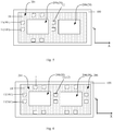
- first stitch marks 1' having a large annular shape as shown on the upper left part of Fig. 1 are formed on a planarization layer/pixel definition layer 10' on periphery of a display panel region 200' (each display panel region 200' is used to form one display substrate) of a substrate 100' by a shot using the stitch marks on an upper frame and a left frame of the mask, and second stitch marks 2' having a small square shape as shown on the lower left part of Fig.
- a specific principle of obtaining the offset between two shots is: as shown in Fig. 3 , on the planarization layer/pixel definition layer 10' between the two adjacent display panel regions 200', a former shot can give rise to the second stitch marks 2' having the small square shape (for example, 15 um) as shown in Fig. 3 , and a latter shot can give rise to the first stitch marks 1' having the large annular shape (for example, an inner diameter: 7.5 um, an outer diameter: 20 um) as shown in Fig. 3 .
- the small square shape corresponds to the large annular shape in position, a small annular shape (for example, an inner diameter: 7.5 um, an outer diameter: 15 um) is finally formed.
- the small-area island-like stitch marks (the annular shape, the small square shape) tend to peel off. After peeling off, the island-like stitch marks are washed by a washing liquid to a backplane circuit or a light-emitting pixel region, which impacts light emitting and product yield, as shown in Fig. 4 .
- a method for manufacturing a display substrate motherboard includes a substrate, the substrate includes at least two display panel regions, and a mark area is provided on periphery of each of the display panel regions.
- the method includes: forming a first film in the mark area of the substrate; and performing a patterning process on the first film to form a plurality of stitch marks.
- the plurality of stitch marks are via holes formed in the first film.
- the plurality of stitch marks of the display substrate motherboard manufactured by using the above method are via holes formed in the film, instead of the small area island-like film patterns, thereby eliminating a possibility of the stitch mark peeling off, and further ensuring a reliability and yield of the product.
- the display substrate motherboard manufactured by using the method as described above is further provided in the present disclosure
- the display substrate motherboard includes the first film in the mark area
- the first film includes a plurality of stitch marks on the substrate
- the stitch marks are via holes formed in the first film.
- the same functional film pattern includes pixel electrodes, gate electrodes, source electrodes, or drain electrodes of thin film transistors of each display panel region.
- stitch marks are manufactured on periphery of the display panel regions, and the offset between two shots is obtained by using the stitch marks.
- the technical solution of the present disclosure is specifically introduced by taking a case in which one mask is used to expose the film of only one display panel region at a time for example. It is only exemplary, and the technical solution of the present disclosure is also applicable to the case where one mask is used to expose films of at least two adjacent display panel regions at a time. In this case, the at least two adjacent display panel regions may be regarded as a larger display panel region, the technical solution is the same as or similar to the technical solution in the case of exposing the film of only one display panel region at a time by using one mask, and a repeated description thereof is omitted.
- the two successive shots in this embodiment refers to two exposure processes of manufacturing the same functional film pattern in the two adjacent display panel regions.
- performing a patterning process on the display panel region refers to performing the patterning process on the film in the display panel region.
- the patterning process includes an exposure process performed on the film in the display panel region by using a mask.
- the display substrate motherboard in the embodiment includes a substrate 100.
- the substrate 100 includes at least two display panel regions 200.
- a mark area 201 is provided on periphery of each of the display panel regions 200.
- the method for manufacturing the display substrate motherboard in the embodiment includes: forming a first film 10 in the mark area 201, and performing a patterning process on the first film 10 to form a plurality of stitch marks, the plurality of stitch marks are via holes 101 formed in the first film 10; forming a second film 20 in each of the display panel regions 200 and performing a patterning process on the second film 20 to form a pattern of the second film 20.
- the forming the first film 10 in the mark area 201 and forming the second film 20 in the display panel region 200 includes: forming the first film 10 and the second film 20 simultaneously in one film forming process by using a same material.
- the first film 10 and the second film 20 are a same film, so as to simplify the manufacturing process and reduce costs.
- first film 10 and the second film 20 are made of a photoresist, and the via holes 101 (stitch marks) in the first film 10 and the pattern of the second film 20 may be formed by only using an exposure process, which further simplifies the manufacturing process.
- the performing the patterning process on the first film 10 and performing the patterning process on the second film 20 includes: sequentially patterning second films 20 in all the display panel regions 200 and first films 10 in corresponding mark areas 201 by using a mask, where the second film 20 in each of the display panel regions 200 and the first film 10 in the corresponding mark area 201 are patterned simultaneously in one patterning process by using the mask, to form the pattern of the second film 20 and the plurality of stitch marks on the first film 10.
- the stitch marks formed in the above steps includes: at least one first stitch mark 11 on one side of the display panel region 200 and at least one second stitch mark 12 on the opposite side of the display panel region 200, the first stitch mark 11 and the second stitch mark 12 are provided between two adjacent display panel regions 200, so as to obtain an exposure offset between patterning processes performed on the second films of two adjacent display panel regions 200 according to an offset relative to a set distance between the first stitch mark 11 and the second stitch mark 12 corresponding in position and located between the two adjacent display panel regions 200.
- the exposure offset between patterning processes of two adjacent display panel regions is obtained by using the stitch marks corresponding in position and located between the two adjacent display panel regions according to the above method, since the stitch marks are the via holes in the film, instead of the small area island-like film patterns, a possibility of the stitch mark peeling off is eliminated, and the reliability and the yield of the product is further ensured.
- a process of obtaining the exposure offset of a process of manufacturing the display substrate motherboard includes: obtaining the exposure offset between patterning processes performed on the second films of two adjacent display panel regions according to the offset relative to the set distance between the first stitch mark and the second stitch mark corresponding in position and located in the mark area between the two adjacent display panel regions.
- a specific principle of obtaining the offset between two successive exposure processes of two adjacent display panel regions 200 is: since the display panel region 200 and the stitch marks on periphery of the display panel region 200 are manufactured by using the same mask, the exposure offset between patterning processes of the two adjacent display panel regions 200 is equal to the exposure offset between patterning processes of forming the stitch marks corresponding in position and on periphery of the two adjacent display panel regions 200. Therefore, the exposure offset between patterning processes performed on the second films 20 of two adjacent display panel regions 200 can be obtained by using the offset (i.e., the exposure offset) relative to a set distance between the stitch marks corresponding in position and on periphery of the two adjacent display panel regions 200.
- the stitch marks on periphery of all the display panel regions 200 are manufactured by using the same mask, the stitch marks are distributed on periphery of all the display panel regions 200 according to the same rule, and a set distance between the first stitch mark 11 and the second stitch mark 12 located between two adjacent display panel regions 200 may be set by setting a distance between the two adjacent display panel regions 200.
- a set distance between the first stitch mark 11 and the second stitch mark 12 located between two adjacent display panel regions 200 may be set by setting a distance between the two adjacent display panel regions 200.
- the exposure offset between patterning processes performed on the second films 20 of two adjacent display panel regions 200 may be obtained according to the offset (i.e., the exposure offset) relative to the set distance between the first stitch mark 11 and the second stitch mark 12 corresponding in position and located between the two adjacent display panel regions 200.
- the exposure offset between patterning processes performed on the second films of two adjacent display panel regions is obtained according to the offset relative to the set distance between the stitch marks corresponding in position and located between the two adjacent display panel regions, since the distance is relatively small, the exposure offset between the two adjacent display panel regions can be obtained quickly and accurately.
- the first stitch mark 11 and the second stitch mark 12 provided on opposite sides of a same display panel region 200 have a one-to-one correspondence in position.
- a plurality of stitch marks are provided on one side of the display panel region 200, there are multiple groups of the first stitch mark 11 and the second stitch mark 12 corresponding in position and located between two adjacent display panel regions 200.
- the accuracy of the obtained exposure offset between the patterning processes of the two adjacent display panel regions 200 can be improved by measuring the offsets relative to the set distances of the multiple groups of the first stitch mark 11 and the second stitch mark 12 corresponding in position.
- a position correspondence between a first stitch mark 11 on one side of the display panel region 200 and two second stitch marks 12 on the opposite side of the display panel region 200 may be set.
- two offsets relative to set distances can be obtained from one group of the first stitch mark 11 and the second stitch marks 12 corresponding in position, thereby further improving the accuracy of the obtained exposure offset between the patterning processes of the two adjacent display panel regions 200.
- first stitch mark and the second stitch mark corresponding in position and located between two adjacent display panel regions is not limited to the above two types.
- a position correspondence between one first stitch mark and three second stitch marks may be set, or set distances between a center of one first stitch mark and centers of multiple second stitch marks corresponding in position and located between two adjacent display panel regions are zero, which is not enumerated one by one herein, and falls within the scope of the embodiments of the present disclosure.
- the stitch mark can be a via hole 101 having a regular shape, such as a rectangular hole as shown in Figs. 7 and 9 , a cross-shaped hole as shown in Fig. 10 , a triangular hole as shown in Fig. 11 .
- the stitch mark can also be via holes 101 having other regular shapes, which are not enumerated herein one by one.
- the stitch mark can also be a via hole 101 having an irregular shape.
- the stitch mark is provided as the via hole 101 having a regular shape, to facilitate obtaining the offset relative to the set distance between the first stitch mark 11 and the second stitch mark 12 corresponding in position and located between the two adjacent display panel regions 200.
- shapes and sizes of all the stitch marks provided on periphery of the display panel region 200 are the same. According to same reference points on the outlines of the stitch marks, the offset between two stitch marks corresponding in position and located between two adjacent display panel regions 200 may be obtained, to further facilitate the acquisition of the offset relative to the set distance between the two stitch marks, as shown in Fig. 7 and Fig. 8 .
- the set distance between the first stitch mark and the second stitch mark corresponding in position and located between two adjacent display panel regions can be arbitrarily set as required, and can be a value larger than zero (when there is no exposure offset, the first stitch mark 11 and the second stitch mark 12 corresponding in position and located between two adjacent display panel regions are spaced), can also be a value smaller than zero (when there is no exposure offset, the first stitch mark 11 and the second stitch mark 12 corresponding in position and located between two adjacent display panel regions overlap partially), or can be equal to zero (when there is no exposure offset, the centers of the first stitch mark 11 and the second stitch mark 12 corresponding in position and located between two adjacent display panel regions 200 coincide with each other, as shown in Fig. 6 ).
- the set distance is set to zero, and thus it is easier to obtain the offset relative to the set distance between the first stitch mark 11 and the second stitch mark 12 corresponding in position and located between two adjacent display panel regions 200.
- the shapes and the sizes of all the stitch marks provided on periphery of the display panel region 200 are the same, and the set distance is zero.
- a distance between same reference points on the outlines of the first stitch mark 11 and the second stitch mark 12 corresponding in position and located between two adjacent display panel regions 200 i.e., the offset relative to the set distance.
- all the stitch marks on periphery of the display panel region 200 are square holes of the same size, a distance between vertices at the same position (for example, upper right vertices as shown in Fig. 7 ) of the first stitch mark 11 and the second stitch mark 12 corresponding in position and located between two adjacent display panel regions 200 is the offset relative to the set distance.
- the first stitch mark 11 and the second stitch mark 12 provided on periphery of the display panel region 200 have a one-to-one correspondence in position, and a first connection line of centers of the first stitch mark 11 and the second stitch mark 12 corresponding in position extends along a first direction, e.g., an X direction as shown in Fig. 7 .
- the substrate 100 includes two display panel regions 200 adjacent in the first direction, a second connection line of centers of the two display panel regions 200 is parallel to the first connection line (i.e., the two adjacent display panel regions 200 are arranged along the first direction), a distance between the centers of the two display panel regions 200 is equal to a distance between centers of the first stitch mark 11 and the second stitch mark 12 corresponding in position and on opposite sides of a display panel region 200, and the set distance is zero. That is, when there is no exposure offset, the first stitch mark 11 and the second stitch mark 12 corresponding in position and located between the two adjacent display panel regions 200 coincide with each other, as shown in Fig. 6 .
- the first stitch mark 11 and the second stitch mark 12 corresponding in position and located between two adjacent display panel regions do not coincide with each other anymore, and are offset from each.
- the exposure offset between patterning processes of the two display panel regions 200 may be obtained based on a first offset x in the first direction (the X direction as shown in Fig.
- an offset in the first direction is x
- an offset in the second direction perpendicular to the first direction is y.
- all the stitch marks on periphery of the display panel region 200 are of regular shapes with the same shape and size, which facilitates the acquisition of the offset relative to the set distance between the first stitch mark 11 and the second stitch mark 12 corresponding in position and located between two adjacent display panel regions 200.
- the exposure offset between patterning processes of the two display panel regions 200 may be obtained by obtaining the offset relative to the set distance between the vertices at the upper right corners of the first stitch mark 11 and the second stitch mark 12 corresponding in position and located between two adjacent display panel regions 200, and the exposure offset can be broken down into the offset x in the first direction and the offset y in the second direction perpendicular to the first direction.
- the first stitch mark and the second stitch mark on opposite sides of a display panel region and corresponding in position can be, but are not limited to, substantially symmetrically distributed with respect to a central axis of the display panel region that is perpendicular to the first connection line.
- a plurality of groups of the first stitch mark and the second stitch mark having a one-to-one correspondence in position can be formed between two adjacent display panel regions, to facilitate the acquisition of the offset relative to the set distance between the first stitch mark and the second stitch mark corresponding in position.
- the accuracy can be improved by providing the plurality of groups of the first stitch mark and the second stitch mark having a one-to-one correspondence in position.
- two adjacent display panel regions are arranged along the first direction.
- the corresponding technical solutions are the same as above specific implementation.
- the substrate includes at least four display panel regions distributed in a substantially matrix along the first direction and the second direction, the corresponding technical solutions are a combination of the above two cases, which is not described in detail herein.
- the first film 10 used for manufacturing the stitch marks and the second film 20 of the display panel region 200 can be a same film in the embodiment, and can be manufactured simultaneously in one film forming process by using a same material.
- the display panel region of the organic electroluminescence display substrate motherboard includes various functional film layers of an organic electroluminescent diode, a pixel definition layer, a planarization layer, etc.
- the second film 20 in the embodiment can be the planarization layer or the pixel definition layer of the organic electroluminescence display substrate motherboard.
- the first film 10 used for manufacturing the stitch marks and the planarization layer or the pixel definition layer can be manufactured simultaneously in one film forming process by using a same material. Since the planarization layer are the pixel definition layer are thick, a planar surface can be provided, so that open ends of the via holes 101 are located in a same plane, which is beneficial to accurately obtain the exposure offset.
- the display panel region of the liquid crystal display substrate motherboard includes various functional film layers of a thin film transistor, a planarization layer, a pixel electrode, etc.
- the second film 20 in the embodiment may be the planarization layer of the liquid crystal display substrate motherboard.
- the first film 10 used for manufacturing the stitch marks and the planarization layer may be manufactured simultaneously in one film forming process by using a same material. Since the planarization layer is thick, a planar surface can be provided, so that open ends of the via holes 101 are located in a same plane, which is beneficial to accurately obtain the exposure offset.
- a method for manufacturing stitch marks of the display substrate motherboard specifically includes the following steps.
- a planarization layer 10 is deposited on the substrate 100.
- the planarization layer 10 is made of a positive photoresist.
- One display panel region 200 and the planarization layer 10 of a mark area on periphery of the display panel region 200 are simultaneously exposed in one patterning process by using a mask, and then developed to form the first stitch marks 11 and the second stitch marks 12 on opposite sides of the display panel region 200 on the planarization layer 10 of the mark area.
- the first stitch marks 11 and the second stitch marks 12 are via holes 101 in the planarization layer 10, as shown in Fig. 5 .
- Another display panel region 200 and the planarization layer 10 of a mark area on periphery of the display panel region 200 are simultaneously exposed in one patterning process by using the same mask, and then developed to form the first stitch marks 11 and the second stitch marks 12 on opposite sides of the display panel region 200 on the planarization layer 10 of the mark area, as shown in Fig. 7 .
- There is an offset between the exposures of the two adjacent display panel regions 200 thus there is an offset relative to a set distance between the first stitch mark 11 and the second stitch mark 12 corresponding in position and located between the two adjacent display panel regions 200, the set distance is zero.
- first stitch mark 11 and the second stitch mark 12 corresponding in position and located between two adjacent display panel regions coincide with each other, as shown in Fig. 6 .
- a first offset x 20 um in a first direction
- the stitch marks used to obtain the offset between two successive exposure processes of two adjacent display panel regions are taken as an example to specifically describe the technical solution of the present disclosure.
- the stitch marks in the embodiments of the present disclosure can also be alignment stitch marks, and alignment is performed on a mask and a display panel region by using the alignment stitch marks, to perform a patterning process on the display panel region.
- the performing the patterning process on the second film 20 to form the pattern of the second film 20 includes: when the second film 20 in at least one display panel region 200 of the substrate is to be patterned, performing alignment on the mask and the display panel region 200 by using the stitch marks 11 and 12, and patterning the second film 20 by using the mask.
- stitch marks of the present disclosure may also be stitch marks having other functions.
Landscapes
- Physics & Mathematics (AREA)
- Nonlinear Science (AREA)
- Mathematical Physics (AREA)
- Chemical & Material Sciences (AREA)
- Crystallography & Structural Chemistry (AREA)
- General Physics & Mathematics (AREA)
- Optics & Photonics (AREA)
- Spectroscopy & Molecular Physics (AREA)
- Electroluminescent Light Sources (AREA)
- Devices For Indicating Variable Information By Combining Individual Elements (AREA)
- Liquid Crystal (AREA)
Abstract
Description
- This application claims a priority to
Chinese Patent Application No. 201811279971.9 - The present disclosure relates to the field of display technology, in particular to a display substrate motherboard and a method for manufacturing the same.
- In a display substrate production line, a plurality of display substrates are manufactured on one display substrate motherboard, that is, a plurality of display panel regions are included on one substrate, and each display panel region is provided with all functional film patterns of a display substrate. After all the display substrates are manufactured, the display substrate motherboard is sliced into multiple independent display substrates by using a slicing process. During the manufacturing process performed on the display substrate motherboard, some stitch marks need to be manufactured on periphery of the display panel region for purposes such as alignment and obtaining an exposure offset. A conventional stitch mark is a film pattern having a small area, which is extremely easy to peel off, and is washed to the display panel region of the substrate, thereby affecting performance of a product, and even causing the product to malfunction.
- In a first aspect, a method for manufacturing a display substrate motherboard is provided in an embodiment of the present disclosure. The display substrate motherboard includes a substrate, the substrate includes at least two display panel regions, and a mark area is provided on periphery of each of the display panel regions. The method includes: forming a first film in the mark area; and performing a patterning process on the first film to form a plurality of stitch marks. The plurality of stitch marks are via holes formed in the first film.
- According to some possible embodiments of the present disclosure, the method further includes: forming a second film in each of the display panel regions of the substrate; and performing a patterning process on the second film to form a pattern of the second film, where the forming the first film in the mark area and forming the second film in each of the display panel regions of the substrate includes: forming the first film and the second film simultaneously in one film forming process by using a same material.
- According to some possible embodiments of the present disclosure, the performing the patterning process on the first film and the second film includes: sequentially patterning second films in all the display panel regions and first films in corresponding mark areas by using a mask, where the second film in each of the display panel regions and the first film in the corresponding mark area are patterned simultaneously in one patterning process by using the mask, to form the pattern of the second film and the plurality of stitch marks on the first film; where the plurality of formed stitch marks include: at least one first stitch mark on one side of the display panel region and at least one second stitch mark on an opposite side of the display panel region, a mark area between two adjacent display panel regions is provided with the first stitch mark and the second stitch mark, so as to obtain an exposure offset between patterning processes performed on the second films of the two adjacent display panel regions based on an offset relative to a set distance between the first stitch mark and the second stitch mark corresponding in position and in the mark area between the two adjacent display panel regions.
- According to some possible embodiments of the present disclosure, the display substrate motherboard is an organic electroluminescence display substrate motherboard; the performing the patterning process on the second film to form the pattern of the second film includes: patterning the second film to form a planarization layer or a pixel definition layer of the organic electroluminescence display substrate motherboard.
- According to some possible embodiments of the present disclosure, the display substrate motherboard is a liquid crystal display substrate motherboard; the performing the patterning process on the second film to form the pattern of the second film includes: patterning the second film to form a planarization layer of the liquid crystal display substrate mother board.
- According to some possible embodiments of the present disclosure, the first film and the second film are made of a photoresist.
- According to some possible embodiments of the present disclosure, the performing the patterning process on the second film to form the pattern of the second film includes: when the second film in at least one display panel region of the substrate is to be patterned, aligning a mask with the display panel region by using the stitch marks, and patterning the second film by using the mask.
- In a second aspect, a display substrate motherboard is provided in an embodiment of the present disclosure, including: a substrate including at least two display panel regions, where a mark area is provided on periphery of each of the display panel regions; and a first film in the mark area, where the first film includes a plurality of stitch marks, and the plurality of stitch marks are via holes formed in the first film.
- According to some possible embodiments of the present disclosure, the display substrate motherboard further includes: a second film disposed on the substrate, where the second film is in each of the display panel regions.
- According to some possible embodiments of the present disclosure, the first film and the second film are a same film.
- According to some possible embodiments of the present disclosure, the plurality of stitch marks includes at least one first stitch mark on one side of each of the display panel regions and at least one second stitch mark on the opposite side of each of the display panel regions, the first stitch mark and the second stitch mark are provided between two adjacent display panel regions, so as to obtain an exposure offset between patterning processes performed on the second films of the two adjacent display panel regions according to an offset relative to a set distance between the first stitch mark and the second stitch mark corresponding in position and between the two adjacent display panel regions.
- According to some possible embodiments of the present disclosure, orthographic projection lines, on one side of the substrate, of the first stitch mark and the second stitch mark corresponding in position on periphery of the display panel regions at least partially overlap, and a first connection line of centers of the first stitch mark and the second stitch mark corresponding in position extends substantially along a first direction; and the substrate includes two display panel regions adjacent in the first direction, a second connection line of centers of the two display panel regions is parallel to the first connection line, a distance between the centers of the two display panel regions is substantially equal to a distance between centers of the first stitch mark and the second stitch mark corresponding in position and on opposite sides of a display panel region, and the set distance is zero.
- According to some possible embodiments of the present disclosure, the first stitch mark and the second stitch mark corresponding in position and on opposite sides of one display panel region are substantially symmetrically distributed with respect to a central axis of the display panel region that is perpendicular to the first connection line.
- According to some possible embodiments of the present disclosure, a shape and an aperture size of the first stitch mark are substantially the same as a shape and an aperture size of the second stitch mark.
- According to some possible embodiments of the present disclosure, the substrate includes at least four display panel regions, and the at least four display panel regions are distributed substantially in matrix.
- According to some possible embodiments of the present disclosure, the display substrate motherboard is an organic electroluminescence display substrate motherboard; and the second film is a planarization layer or a pixel definition layer of the organic electroluminescence display substrate motherboard.
- According to some possible embodiments of the present disclosure, the display substrate motherboard is a liquid crystal display substrate motherboard; and the second film is a planarization layer of the liquid crystal display substrate motherboard.
- According to some possible embodiments of the present disclosure, the stitch marks are regular-shaped via holes.
- According to some possible embodiments of the present disclosure, the via hole includes at least one of a rectangular hole, a cross-shaped hole, or a triangular hole.
- According to some possible embodiments of the present disclosure, the stitch marks are irregular-shaped via holes.
- In a third aspect, a method for obtaining the exposure offset in a process of manufacturing the display substrate motherboard as described in the first aspect is provided in an embodiment of the present disclosure, including: obtaining the exposure offset between patterning processes performed on the second films of the two adjacent display panel regions according to the offset relative to the set distance between the first stitch mark and the second stitch mark corresponding in position and in the mark area between the two adjacent display panel regions.
- In order to illustrate the technical solutions of the embodiments of the present disclosure or in the related art in a clearer manner, the drawings desired for the descriptions of the present disclosure will be introduced hereinafter briefly. Obviously, the following drawings merely relate to some embodiments of the present disclosure, and based on these drawings, a person skilled in the art may obtain other drawings without any creative effort.
-
Fig. 1 and Fig. 2 show a process for manufacturing, on a substrate, stitch marks for obtaining an exposure offset between two adjacent display panel regions in the related art; -
Fig. 3 shows a principle of forming the stitch marks between the two adjacent display panel regions inFig. 2 ; -
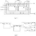
Fig. 4 is a schematic diagram illustrating that the stitch marks for obtaining the exposure offset between the two adjacent display panel regions on the substrate in the related art peel off; -
Fig. 5 andFig. 7 show a process for manufacturing, on a substrate, stitch marks for obtaining an exposure offset between two adjacent display panel regions according to embodiments of the present disclosure; -
Fig. 6 is a schematic diagram illustrating a substrate structure when there is no exposure offset between two adjacent display panel regions according to embodiments of the present disclosure; -
Fig. 8 shows a principle of forming the stitch marks between the two adjacent display panel regions inFig. 7 ; and -
Fig. 9 to Fig. 12 are schematic diagrams illustrating different substrate structures according to embodiments of the present disclosure. - In a display substrate production line, a plurality of display substrates are manufactured on one display substrate motherboard, that is, a plurality of display panel regions are included on one substrate, and each display panel region is provided with all functional film patterns of the display substrate. After all the display substrates are manufactured, they are sliced into a plurality of independent display substrates by using a slicing process. During a process for manufacturing the display substrate motherboard, some stitch marks need to be manufactured on periphery of the display panel region for purposes such as alignment and obtaining an exposure offset. A stitch mark in the related art is a film pattern having a small area, and the stitch mark can be of a cross shape, an annular shape, a square shape, or the like. The stitch mark having the small area is extremely easy to peel off, and is washed to the display panel region of the substrate, which affects performance of a product, and even causes the product to malfunction.
- Specifically, in a production process of a small-sized display substrate, a plurality of display substrates are manufactured on one substrate, and after the manufacture is completed, the substrate is sliced into multiple independent display substrates by using a slicing process. Since a size of a mask is smaller than that of the substrate, multiple exposures are required for one substrate. Each exposure with the mask is called a shot. Stitch marks are used to determine the exposure offset between two shots on a same substrate. A distribution of the stitch marks on the substrate/mask and an exposure relationship between shots are described as follows.
- Six groups of stitch marks are distributed on periphery of the mask. As shown in
Fig. 1 and Fig. 2 , first stitch marks 1' having a large annular shape as shown on the upper left part ofFig. 1 are formed on a planarization layer/pixel definition layer 10' on periphery of a display panel region 200' (each display panel region 200' is used to form one display substrate) of a substrate 100' by a shot using the stitch marks on an upper frame and a left frame of the mask, and second stitch marks 2' having a small square shape as shown on the lower left part ofFig. 1 are formed on the planarization layer/pixel definition layer 10' on periphery of the display panel region 200' of the substrate 100' by a shot using the stitch marks on a lower frame and a right frame of the mask. The two shots overlap, such that a first stitch mark 1' and a second stitch mark 2' corresponding in position and located between two adjacent display panel regions 200' are combined into a third stitch mark 3' having a small annular shape, as shown inFig. 3 . - A specific principle of obtaining the offset between two shots is: as shown in
Fig. 3 , on the planarization layer/pixel definition layer 10' between the two adjacent display panel regions 200', a former shot can give rise to the second stitch marks 2' having the small square shape (for example, 15 um) as shown inFig. 3 , and a latter shot can give rise to the first stitch marks 1' having the large annular shape (for example, an inner diameter: 7.5 um, an outer diameter: 20 um) as shown inFig. 3 . When the small square shape corresponds to the large annular shape in position, a small annular shape (for example, an inner diameter: 7.5 um, an outer diameter: 15 um) is finally formed. The offset between the two shots may be determined by measuring a horizontal aperture size d' of the small annular shape. When the offset between the two shots is zero, d = 15-7.5 = 7.5 um. - However, due to material of the planarization layer/pixel definition layer, the small-area island-like stitch marks (the annular shape, the small square shape) tend to peel off. After peeling off, the island-like stitch marks are washed by a washing liquid to a backplane circuit or a light-emitting pixel region, which impacts light emitting and product yield, as shown in
Fig. 4 . - In order to solve the above technical problems, a method for manufacturing a display substrate motherboard is provided, the display substrate motherboard includes a substrate, the substrate includes at least two display panel regions, and a mark area is provided on periphery of each of the display panel regions. The method includes: forming a first film in the mark area of the substrate; and performing a patterning process on the first film to form a plurality of stitch marks. The plurality of stitch marks are via holes formed in the first film.
- The plurality of stitch marks of the display substrate motherboard manufactured by using the above method are via holes formed in the film, instead of the small area island-like film patterns, thereby eliminating a possibility of the stitch mark peeling off, and further ensuring a reliability and yield of the product.
- Correspondingly, a display substrate motherboard manufactured by using the method as described above is further provided in the present disclosure, the display substrate motherboard includes the first film in the mark area, the first film includes a plurality of stitch marks on the substrate, and the stitch marks are via holes formed in the first film.
- Specific implementations of the present disclosure will be described in further detail below with reference to the drawings and embodiments. The following embodiments are used to illustrate the present disclosure, but not to limit the scope of the present disclosure.
- Due to a large size of the display substrate motherboard, and a relatively small size, which is limited by exposure accuracy and cost, of the mask used for exposing the film on the display substrate motherboard, multiple exposure processes using a mask are required to be performed to complete the manufacture of the same function film pattern on multiple display panel regions of a display substrate motherboard. Taking a liquid crystal display substrate motherboard as an example, the same functional film pattern includes pixel electrodes, gate electrodes, source electrodes, or drain electrodes of thin film transistors of each display panel region.
- In order to obtain an offset between two successive shots on two adjacent display panel regions, stitch marks are manufactured on periphery of the display panel regions, and the offset between two shots is obtained by using the stitch marks.
- In this embodiment, the technical solution of the present disclosure is specifically introduced by taking a case in which one mask is used to expose the film of only one display panel region at a time for example. It is only exemplary, and the technical solution of the present disclosure is also applicable to the case where one mask is used to expose films of at least two adjacent display panel regions at a time. In this case, the at least two adjacent display panel regions may be regarded as a larger display panel region, the technical solution is the same as or similar to the technical solution in the case of exposing the film of only one display panel region at a time by using one mask, and a repeated description thereof is omitted.
- It should be noted that the two successive shots in this embodiment refers to two exposure processes of manufacturing the same functional film pattern in the two adjacent display panel regions.
- In the following, performing a patterning process on the display panel region refers to performing the patterning process on the film in the display panel region. The patterning process includes an exposure process performed on the film in the display panel region by using a mask.
- As shown in
Fig. 5 andFig. 7 , the display substrate motherboard in the embodiment includes asubstrate 100. Thesubstrate 100 includes at least twodisplay panel regions 200. Amark area 201 is provided on periphery of each of thedisplay panel regions 200. - The method for manufacturing the display substrate motherboard in the embodiment includes: forming a
first film 10 in themark area 201, and performing a patterning process on thefirst film 10 to form a plurality of stitch marks, the plurality of stitch marks are viaholes 101 formed in thefirst film 10; forming asecond film 20 in each of thedisplay panel regions 200 and performing a patterning process on thesecond film 20 to form a pattern of thesecond film 20. - The forming the
first film 10 in themark area 201 and forming thesecond film 20 in thedisplay panel region 200 includes: forming thefirst film 10 and thesecond film 20 simultaneously in one film forming process by using a same material. - That is, the
first film 10 and thesecond film 20 are a same film, so as to simplify the manufacturing process and reduce costs. - Further, the
first film 10 and thesecond film 20 are made of a photoresist, and the via holes 101 (stitch marks) in thefirst film 10 and the pattern of thesecond film 20 may be formed by only using an exposure process, which further simplifies the manufacturing process. - The performing the patterning process on the
first film 10 and performing the patterning process on thesecond film 20 includes: sequentially patterningsecond films 20 in all thedisplay panel regions 200 andfirst films 10 in correspondingmark areas 201 by using a mask, where thesecond film 20 in each of thedisplay panel regions 200 and thefirst film 10 in thecorresponding mark area 201 are patterned simultaneously in one patterning process by using the mask, to form the pattern of thesecond film 20 and the plurality of stitch marks on thefirst film 10. - The stitch marks formed in the above steps includes: at least one
first stitch mark 11 on one side of thedisplay panel region 200 and at least onesecond stitch mark 12 on the opposite side of thedisplay panel region 200, thefirst stitch mark 11 and thesecond stitch mark 12 are provided between two adjacentdisplay panel regions 200, so as to obtain an exposure offset between patterning processes performed on the second films of two adjacentdisplay panel regions 200 according to an offset relative to a set distance between thefirst stitch mark 11 and thesecond stitch mark 12 corresponding in position and located between the two adjacentdisplay panel regions 200. - The exposure offset between patterning processes of two adjacent display panel regions is obtained by using the stitch marks corresponding in position and located between the two adjacent display panel regions according to the above method, since the stitch marks are the via holes in the film, instead of the small area island-like film patterns, a possibility of the stitch mark peeling off is eliminated, and the reliability and the yield of the product is further ensured.
- In this embodiment, a process of obtaining the exposure offset of a process of manufacturing the display substrate motherboard includes: obtaining the exposure offset between patterning processes performed on the second films of two adjacent display panel regions according to the offset relative to the set distance between the first stitch mark and the second stitch mark corresponding in position and located in the mark area between the two adjacent display panel regions.
- In the technical solutions provided in the embodiments of the present disclosure, a specific principle of obtaining the offset between two successive exposure processes of two adjacent
display panel regions 200 is: since thedisplay panel region 200 and the stitch marks on periphery of thedisplay panel region 200 are manufactured by using the same mask, the exposure offset between patterning processes of the two adjacentdisplay panel regions 200 is equal to the exposure offset between patterning processes of forming the stitch marks corresponding in position and on periphery of the two adjacentdisplay panel regions 200. Therefore, the exposure offset between patterning processes performed on thesecond films 20 of two adjacentdisplay panel regions 200 can be obtained by using the offset (i.e., the exposure offset) relative to a set distance between the stitch marks corresponding in position and on periphery of the two adjacentdisplay panel regions 200. - In addition, since the stitch marks on periphery of all the
display panel regions 200 are manufactured by using the same mask, the stitch marks are distributed on periphery of all thedisplay panel regions 200 according to the same rule, and a set distance between thefirst stitch mark 11 and thesecond stitch mark 12 located between two adjacentdisplay panel regions 200 may be set by setting a distance between the two adjacentdisplay panel regions 200. When there is an offset between the shots of two adjacentdisplay panel regions 200, there is also an offset in the stitch marks formed by the shots on periphery of the twodisplay panel regions 200. Therefore, the exposure offset between patterning processes performed on thesecond films 20 of two adjacentdisplay panel regions 200 may be obtained according to the offset (i.e., the exposure offset) relative to the set distance between thefirst stitch mark 11 and thesecond stitch mark 12 corresponding in position and located between the two adjacentdisplay panel regions 200. - Due to the fact that the exposure offset between patterning processes performed on the second films of two adjacent display panel regions is obtained according to the offset relative to the set distance between the stitch marks corresponding in position and located between the two adjacent display panel regions, since the distance is relatively small, the exposure offset between the two adjacent display panel regions can be obtained quickly and accurately.
- Optionally, as shown in
Fig. 7 , thefirst stitch mark 11 and thesecond stitch mark 12 provided on opposite sides of a samedisplay panel region 200 have a one-to-one correspondence in position. When a plurality of stitch marks are provided on one side of thedisplay panel region 200, there are multiple groups of thefirst stitch mark 11 and thesecond stitch mark 12 corresponding in position and located between two adjacentdisplay panel regions 200. The accuracy of the obtained exposure offset between the patterning processes of the two adjacentdisplay panel regions 200 can be improved by measuring the offsets relative to the set distances of the multiple groups of thefirst stitch mark 11 and thesecond stitch mark 12 corresponding in position. - As shown in
Fig. 12 , a position correspondence between afirst stitch mark 11 on one side of thedisplay panel region 200 and two second stitch marks 12 on the opposite side of thedisplay panel region 200 may be set. Thus, two offsets relative to set distances can be obtained from one group of thefirst stitch mark 11 and the second stitch marks 12 corresponding in position, thereby further improving the accuracy of the obtained exposure offset between the patterning processes of the two adjacentdisplay panel regions 200. - Of course, a combination relationship between the first stitch mark and the second stitch mark corresponding in position and located between two adjacent display panel regions is not limited to the above two types. For example, a position correspondence between one first stitch mark and three second stitch marks may be set, or set distances between a center of one first stitch mark and centers of multiple second stitch marks corresponding in position and located between two adjacent display panel regions are zero, which is not enumerated one by one herein, and falls within the scope of the embodiments of the present disclosure.
- The stitch mark can be a via
hole 101 having a regular shape, such as a rectangular hole as shown inFigs. 7 and9 , a cross-shaped hole as shown inFig. 10 , a triangular hole as shown inFig. 11 . Of course, the stitch mark can also be viaholes 101 having other regular shapes, which are not enumerated herein one by one. Or, the stitch mark can also be a viahole 101 having an irregular shape. - As an optional example, the stitch mark is provided as the via
hole 101 having a regular shape, to facilitate obtaining the offset relative to the set distance between thefirst stitch mark 11 and thesecond stitch mark 12 corresponding in position and located between the two adjacentdisplay panel regions 200. - Further, shapes and sizes of all the stitch marks provided on periphery of the
display panel region 200 are the same. According to same reference points on the outlines of the stitch marks, the offset between two stitch marks corresponding in position and located between two adjacentdisplay panel regions 200 may be obtained, to further facilitate the acquisition of the offset relative to the set distance between the two stitch marks, as shown inFig. 7 and Fig. 8 . - The set distance between the first stitch mark and the second stitch mark corresponding in position and located between two adjacent display panel regions can be arbitrarily set as required, and can be a value larger than zero (when there is no exposure offset, the
first stitch mark 11 and thesecond stitch mark 12 corresponding in position and located between two adjacent display panel regions are spaced), can also be a value smaller than zero (when there is no exposure offset, thefirst stitch mark 11 and thesecond stitch mark 12 corresponding in position and located between two adjacent display panel regions overlap partially), or can be equal to zero (when there is no exposure offset, the centers of thefirst stitch mark 11 and thesecond stitch mark 12 corresponding in position and located between two adjacentdisplay panel regions 200 coincide with each other, as shown inFig. 6 ). - In this embodiment, the set distance is set to zero, and thus it is easier to obtain the offset relative to the set distance between the
first stitch mark 11 and thesecond stitch mark 12 corresponding in position and located between two adjacentdisplay panel regions 200. - As an optional example, as shown in
Fig. 7 , the shapes and the sizes of all the stitch marks provided on periphery of thedisplay panel region 200 are the same, and the set distance is zero. According to the same reference points on the outlines of the stitch marks, a distance between same reference points on the outlines of thefirst stitch mark 11 and thesecond stitch mark 12 corresponding in position and located between two adjacentdisplay panel regions 200, i.e., the offset relative to the set distance, is obtained. For example, when all the stitch marks on periphery of thedisplay panel region 200 are square holes of the same size, a distance between vertices at the same position (for example, upper right vertices as shown inFig. 7 ) of thefirst stitch mark 11 and thesecond stitch mark 12 corresponding in position and located between two adjacentdisplay panel regions 200 is the offset relative to the set distance. - It should be noted that, the descriptions of the orientation in the embodiment, such as: left, right, up, or down, are defined in terms of the directions in the drawings, which are only for convenience of description, and are by no means limiting.
- In a specific implementation, as shown in
Fig. 5 andFig. 7 , thefirst stitch mark 11 and thesecond stitch mark 12 provided on periphery of thedisplay panel region 200 have a one-to-one correspondence in position, and a first connection line of centers of thefirst stitch mark 11 and thesecond stitch mark 12 corresponding in position extends along a first direction, e.g., an X direction as shown inFig. 7 . - The
substrate 100 includes twodisplay panel regions 200 adjacent in the first direction, a second connection line of centers of the twodisplay panel regions 200 is parallel to the first connection line (i.e., the two adjacentdisplay panel regions 200 are arranged along the first direction), a distance between the centers of the twodisplay panel regions 200 is equal to a distance between centers of thefirst stitch mark 11 and thesecond stitch mark 12 corresponding in position and on opposite sides of adisplay panel region 200, and the set distance is zero. That is, when there is no exposure offset, thefirst stitch mark 11 and thesecond stitch mark 12 corresponding in position and located between the two adjacentdisplay panel regions 200 coincide with each other, as shown inFig. 6 . - As shown in
Fig. 7 , in case that there is an exposure offset between patterning processes of the twodisplay panel regions 200, since an exposure process is performed on thedisplay panel region 200 and themark area 201 on periphery of thedisplay panel region 200 by using a same mask, there is also an exposure offset between patterning processes of forming the stitch marks on periphery of the two adjacentdisplay panel regions 200. That is to say, thefirst stitch mark 11 and thesecond stitch mark 12 corresponding in position and located between two adjacent display panel regions do not coincide with each other anymore, and are offset from each. The exposure offset between patterning processes of the twodisplay panel regions 200 may be obtained based on a first offset x in the first direction (the X direction as shown inFig. 7 ) and a second offset y in a second direction (a Y direction as shown inFig. 7 ) perpendicular to the first direction of thefirst stitch mark 11 and thesecond stitch mark 12. That is, an offset in the first direction is x, and an offset in the second direction perpendicular to the first direction is y. - In the embodiment, all the stitch marks on periphery of the
display panel region 200 are of regular shapes with the same shape and size, which facilitates the acquisition of the offset relative to the set distance between thefirst stitch mark 11 and thesecond stitch mark 12 corresponding in position and located between two adjacentdisplay panel regions 200. - As shown in
Fig. 7 , taking the case that the stitch mark is a square shaped hole for example, and setting a vertex at an upper right corner of the stitch mark as a reference point, the exposure offset between patterning processes of the twodisplay panel regions 200 may be obtained by obtaining the offset relative to the set distance between the vertices at the upper right corners of thefirst stitch mark 11 and thesecond stitch mark 12 corresponding in position and located between two adjacentdisplay panel regions 200, and the exposure offset can be broken down into the offset x in the first direction and the offset y in the second direction perpendicular to the first direction. - The first stitch mark and the second stitch mark on opposite sides of a display panel region and corresponding in position can be, but are not limited to, substantially symmetrically distributed with respect to a central axis of the display panel region that is perpendicular to the first connection line.
- In the above specific implementation, by providing the stitch marks located on opposite sides of the display panel region and corresponding in position one to one, a plurality of groups of the first stitch mark and the second stitch mark having a one-to-one correspondence in position can be formed between two adjacent display panel regions, to facilitate the acquisition of the offset relative to the set distance between the first stitch mark and the second stitch mark corresponding in position. Moreover, the accuracy can be improved by providing the plurality of groups of the first stitch mark and the second stitch mark having a one-to-one correspondence in position.
- In the above specific implementation, two adjacent display panel regions are arranged along the first direction. As for the case that two adjacent display panel regions are arranged along the second direction perpendicular to the first direction, the corresponding technical solutions are the same as above specific implementation. When the substrate includes at least four display panel regions distributed in a substantially matrix along the first direction and the second direction, the corresponding technical solutions are a combination of the above two cases, which is not described in detail herein.
- In order to simplify the manufacturing process, the
first film 10 used for manufacturing the stitch marks and thesecond film 20 of thedisplay panel region 200 can be a same film in the embodiment, and can be manufactured simultaneously in one film forming process by using a same material. - For example, when the display substrate motherboard in the embodiment is an organic electroluminescence display substrate motherboard, the display panel region of the organic electroluminescence display substrate motherboard includes various functional film layers of an organic electroluminescent diode, a pixel definition layer, a planarization layer, etc.
- The
second film 20 in the embodiment can be the planarization layer or the pixel definition layer of the organic electroluminescence display substrate motherboard. Thefirst film 10 used for manufacturing the stitch marks and the planarization layer or the pixel definition layer can be manufactured simultaneously in one film forming process by using a same material. Since the planarization layer are the pixel definition layer are thick, a planar surface can be provided, so that open ends of the via holes 101 are located in a same plane, which is beneficial to accurately obtain the exposure offset. - Similarly, when the display substrate motherboard in the embodiment is a liquid crystal display substrate motherboard, the display panel region of the liquid crystal display substrate motherboard includes various functional film layers of a thin film transistor, a planarization layer, a pixel electrode, etc.
- The
second film 20 in the embodiment may be the planarization layer of the liquid crystal display substrate motherboard. Thefirst film 10 used for manufacturing the stitch marks and the planarization layer may be manufactured simultaneously in one film forming process by using a same material. Since the planarization layer is thick, a planar surface can be provided, so that open ends of the via holes 101 are located in a same plane, which is beneficial to accurately obtain the exposure offset. - Taking the case that the display substrate motherboard is the organic electroluminescence display substrate motherboard for example, in this embodiment, a method for manufacturing stitch marks of the display substrate motherboard specifically includes the following steps.
- First, a
planarization layer 10 is deposited on thesubstrate 100. Theplanarization layer 10 is made of a positive photoresist. Onedisplay panel region 200 and theplanarization layer 10 of a mark area on periphery of thedisplay panel region 200 are simultaneously exposed in one patterning process by using a mask, and then developed to form the first stitch marks 11 and the second stitch marks 12 on opposite sides of thedisplay panel region 200 on theplanarization layer 10 of the mark area. The first stitch marks 11 and the second stitch marks 12 are viaholes 101 in theplanarization layer 10, as shown inFig. 5 . - Then, Another
display panel region 200 and theplanarization layer 10 of a mark area on periphery of thedisplay panel region 200 are simultaneously exposed in one patterning process by using the same mask, and then developed to form the first stitch marks 11 and the second stitch marks 12 on opposite sides of thedisplay panel region 200 on theplanarization layer 10 of the mark area, as shown inFig. 7 . There is an offset between the exposures of the two adjacentdisplay panel regions 200, thus there is an offset relative to a set distance between thefirst stitch mark 11 and thesecond stitch mark 12 corresponding in position and located between the two adjacentdisplay panel regions 200, the set distance is zero. Therefore, when there is no exposure offset, thefirst stitch mark 11 and thesecond stitch mark 12 corresponding in position and located between two adjacent display panel regions coincide with each other, as shown inFig. 6 . When there is an exposure offset, a first offset x = 20 um in a first direction and a second offset y = 20 um in a second direction perpendicular to the first direction between thefirst stitch mark 11 and thesecond stitch mark 12 corresponding in position and located between two adjacent display panel regions are the exposure offset between the two adjacentdisplay panel regions 200, as shown inFig. 8 . - At this point, the manufacture of the stitch marks is completed. As for the method for manufacturing other functional film layer patterns of the organic electroluminescence display substrate motherboard, a detailed description is omitted herein.
- In the above embodiments, the stitch marks used to obtain the offset between two successive exposure processes of two adjacent display panel regions are taken as an example to specifically describe the technical solution of the present disclosure.
- The stitch marks in the embodiments of the present disclosure can also be alignment stitch marks, and alignment is performed on a mask and a display panel region by using the alignment stitch marks, to perform a patterning process on the display panel region. Specifically, the performing the patterning process on the
second film 20 to form the pattern of thesecond film 20 includes: when thesecond film 20 in at least onedisplay panel region 200 of the substrate is to be patterned, performing alignment on the mask and thedisplay panel region 200 by using the stitch marks 11 and 12, and patterning thesecond film 20 by using the mask. - Of course, the stitch marks of the present disclosure may also be stitch marks having other functions.
- The above are merely some embodiments of the present disclosure, it should be noted that for those of ordinary skill in the art, various modifications and improvements may be made without departing from the principle of the present disclosure, and these modifications and improvements shall be deemed as falling within the scope of the present disclosure.
Claims (21)
- A method for manufacturing a display substrate motherboard comprising a substrate, the substrate comprising at least two display panel regions, and a mark area being provided on periphery of each of the display panel regions, the method comprising:forming a first film in the mark area; andperforming a patterning process on the first film to form a plurality of stitch marks,wherein the plurality of stitch marks are via holes formed in the first film.
- The method according to claim 1, further comprising:forming a second film in each of the display panel regions of the substrate; andperforming a patterning process on the second film to form a pattern of the second film,wherein the forming the first film in the mark area and the forming the second film in each of the display panel regions of the substrate comprises:
forming the first film and the second film simultaneously in one film forming process by using a same material. - The method according to claim 2, wherein the performing the patterning process on the first film and performing the patterning process on the second film comprise:sequentially patterning second films in all the display panel regions and first films in corresponding mark areas by using a mask, wherein the second film in each of the display panel regions and the first film in the corresponding mark area are patterned simultaneously in one patterning process by using the mask, to form the pattern of the second film and the plurality of stitch marks on the first film;wherein, the plurality of formed stitch marks comprise: at least one first stitch mark on one side of the display panel region and at least one second stitch mark on an opposite side of the display panel region, a mark area between two adjacent display panel regions is provided with the first stitch mark and the second stitch mark, so as to obtain an exposure offset between patterning processes performed on the second films of the two adjacent display panel regions based on an offset relative to a set distance between the first stitch mark and the second stitch mark corresponding in position and in the mark area between the two adjacent display panel regions.
- The method according to claim 2 or 3, wherein the display substrate motherboard is an organic electroluminescence display substrate motherboard;
the performing the patterning process on the second film to form the pattern of the second film comprises:
patterning the second film to form a planarization layer or a pixel definition layer of the organic electroluminescence display substrate motherboard. - The method according to claim 2 or 3, wherein the display substrate motherboard is a liquid crystal display substrate motherboard;
the performing the patterning process on the second film to form the pattern of the second film comprises:
patterning the second film to form a planarization layer of the liquid crystal display substrate mother board. - The method according to any one of claims 2 to 5, wherein the first film and the second film are made of a photoresist.
- The method according to any one of claims 2 to 6, wherein the performing the patterning process on the second film to form the pattern of the second film comprises:
when the second film in at least one display panel region of the substrate is to be patterned, aligning a mask with the display panel region by using the stitch marks, and patterning the second film by using the mask. - A display substrate motherboard, comprising:a substrate, comprising at least two display panel regions, wherein a mark area is provided on periphery of each of the display panel regions; anda first film in the mark area, wherein the first film comprises a plurality of stitch marks, and the plurality of stitch marks are via holes formed in the first film.
- The display substrate motherboard according to claim 8, further comprising:
a second film disposed on the substrate, wherein the second film is in each of the display panel regions. - The display substrate motherboard according to claim 9, wherein the first film and the second film are a same film.
- The display substrate motherboard according to claim 9 or 10, wherein the plurality of stitch marks comprise at least one first stitch mark on one side of each of the display panel regions and at least one second stitch mark on an opposite side of each of the display panel regions, the first stitch mark and the second stitch mark are provided between two adjacent display panel regions, so as to obtain an exposure offset between patterning processes performed on the second films of the two adjacent display panel regions based on an offset relative to a set distance between the first stitch mark and the second stitch mark corresponding in position and between the two adjacent display panel regions.
- The display substrate motherboard according to claim 11, wherein orthographic projection lines, on one side of the substrate, of the first stitch mark and the second stitch mark corresponding in position on periphery of the display panel region at least partially overlap, and a first connection line of centers of the first stitch mark and the second stitch mark corresponding in position extends substantially along a first direction; and
the substrate comprises two display panel regions adjacent in the first direction, a second connection line of centers of the two display panel regions is parallel to the first connection line, a distance between the centers of the two display panel regions is substantially equal to a distance between centers of the first stitch mark and the second stitch mark corresponding in position and on opposite sides of a display panel region, and the set distance is zero. - The display substrate motherboard according to claim 12, wherein the first stitch mark and the second stitch mark corresponding in position and on opposite sides of the display panel region are substantially symmetrically distributed with respect to a central axis of the display panel region that is perpendicular to the first connection line.
- The display substrate motherboard according to claim 13, wherein a shape and an aperture size of the first stitch mark are substantially the same as a shape and an aperture size of the second stitch mark.
- The display substrate motherboard according to claim 13, wherein the substrate comprises at least four display panel regions, and the at least four display panel regions are distributed substantially in matrix.
- The display substrate motherboard according to any one of claims 9 to 15, wherein the display substrate motherboard is an organic electroluminescence display substrate motherboard; and
the second film is a planarization layer or a pixel definition layer of the organic electroluminescence display substrate motherboard. - The display substrate motherboard according to any one of claims 9 to 15, wherein the display substrate motherboard is a liquid crystal display substrate motherboard; and
the second film is a planarization layer of the liquid crystal display substrate motherboard. - The display substrate motherboard according to any one of claims 8 to 17, wherein the stitch marks are regular-shaped via holes.
- The display substrate motherboard according to claim 18, wherein the via hole comprises at least one of a rectangular hole, a cross-shaped hole, or a triangular hole.
- The display substrate motherboard according to any one of claims 8 to 17, wherein the stitch marks are irregular-shaped via holes.
- A method for obtaining an exposure offset in a process of manufacturing the display substrate motherboard according to any one of claims 3 to 7, comprising:
obtaining the exposure offset between patterning processes performed on the second films of the two adjacent display panel regions based on the offset relative to the set distance between the first stitch mark and the second stitch mark corresponding in position and in the mark area between the two adjacent display panel regions.
Applications Claiming Priority (2)
| Application Number | Priority Date | Filing Date | Title |
|---|---|---|---|
| CN201811279971.9A CN111128963B (en) | 2018-10-30 | 2018-10-30 | Display substrate mother board and manufacturing method thereof |
| PCT/CN2019/103715 WO2020088082A1 (en) | 2018-10-30 | 2019-08-30 | Display substrate motherboard and manufacturing method therefor |
Publications (2)
| Publication Number | Publication Date |
|---|---|
| EP3876028A1 true EP3876028A1 (en) | 2021-09-08 |
| EP3876028A4 EP3876028A4 (en) | 2022-08-03 |
Family
ID=70463440
Family Applications (1)
| Application Number | Title | Priority Date | Filing Date |
|---|---|---|---|
| EP19856415.5A Pending EP3876028A4 (en) | 2018-10-30 | 2019-08-30 | DISPLAY SUBSTRATE MOTHERBOARD AND METHOD OF MAKING THEREOF |
Country Status (5)
| Country | Link |
|---|---|
| US (1) | US11227839B2 (en) |
| EP (1) | EP3876028A4 (en) |
| JP (1) | JP7793880B2 (en) |
| CN (1) | CN111128963B (en) |
| WO (1) | WO2020088082A1 (en) |
Families Citing this family (7)
| Publication number | Priority date | Publication date | Assignee | Title |
|---|---|---|---|---|
| CN111575648B (en) * | 2020-06-23 | 2022-07-15 | 京东方科技集团股份有限公司 | Mask assembly and method of making the same |
| CN111816685B (en) * | 2020-07-22 | 2022-12-13 | 京东方科技集团股份有限公司 | Display substrate, test method thereof and display device |
| CN114236969B (en) * | 2021-11-12 | 2024-08-02 | 京东方科技集团股份有限公司 | Exposure detection method and device |
| KR20230167792A (en) * | 2022-06-02 | 2023-12-12 | 삼성디스플레이 주식회사 | Exposure mask and method of manufacturing display device using the same |
| CN117311098A (en) * | 2022-06-17 | 2023-12-29 | 思特威(上海)电子科技股份有限公司 | Linear image sensor, manufacturing method and photolithography mask |
| CN115097667B (en) * | 2022-07-20 | 2023-10-17 | 京东方科技集团股份有限公司 | Display panel, manufacturing method thereof and display device |
| CN117935682B (en) * | 2024-01-29 | 2026-05-26 | 友达光电(厦门)有限公司 | Display panel motherboard and display panel |
Family Cites Families (25)
| Publication number | Priority date | Publication date | Assignee | Title |
|---|---|---|---|---|
| JPH116764A (en) * | 1997-04-23 | 1999-01-12 | Matsushita Electric Works Ltd | Infrared detector |
| KR20050060669A (en) * | 2003-12-17 | 2005-06-22 | 삼성전자주식회사 | Manufacturing method of thin film transistor array panel |
| TWI311369B (en) | 2006-03-24 | 2009-06-21 | Advanced Semiconductor Eng | Method for fabricating identification code on a substrate |
| KR20080061569A (en) * | 2006-12-28 | 2008-07-03 | 삼성전자주식회사 | Mother Display Panel for Display Panel Manufacturing |
| CN101726989B (en) * | 2009-11-16 | 2011-09-07 | 华映光电股份有限公司 | Method for manufacturing base plate with recognized mark |
| US9526167B2 (en) | 2010-11-02 | 2016-12-20 | Kyocera Corporation | Many-up wiring substrate, wiring board, and electronic device |
| CN102096328B (en) * | 2010-12-03 | 2012-11-21 | 深圳市华星光电技术有限公司 | Exposure procedure of liquid crystal panels and mask |
| JP5893967B2 (en) | 2011-06-28 | 2016-03-23 | 京セラ株式会社 | Multiple wiring board |
| CN103454852B (en) * | 2012-06-05 | 2016-07-13 | 中芯国际集成电路制造(上海)有限公司 | A kind of measuring method of mask plate and alignment precision |
| CN103605263B (en) * | 2013-09-17 | 2015-11-25 | 京东方科技集团股份有限公司 | A kind of method and mask plate detecting color membrane substrates splicing exposure error |
| CN103777364B (en) * | 2013-12-13 | 2017-10-13 | 北京维信诺科技有限公司 | A kind of manufacture method of graticle |
| KR102161586B1 (en) | 2013-12-30 | 2020-10-05 | 엘지디스플레이 주식회사 | Liquid crystal display panel and method of fabricating thereof |
| CN103995433B (en) * | 2014-05-14 | 2017-10-17 | 京东方科技集团股份有限公司 | Mask plate and base plate mark preparation method |
| CN204102865U (en) * | 2014-10-09 | 2015-01-14 | 中芯国际集成电路制造(北京)有限公司 | A kind of to locating tab assembly structure |
| CN104330912B (en) * | 2014-11-24 | 2017-12-26 | 京东方科技集团股份有限公司 | A kind of motherboard, to the motherboard after box, respective production method and liquid crystal display panel |
| CN104735912B (en) | 2015-03-10 | 2018-07-06 | 广州杰赛科技股份有限公司 | A kind of production method of stepped plate |
| CN104808451B (en) * | 2015-05-15 | 2017-07-18 | 合肥京东方光电科技有限公司 | A kind of contraposition exposure method |
| KR102411542B1 (en) * | 2015-05-19 | 2022-06-22 | 삼성디스플레이 주식회사 | Pattern forming method for pixel and pixel position accuracy inspection and the mask for the same |
| KR102544481B1 (en) * | 2016-04-25 | 2023-06-19 | 삼성디스플레이 주식회사 | Organic light emitting display panel and method of manufacturing an organic light emitting display panel |
| CN105957867B (en) | 2016-04-28 | 2018-12-18 | 京东方科技集团股份有限公司 | Array substrate motherboard and preparation method thereof, display device |
| CN105954985A (en) * | 2016-06-30 | 2016-09-21 | 上海华力微电子有限公司 | Method for measuring overlay precision of photoetching process, and mask plate |
| CN106647162B (en) * | 2017-03-22 | 2020-02-14 | 京东方科技集团股份有限公司 | Mask plate, exposure method and device |
| KR102322135B1 (en) * | 2017-09-15 | 2021-11-08 | 삼성디스플레이 주식회사 | Method for manufacturing of display device |
| CN207338364U (en) * | 2017-11-15 | 2018-05-08 | 京东方科技集团股份有限公司 | Display base plate, organic luminescent device and display device |
| KR102395221B1 (en) * | 2017-12-05 | 2022-05-10 | 삼성디스플레이 주식회사 | Display device |
-
2018
- 2018-10-30 CN CN201811279971.9A patent/CN111128963B/en active Active
-
2019
- 2019-08-30 WO PCT/CN2019/103715 patent/WO2020088082A1/en not_active Ceased
- 2019-08-30 EP EP19856415.5A patent/EP3876028A4/en active Pending
- 2019-08-30 JP JP2020564869A patent/JP7793880B2/en active Active
- 2019-08-30 US US16/649,787 patent/US11227839B2/en active Active
Also Published As
| Publication number | Publication date |
|---|---|
| WO2020088082A1 (en) | 2020-05-07 |
| CN111128963A (en) | 2020-05-08 |
| JP7793880B2 (en) | 2026-01-06 |
| US20210074649A1 (en) | 2021-03-11 |
| JP2022503370A (en) | 2022-01-12 |
| EP3876028A4 (en) | 2022-08-03 |
| US11227839B2 (en) | 2022-01-18 |
| CN111128963B (en) | 2022-04-26 |
Similar Documents
| Publication | Publication Date | Title |
|---|---|---|
| US11227839B2 (en) | Display substrate motherboard and method for manufacturing the same | |
| US10909901B2 (en) | Pixel arrangement, manufacturing method thereof, display panel, display device and mask | |
| CN102692831B (en) | Counterpoint mark and method for using same to manufacture workpieces in exposure process | |
| CN104317158B (en) | A kind of mask plate, mask plate group, color membrane substrates and display device | |
| TWI677089B (en) | Organic light-emitting display device, method of making the same, and mask for making support column | |
| US10866452B2 (en) | Color filter substrate, production method thereof, display panel, and display apparatus | |
| US10101661B2 (en) | Multi-layer substrate, preparation method thereof and display device | |
| US20240284726A1 (en) | Display panel and display device | |
| CN103904060B (en) | The design of TFT LCD array alignment mark and manufacture method | |
| WO2020253313A1 (en) | Display mother board, display panel, a spliced display screen, and display mother board manufacturing method | |
| US20150331310A1 (en) | Mask plate and a method for producing a substrate mark | |
| US20200201092A1 (en) | Array substrate and manufacturing method thereof and display panel | |
| WO2014127586A1 (en) | Dual visual field display substrate and display device | |
| US11864418B2 (en) | Display panel, preparation method thereof and display device | |
| CN104282623B (en) | OLED backboard and preparation method thereof, alignment system and alignment method thereof | |
| US11158799B2 (en) | Mask assembly and method of patterning semiconductor film using thereof | |
| CN119947425A (en) | Display motherboard and preparation method thereof, preparation method of display panel and display device | |
| CN108183123B (en) | Organic light emitting display panel and manufacturing method thereof | |
| CN104900572B (en) | The preparation method of alignment mark on grid layer | |
| CN116056499B (en) | Display panel and preparation method thereof | |
| EP3945610B1 (en) | Black matrix and method for manufacturing the same, and color filter substrate and method for manufacturing the same | |
| CN110233146B (en) | Element substrate and manufacturing method thereof | |
| CN115101704A (en) | Bonding apparatus and bonding method | |
| CN107748460B (en) | Substrate structure and manufacturing method thereof | |
| CN117706862A (en) | Mask plate, array substrate, preparation method of array substrate, display panel and display device |
Legal Events
| Date | Code | Title | Description |
|---|---|---|---|
| STAA | Information on the status of an ep patent application or granted ep patent |
Free format text: STATUS: UNKNOWN |
|
| STAA | Information on the status of an ep patent application or granted ep patent |
Free format text: STATUS: THE INTERNATIONAL PUBLICATION HAS BEEN MADE |
|
| PUAI | Public reference made under article 153(3) epc to a published international application that has entered the european phase |
Free format text: ORIGINAL CODE: 0009012 |
|
| STAA | Information on the status of an ep patent application or granted ep patent |
Free format text: STATUS: REQUEST FOR EXAMINATION WAS MADE |
|
| 17P | Request for examination filed |
Effective date: 20200309 |
|
| AK | Designated contracting states |
Kind code of ref document: A1 Designated state(s): AL AT BE BG CH CY CZ DE DK EE ES FI FR GB GR HR HU IE IS IT LI LT LU LV MC MK MT NL NO PL PT RO RS SE SI SK SM TR |
|
| DAV | Request for validation of the european patent (deleted) | ||
| DAX | Request for extension of the european patent (deleted) | ||
| REG | Reference to a national code |
Ref country code: DE Ref legal event code: R079 Free format text: PREVIOUS MAIN CLASS: G02F0001133700 Ipc: H01L0051560000 |
|
| A4 | Supplementary search report drawn up and despatched |
Effective date: 20220701 |
|
| RIC1 | Information provided on ipc code assigned before grant |
Ipc: H01L 27/32 20060101ALI20220628BHEP Ipc: G02F 1/1333 20060101ALI20220628BHEP Ipc: H01L 23/544 20060101ALI20220628BHEP Ipc: H01L 51/56 20060101AFI20220628BHEP |
|
| STAA | Information on the status of an ep patent application or granted ep patent |
Free format text: STATUS: EXAMINATION IS IN PROGRESS |
|
| 17Q | First examination report despatched |
Effective date: 20241023 |