EP3867933B1 - Eine vertikale magnetische struktur zur integrierten leistungskonversion - Google Patents
Eine vertikale magnetische struktur zur integrierten leistungskonversion Download PDFInfo
- Publication number
- EP3867933B1 EP3867933B1 EP19801203.1A EP19801203A EP3867933B1 EP 3867933 B1 EP3867933 B1 EP 3867933B1 EP 19801203 A EP19801203 A EP 19801203A EP 3867933 B1 EP3867933 B1 EP 3867933B1
- Authority
- EP
- European Patent Office
- Prior art keywords
- column portion
- magnetic
- column
- columns
- conductive material
- Prior art date
- Legal status (The legal status is an assumption and is not a legal conclusion. Google has not performed a legal analysis and makes no representation as to the accuracy of the status listed.)
- Active
Links
Images











Classifications
-
- H—ELECTRICITY
- H01—ELECTRIC ELEMENTS
- H01F—MAGNETS; INDUCTANCES; TRANSFORMERS; SELECTION OF MATERIALS FOR THEIR MAGNETIC PROPERTIES
- H01F17/00—Fixed inductances of the signal type
- H01F17/0006—Printed inductances
- H01F17/0013—Printed inductances with stacked layers
-
- H—ELECTRICITY
- H01—ELECTRIC ELEMENTS
- H01F—MAGNETS; INDUCTANCES; TRANSFORMERS; SELECTION OF MATERIALS FOR THEIR MAGNETIC PROPERTIES
- H01F27/00—Details of transformers or inductances, in general
- H01F27/28—Coils; Windings; Conductive connections
- H01F27/2804—Printed windings
-
- H—ELECTRICITY
- H01—ELECTRIC ELEMENTS
- H01F—MAGNETS; INDUCTANCES; TRANSFORMERS; SELECTION OF MATERIALS FOR THEIR MAGNETIC PROPERTIES
- H01F41/00—Apparatus or processes specially adapted for manufacturing or assembling magnets, inductances or transformers; Apparatus or processes specially adapted for manufacturing materials characterised by their magnetic properties
- H01F41/02—Apparatus or processes specially adapted for manufacturing or assembling magnets, inductances or transformers; Apparatus or processes specially adapted for manufacturing materials characterised by their magnetic properties for manufacturing cores, coils, or magnets
- H01F41/04—Apparatus or processes specially adapted for manufacturing or assembling magnets, inductances or transformers; Apparatus or processes specially adapted for manufacturing materials characterised by their magnetic properties for manufacturing cores, coils, or magnets for manufacturing coils
- H01F41/041—Printed circuit coils
- H01F41/046—Printed circuit coils structurally combined with ferromagnetic material
-
- H—ELECTRICITY
- H05—ELECTRIC TECHNIQUES NOT OTHERWISE PROVIDED FOR
- H05K—PRINTED CIRCUITS; CASINGS OR CONSTRUCTIONAL DETAILS OF ELECTRIC APPARATUS; MANUFACTURE OF ASSEMBLAGES OF ELECTRICAL COMPONENTS
- H05K1/00—Printed circuits
- H05K1/02—Details
- H05K1/11—Printed elements for providing electric connections to or between printed circuits
- H05K1/111—Pads for surface mounting, e.g. lay-out
- H05K1/112—Pads for surface mounting, e.g. lay-out directly combined with via connections
- H05K1/113—Via provided in pad; Pad over filled via
-
- H—ELECTRICITY
- H05—ELECTRIC TECHNIQUES NOT OTHERWISE PROVIDED FOR
- H05K—PRINTED CIRCUITS; CASINGS OR CONSTRUCTIONAL DETAILS OF ELECTRIC APPARATUS; MANUFACTURE OF ASSEMBLAGES OF ELECTRICAL COMPONENTS
- H05K1/00—Printed circuits
- H05K1/16—Printed circuits incorporating printed electric components, e.g. printed resistors, capacitors or inductors
- H05K1/165—Printed circuits incorporating printed electric components, e.g. printed resistors, capacitors or inductors incorporating printed inductors
-
- H—ELECTRICITY
- H01—ELECTRIC ELEMENTS
- H01F—MAGNETS; INDUCTANCES; TRANSFORMERS; SELECTION OF MATERIALS FOR THEIR MAGNETIC PROPERTIES
- H01F17/00—Fixed inductances of the signal type
- H01F17/0006—Printed inductances
- H01F17/0013—Printed inductances with stacked layers
- H01F2017/002—Details of via holes for interconnecting the layers
-
- H—ELECTRICITY
- H01—ELECTRIC ELEMENTS
- H01F—MAGNETS; INDUCTANCES; TRANSFORMERS; SELECTION OF MATERIALS FOR THEIR MAGNETIC PROPERTIES
- H01F17/00—Fixed inductances of the signal type
- H01F17/0006—Printed inductances
- H01F2017/0066—Printed inductances with a magnetic layer
-
- H—ELECTRICITY
- H01—ELECTRIC ELEMENTS
- H01F—MAGNETS; INDUCTANCES; TRANSFORMERS; SELECTION OF MATERIALS FOR THEIR MAGNETIC PROPERTIES
- H01F27/00—Details of transformers or inductances, in general
- H01F27/28—Coils; Windings; Conductive connections
- H01F27/2804—Printed windings
- H01F2027/2809—Printed windings on stacked layers
-
- H—ELECTRICITY
- H05—ELECTRIC TECHNIQUES NOT OTHERWISE PROVIDED FOR
- H05K—PRINTED CIRCUITS; CASINGS OR CONSTRUCTIONAL DETAILS OF ELECTRIC APPARATUS; MANUFACTURE OF ASSEMBLAGES OF ELECTRICAL COMPONENTS
- H05K2201/00—Indexing scheme relating to printed circuits covered by H05K1/00
- H05K2201/08—Magnetic details
- H05K2201/083—Magnetic materials
-
- H—ELECTRICITY
- H05—ELECTRIC TECHNIQUES NOT OTHERWISE PROVIDED FOR
- H05K—PRINTED CIRCUITS; CASINGS OR CONSTRUCTIONAL DETAILS OF ELECTRIC APPARATUS; MANUFACTURE OF ASSEMBLAGES OF ELECTRICAL COMPONENTS
- H05K2201/00—Indexing scheme relating to printed circuits covered by H05K1/00
- H05K2201/09—Shape and layout
- H05K2201/09209—Shape and layout details of conductors
- H05K2201/095—Conductive through-holes or vias
- H05K2201/09609—Via grid, i.e. two-dimensional array of vias or holes in a single plane
-
- H—ELECTRICITY
- H05—ELECTRIC TECHNIQUES NOT OTHERWISE PROVIDED FOR
- H05K—PRINTED CIRCUITS; CASINGS OR CONSTRUCTIONAL DETAILS OF ELECTRIC APPARATUS; MANUFACTURE OF ASSEMBLAGES OF ELECTRICAL COMPONENTS
- H05K2201/00—Indexing scheme relating to printed circuits covered by H05K1/00
- H05K2201/09—Shape and layout
- H05K2201/09209—Shape and layout details of conductors
- H05K2201/095—Conductive through-holes or vias
- H05K2201/09618—Via fence, i.e. one-dimensional array of vias
-
- H—ELECTRICITY
- H05—ELECTRIC TECHNIQUES NOT OTHERWISE PROVIDED FOR
- H05K—PRINTED CIRCUITS; CASINGS OR CONSTRUCTIONAL DETAILS OF ELECTRIC APPARATUS; MANUFACTURE OF ASSEMBLAGES OF ELECTRICAL COMPONENTS
- H05K2201/00—Indexing scheme relating to printed circuits covered by H05K1/00
- H05K2201/09—Shape and layout
- H05K2201/09209—Shape and layout details of conductors
- H05K2201/095—Conductive through-holes or vias
- H05K2201/09627—Special connections between adjacent vias, not for grounding vias
Definitions
- the present invention relates to coupled inductors and transformers in integrated power converters.
- IVR integrated voltage regulator
- IVR technology involves the integration of the power supply with the load either monolithically, in 2.5D/3D, in package or in substrate. IVRs improve the efficiency of power delivery, through elimination of parasitics and a faster transient response. Through miniaturization and integration of magnetic components, the technology removes the need for discrete and bulky magnetics, thereby dramatically reducing the form-factor and footprint of the power conversion circuitry. IVRs also provide the further advantage of a reduced requirement for decoupling capacitors. In addition, IVRs can provide power supply granularity, which can result in a significant increase in power system efficiency.
- micro-fabricated magnetic passive components use four different types of planar structures, namely stripline, spiral, toroid and solenoid. These planar structures are typically fabricated using thin-film processing of magnetic cores and conductor windings.
- US2015/200049A1 and CN106653318A disclose replacement of the via conductor by a coaxial arrangement of an inner column and an outer column with intermediate isolator.
- US2014/092574 A1 describes a magnetic layer that surrounds the entire via conductor.
- the inductor device 1 comprises three columns 2 of conductive material embedded in a supporting structure 3, with a magnetic layer in the form of a magnetic core 4 surrounding each column 2.
- the columns comprise an input column 5, an output column 6, and an intermediate column 7.
- An input/output pad 8 is connected to the input column to form the input terminal of the inductor and an input/output pad 8 is connected to the output column to form the output terminal of the inductor.
- the columns are alternately interconnected at their ends by means of conductive tracks.
- a first set of tracks 9a extend along the bottom surface of the supporting structure 3 and a second set of tracks 9b extend along the top surface of the supporting structure 3.
- the tracks can be embedded inside the supporting structure.
- the magnetic core 4 comprises alternating layers of magnetic 10 and dielectric materials 11, where the core itself has the quality of being either magnetically isotropic or magnetically anisotropic.
- the inductor device has been released from an underlying support substrate.
- the magnetic core 4 and the columns 2 both may be deposited by any suitable means and may also comprise any suitable materials.
- Some suitable deposition methods are chemical vapour deposition (CVD), physical vapour deposition (PVD) and electrodeposition.
- Some suitable magnetic materials are CZT, CZTB, FINEMET, CoP, NiFe and CoNiFe.
- Some suitable dielectric materials are AlN, SiO2, Si3N4, Si2N2O, SiC, Si, SiLK, polyimide, parylene, benzocyclobutene (BCB), polybenzoxazole (PBO), tetraethylorthosilicate (TEOS), fluorinated TEOS (FTEOS), doped glass (BPSG, PSG, BSG), organo-silicate glass (OSG), fluorinated glass (FSG), spin-on glass (SOG) and Al2O3.
- Some suitable conductive materials are Cu, Al, Ag and Au.
- the vertical magnetic structure comprises a single input column to which the input/output pad forming the input terminal is connected at one end, a single output column to which the input/output pad forming the output terminal is connected at one end, and a plurality of intermediate columns.
- the inductor device comprises two columns
- the vertical magnetic structure simply comprises an input column and an output column. The input/output pad forming the input terminal is then connected to one end of the input column and the input/output pad forming the output terminal is connected to the same end of the output column.
- the inductor device comprises only one column, the input/ output pads forming the respective input and output terminals are connected to opposite ends of the same column.
- the columns of conductive material are alternately connected with interconnecting tracks of conductive material.
- the inductor device comprises three or more columns, this is achieved by a first end of each intermediate column being conductively coupled to a first end of a first adjacent column and isolated from a first end of a second adjacent column and a second end of each intermediate column being conductively coupled to a second end of a second adjacent column and not coupled to a second end of the first adjacent column.
- the I/O pad for wire bonding/flip chip is then connected to the end of the input column and the end of the output column that is not connected to an intermediate column.
- Figure 1b shows another embodiment of the inductor device that does not form part of the present invention.
- This embodiment comprises the same features as Figure 1a , except that it further includes a support substrate 12 coupled to the first set of tracks 9a of conductive material.
- the supporting structure 3 of the embodiment of Figure 1b comprises a passivation layer.
- the passivation layer comprises a non-conductive and non-magnetic material.
- a photoresist such as SU-8, or any light-sensitive material used in lithography.
- the supporting structure and the columns together may comprise a PCB, a functional substrate, a package or an interposer.
- the supporting structure may comprise any suitable magnetic material, such as ferrite or NiFe.
- the first and second interconnecting tracks of conductive material are coated with a magnetic material.
- This magnetic material may comprise alternating laminations of any suitable magnetic and dielectric materials. This coating can be achieved in a number of different ways. In a first embodiment, the coating of magnetic material completely wraps the tracks, forming a closed core. In a second embodiment, the magnetic material partially coats the tracks such that it is only located beneath the tracks. In a third embodiment, the magnetic material partially coats the tracks such that it is only located over the tracks. In a fourth embodiment, the magnetic material partially coats the tracks such that it is located both beneath and over the tracks.
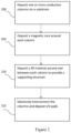
- Figure 2 shows the main steps in the fabrication process to obtain the inductor device of Fig. 1 .
- step 200 one or more columns of conductive material are deposited on a support substrate, the one or more columns comprising an input terminal and an output terminal.
- step 205 a magnetic layer in the form of a magnetic core is deposited around each column.
- step 210 a fill material is deposited around and between each column to provide a supporting structure.
- step 215 the columns are selectively interconnected with tracks of conductive material and I/O pads are deposited on the input terminal and the output terminal.
- the selective interconnection of the columns with tracks of conductive material is such that the first end of each intermediate column is conductively coupled to the first end of a first adjacent column and isolated from the first end of a second adjacent column and the second end of each intermediate column is conductively coupled to the second end of the second adjacent column and not coupled to the second end of the first adjacent column.
- the I/O pad for wire bonding/flip chip is then connected to the end of the input column and the end of the output column that is not connected to an intermediate column.
- Figure 3 shows a detailed schematic of one fabrication process to obtain the inductor device of Fig. 1b , where the device comprises an input column, an output column and at least one intermediate column.
- the first step of the fabrication process spaced apart columns of conductive material are deposited on a first support substrate (step 300).
- a first magnetic layer in the form of a magnetic core comprising alternating laminations of magnetic and dielectric materials is conformally deposited on and in between each column. This involves coating all of the exposed surfaces of the columns and the first support substrate with the magnetic core such that the magnetic core is deposited vertically around each column, horizontally on the first support substrate between each column, and horizontally on a first end of each column distal to the first support substrate.
- step 310 a fill material is deposited around and in the gaps between each column to provide a supporting structure.
- step 315 the surface of the supporting structure is planarized to remove the horizontal magnetic core deposited on the first end of each column.
- step 320 the intermediate columns are connected with a first set of conductive tracks such that the first end of each intermediate column is conductively coupled to the first end of a first adjacent column and isolated from the first end of a second adjacent column. I/O pads for wire bonding/flip chip may also be connected at this stage.
- step 325 a second support substrate is mounted to the first set of tracks of conductive material and the structure is inverted.
- step 330 the first support substrate is removed.
- step 335 the surface of a second end of each column is planarized in order to remove the horizontal magnetic core between each column.
- the intermediate columns are connected with a second set of interconnecting conductive tracks such that the second end of each intermediate column is conductively coupled to the second end of the second adjacent column and not coupled to the second end of the first adjacent column.
- a second I/O pad for wire bonding/flip chip may also be connected at this stage.
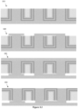
- Figure 4 shows a detailed schematic of another fabrication process to obtain the inductor device of Fig. 1b , where the device comprises an input column, an output column and at least one intermediate column.
- a plurality of lengths of a first insulating material are deposited on a support substrate, where a first set of tracks of conductive material are then deposited on those portions of the support substrate which are not in contact with the first insulating material. I/O pads may also be deposited at this stage (step 400).
- step 405 further first insulating material is deposited on the plurality of lengths of the first insulating material and also on selective portions of the first set of tracks of conductive material in order to form a plurality of spaced apart columns of the first insulating material.
- step 410 columns of conductive material are deposited between the plurality of spaced apart columns of insulating material such that a second end of each intermediate column is conductively coupled to the second end of a first adjacent column by the first set of tracks of conductive material and isolated from the second end of a second adjacent column.
- step 415 the first insulating material is removed.
- step 420 a thin film of a second insulating material is deposited on both the planar surfaces of the conductive columns and the support substrate.
- a first magnetic layer in the form of a magnetic core is then deposited around each column.
- step 425 a fill material is deposited around and in the gaps between each conductive column to form a supporting structure.
- step 430 the second insulating material on a first end of the conductive columns is removed.
- step 435 the intermediate columns are connected with a second set of interconnecting conductive tracks such that the first end of each intermediate column is conductively coupled to the first end of the second adjacent column and not coupled to the first end of the first adjacent column. I/O pads for wire bonding/flip chip may also be connected at this stage.
- FIG. 5 shows four additional alternative embodiments of the inductor device that do not form part of the present invention.
- each column is embedded in a magnetic layer formed by a magnetic core, which also acts as a supporting structure.
- the magnetic core comprises a solid sheet of magnetic material.
- Figures 5a and 5c shows a top down and a side view respectively of an alternative embodiment to Figure 5b , where the magnetic core comprises a plurality of rings concentric to each column, with a vertically-oriented intervening dielectric in between the rings.
- Figure 5e shows a side view of yet another embodiment, where the magnetic core comprises a plurality of rings concentric to each column of alternating horizontal laminations of magnetic and dielectric materials, with a vertically-oriented intervening dielectric in between the rings.
- Figure 5d shows an embodiment similar to Figure 5b , but where the magnetic core comprises a laminated solid sheet of alternating horizontal laminations of magnetic and dielectric materials.
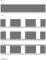
- Figure 6 shows a detailed schematic of an embodiment of the fabrication process to obtain the inductor device of the type shown in Figure 5b , where the device comprises an input column, an output column and at least one intermediate column.
- a plurality of spaced apart columns of a first insulating material are deposited on a first support substrate (600).
- step 605 columns of conductive material are then deposited between the plurality of spaced apart columns of the first insulating material.
- the first insulating material is removed.
- a second layer and a third layer of the same insulating material are deposited on the first support substrate. The second layer of insulating material makes contact with the support substrate and extends between the columns of conductive material.
- the third layer of insulating material is located on a portion of the surface of second layer of insulating material.
- a thin film of a fourth insulating material of a different type to the second and third layers of insulation is deposited on both the planar surfaces of the conductive columns and the second and third insulating layers.
- the second and third layers of insulating material are removed.
- a fifth insulation layer is deposited around the vertical sidewalls of the conductive columns.
- a magnetic layer is deposited in the spaces between the conductive columns so as to form a magnetic core and act as a supporting structure. The thickness of the magnetic core is equal to the thickness of the conductive columns.
- the magnetic core can be in the form of a solid sheet or take the form of rings which are concentric to each column, with a vertically-oriented dielectric in between the rings.
- the fourth insulating material is removed from the conductive columns.
- a sixth and a seventh layer of insulation is deposited on the surface of the magnetic core distal from the first support substrate.
- a seed layer is deposited on top of the sixth and seventh layers of insulation.
- the columns are connected with a first set of interconnecting conductive tracks such that a first end of each intermediate column is conductively coupled to the first end of a second adjacent column and not coupled to the first end of a first adjacent column.
- I/O pads for wire bonding/flip chip may also be connected at this stage.
- step 660 the surface of the first end of each column is planarized in order to remove the excess material.
- step 665 a second support substrate is mounted to the first set of tracks of conductive material and the structure is inverted.
- step 670 the first support substrate is removed.
- step 675 the columns are connected with a second set of interconnecting conductive tracks such that a second end of each intermediate column is conductively coupled to the second end of the first adjacent column and not coupled to the second end of the second adjacent column. I/O pads for wire bonding/flip chip may also be connected at this stage.
- Steps 600a to 630a show an alternative technique which can be performed in place of steps 600 to 630.
- a plurality of spaced apart conductive columns are deposited on a first support substrate (600a).
- a dielectric is deposited on all of the exposed surfaces of the columns and the first support substrate such that the dielectric is deposited vertically around each column, horizontally on the first support substrate between each column, and horizontally on a first end of each column distal to the first support substrate.
- a second support substrate is mounted to the columns and the structure is inverted.
- step 615a the first support substrate is removed.
- step 620a second and third layers of insulation material are deposited on the first support substrate.
- a dielectric is deposited on the horizontal surfaces of the columns and the second and third layers of insulation material.
- the second and third layers of insulation material are removed. The process then continues at step 635, as previously described.
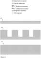
- Figure 7 shows a detailed schematic of one embodiment of the fabrication process to obtain the inductor device of the type shown in Figure 5d , where the device comprises an input column, an output column and at least one intermediate column.
- a magnetic layer in the form of a magnetic core which is in the form of a planar sheet comprising a plurality of alternating horizontal laminations of magnetic and dielectric materials, is deposited on a first support substrate (700).
- a selective etch creates discrete columnar voids in the magnetic core.
- a first insulation layer is deposited conformally, covering both the planar and vertical surfaces of the magnetic core.
- a second support substrate is mounted to the magnetic core and the structure is inverted.
- step 720 the first support substrate is removed.
- step 725 columns of conductive material are deposited into the discrete columnar voids in the magnetic core. The process then continues to step 645 of Figure 6 until step 670 of Figure 6 . Then, in step 730 the columns are connected with a second set of interconnecting conductive tracks such that a second end of each intermediate column is conductively coupled to the second end of the second adjacent column and not coupled to the second end of the first adjacent column. I/O pads for wire bonding/flip chip may also be connected at this stage.
- the magnetic core is in the form or a solid sheet.
- the magnetic core can take the form of rings which are concentric to each columnar void, with a vertically-oriented dielectric in between the rings.
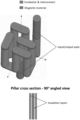
- Figure 8 shows a 3D view of the inductor device of Figure 1a along with a 90° cross-sectional view of a column of conductive material from that same structure (the supporting structure is not shown for clarity purposes).
- the column of conductive material is surrounded by a first magnetic layer in the form of a magnetic core, where the magnetic core may comprise laminations of alternating magnetic and dielectric materials.
- Figure 9a shows a 3D view of an embodiment of the inductor device of the present invention where the structure comprises a coaxial or concentric structure (the supporting structure is not shown for clarity purposes).
- This concentric structure provides a coupling of 0.9, as well as a perfect dc flux cancelation in the core. If the Re-Distribution Layer (RDL) top and bottom traces are placed on top of each other, a transformer with ultra-low leakage inductance and excellent coupling is achieved.
- RDL Re-Distribution Layer
- each concentric column comprises two individual columns of conductive material that are electrically insulated from one another, where each individual column of conductive material is further surrounded by a magnetic layer in the form of a magnetic core.
- the magnetic core comprises alternating vertical laminations of magnetic and dielectric materials.
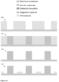
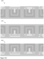
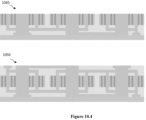
- Figure 10 shows a detailed schematic of the fabrication process of the inductor device shown in Figure 9 , where the device comprises an input column, an output column and at least one intermediate column.
- a first set of conductive columns is deposited on a first support substrate (1000).
- a first magnetic layer in the form of a magnetic core is conformally deposited on both the planar and vertical surfaces of the conductive columns and on the surface of the first support substrate between the columns.
- a layer of conductive material is conformally deposited on top of the first magnetic core, to form a second set of conductive columns concentric to the first set of conductive columns.
- a second magnetic layer in the form of a magnetic core is conformally deposited on top of the second set of conductive columns.
- a fill material is deposited around and in the gaps between the columns to provide a supporting structure.
- the surface of a first end of each column distal to the first support substrate is planarized in order to remove excess material on top of and between each column.
- a first set of interconnecting tracks of conductive material are deposited such that the first end of each intermediate column of the first set of columns is conductively coupled to the first end of a first adjacent column of the first set of columns and isolated from the first end of a second adjacent column of the first set of columns and the first end of each intermediate column of the second set of columns is conductively coupled to the first end of a first adjacent column of the second set of columns and isolated from the first end of a second adjacent column of the second set of columns, where the first set of interconnecting tracks of conductive material for the second set of conductive columns are electrically insulated from the first set of interconnecting tracks of conductive material for the first set of conductive columns.
- step 1035 a second support substrate is mounted to the first set of tracks of conductive material and the structure is inverted.
- step 1040 the first support substrate is removed.
- step 1045 the surface of a second end of each column is planarized in order to remove the horizontally-oriented material between each column.
- the columns are connected with a second set of interconnecting conductive tracks such that a second end of each intermediate column of the first set of columns is conductively coupled to the second end of the second adjacent column of the first set of columns and not coupled to the second end of the first adjacent column of the first set of columns and a second end of each intermediate column of the second set of columns is conductively coupled to the second end of the second adjacent column of the second set of columns and not coupled to the second end of the first adjacent column of the second set of columns, where the second set of interconnecting tracks of conductive material for the second set of conductive columns are electrically insulated from the second set of interconnecting tracks of conductive material for the first set of conductive columns. I/O pads for wire bonding/flip chip may also be connected at this stage.
- the conductive columns are located on square vertices.
- any other suitable arrangement of columns could equally well be used.
- the columns could be arranged in a honeycomb structure or connected in double helix form where the I/O pads are on adjacent columns to ease routing in the electrical circuit.
- a double helix form corresponds to two interleaved inductor devices that wind around each other like individual strands of deoxyribonucleic acid (DNA).
- the double-helical strands will ideally have a spiral topology, winding from a common centre outwards.
- the double-helical topology would have a reduced cross-sectional area, as opposed to a conventional toroidal structure, and the cross-section itself would consist of either an air core or a magnetic core, which would be in addition to the magnetic core which may or may not surround each of the individual columns.
- This double-helical form would result in the highest inductance with regards to topology.
- a space-filling arrangement of the columns such as for example, a curve, could also be used in order to ease routing.
- the inductor device discussed above provides a number of advantages over conventional planar structures. Firstly, and if considered as an inductor, the inductor device achieves high performance because of excellent coupling (that is, extremely low leakage inductance) and high efficiency.
- the structure has been found to offer 40% higher inductance for the same coil length when compared to existing V-groove inductors.
- the saturation current of this structure is 0.8A, which gives a current density of 4.3A/mm 2 .
- increasing the diameter of the conductive columns reduces the copper resistance and inductance of the columns, both, thus increasing the saturation current.
- a 12% inductance boost is also achieved.
- the inductor is implemented using copper columns embedded in magnetic material laminate, the inductance is increased by more than an order of magnitude (approximately 16 times).
- the present invention facilitates achieving efficient, high density in-package IVRs.
- the inductor structure When the inductor structure is integrated into an integrated voltage regulator circuit, the interconnections between different components on the circuit are being used to act as passive devices in the form of inductors. This results in a fully integrated VR solution where the active circuitry is either monolithically built or packaged with the passive devices, that is the inductors and capacitors. Further, the inductor structure uses its magnetic core to improve the power density and efficiency of the IVR circuit.
- Figure 11 shows another embodiment of the inductor device that does not form part of the present invention.
- the supporting structure comprises a passivation layer, as was the case for Figure 1a and 1b .
- the width of the passivation layer was much smaller than the width of the magnetic layer, whereas in the embodiment of Figure 11 , the passivation layer is far greater than the width of the magnetic layer.
- Figure 12 shows another embodiment of the inductor device that does not form part of the present invention, where the supporting structure comprises a combination of the interconnecting tracks of conductive material and a passivation layer. It should be noted that the interconnect can support the device due to the short distance (small volume) between the conductive columns.
- Figure 13 shows another embodiment of the inductor device that does not form part of the present invention, where the supporting structure comprises the interconnecting tracks of conductive material and the conductive columns.
- the supporting structure comprises the interconnecting tracks of conductive material and the conductive columns.
- air is used as a dielectric.
- this device is not an air core inductor.
- This embodiment is discrete and self-supporting, as the small length of the interconnecting tracks results in tiny voids between the columns of conductive material, which overall closely approximates a solid structure with a continuous cross-section.
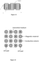
- Figure 14 shows a top down view of the inductor array of Figure 8. It can be seen that in this embodiment, the columns of conductive material embedded in the supporting structure (not shown) are separated by an interstitial medium.
- the supporting structure comprises the material which provides the mechanical strength of the device.
- a mechanically strong device is synonymously described as being either discrete or self-supporting, or both. A discrete and/or self-supporting device is thus able to "stand on its own” without being supported by any external forces or bodies, such as for example a semiconducting substrate or a printed circuit board.
- the interstitial medium comprises the material that fills the vertically-oriented space between the columns of conductive material.
- the supporting structure and the interstitial medium may or may not be the same material, depending on the embodiment.
- Figures 5 and Figures 11 to 13 also comprise columns of conductive material embedded in a supporting structure and separated by an interstitial medium.
- the interstitial medium may be a gas, a magnetic material or a non-conductive and non-magnetic material.
- the interstitial medium comprises a gas in the embodiment of Figure 13
- the supporting structure comprises the interconnecting tracks of conductive material and the columns of conductive material.
- the supporting structure and the interstitial medium both comprise the same material, which is a non-conductive and non-magnetic material.
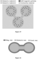
- Figure 15 comprises a variation of the embodiment of Figure 5a .
- the rings of magnetic material comprise magnetic particles suspended in a polymer matrix.
- the supporting structure is not a semiconductor, glass or a PCB material.
- the coupling factor between two inductors can be tuned by varying the width of the adjoining dielectric.
- the width of the dielectric material shown in Figure 16 can be adjusted to tune the coupling between the inductors to a desired value.
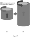
- the magnetic anisotropy direction is partially a function of the aspect ratio (AR) of the conductive columns, i.e. the ratio of the height of a conductive column to the diameter of a conductive column.
- AR aspect ratio
Landscapes
- Engineering & Computer Science (AREA)
- Power Engineering (AREA)
- Microelectronics & Electronic Packaging (AREA)
- Manufacturing & Machinery (AREA)
- Coils Or Transformers For Communication (AREA)
Claims (6)
- Transformator oder gekoppelte Induktionsvorrichtung, umfassend:zwei miteinander verbundene vertikale Säulen aus leitfähigem Material, die sich von einem Substrat erstrecken und in eine Trägerstruktur eingebettet sind, wobei die zwei miteinander verbundenen vertikalen Säulen eine erste Säule und eine von der ersten Säule beabstandete zweite Säule umfassen, wobei jede Säule einen inneren Säulenteil und einen mit dem inneren Säulenteil konzentrischen äußeren Säulenteil umfasst,wobei der äußere Säulenteil und der innere Säulenteil jeweils ein erstes Ende und ein zweites Ende aufweisen, wobei das erste Ende des ersten inneren Säulenteils und des ersten äußeren Säulenteils jeweils einen Eingangsanschluss oder einen Ausgangsanschluss umfassen und das erste Ende des zweiten inneren Säulenteils und des zweiten äußeren Säulenteils jeweils einen Eingangsanschluss oder einen Ausgangsanschluss umfassen und wobei das zweite Ende des ersten inneren Säulenteils durch eine innere Verbindungsbahn aus leitfähigem Material leitfähig mit dem zweiten Ende des zweiten inneren Säulenteils gekoppelt ist und wobei das zweite Ende des ersten äußeren Säulenteils durch eine äußere Verbindungsbahn aus leitfähigem Material leitfähig mit dem zweiten Ende des zweiten äußeren Säulenteils gekoppelt ist; dadurch gekennzeichnet, dassdie Vorrichtung ferner eine erste magnetische Schicht, die jeden äußeren Säulenteil umgibt, und eine zweite magnetische Schicht, die jeden inneren Säulenteil umgibt, umfasst, wobei die erste und die zweite magnetische Schicht eine Mehrzahl von vertikalen Laminierungen umfassen, die abwechselnde magnetische und dielektrische Schichten umfassen, wobei die zweite magnetische Schicht zwischen jedem inneren Säulenteil und äußeren Säulenteil bereitgestellt ist.
- Transformator oder gekoppelte Induktionsvorrichtung, umfassend:drei oder mehr miteinander verbundene, voneinander beabstandete vertikale Säulen aus leitfähigem Material, die sich von einem Substrat erstrecken und in eine Trägerstruktur eingebettet sind, wobei die drei oder mehr vertikalen Säulen eine Eingangssäule, eine Ausgangssäule und mindestens eine Zwischensäule umfassen, wobei jede vertikale Säule einen inneren Säulenteil und einen mit dem inneren Säulenteil konzentrischen äußeren Säulenteil umfasst, wobei der äußere Säulenteil und der innere Säulenteil jeweils ein erstes Ende und ein zweites Ende aufweisen,wobei das erste Ende jedes inneren Zwischensäulenteils durch eine erste innere Verbindungsbahn aus leitfähigem Material leitfähig mit dem ersten Ende eines ersten benachbarten inneren Säulenteils gekoppelt ist und von dem ersten Ende eines zweiten benachbarten inneren Säulenteils isoliert ist und das zweite Ende jedes inneren Zwischensäulenteils durch eine zweite innere Verbindungsbahn aus leitfähigem Material leitfähig mit dem zweiten Ende des zweiten benachbarten inneren Säulenteils gekoppelt ist und von dem zweiten Ende des ersten benachbarten inneren Säulenteils isoliert ist;und wobei das erste Ende jedes äußeren Zwischensäulenteils durch eine erste äußere Verbindungsbahn aus leitfähigem Material leitfähig mit dem ersten Ende eines ersten benachbarten äußeren Säulenteils gekoppelt ist und von dem ersten Ende eines zweiten benachbarten äußeren Säulenteils isoliert ist und das zweite Ende jedes äußeren Zwischensäulenteils durch eine zweite äußere Verbindungsbahn aus leitfähigem Material leitfähig mit dem zweiten Ende des zweiten benachbarten äußeren Säulenteils gekoppelt ist und von dem zweiten Ende des ersten benachbarten äußeren Säulenteils isoliert ist;wobei jedes Ende eines inneren Säulenteils und eines äußeren Säulenteils, das nicht mit einer Zwischensäule verbunden ist, einen Eingangsanschluss oder einen Ausgangsanschluss umfasst,dadurch gekennzeichnet, dass die Vorrichtung ferner eine erste magnetische Schicht, die jeden äußeren Säulenteil umgibt, und eine zweite magnetische Schicht, die jeden inneren Säulenteil umgibt, umfasst, wobei die erste und die zweite magnetische Schicht eine Mehrzahl von vertikalen Laminierungen umfassen, die abwechselnde magnetische und dielektrische Schichten umfassen; und wobei die zweite magnetische Schicht zwischen jedem inneren Säulenteil und äußeren Säulenteil bereitgestellt ist.
- Vorrichtung nach einem der vorhergehenden Ansprüche, wobei die Trägerstruktur ein nichtleitfähiges und nichtmagnetisches Material umfasst.
- Vorrichtung nach einem der vorhergehenden Ansprüche, wobei die erste magnetische Schicht eine Mehrzahl von Ringen aus magnetischem Material umfasst, wobei jede Säule von einem Ring umgeben ist, und die ferner eine Isolierschicht zwischen jedem der Ringe umfasst.
- Vorrichtung nach einem der vorhergehenden Ansprüche, wobei die erste und/oder zweite magnetische Schicht magnetische Teilchen umfasst, die in einer Polymermatrix suspendiert sind.
- Vorrichtung nach einem der vorhergehenden Ansprüche, wobei die erste magnetische Schicht und/oder die zweite magnetische Schicht eine solche magnetische Anisotropie aufweist, dass die schwere Achse in Umfangsrichtung zu den Säulen ausgerichtet ist.
Applications Claiming Priority (3)
| Application Number | Priority Date | Filing Date | Title |
|---|---|---|---|
| US201862745901P | 2018-10-15 | 2018-10-15 | |
| GBGB1816833.6A GB201816833D0 (en) | 2018-10-16 | 2018-10-16 | A vertical magnetic structure for integrated power conversion |
| PCT/EP2019/077978 WO2020079002A1 (en) | 2018-10-15 | 2019-10-15 | A vertical magnetic structure for integrated power conversion |
Publications (3)
| Publication Number | Publication Date |
|---|---|
| EP3867933A1 EP3867933A1 (de) | 2021-08-25 |
| EP3867933B1 true EP3867933B1 (de) | 2025-06-18 |
| EP3867933C0 EP3867933C0 (de) | 2025-06-18 |
Family
ID=64397629
Family Applications (1)
| Application Number | Title | Priority Date | Filing Date |
|---|---|---|---|
| EP19801203.1A Active EP3867933B1 (de) | 2018-10-15 | 2019-10-15 | Eine vertikale magnetische struktur zur integrierten leistungskonversion |
Country Status (4)
| Country | Link |
|---|---|
| US (2) | US12217891B2 (de) |
| EP (1) | EP3867933B1 (de) |
| GB (1) | GB201816833D0 (de) |
| WO (1) | WO2020079002A1 (de) |
Families Citing this family (4)
| Publication number | Priority date | Publication date | Assignee | Title |
|---|---|---|---|---|
| GB202119005D0 (en) * | 2021-12-24 | 2022-02-09 | Univ College Cork National Univ Of Ireland Cork | Magnetic component integration |
| CN114937603A (zh) * | 2022-03-25 | 2022-08-23 | 珠海越亚半导体股份有限公司 | 具有滤波功能的导通基板、载板布线结构及其制作方法 |
| US20240332100A1 (en) * | 2023-03-30 | 2024-10-03 | Intel Corporation | Glass-integrated inductors in integrated circuit packages |
| US20240371799A1 (en) * | 2023-05-05 | 2024-11-07 | Intel Corporation | Through core via coaxial-type inductors with two or more magnetic materials for power delivery applications |
Family Cites Families (13)
| Publication number | Priority date | Publication date | Assignee | Title |
|---|---|---|---|---|
| JP3600415B2 (ja) * | 1997-07-15 | 2004-12-15 | 株式会社東芝 | 分布定数素子 |
| JP2002289419A (ja) * | 2001-01-19 | 2002-10-04 | Tdk Corp | 軟磁性合金厚膜及び磁気素子並びにそれらの製造方法 |
| US8440917B2 (en) * | 2007-11-19 | 2013-05-14 | International Business Machines Corporation | Method and apparatus to reduce impedance discontinuity in packages |
| US9921640B2 (en) * | 2012-09-28 | 2018-03-20 | Intel Corporation | Integrated voltage regulators with magnetically enhanced inductors |
| US20140104284A1 (en) * | 2012-10-16 | 2014-04-17 | Qualcomm Mems Technologies, Inc. | Through substrate via inductors |
| JP5871329B2 (ja) * | 2013-03-15 | 2016-03-01 | サムソン エレクトロ−メカニックス カンパニーリミテッド. | インダクタ及びその製造方法 |
| US9384883B2 (en) * | 2014-01-14 | 2016-07-05 | Qualcomm Incorporated | Nested through glass via transformer |
| JP2015135870A (ja) | 2014-01-16 | 2015-07-27 | 富士通株式会社 | インダクタ装置及びインダクタ装置の製造方法 |
| KR101900879B1 (ko) | 2015-10-16 | 2018-09-21 | 주식회사 모다이노칩 | 파워 인덕터 |
| US9959964B2 (en) * | 2015-11-13 | 2018-05-01 | Qualcomm Incorporated | Thin film magnet inductor structure for high quality (Q)-factor radio frequency (RF) applications |
| EP3493227B1 (de) | 2016-09-02 | 2023-01-25 | Murata Manufacturing Co., Ltd. | Induktorkomponente und stromversorgungsmodul |
| KR102145921B1 (ko) * | 2017-01-03 | 2020-08-28 | 엘지이노텍 주식회사 | 인덕터 및 이를 포함하는 emi 필터 |
| CN106653318B (zh) | 2017-02-28 | 2019-06-18 | 华为技术有限公司 | 电感器件和交错并联直流变换器 |
-
2018
- 2018-10-16 GB GBGB1816833.6A patent/GB201816833D0/en not_active Ceased
-
2019
- 2019-10-15 EP EP19801203.1A patent/EP3867933B1/de active Active
- 2019-10-15 US US17/285,751 patent/US12217891B2/en active Active
- 2019-10-15 WO PCT/EP2019/077978 patent/WO2020079002A1/en not_active Ceased
-
2024
- 2024-12-26 US US19/002,326 patent/US20250357033A1/en active Pending
Also Published As
| Publication number | Publication date |
|---|---|
| WO2020079002A1 (en) | 2020-04-23 |
| GB201816833D0 (en) | 2018-11-28 |
| EP3867933A1 (de) | 2021-08-25 |
| US20250357033A1 (en) | 2025-11-20 |
| EP3867933C0 (de) | 2025-06-18 |
| US12217891B2 (en) | 2025-02-04 |
| US20220005640A1 (en) | 2022-01-06 |
Similar Documents
| Publication | Publication Date | Title |
|---|---|---|
| US20250357033A1 (en) | Vertical magnetic structure for integrated power conversion | |
| US8907447B2 (en) | Power inductors in silicon | |
| US8212155B1 (en) | Integrated passive device | |
| US7948346B2 (en) | Planar grooved power inductor structure and method | |
| US7107666B2 (en) | Method of manufacturing an ultra-miniature magnetic device | |
| US9027229B2 (en) | Coil assembly comprising planar coil | |
| US8786393B1 (en) | Step up or step down micro-transformer with tight magnetic coupling | |
| TWI680552B (zh) | 具有貫穿基板通路核心的三維互連多晶粒電感器 | |
| US20080252407A1 (en) | Multi-Layer Inductive Element for Integrated Circuit | |
| US6738240B1 (en) | Microtransformer for system-on-chip power supply | |
| US10163558B2 (en) | Vertically stacked inductors and transformers | |
| US20050105225A1 (en) | Microtransformer for system-on-chip power supply | |
| CN110546779A (zh) | 具有经耦合贯穿衬底通路核心的多裸片电感器 | |
| JP4505201B2 (ja) | 3−dスパイラル積層インダクタおよび3−dスパイラル積層インダクタを形成する方法 | |
| KR20190032226A (ko) | 집적 인덕터를 내부에 갖는 반도체 구조체 | |
| US6420954B1 (en) | Coupled multilayer soft magnetic films for high frequency microtransformer for system-on-chip power supply | |
| JP2000082621A (ja) | 平面トランス | |
| US20250166881A1 (en) | Layered process-constructed double-winding embedded solenoid inductor | |
| EP4462455A2 (de) | Auf leiterplatte basierende wicklungsstruktur für induktoren | |
| WO2026001662A1 (zh) | 集成于封装基板的电感、半导体器件及制备方法 |
Legal Events
| Date | Code | Title | Description |
|---|---|---|---|
| STAA | Information on the status of an ep patent application or granted ep patent |
Free format text: STATUS: UNKNOWN |
|
| STAA | Information on the status of an ep patent application or granted ep patent |
Free format text: STATUS: THE INTERNATIONAL PUBLICATION HAS BEEN MADE |
|
| PUAI | Public reference made under article 153(3) epc to a published international application that has entered the european phase |
Free format text: ORIGINAL CODE: 0009012 |
|
| STAA | Information on the status of an ep patent application or granted ep patent |
Free format text: STATUS: REQUEST FOR EXAMINATION WAS MADE |
|
| 17P | Request for examination filed |
Effective date: 20210507 |
|
| AK | Designated contracting states |
Kind code of ref document: A1 Designated state(s): AL AT BE BG CH CY CZ DE DK EE ES FI FR GB GR HR HU IE IS IT LI LT LU LV MC MK MT NL NO PL PT RO RS SE SI SK SM TR |
|
| DAV | Request for validation of the european patent (deleted) | ||
| DAX | Request for extension of the european patent (deleted) | ||
| STAA | Information on the status of an ep patent application or granted ep patent |
Free format text: STATUS: EXAMINATION IS IN PROGRESS |
|
| 17Q | First examination report despatched |
Effective date: 20230328 |
|
| RIC1 | Information provided on ipc code assigned before grant |
Ipc: H05K 1/16 20060101ALI20241127BHEP Ipc: H05K 1/11 20060101ALI20241127BHEP Ipc: H01F 41/04 20060101ALI20241127BHEP Ipc: H01F 27/28 20060101ALI20241127BHEP Ipc: H01F 17/00 20060101AFI20241127BHEP |
|
| GRAP | Despatch of communication of intention to grant a patent |
Free format text: ORIGINAL CODE: EPIDOSNIGR1 |
|
| STAA | Information on the status of an ep patent application or granted ep patent |
Free format text: STATUS: GRANT OF PATENT IS INTENDED |
|
| INTG | Intention to grant announced |
Effective date: 20250109 |
|
| GRAS | Grant fee paid |
Free format text: ORIGINAL CODE: EPIDOSNIGR3 |
|
| GRAA | (expected) grant |
Free format text: ORIGINAL CODE: 0009210 |
|
| STAA | Information on the status of an ep patent application or granted ep patent |
Free format text: STATUS: THE PATENT HAS BEEN GRANTED |
|
| AK | Designated contracting states |
Kind code of ref document: B1 Designated state(s): AL AT BE BG CH CY CZ DE DK EE ES FI FR GB GR HR HU IE IS IT LI LT LU LV MC MK MT NL NO PL PT RO RS SE SI SK SM TR |
|
| REG | Reference to a national code |
Ref country code: GB Ref legal event code: FG4D |
|
| REG | Reference to a national code |
Ref country code: CH Ref legal event code: EP |
|
| REG | Reference to a national code |
Ref country code: DE Ref legal event code: R096 Ref document number: 602019071319 Country of ref document: DE |
|
| REG | Reference to a national code |
Ref country code: CH Ref legal event code: EP |
|
| REG | Reference to a national code |
Ref country code: IE Ref legal event code: FG4D |
|
| U01 | Request for unitary effect filed |
Effective date: 20250718 |
|
| U07 | Unitary effect registered |
Designated state(s): AT BE BG DE DK EE FI FR IT LT LU LV MT NL PT RO SE SI Effective date: 20250730 |
|
| PG25 | Lapsed in a contracting state [announced via postgrant information from national office to epo] |
Ref country code: GR Free format text: LAPSE BECAUSE OF FAILURE TO SUBMIT A TRANSLATION OF THE DESCRIPTION OR TO PAY THE FEE WITHIN THE PRESCRIBED TIME-LIMIT Effective date: 20250919 Ref country code: NO Free format text: LAPSE BECAUSE OF FAILURE TO SUBMIT A TRANSLATION OF THE DESCRIPTION OR TO PAY THE FEE WITHIN THE PRESCRIBED TIME-LIMIT Effective date: 20250918 |
|
| PG25 | Lapsed in a contracting state [announced via postgrant information from national office to epo] |
Ref country code: HR Free format text: LAPSE BECAUSE OF FAILURE TO SUBMIT A TRANSLATION OF THE DESCRIPTION OR TO PAY THE FEE WITHIN THE PRESCRIBED TIME-LIMIT Effective date: 20250618 |
|
| PG25 | Lapsed in a contracting state [announced via postgrant information from national office to epo] |
Ref country code: RS Free format text: LAPSE BECAUSE OF FAILURE TO SUBMIT A TRANSLATION OF THE DESCRIPTION OR TO PAY THE FEE WITHIN THE PRESCRIBED TIME-LIMIT Effective date: 20250918 |
|
| U20 | Renewal fee for the european patent with unitary effect paid |
Year of fee payment: 7 Effective date: 20251030 |
|
| PG25 | Lapsed in a contracting state [announced via postgrant information from national office to epo] |
Ref country code: IS Free format text: LAPSE BECAUSE OF FAILURE TO SUBMIT A TRANSLATION OF THE DESCRIPTION OR TO PAY THE FEE WITHIN THE PRESCRIBED TIME-LIMIT Effective date: 20251018 |
|
| PG25 | Lapsed in a contracting state [announced via postgrant information from national office to epo] |
Ref country code: SM Free format text: LAPSE BECAUSE OF FAILURE TO SUBMIT A TRANSLATION OF THE DESCRIPTION OR TO PAY THE FEE WITHIN THE PRESCRIBED TIME-LIMIT Effective date: 20250618 |
|
| PG25 | Lapsed in a contracting state [announced via postgrant information from national office to epo] |
Ref country code: CZ Free format text: LAPSE BECAUSE OF FAILURE TO SUBMIT A TRANSLATION OF THE DESCRIPTION OR TO PAY THE FEE WITHIN THE PRESCRIBED TIME-LIMIT Effective date: 20250618 |
|
| PG25 | Lapsed in a contracting state [announced via postgrant information from national office to epo] |
Ref country code: PL Free format text: LAPSE BECAUSE OF FAILURE TO SUBMIT A TRANSLATION OF THE DESCRIPTION OR TO PAY THE FEE WITHIN THE PRESCRIBED TIME-LIMIT Effective date: 20250618 |
|
| PG25 | Lapsed in a contracting state [announced via postgrant information from national office to epo] |
Ref country code: SK Free format text: LAPSE BECAUSE OF FAILURE TO SUBMIT A TRANSLATION OF THE DESCRIPTION OR TO PAY THE FEE WITHIN THE PRESCRIBED TIME-LIMIT Effective date: 20250618 |
|
| PG25 | Lapsed in a contracting state [announced via postgrant information from national office to epo] |
Ref country code: ES Free format text: LAPSE BECAUSE OF FAILURE TO SUBMIT A TRANSLATION OF THE DESCRIPTION OR TO PAY THE FEE WITHIN THE PRESCRIBED TIME-LIMIT Effective date: 20250618 |
|
| PLBE | No opposition filed within time limit |
Free format text: ORIGINAL CODE: 0009261 |
|
| STAA | Information on the status of an ep patent application or granted ep patent |
Free format text: STATUS: NO OPPOSITION FILED WITHIN TIME LIMIT |
|
| REG | Reference to a national code |
Ref country code: CH Ref legal event code: L10 Free format text: ST27 STATUS EVENT CODE: U-0-0-L10-L00 (AS PROVIDED BY THE NATIONAL OFFICE) Effective date: 20260430 |