EP3863830B1 - Verfahren zur herstellung eines mehrschichtkörpers und ein mehrschichtkörper - Google Patents
Verfahren zur herstellung eines mehrschichtkörpers und ein mehrschichtkörper Download PDFInfo
- Publication number
- EP3863830B1 EP3863830B1 EP19782547.4A EP19782547A EP3863830B1 EP 3863830 B1 EP3863830 B1 EP 3863830B1 EP 19782547 A EP19782547 A EP 19782547A EP 3863830 B1 EP3863830 B1 EP 3863830B1
- Authority
- EP
- European Patent Office
- Prior art keywords
- sensor
- substrate
- film
- films
- relief
- Prior art date
- Legal status (The legal status is an assumption and is not a legal conclusion. Google has not performed a legal analysis and makes no representation as to the accuracy of the status listed.)
- Active
Links
Images


Classifications
-
- B—PERFORMING OPERATIONS; TRANSPORTING
- B29—WORKING OF PLASTICS; WORKING OF SUBSTANCES IN A PLASTIC STATE IN GENERAL
- B29C—SHAPING OR JOINING OF PLASTICS; SHAPING OF MATERIAL IN A PLASTIC STATE, NOT OTHERWISE PROVIDED FOR; AFTER-TREATMENT OF THE SHAPED PRODUCTS, e.g. REPAIRING
- B29C45/00—Injection moulding, i.e. forcing the required volume of moulding material through a nozzle into a closed mould; Apparatus therefor
- B29C45/14—Injection moulding, i.e. forcing the required volume of moulding material through a nozzle into a closed mould; Apparatus therefor incorporating preformed parts or layers, e.g. injection moulding around inserts or for coating articles
-
- B—PERFORMING OPERATIONS; TRANSPORTING
- B29—WORKING OF PLASTICS; WORKING OF SUBSTANCES IN A PLASTIC STATE IN GENERAL
- B29C—SHAPING OR JOINING OF PLASTICS; SHAPING OF MATERIAL IN A PLASTIC STATE, NOT OTHERWISE PROVIDED FOR; AFTER-TREATMENT OF THE SHAPED PRODUCTS, e.g. REPAIRING
- B29C51/00—Shaping by thermoforming, i.e. shaping sheets or sheet like preforms after heating, e.g. shaping sheets in matched moulds or by deep-drawing; Apparatus therefor
- B29C51/12—Shaping by thermoforming, i.e. shaping sheets or sheet like preforms after heating, e.g. shaping sheets in matched moulds or by deep-drawing; Apparatus therefor of articles having inserts or reinforcements
-
- B—PERFORMING OPERATIONS; TRANSPORTING
- B29—WORKING OF PLASTICS; WORKING OF SUBSTANCES IN A PLASTIC STATE IN GENERAL
- B29C—SHAPING OR JOINING OF PLASTICS; SHAPING OF MATERIAL IN A PLASTIC STATE, NOT OTHERWISE PROVIDED FOR; AFTER-TREATMENT OF THE SHAPED PRODUCTS, e.g. REPAIRING
- B29C51/00—Shaping by thermoforming, i.e. shaping sheets or sheet like preforms after heating, e.g. shaping sheets in matched moulds or by deep-drawing; Apparatus therefor
- B29C51/14—Shaping by thermoforming, i.e. shaping sheets or sheet like preforms after heating, e.g. shaping sheets in matched moulds or by deep-drawing; Apparatus therefor using multilayered preforms or sheets
-
- B—PERFORMING OPERATIONS; TRANSPORTING
- B29—WORKING OF PLASTICS; WORKING OF SUBSTANCES IN A PLASTIC STATE IN GENERAL
- B29C—SHAPING OR JOINING OF PLASTICS; SHAPING OF MATERIAL IN A PLASTIC STATE, NOT OTHERWISE PROVIDED FOR; AFTER-TREATMENT OF THE SHAPED PRODUCTS, e.g. REPAIRING
- B29C51/00—Shaping by thermoforming, i.e. shaping sheets or sheet like preforms after heating, e.g. shaping sheets in matched moulds or by deep-drawing; Apparatus therefor
- B29C51/16—Lining or labelling
-
- B—PERFORMING OPERATIONS; TRANSPORTING
- B29—WORKING OF PLASTICS; WORKING OF SUBSTANCES IN A PLASTIC STATE IN GENERAL
- B29C—SHAPING OR JOINING OF PLASTICS; SHAPING OF MATERIAL IN A PLASTIC STATE, NOT OTHERWISE PROVIDED FOR; AFTER-TREATMENT OF THE SHAPED PRODUCTS, e.g. REPAIRING
- B29C63/00—Lining or sheathing, i.e. applying preformed layers or sheathings of plastics; Apparatus therefor
- B29C63/02—Lining or sheathing, i.e. applying preformed layers or sheathings of plastics; Apparatus therefor using sheet or web-like material
-
- B—PERFORMING OPERATIONS; TRANSPORTING
- B29—WORKING OF PLASTICS; WORKING OF SUBSTANCES IN A PLASTIC STATE IN GENERAL
- B29C—SHAPING OR JOINING OF PLASTICS; SHAPING OF MATERIAL IN A PLASTIC STATE, NOT OTHERWISE PROVIDED FOR; AFTER-TREATMENT OF THE SHAPED PRODUCTS, e.g. REPAIRING
- B29C63/00—Lining or sheathing, i.e. applying preformed layers or sheathings of plastics; Apparatus therefor
- B29C63/22—Lining or sheathing, i.e. applying preformed layers or sheathings of plastics; Apparatus therefor using layers or sheathings having a shape adapted to the shape of the article
-
- B—PERFORMING OPERATIONS; TRANSPORTING
- B29—WORKING OF PLASTICS; WORKING OF SUBSTANCES IN A PLASTIC STATE IN GENERAL
- B29C—SHAPING OR JOINING OF PLASTICS; SHAPING OF MATERIAL IN A PLASTIC STATE, NOT OTHERWISE PROVIDED FOR; AFTER-TREATMENT OF THE SHAPED PRODUCTS, e.g. REPAIRING
- B29C2791/00—Shaping characteristics in general
- B29C2791/004—Shaping under special conditions
- B29C2791/009—Using laser
-
- B—PERFORMING OPERATIONS; TRANSPORTING
- B29—WORKING OF PLASTICS; WORKING OF SUBSTANCES IN A PLASTIC STATE IN GENERAL
- B29C—SHAPING OR JOINING OF PLASTICS; SHAPING OF MATERIAL IN A PLASTIC STATE, NOT OTHERWISE PROVIDED FOR; AFTER-TREATMENT OF THE SHAPED PRODUCTS, e.g. REPAIRING
- B29C2793/00—Shaping techniques involving a cutting or machining operation
- B29C2793/0027—Cutting off
-
- B—PERFORMING OPERATIONS; TRANSPORTING
- B29—WORKING OF PLASTICS; WORKING OF SUBSTANCES IN A PLASTIC STATE IN GENERAL
- B29C—SHAPING OR JOINING OF PLASTICS; SHAPING OF MATERIAL IN A PLASTIC STATE, NOT OTHERWISE PROVIDED FOR; AFTER-TREATMENT OF THE SHAPED PRODUCTS, e.g. REPAIRING
- B29C2793/00—Shaping techniques involving a cutting or machining operation
- B29C2793/0045—Perforating
-
- B—PERFORMING OPERATIONS; TRANSPORTING
- B29—WORKING OF PLASTICS; WORKING OF SUBSTANCES IN A PLASTIC STATE IN GENERAL
- B29L—INDEXING SCHEME ASSOCIATED WITH SUBCLASS B29C, RELATING TO PARTICULAR ARTICLES
- B29L2031/00—Other particular articles
- B29L2031/34—Electrical apparatus, e.g. sparking plugs or parts thereof
- B29L2031/3406—Components, e.g. resistors
-
- B—PERFORMING OPERATIONS; TRANSPORTING
- B29—WORKING OF PLASTICS; WORKING OF SUBSTANCES IN A PLASTIC STATE IN GENERAL
- B29L—INDEXING SCHEME ASSOCIATED WITH SUBCLASS B29C, RELATING TO PARTICULAR ARTICLES
- B29L2031/00—Other particular articles
- B29L2031/34—Electrical apparatus, e.g. sparking plugs or parts thereof
- B29L2031/3425—Printed circuits
-
- B—PERFORMING OPERATIONS; TRANSPORTING
- B29—WORKING OF PLASTICS; WORKING OF SUBSTANCES IN A PLASTIC STATE IN GENERAL
- B29L—INDEXING SCHEME ASSOCIATED WITH SUBCLASS B29C, RELATING TO PARTICULAR ARTICLES
- B29L2031/00—Other particular articles
- B29L2031/34—Electrical apparatus, e.g. sparking plugs or parts thereof
- B29L2031/3443—Switches
-
- B—PERFORMING OPERATIONS; TRANSPORTING
- B29—WORKING OF PLASTICS; WORKING OF SUBSTANCES IN A PLASTIC STATE IN GENERAL
- B29L—INDEXING SCHEME ASSOCIATED WITH SUBCLASS B29C, RELATING TO PARTICULAR ARTICLES
- B29L2031/00—Other particular articles
- B29L2031/34—Electrical apparatus, e.g. sparking plugs or parts thereof
- B29L2031/3481—Housings or casings incorporating or embedding electric or electronic elements
-
- B—PERFORMING OPERATIONS; TRANSPORTING
- B29—WORKING OF PLASTICS; WORKING OF SUBSTANCES IN A PLASTIC STATE IN GENERAL
- B29L—INDEXING SCHEME ASSOCIATED WITH SUBCLASS B29C, RELATING TO PARTICULAR ARTICLES
- B29L2031/00—Other particular articles
- B29L2031/744—Labels, badges, e.g. marker sleeves
-
- B—PERFORMING OPERATIONS; TRANSPORTING
- B31—MAKING ARTICLES OF PAPER, CARDBOARD OR MATERIAL WORKED IN A MANNER ANALOGOUS TO PAPER; WORKING PAPER, CARDBOARD OR MATERIAL WORKED IN A MANNER ANALOGOUS TO PAPER
- B31D—MAKING ARTICLES OF PAPER, CARDBOARD OR MATERIAL WORKED IN A MANNER ANALOGOUS TO PAPER, NOT PROVIDED FOR IN SUBCLASSES B31B OR B31C
- B31D1/00—Multiple-step processes for making flat articles ; Making flat articles
- B31D1/02—Multiple-step processes for making flat articles ; Making flat articles the articles being labels or tags
- B31D1/021—Making adhesive labels having a multilayered structure, e.g. provided on carrier webs
-
- G—PHYSICS
- G06—COMPUTING OR CALCULATING; COUNTING
- G06F—ELECTRIC DIGITAL DATA PROCESSING
- G06F2203/00—Indexing scheme relating to G06F3/00 - G06F3/048
- G06F2203/041—Indexing scheme relating to G06F3/041 - G06F3/045
- G06F2203/04103—Manufacturing, i.e. details related to manufacturing processes specially suited for touch sensitive devices
-
- G—PHYSICS
- G09—EDUCATION; CRYPTOGRAPHY; DISPLAY; ADVERTISING; SEALS
- G09F—DISPLAYING; ADVERTISING; SIGNS; LABELS OR NAME-PLATES; SEALS
- G09F3/00—Labels, tag tickets, or similar identification or indication means; Seals; Postage or like stamps
- G09F3/04—Labels, tag tickets, or similar identification or indication means; Seals; Postage or like stamps to be fastened or secured by the material of the label itself, e.g. by thermo-adhesion
Definitions
- the invention relates to a method for producing a multilayer body and to a multilayer body.
- Such a sensor film is, for example, DE 10 2011 111 506 A1
- This sensor film has a carrier film onto which transparent conductor tracks are applied. By appropriately arranging or overlaying these conductor tracks, capacitive touch sensors are formed in the sensor film.
- the documents US 2016/0192474 A1 , US 2003/0121767 A1 , DE 203 08 525 U1 , DE 203 07 486 U1 , US2006104037A1 and US 6 824 321 B1 each describe a multilayer body and a method for producing the multilayer body using a thermoforming process.
- the document JP 6 140 769 B2 describes a multilayer body whose surface relief is caused by a deformation mechanism based on tension/compression mechanisms, piezoelectric materials, or microelectronic-mechanical system elements.
- the object is achieved by a method for producing a multi-layer body according to claim 1.
- Such a method for producing a multilayer body and such a multilayer body are characterized by the fact that, through the selection of the process parameters and the materials used for the components of the multilayer body, such as the components of the sensor films and/or the substrate, a surface relief is created on the first surface of the substrate facing away from the sensor film.
- the sensor film and the sensor area of the sensor film are thus protected from environmental influences by the substrate. Since the substrate is manufactured separately before being combined with the sensor film, dimensionally stable and chemically resistant materials can be used for the substrate, which are not compatible with the processes used in the production of the sensor film for producing the delicate conductor tracks for providing the sensor functionality.
- the method according to the invention ensures that a surface relief is formed on the surface of the substrate facing away from the sensor film, which, when used as a user interface, provides appropriate protection or, if appropriate, a corresponding decorative design for the sensor functionality.
- the corresponding surface design can be "controlled” by the sensor film. It is not necessary to use additional registration methods or the like and to create separate embossing dies for forming the surface relief. Rather, a precisely registered arrangement of the surface relief with the sensor functionality can be created in a simple manner without additional process engineering effort.
- At least one sensor film of the one or more sensor films is preferably designed and/or provided as a transfer film, as a laminating film, as an in-mold film, as a label, as an in-mold label and/or as a sensor label.
- the shape, in particular the contour and/or the height relief, of the at least one sensor film is modified.
- the shape, in particular the contour and/or the height relief, of the at least one sensor film is modified by molding at least one surface relief, wherein the at least one surface relief is molded into one or more layers of the sensor film, in particular by means of methods selected from thermal replication, UV replication, laser ablation, embossing, punching, cutting, and injection molding.
- the shape, in particular the height relief and/or the contour, of the at least one sensor film is modified by applying one or more elements to a base film of the sensor film, which elements are preferably applied by means of one or more of the following methods: printing, in particular printing a lacquer and/or by means of 3D printing, casting, laminating or gluing a single-layer or multi-layer film element, in particular a plastic label, applying a fabric, in particular glass fiber fabric, applying a fiber material, in particular an organic fiber material, back-injection molding, applying the one or more elements by means of a transfer method, in particular a hot or cold stamping method.
- a transfer method in particular a hot or cold stamping method.
- one or more plastic labels and/or one or more functional elements are applied as one or more elements, in particular to a first surface of a base film of the sensor film, wherein the first surface of the base film preferably faces the first surface of the sensor film and/or the first surface of the base film preferably partially forms the first surface of the sensor film.
- one or more plastic labels and/or one or more functional elements can be applied, in particular, to one or more of the one or more plastic labels and/or functional elements applied to the first surface of the base film of the sensor film.
- the one or more plastic labels and/or functional elements are applied to the base film in the sensor region of the sensor film and completely or partially overlap the sensor region, in particular projected onto the plane spanned by the first surface of the at least one sensor film.
- the sensor film prefferably has, in particular, at least one connection region and/or at least one contact region for contacting, in particular for electrical contacting, one or more sensor elements arranged in the sensor region, and for the one or more plastic labels and/or functional elements to be applied to the base film in the sensor region of the sensor film and to preferably completely or partially overlap the sensor region, in particular projected onto the plane spanned by the first surface of the at least one sensor film, but preferably not to overlap the connection region and/or the contact region of the sensor film.
- the at least one connection area has one or more contact areas, in particular for electrical contacting.
- one or more sensor films of the one or more sensor films consist of only one or more sensors.
- one or more sensor films of the one or more sensor films to be constructed from several layers.
- Such layers preferably comprise one or more plastic labels and/or one or more functional elements in any desired sequence starting from the first surfaces of the respective sensor films, wherein one or more functional elements of the one or more functional elements are designed as 3D elements. or as functional elements extending in all spatial directions.
- one or more sensor films of the one or more sensor films may comprise one or more further, preferably printed, haptic elements.
- Haptic elements in particular have tactilely detectable structures or other properties.
- One or more haptic elements of the one or more haptic elements are configured as functional elements extending in all spatial directions and/or are haptically detectable, in particular by human fingertips and/or thumbtips.
- connection region and/or contact region of the sensor film is at least partially not back-injected and protrudes in particular like a flag from the remaining multilayer body and/or the single-layer or multi-layer substrate, wherein the connection region and/or contact region protrudes in particular such that it can be guided to a mating contact to which the at least one connection region and/or contact region can be connected.
- a non-back-injected connection region and/or contact region in the form of a flag is not provided at the edge of the multilayer body and/or the single-layer or multi-layer substrate.
- connection region and/or contact region protrudes from one or more surfaces and/or surface regions of the multilayer body and/or the single-layer or multi-layer substrate.
- the multi-layer body and/or the single-layer or multi-layer substrate is attached to or inserted into further elements of an electrical device at one or more edge regions, wherein in particular the possibility of contacting at the at least one connection region and/or contact region, in particular the at least one electrical connection region and/or contact region, preferably continues to exist.
- contact pins are used as a contacting method so that at least one sensor without a connection area and/or contact area is subsequently contacted by means of contact pins.
- lamination it is possible to vary the laminating temperature and/or laminating pressure during the lamination period. For example, lamination can begin with a low laminating temperature, which is then increased continuously or unevenly, and/or, for example, lamination can begin with a low laminating pressure, which is then increased continuously or unevenly. Other variations in laminating pressure and/or laminating temperature over the lamination period are also possible.
- one or more of the functional elements are formed by an element that performs an electrical and/or optical function, in particular is formed by a light guide.
- PMMA polymethyl methacrylate
- fabrics made of natural, plant-based and/or synthetic fabrics as functional elements, preferably glass fiber fabrics and scrims, more preferably plant-based relief-forming sheets, such as Wood veneers, whereby the fabric reliefs or the fabric contours corresponding to the fabrics are formed, in particular additionally, in the first surface of the substrate as part of the surface relief or as a surface relief.
- the application of the one or more sensor films to the second surface of the substrate is preferably carried out by means of lamination, wherein the lamination temperature is preferably between 80°C and 300°C, in particular between 100°C and 300°C, preferably between 120°C and 240°C, wherein in particular the lamination speed is between 0.125 m/min and 10 m/min, preferably between 0.25 m/min and 7.5 m/min, particularly preferably between 0.125 m/min and 5 m/min.
- “Laminating temperature” is understood to mean, in particular, the surface temperature or the temperature at a point or area inside one or more sensor films and/or the substrate during lamination.
- the application of the at least one sensor film of the one or more sensor films, in particular the at least one sensor film of the one or more sensor films comprising at least one decorative layer of the one or more decorative layers, to the second surface of the substrate, in particular to the second surface of the substrate comprising at least one decorative layer of the one or more decorative layers, preferably takes place by means of an embossing process, a rolling process and/or a back-injection process.
- one or more decorative layers of the one or more decorative layers have a layer thickness between 0.01 mm and 10 mm, in particular between 0.1 mm and 2.5 mm, preferably between 0.25 mm and 1.25 mm, and/or between 0.1 mm and 10 mm, in particular between 0.25 mm and 2.5 mm, preferably between 0.25 mm and 1.25 mm.
- the one or more sensor films preferably to the second surface of the substrate, in particular a substrate comprising applying or applying one or more decorative films, preferably by means of embossing processes, rolling processes and/or back-injection processes.
- the surface relief is formed in particular by means of deep drawing and heating of the substrate, wherein the substrate is preferably heated to a surface temperature between 80°C and 300°C, in particular between 90°C and 250°C, preferably between 100°C and 300°C, wherein in particular the core temperature of the substrate is between 120°C and 160°C, preferably between 100°C and 180°C, particularly preferably between 80°C and 200°C, and/or wherein a pressure, in particular an overpressure between 1 bar and 6 bar, in particular between 2 bar and 5 bar, preferably between 2 bar and 3.5 bar, is applied. This pressure acts on the substrate in particular from one of the two sides.
- a vacuum i.e., a negative pressure
- a negative pressure is preferably applied from the corresponding other substrate side, which is preferably between 0.1 bar and 0.9 bar, in particular between 0.2 bar and 0.8 bar.
- an overpressure can act from the front side of the substrate and a negative pressure from the back side of the substrate, or vice versa; this preferably means that a negative pressure is applied from the front side of the substrate and an overpressure from the back side of the substrate.
- laminate temperature refers in particular to the temperature at a point or area inside the layer sequence, in particular at the geometric center of the layer sequence, during deep drawing or heating of the layer sequence.
- the surface relief is preferably formed in the first surface of the substrate, wherein the surface relief is preferably formed by the shaping, in particular by contour and/or height relief, of the one or more sensor films.
- this preferably ensures that the previous additional marking of the sensor area, for example by subsequently applied Pictograms are replaced by optical and/or haptic surface reliefs that are or are formed on the first surface of the substrate.
- Such a novel marking does not require any additional process step, since these are formed by the one or more sensor films and/or further films, layers, labels, in particular plastic labels, and/or elements, in particular functional elements, preferably 3D elements, during thermoforming and can thus be integrated into the surface design of the resulting multilayer body.
- new design freedoms are preferably created in such a way that the one or more sensor films and/or further films, layers, labels, in particular plastic labels, and/or elements, in particular functional elements, preferably 3D elements, can be integrated harmoniously into the multi-layer body.
- this preferably achieves that, in contrast to the previous additional markings of the sensor area, for example by subsequently applied pictograms, which are "worn off” or worn out over time, the marking according to the invention is more resistant to such long-term stresses or long-term use.
- sensors have been glued behind deep-drawn parts in particular, so that the end customer and/or user is specifically informed about the sensory functionality must be identified, as this functionality would otherwise remain undetected.
- the user and/or end customer is regularly made aware of the sensory functionality by means of separate, subsequently applied pictograms, which are preferably located at the corresponding positions on the side of the component facing the user. In particular, this generally requires an additional process step for applying or generating such pictograms.
- the layer sequence in particular a layer sequence comprising one or more decorative films, is formed from one or more PC and/or one or more PMMA.
- the layer sequence in particular the layer sequence comprising the one or more decorative films, is preferably not formed from glass fiber-filled or plastic fiber-filled PC and/or PMMA.
- the substrate in particular the substrate comprising the one or more decorative films, is in particular not formed from blends or mixtures of ABS and/or PC and/or pure ABS and/or pure polyamide and/or blends or mixtures thereof.
- the surface relief is preferably formed by laminating the layer sequence, wherein the laminating temperature is preferably between 80°C and 300°C, in particular between 100°C and 260°C, preferably between 120°C and 240°C, wherein in particular the laminating speed is between 0.125 m/min and 10 m/min, preferably between 0.25 m/min and 10 m/min, particularly preferably between 0.5 m/min and 10 m/min, and/or preferably between 0.25 m/min and 7.5 m/min.
- the laminating temperature is preferably between 80°C and 300°C, in particular between 100°C and 260°C, preferably between 120°C and 240°C
- the laminating speed is between 0.125 m/min and 10 m/min, preferably between 0.25 m/min and 10 m/min, particularly preferably between 0.5 m/min and 10 m/min, and/or preferably between 0.25 m/min and 7.5 m/min.
- the substrate provided is preferably a substrate which preferably has a layer thickness, in particular an average layer thickness, of between 125 ⁇ m and 3500 ⁇ m, in particular between 400 ⁇ m and 1500 ⁇ m, preferably between 600 ⁇ m and 1100 ⁇ m, before thermoforming and/or that the substrate provided is preferably a substrate which preferably after thermoforming has a layer thickness, in particular an average layer thickness, between 125 ⁇ m and 3500 ⁇ m, in particular between 400 ⁇ m and 1500 ⁇ m, preferably between 600 ⁇ m and 1100 ⁇ m.
- the substrate in particular the substrate comprising the one or more decorative layers, consists of a material, preferably a solid material, without air inclusions.
- the substrate in particular the substrate comprising the one or more decorative layers, is not made of foam and/or a foam-like material or substance, since, for example, the mechanical behavior of a foam and/or a foam-like material is unknown or can only be determined with great effort and the inclusions enclosed or contained in the foam or the foam-like material, in particular air inclusions, negatively influence the electrical properties, in particular the electrical conductivity and the capacitance, of the one or more sensor films.
- a substrate having a first melting temperature is preferably provided as the substrate and a sensor film having a second melting temperature is preferably provided as the sensor film, wherein in particular the first melting temperature is lower, preferably lower by a factor of 1 to 3, more preferably lower by a factor of 1.3 to 2.5, than the second melting temperature, wherein the substrate preferably consists of a biaxially stretched PET or polyethylene terephthalate.
- melting temperature or melting point is understood in particular to mean the temperature at which a material and/or substance melts and, as a result, preferably changes from a solid state to a liquid state.
- a substrate having a first softening temperature is preferably provided as the substrate and a sensor film having a second softening temperature is preferably provided as the sensor film, wherein in particular the first softening temperature is lower, preferably by a factor of 1 to 3, more preferably by a factor of 1.3 to 2.8, than the second softening temperature.
- Softening temperature or softening point is understood here in particular to be the temperature at which a material and/or substance begins to flow, preferably under predetermined conditions. In this case, the material and/or substance is heated in particular until it changes from the solid state to the liquid state. Softening temperature is understood here in particular to be the Vicat softening temperature (VST), preferably measured with a test force of 50 N, i.e., preferably VSTB.
- VST Vicat softening temperature
- variable process parameters such as temperature and/or pressure, in particular mechanical pressure, of the thermoforming process are preferably predetermined in such a way that the softening or plasticization of the substrate, in particular the substrate comprising one or more decorative films, occurs at lower temperatures, in particular softening temperatures and/or melting temperatures, and/or pressures, in particular mechanical pressures, than the softening or plasticization of the one or more sensor films.
- the melting temperature of the substrate is preferably lower than the melting temperature of the one or more sensor films.
- the melting temperature of a substrate, in particular of a substrate comprising one or more decorative films, consisting of PC is between 220°C and 230°C, and/or, for example, the melting temperature of one or more sensor films consisting of PET is 255°C, in particular between 250°C and 260°C.
- the one or more sensor films act in particular as heat insulators during thermoforming, preferably during deep drawing.
- the layer sequence is preferably heated from the direction of the second surfaces of the one or more sensor films or from the second surface of the substrate, so that the heat flow into the substrate, in particular the substrate comprising the one or more decorative films, is preferably smaller in the one or more regions in which the one or more sensor films rest on the first surface of the one or more sensor films than in the regions in which the one or more sensor films do not rest on the first surface of the one or more sensor films.
- the layer sequence before thermoforming has a curvature with a minimum or maximum radius of curvature and/or with an average radius of curvature of not less than 1.5 mm, preferably not less than 1 mm.
- Curvature is understood in particular to mean a local deviation of a curve from a straight line.
- the curvature of a curve is understood in particular to mean a change in direction per traversed length and/or distance of a sufficiently short curve segment or curve profile.
- the curvature of a straight line is zero everywhere.
- a circle with a radius r has the same curvature everywhere, namely 1/r.
- the curvature changes from curve point to curve point, in particular, the curvature changes continuously from curve point to curve point, so that the curves in particular do not have any kinks and/or discontinuities.
- the curvature of a curve in a Point P thus indicates how much the curve deviates from a straight line in the immediate vicinity of point P.
- the amount of curvature is called the radius of curvature, and this corresponds to the inverse of the magnitude of a local radius vector.
- the radius of curvature is the radius of the circle that represents the best approximation in the local vicinity of the tangent and/or tangent point P of a curve.
- the layer sequence is modified during thermoforming such that the layer sequence preferably after thermoforming has a curvature with a minimum or maximum radius of curvature and/or with an average radius of curvature of not less than 1.5 mm, preferably not less than 1 mm.
- optical markings for the user in the form of pictograms incorporated or applied in decorative layers into the multi-layer body in such a way that these pictograms are arranged in the sensor area or overlap the sensor area and/or are arranged outside the sensor area.
- a substrate as the substrate and/or at least one sensor film, preferably at least one sensor film, which comprise one or more decorative layers, wherein in particular the decorative layers have one or more pictograms in one or more regions, preferably in the sensor region.
- the decorative layers have one or more pictograms in one or more regions, preferably in the sensor region.
- one or more of the one or more pictograms overlap or complement each other to form an overall pictogram.
- one or more of the pictograms of the one or more pictograms or the overall pictogram are each designed as a motif, a graphically designed outline, a figurative representation, a picture, a visually recognizable image, a symbol, a logo, a portrait, a pattern, an alphanumeric character, a text and/or the like.
- the surface relief formed in the first surface of the substrate in such a way that it forms one or more pictograms which can be detected optically and/or haptically, in particular by means of a human fingertip or thumbtip.
- one or more decorative films may comprise, in particular, pigmented and/or colored and/or metallized and/or partially metallized layers.
- partially transparent or transparent decorative films are combined with transparent sensor films in order to provide, at least in some regions, a degree of transmittance or light permeability and/or a controlled and/or predetermined degree of emissivity, particularly when viewing the multilayer body from the first surface.
- the transparent regions are clearly transparent, i.e., in particular, uncolored and/or have the color of the substrate, or colored, matte with fillers, and/or colored, or are, in particular, a combination, in particular a region-wise combination of region-wise different transparencies and/or colorations, of the above properties.
- Such clearly transparent regions comprise, in particular, one or more regions of the sensor region or the entire sensor region.
- the multilayer body prefferably has transparent areas that extend over all layers so that, for example, a light source can be detected by an observer in transmitted light through the multilayer body.
- the gloss levels of the one or more decorative layers or the substrate or the one or more sensor films are between 2 @60°, in particular 2 GU at a measuring angle of 60°, and 160 @60°, in particular 160 GU at a measuring angle of 60°, where "GU” is to be understood in particular as “gloss units”.
- Register or registration or registration accuracy or registration precision is understood to mean the positioning accuracy of two or more elements and/or layers relative to one another.
- the registration accuracy should be within a specified tolerance and as low as possible.
- the registration accuracy of several elements, sub-areas, in particular one or more first sub-areas, films and/or layers relative to one another is an important feature in order to increase process reliability.
- the precise positioning is achieved in particular by means of markings, in particular by means of sensory, preferably optically detectable registration marks or registration marks. These markings, in particular registration marks or registration marks, preferably represent either special separate elements or areas or layers or are preferably themselves part of the elements or areas or layers to be positioned.
- the one or more sensor foils are aligned by means of one or more templates to the alignment and/or positioning of the one or more decorative layers.
- the sensor foils are aligned in particular to register marks present in the decorative layers and are preferably positioned in this way depending on the design.
- an alignment of the sensor foils to pictograms of the decorative layers is possible, which preferably are printed separately and/or on the back and/or from the second surface of the substrate and/or are already present in the decorative layers, such as closed geometric pictograms, in particular circles and/or polygons.
- a substrate is preferably provided as the substrate which comprises one or more layers selected from: layers comprising pigments, color layers, metal layers, metallized layers, in particular partially metallized layers, transparent layers, translucent layers, opaque layers.
- the one or more sensor films each have one or more sensor elements, in particular capacitive and/or resistive sensor elements, in the at least one sensor region and that the one or more sensor films each have at least one connection region and/or contact region for contacting one or more of the sensor elements.
- a sensor film is preferably provided as the sensor film, which in particular has a base film and one or more electrically conductive layers applied and/or introduced onto the base film, in particular consisting of a metallic material.
- the one or more electrically conductive layers in the sensor region form one or more sensor electrodes for forming one or more of the sensor elements, in particular for forming one or more capacitive sensor elements and/or one or more resistive sensor elements and/or that the one or more electrically conductive layers preferably have one or more contact electrodes in the connection region and/or contact region for contacting, in particular for electrical contacting, the one or more sensor electrodes.
- the one or more sensor electrodes in particular one or more active sensor areas of the one or more sensor electrodes, are used for the human eye have a transparency with a transmittance of more than 60%, in particular more than 80%, and/or are each formed by a network of thin conductor tracks with a conductor track width between 3 ⁇ m and 60 ⁇ m, in particular between 4 ⁇ m and 60 ⁇ m, particularly preferably between 4 ⁇ m and 50 ⁇ m.
- a sensor film is provided as the sensor film, which preferably has a layer thickness between 10 ⁇ m and 300 ⁇ m, in particular between 50 ⁇ m and 200 ⁇ m, preferably between 60 ⁇ m and 150 ⁇ m.
- the layer sequence has proven advantageous for the layer sequence to have a capacitance of at most 200 pF, preferably at most 150 pF, and more preferably at most 100 pF, at least in the sensor region. This enables, in particular, a touch function in the sensor region, preferably by means of a human fingertip and/or a human thumbtip.
- sensor cells without a tail lead preferably small sensor cells without a tail lead, more preferably directly contactable sensor cells, to have a capacitance of a maximum of 7pF, in particular a maximum of 5pF, particularly preferably a maximum of 3pF, and/or for sensors with a tail, in particular large sensors with a tail, to have a capacitance of 12pF to 70pF, preferably if they are injected, wherein the capacitances are preferably even higher if the decorative layers are slightly conductive.
- the single-layer or multi-layer substrate can optionally be printed on one or both sides.
- the multi-layer body can, for example, be a so-called "self-capacitance" measuring head, which measures the intrinsic capacitance of a structure connected to the measuring head.
- the values corrected by the measuring device preferably have a maximum capacitance of 150 pF, in particular to enable sufficient sensor sensitivity and/or sensor functionality through the layers of the multi-layer body.
- the measurement method involves a capacitive test or measurement of an "ohmically" connected film test piece.
- the film test piece for example, a touch sensor, has, in particular, connection areas and/or contact areas for contacting, which are preferably connected to touch surfaces or sensor electrodes via thin conductor tracks.
- the touch surfaces or sensor electrodes form a first half and a second half of a coplanar capacitor.
- the measuring head preferably comprises contact pins for ohmic contacting, a resonant circuit chip, which has a specific frequency, in particular depending on the connected capacitance, and evaluation electronics, which preferably determines the output frequency and transmits it, in particular, to a connected processing unit.
- the frequency determined in this way is therefore preferably a measure of the additional capacitance connected to the measuring head.
- the additional capacitance connected is, in particular, the capacitance of the connected coplanar capacitor or the touch sensor.
- the capacitance of the coplanar capacitor is preferably dependent on the type of coplanar plates present, for example, their area, shape, and/or spacing, as well as, in particular, on dielectric or conductive environments and/or layers above and below the respective coplanar plates. If a conductive object, such as a human finger, is then approached, the coplanar capacitor or touch sensor preferably changes its measurable capacitance depending on the distance between the conductive object and the coplanar capacitor or touch sensor. This, in particular, determines the functionality, especially the accuracy. of the coplanar capacitor or the touch sensor. Preferably, a non-touched capacitance is sufficient as a functional criterion if a certain minimum value is reached.
- a similar sensor is used to determine the dielectric or conductive properties of a printed layer.
- comparative measurements are preferably first performed on known materials, such as a 1 mm thick PMMA plate as a non-conductive material and, for example, a metallized foil or carbon layer with known sheet resistances, particularly as a fully conductive material.
- High-impedance conductive printed layers then preferably lie between these two materials with their measured values, which makes it possible, in particular, to draw conclusions about their conductivity and thus their touch-interference susceptibility.
- the sensor region comprises at least one edge region at least partially surrounding the sensor region, in particular an annular edge region, in particular an annular edge region, in which the one or more sensor electrodes are not present, wherein the edge region preferably surrounds the circumference of the sensor region from the outside or from the inside and/or follows the circumference of the sensor region and/or completely or partially overlaps the circumference of the sensor region.
- the sensor area or the active touch area is located only within the surface relief and in particular not on the surface relief itself.
- the edge region preferably have a width, in particular a radial width, of between 0.25 mm and 5 mm, preferably between 0.5 mm and 5 mm, and/or for the annular edge region, in particular the circular edge region, to preferably have a ring width of between 0.25 mm and 5 mm, preferably between 0.5 mm and 2 mm.
- the edge region does not have any elements for contacting one or more sensor elements arranged in the sensor region.
- the surface relief formed on the first surface of the substrate is preferably haptically and/or optically detectable and/or that the surface relief formed on the first surface of the substrate is preferably haptically but not optically detectable or is preferably optically but not haptically detectable.
- the surface relief formed on the first surface of the substrate has a maximum height difference and/or an average height difference between a local minimum of the surface relief or a global minimum of the surface relief and a local maximum of the surface relief or a global maximum of the surface relief which is less than 5000 ⁇ m, in particular less than 2000 ⁇ m, preferably less than 1000 ⁇ m.
- the surface relief formed on the first surface of the substrate has a maximum height difference and/or an average height difference between a local minimum of the surface relief or a global minimum of the surface relief and a local maximum of the surface relief or a global maximum of the surface relief, which is greater than or equal to 50 ⁇ m, in particular greater than 25 ⁇ m, preferably greater than 10 ⁇ m.
- the surface relief formed on the first surface of the substrate is preferably formed as Braille, in particular as one or more letters, one or more numbers, one or more words, and/or one or more sentences in Braille.
- the one or more sensor films in the sensor area comprise one or more films and/or one or more layers selected from: base film, plastic label, functional elements, in particular light guide, decorative layer, electrically conductive layer, in particular metallic layer, adhesive layer, adhesion promoter layer, wherein the one or more electrically conductive layers each have one or more sensor electrodes and/or one or more contact electrodes.
- the one or more sensor films prefferably have one or more sensor electrodes and/or one or more contact electrodes in the sensor region, wherein the sensor electrodes and/or the contact electrodes, in particular projected onto the plane spanned by the first surface of the at least one sensor film, are arranged next to one another and/or do not overlap one another and/or, in particular when viewed parallel to a surface normal defined by the plane of the multi-layer body, one or more sensor electrodes of the one or more sensor electrodes overlap with one or more contact electrodes of the one or more contact electrodes.
- the surface relief in particular projected onto the plane spanned by the first surface of the at least one sensor film, is at least partially composed of one or more straight, curved, circular arc-shaped and/or circular elevations and/or depressions, in particular in the sensor area.
- the surface relief in particular projected onto the plane spanned by the first surface of the at least one sensor film, is at least partially formed with one or more linear, spiral and/or elliptical elevations and/or depressions, in particular in the sensor region.
- the surface relief in particular in the sensor area, is designed such that one or more elevations of the one or more elevations and/or one or more depressions of the one or more depressions, in particular in the sensor area, each have a constant or varying flank angle and/or a constant or varying width and/or a constant or varying height or depth and/or a constant or varying curvature.
- the shape of one or more elevations of the one or more elevations and/or one or more depressions of the one or more depressions is in each case selected or combined from: line, straight line, motif, image, triangle, wave, square, polygon, curved line, circle, oval, trapezoid, parallelogram, rhombus, cross, sickle, branch structure, star, ellipse, fractal pattern, random pattern, pseudo-random pattern, wherein the one or more elevations and/or the one or more depressions in particular overlap and/or complement one another.
- one or more elevations of the one or more elevations and/or one or more depressions of the one or more depressions are formed over the course, in particular in the plane spanned by the first surface of the at least one sensor film, of the respective elevations and/or depressions in such a way that one or more of the heights of the elevations and/or one or more depths of the depressions, in particular perpendicular to the plane spanned by the second surface of the substrate, do not have a variation or at least have a variation in sections, wherein the variation is selected from: undulating, symmetrical, asymmetrical, periodic, aperiodic, discrete, continuous, stepped.
- Fig. 1 shows a layer sequence 4 comprising a substrate 2 and a sensor film 3 in cross-section.
- the sensor film 3 lies on the substrate 2, with the first surface 3a of the sensor film 3 lying on the second surface of the substrate 2.
- substrate 2 in particular a substrate 2 having a first melting temperature is provided and as sensor film 3 a sensor film 3 having a second melting temperature is provided, wherein in particular the first melting temperature is lower, preferably lower by a factor of 1 to 3, more preferably lower by a factor of 1.3 to 2.5, than the second melting temperature.
- a substrate 2 having a first softening temperature is provided as substrate 2 and a sensor film 3 having a second softening temperature is provided as sensor film 3, wherein in particular the first softening temperature is lower, preferably lower by a factor of 1 to 3, more preferably lower by a factor of 1.3 to 2.8, than the second softening temperature.
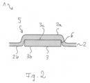
- the Figure 2 shows a multilayer body 1 comprising a substrate 2 and a sensor film 3 in cross section, wherein the first surface 2a of the substrate 2 forms a surface relief 5.
- the surface relief 5 is determined by the shape 6 of the sensor film 3.
- the Figure 1 here the layer sequence 4, which results from the application of the sensor film 3 to the second surface 2b of the substrate 2, wherein the first surface 3a of the sensor film 3 rests on the second surface 2b of the substrate 2.
- a substrate 2 which preferably has a layer thickness, in particular an average layer thickness, between 125 ⁇ m and 3500 ⁇ m, in particular between 400 ⁇ m and 1500 ⁇ m, preferably between 600 ⁇ m and 1100 ⁇ m, before thermoforming.
- a substrate 2 which, after thermoforming, preferably has a layer thickness, in particular an average layer thickness, between 125 ⁇ m and 3500 ⁇ m, in particular between 400 ⁇ m and 1500 ⁇ m, preferably between 600 ⁇ m and 1100 ⁇ m.
- a sensor film 3 which in particular has a layer thickness between 10 ⁇ m and 300 ⁇ m, in particular between 50 ⁇ m and 200 ⁇ m, preferably between 60 ⁇ m and 150 ⁇ m.
- the application of the sensor film 3 to the second surface 2b of the substrate 2 is carried out in particular by means of lamination, wherein the lamination temperature is between 80°C and 300°C, in particular between 100°C and 300°C, preferably between 120°C and 240°C, wherein in particular the lamination speed is between 0.125 m/min and 10 m/min, preferably between 0.25 m/min and 7.5 m/min, particularly preferably between 0.125 m/min and 5 m/min
- Figure 2 the multilayer body 1 after thermoforming of the Figure 1 shown layer sequence 4 comprising the substrate 2 and the sensor film 3 applied to the second surface 2b of the substrate 2, wherein during thermoforming a surface relief 5 is formed on the first surface 2a of the substrate 2, which surface relief is determined by the shape 6 of the sensor film 3.
- the surface relief 5 is formed by deep drawing and heating of the substrate 2, wherein the substrate is preferably heated to a surface temperature between 80°C and 300°C, in particular between 90°C and 250°C, preferably between 100°C and 300°C, wherein in particular the core temperature of the substrate is between 120°C and 160°C, preferably between 100°C and 180°C, particularly preferably between 80°C and 200°C, and/or wherein a pressure, in particular an overpressure between 1 bar and 6 bar, in particular between 2 bar and 5 bar, preferably between 2 bar and 3.5 bar, is applied. This pressure acts on the substrate in particular from one of the two sides.
- a vacuum i.e., a negative pressure
- a negative pressure is preferably applied from the corresponding other substrate side, which is preferably between 0.1 bar and 0.9 bar, in particular between 0.2 bar and 0.8 bar.
- an overpressure can act from the front side of the substrate and a negative pressure from the back side of the substrate, or vice versa; this preferably means that a negative pressure is applied from the front side of the substrate and an overpressure from the back side of the substrate.
- the surface relief 5 is formed by laminating the layer sequence 4, wherein the laminating temperature is preferably between 80°C and 300°C, in particular between 100°C and 260°C, preferably between 120°C and 240°C, wherein in particular the laminating speed is between 0.125 m/min and 10 m/min, preferably between 0.25 m/min and 10 m/min, particularly preferably between 0.5 m/min and 10 m/min, and/or preferably between 0.25 m/min and 7.5 m/min.
- the laminating temperature is preferably between 80°C and 300°C, in particular between 100°C and 260°C, preferably between 120°C and 240°C
- the laminating speed is between 0.125 m/min and 10 m/min, preferably between 0.25 m/min and 10 m/min, particularly preferably between 0.5 m/min and 10 m/min, and/or preferably between 0.25 m/min and 7.5 m/min.
- the multi-layer body 1 may comprise a single-layer or multi-layer substrate 2 having a first surface 2a and a second surface 2b and one or more sensor films 3, each comprising at least one sensor region and having a first surface 3a and a second surface 3b facing away from the first surface 3a, wherein the one or more sensor films 3 are arranged on the second surface 2b of the substrate 2, wherein the first surface 3a of the sensor film 3 rests on the second surface 2b of the substrate 2, and wherein a surface relief 5 is formed on the first surface 2a of the substrate 2, which is determined by the shape 6, in particular contour and/or height relief, of one or more of the one or more sensor films 3.
- a substrate 2 is provided as substrate 2 and/or a sensor film 3 is provided as sensor film 3, which comprise one or more decorative layers, wherein in particular the decorative layers have one or more pictograms in one or more areas, preferably in the sensor area, wherein one or more pictograms of the one or more pictograms overlap or complement each other to form an overall pictogram.
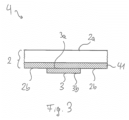
- the Figure 3 shows a layer sequence 4 comprising a sensor film 3 and a substrate 2 in cross section, wherein the substrate 2 has a decorative layer 41.
- the decorative layer 41 is preferably applied to the surface of the substrate 2 facing the sensor film 3 or to the substrate 2 from the side of the second surface 2b of the substrate 2.
- the first surface 3a of the sensor film 3 lies, in particular, in regions on the second surface 2b of the substrate 2.
- the decorative layer 41 has a layer thickness between 0.01 mm and 10 mm, in particular between 0.1 mm and 2.5 mm, preferably between 0.25 mm and 1.25 mm, and/or between 0.1 mm and 10 mm, in particular between 0.25 mm and 2.5 mm, preferably between 0.25 mm and 1.25 mm.
- the sensor film 3 is applied to the second surface of the substrate 2 comprising the decorative layer 41, in particular by means of an embossing process, a rolling process and/or a back-injection process.
- a substrate 2 is preferably provided as substrate 2 which comprises one or more layers selected from: layers comprising pigments, color layers, metal layers, metallized layers, in particular partially metallized layers, transparent layers, translucent layers, opaque layers.
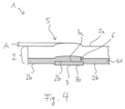
- the Figure 4 shows a multilayer body 1 comprising a substrate 2 in cross section, wherein the substrate 2 has a decorative layer 41 applied to the surface of the substrate 2 facing the sensor film 3, and a sensor film 3, wherein the first surface 2a of the substrate 2 forms a surface relief 5.
- the surface relief 5 is determined by the shape 6 of the sensor film 3.
- the shape 6 of the at least one sensor film 3 is modified when providing the sensor film 3.
- Figure 3 here the layer sequence 4, which results from the application of the sensor film 3 to the second surface 2b of the substrate 2, wherein the first surface 3a of the sensor film 3 rests at least partially on the second surface 2b of the substrate 2.
- Figure 4 the multilayer body 1 after thermoforming of the Figure 3 shown layer sequence 4 comprising the substrate 2 and the sensor film 3 applied to the second surface 2b of the substrate 2, wherein during thermoforming a surface relief 5 is formed on the first surface 2a of the substrate 2, which surface relief is determined by the shape 6 of the sensor film 3.
- the surface relief 5 formed on the first surface 2a of the substrate 2 during thermoforming has a height difference h to the original plane of the first surface 2a of the substrate 2 in the Figure 3 shown layer sequence 4.
- the layers in the Figure 4 The height difference shown is in particular the difference between the absolute maximum of the surface relief 5 and the absolute minimum of the surface relief 5 along a direction which is in particular parallel to the direction defined by the plane of the Figure 4 shown multilayer body 1.
- the absolute minimum of the surface relief 5 corresponds to the plane spanned by the second surface 2a of the substrate 2 outside the surface relief 5.
- the surface relief 5 formed on the first surface 2a of the substrate 2 preferably has a maximum height difference and/or an average height difference between a local minimum of the surface relief 5 or a global minimum of the surface relief 5 and a local maximum of the surface relief 5 or a global maximum of the surface relief 5 that is less than 5000 ⁇ m, in particular less than 2000 ⁇ m, preferably less than 1000 ⁇ m.
- the surface relief 5 formed on the first surface 2a of the substrate 2 to preferably have a maximum height difference and/or an average height difference between a local minimum of the surface relief 5 or a global minimum of the surface relief 5 and a local maximum of the surface relief 5 or a global maximum of the surface relief 5 that is greater than or equal to 50 ⁇ m, in particular greater than 25 ⁇ m, preferably greater than 10 ⁇ m.
- the Figure 5 and Table 1 show the results of a series of measurements as a function of the variables x and y, with the measurement series comprising four measuring points (indicated by squares).
- the variable x corresponds to the layer thickness of the sensor film 3 applied to the substrate 2
- the variable y corresponds to the layer thickness of the substrate 2 after thermoforming.
- Table 1 Layer thickness of substrate before thermoforming Layer thickness of sensor film Height h (especially h shown in Fig. 4 ) y 0 [ ⁇ m] x [ ⁇ m] y 1 [ ⁇ m] 750 98 122 750 170 214 750 250 381 750 500 1150
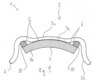
- the Figure 6 shows a multilayer body 1 comprising a sensor film 3 and a substrate 2 in cross-section, wherein the sensor film 3 is applied in regions to the second surface 2b of the substrate 2. Furthermore, a surface relief 5 is formed in the first surface 2a of the substrate 2.
- the multilayer body 1 and in particular the sensor film 3 further have a sensor region 30, which is surrounded in particular by one closed or two non-contiguous edge regions 30'.
- the edge region 30' is arranged in a ring shape, in particular annular, around the sensor region 30, wherein the sensor region 30 is in particular circular in shape.
- the sensor film 3 has one or more sensor elements, in particular capacitive and/or resistive sensor elements, in the sensor region 30. More preferably, the sensor film 3 has a connection region and/or Contact area for contacting, in particular for electrical contacting, one or more of the sensor elements.
- a sensor film 3 which has a base film and one or more electrically conductive layers applied and/or introduced onto the base film, in particular consisting of a metallic material.
- the one or more electrically conductive layers in the sensor region 30 may form one or more sensor electrodes for forming one or more of the sensor elements, in particular for forming one or more capacitive sensor elements and/or one or more resistive sensor elements, and/or for the one or more electrically conductive layers in the connection region and/or contact region to have one or more contact electrodes for contacting the one or more sensor electrodes.
- the sensor region 30 comprises at least one at least partially enclosing edge region, in particular an annular edge region, in particular an annular edge region, in which the one or more sensor electrodes are not present, wherein the edge region preferably encloses the circumference of the sensor region 30 from the outside or from the inside and/or follows the circumference of the sensor region 30 and/or completely or partially overlaps the circumference of the sensor region 30, wherein the edge region preferably has a width, in particular a radial width, between 0.25 mm and 5 mm, preferably between 0.5 mm and 5 mm, and/or that the annular edge region, in particular the annular edge region, preferably has a ring width between 0.25 mm and 5 mm, preferably between 0.5 mm and 2 mm.
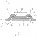
- the Figure 7 shows the Figure 6 shown multilayer body in cross section, except that the present multilayer body 1 has functional elements 33 in the edge regions 30', which are arranged in particular between the second surface 2 of the substrate 2 and the first surface 3a of the sensor film 3.
- the A surface relief 5 is formed on the first surface 2a of the substrate 2, which follows the shape 6.
- the shape 6 is provided in particular by the sensor film 3 and the functional elements 33.
- the shape 6, in particular the contour and/or the relief, of the sensor film 3 to be modified by molding at least one surface relief, wherein the at least one surface relief is molded into one or more layers of the sensor film, in particular by means of one or more methods selected from: thermal replication, UV replication, laser ablation, punching, cutting, embossing, injection molding.
- the surface relief is preferably introduced into the first surface 3a and/or the second surface 3b of the sensor film 3.
- the shape, in particular the height relief and/or the contour, of the sensor film 3 to be modified by applying one or more elements, in particular by applying the functional elements 33, to the base film of the sensor film 3, which are applied in particular by means of one or more of the following methods: printing, in particular printing a varnish and/or by means of 3D printing, laminating a single-layer or multi-layer film element, in particular a plastic label, applying a fabric, in particular glass fiber fabric, applying a fiber material, in particular an organic fiber material, back-injection molding, applying the one or more elements by means of a transfer method, in particular a hot or cold stamping method.
- the functional elements 33 are applied in particular to a first surface of a base film of the sensor film 3, wherein preferably the first surface of the base film faces the first surface 3a of the sensor film 3 and/or partially forms the first surface 3a of the sensor film.
- the functional elements 33 may be applied to one or more of the functional elements 33 applied to the first surface of the base film of the sensor film 3.
- the functional elements 33 can be applied to the base film in the sensor region 30 of the sensor film 3 and to completely or partially overlap the sensor region 30, in particular projected onto the plane spanned by the first surface 3a of the at least one sensor film 3, in particular a flat or curved plane.
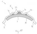
- the Figure 8 shows the Figure 6 shown multilayer body in cross section, except that the present multilayer body 1 has a curvature. Furthermore, the surface relief 5 formed in the first surface 2a of the substrate 2 has a curvature which in particular follows the curvature of the multilayer body 1.
- the layer sequence 4 underlying the multilayer body 1 preferably has a curvature with a minimum or maximum radius of curvature and/or with an average radius of curvature of not less than 1.5 mm, preferably not less than 1 mm, before thermoforming.
- the layer sequence 4 underlying the multilayer body 1 is modified during thermoforming such that the layer sequence 4 after thermoforming or the multilayer body 1 has a curvature with a minimum or maximum radius of curvature and/or with an average radius of curvature of not less than 1.5 mm, preferably not less than 1.0 mm.
- the layer sequence 4 and/or the multi-layer body 1 have different or identical curvatures in different directions.
- the Figure 9 shows the Figure 7 multilayer body shown comprising the elements 33 in cross section, except that the present multilayer body 1 has a curvature. Furthermore, the surface relief 5 formed in the first surface 2a of the substrate 2 has a curvature which in particular follows the curvature of the multilayer body 1 and the shape 6 determined by the sensor film 3 and the functional elements 33.
- the Figure 10 shows the Figure 9 shown curved multilayer body in cross section, except that the present multilayer body 1 does not have functional elements 33 at the edges of the sensor film 3, but rather at different distances from the edges of the sensor film 3. Furthermore, the surface relief 5 formed in the first surface 2a of the substrate 2 has a curvature which in particular follows the curvature of the multilayer body 1 and the shape 6 determined by the sensor film 3 and the functional elements 33.
- the Figure 11 shows the Figure 10 shown curved multilayer body in cross section, except that the present multilayer body 1 has functional elements 33 at the edges of the sensor film 3, has functional elements 33 at different distances from the edges of the sensor film 3 and has light guides 34 which are arranged in particular between the functional elements 33 on the first surface 3a of the sensor film 3. Furthermore, the surface relief 5 formed in the first surface 2a of the substrate 2 has a curvature which follows in particular the curvature of the multilayer body 1 and the shape 6 determined by the sensor film 3, the functional elements 33 and the light guide 34.
- one or more of the functional elements 33 are formed by an element which provides an electrical and/or optical function, in particular is formed by a light guide.
- the Figure 12 shows a sensor film 3 comprising a sensor region 30 and a connection region, which preferably ends in a contact region 37, as well as a first surface 3a and a second surface 3b in cross section. Furthermore, the sensor film 3 has a flat or planar shape 6.
- the sensor film 3 preferably comprises a base film.
- the sensor film 3 has the contact region 37 in particular for contacting, in particular for electrical contacting, one or more sensor elements arranged in the sensor region 30.
- the Figure 13 shows the Figure 12 shown sensor film in cross section, except that the present sensor film 3 has a plastic label 32 lying in the sensor area 30 on the first surface 3a of the sensor film 3.
- the Figure 14 shows the Figure 13 shown sensor film comprising the plastic label 32 in cross section, except that the present sensor film 3 has functional elements 33 applied in the sensor area 30 on the surface of the plastic label 32 facing away from the sensor film 3.
- plastic label 32 and/or the functional elements 33 are applied as elements to the first surface of the base film of the sensor film 3, wherein the first surface of the base film faces the first surface 3a of the sensor film 3 and/or partially forms the first surface 3a of the sensor film 3.
- one or more plastic labels 32 and/or one or more functional elements 33 are applied to the plastic label 32 applied to the first surface of the base film of the sensor film 3 and/or to the functional elements 33 applied to the first surface of the base film of the sensor film.
- plastic label 32 and/or the functional elements 33 can be applied in particular to the base film in the sensor region 30 of the sensor film 3 and to completely or partially overlap the sensor region 30, in particular projected onto the plane spanned by the first surface 3a of the at least one sensor film 3, in particular a flat or curved plane.
- the sensor film 3 has the contact area 37, in particular for contacting one or more sensor elements arranged in the sensor area 30, and that the plastic label 32 and/or the functional elements 33 are applied to the base film in the sensor area 30 of the sensor film 3 and preferably the sensor area 30, in particular projected onto the plane spanned by the first surface 3a of the at least one sensor film 3, in particular a flat or curved plane, completely or partially overlap, but do not overlap the contact area 37 of the sensor film 3.
- the Figure 15 shows the Figure 14 shown sensor film comprising the plastic label 32 and the functional elements 33 in cross section, except that the present sensor film 3 has a functional element 33 and a light guide 34 applied in the sensor area 30 on the surface of the plastic label 32 facing away from the sensor film 3.
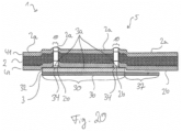
- the Figure 16 shows a substrate 2 comprising two decorative layers 41 in cross section, wherein the two decorative layers 41 are in particular each applied to the substrate 2 from the side of the first surface 2a of the substrate 2 and are applied to the substrate 2 from the side of the second surface 2b of the substrate 2.
- the Figure 17 shows this in the Figure 16 shown substrate 2 comprising two decorative layers 41 and the Figure 13 shown sensor film 3 comprising a plastic label 32 as a layer sequence 4 in cross section, wherein the side of the plastic label 32 facing away from the sensor film 3 rests in regions on the second surface 2b of the substrate 2.
- the Figure 18 shows the Figure 17 shown layer sequence 4 after thermoforming as a multilayer body 1 in cross section, wherein in the first surface 2a of the substrate 2 of the multilayer body 1 a surface relief 5 is formed, which is determined in particular by the shape 6 of the surface of the plastic label 32 facing away from the sensor film 3.
- the Figure 19 shows this in the Figure 14 shown substrate 2 comprising two decorative layers 41 and the Figure 14 shown sensor film 3 comprising a plastic label 32 and the functional elements 33 as a multilayer body 1 after thermoforming in cross section, wherein the side of the plastic label 32 facing away from the sensor film 3 rests partially on the second surface 2b of the substrate 2.
- the Figure 20 shows the Figure 19 shown multilayer body in cross section, except that the present multilayer body 1 or the substrate 2 comprising the two decorative layers 41 has two transparent regions 10.
- the functional elements are preferably designed as light guides 34. Viewed from the first surface 2a of the substrate 2, the emitted light of the light guides 43 can preferably be detected by a viewer through the transparent regions 10 of the substrate 2 comprising the two decorative layers 41.
- the transparent regions 10 are preferably integrated into the surface relief 5 in such a way that the light guides 34 can be detected in particular from the side of the first surface 2a of the substrate 2 of the multilayer body 1.
- the substrate 2 prefferably has one or more transparent regions or the transparent regions 10, wherein in particular the transmittance of the substrate 2 between the first surface 2a of the substrate 2 and the second surface 2b of the substrate 2 in the one or more transparent regions or the transparent regions 10 in a wavelength range visible to the human eye is greater than 1%, preferably greater than 2%, more preferably greater than 4%, and/or less than 99%, preferably less than 95%, more preferably less than 92%.
- the one or more sensor electrodes in particular one or more active sensor regions of the one or more sensor electrodes, which are arranged in particular in the sensor film 3, have a transparency for the human eye with a transmittance of more than 60%, in particular of more than 80%, and/or are each formed by a network of thin conductor tracks with a conductor track width between 3 ⁇ m and 60 ⁇ m, in particular 4 ⁇ m and 60 ⁇ m, particularly preferably between 4 ⁇ m and 50 ⁇ m.
- the surface relief 5 formed on the first surface 2a of the substrate 2 is preferably haptically and/or optically detectable and/or that the surface relief 5 formed on the first surface 2a of the substrate 2 is in particular haptically but not optically detectable or is optically but not haptically detectable or is haptically and not optically detectable or is optically and not haptically detectable.
- the surface relief 5 formed on the first surface of the substrate 2 is formed as Braille, in particular as one or more letters, one or more numbers, one or more words, and/or one or more sentences in Braille.
- the sensor film 3 may have one or more films and/or one or more layers in the sensor region 30, in particular in regions or over the entire surface, selected from: base film, plastic label 32, functional elements 33, in particular light guide 34, decorative layer 41, electrically conductive layer, in particular metallic layer, adhesive layer, adhesion promoter layer, wherein the one or more electrically conductive layers each have one or more sensor electrodes and/or one or more contact electrodes.
- the sensor film 3 it is also possible for the sensor film 3 to have one or more sensor electrodes and/or one or more contact electrodes in the sensor region 30, wherein the sensor electrodes and/or the contact electrodes, in particular projected onto the plane spanned by the first surface 3a of the at least one sensor film 3, in particular a flat or curved plane, are arranged next to one another and/or do not overlap one another and/or, in particular when viewed parallel to a surface normal defined by the plane of the multi-layer body, one or more Sensor electrodes of the one or more sensor electrodes overlap with one or more contact electrodes of the one or more contact electrodes.
- the surface relief 5, in particular projected onto the plane spanned by the first surface 3a of the sensor film 3, in particular a flat or curved plane, is at least partially composed of one or more straight, curved, circular-arc-shaped and/or circular elevations and/or depressions, in particular in the sensor region 30.
- the surface relief 5, in particular projected onto the plane spanned by the first surface 3a of the sensor film 3, in particular a flat or curved plane, is formed at least partially with one or more linear, spiral and/or elliptical elevations and/or depressions, in particular in the sensor region 30.
- the surface relief 5, in particular in the sensor region 30, is formed such that preferably one or more elevations of the one or more elevations and/or one or more depressions of the one or more depressions, in particular in the sensor region 30, each have a constant or varying flank angle and/or a constant or varying width and/or a constant or varying height or depth and/or a constant or varying curvature.
- the shape of one or more elevations of the one or more elevations and/or one or more depressions of the one or more depressions is in each case selected or combined from: line, straight line, motif, image, triangle, wave, square, polygon, curved line, circle, oval, trapezoid, parallelogram, rhombus, cross, sickle, branch structure, star, ellipse, random pattern, pseudo-random pattern, wherein the one or more elevations and/or the one or more depressions in particular overlap and/or complement one another.
- one or more elevations of the one or more elevations and/or one or more depressions of the one or more depressions to be formed over the course, in particular in the plane spanned by the first surface 3a of the sensor film 3, in particular a flat or curved plane, of the respective elevations and/or depressions in such a way that one or more of the heights of the elevations and/or one or more depths of the depressions, in particular perpendicular to the plane spanned by the second surface 2b of the substrate 2, do not have a variation or at least have a variation in sections, wherein the variation is selected from: undulating, symmetrical, asymmetrical, periodic, aperiodic, discrete, continuous, stepped.
Landscapes
- Engineering & Computer Science (AREA)
- Mechanical Engineering (AREA)
- Manufacturing & Machinery (AREA)
- Laminated Bodies (AREA)
- Blow-Moulding Or Thermoforming Of Plastics Or The Like (AREA)
- Lining Or Joining Of Plastics Or The Like (AREA)
Applications Claiming Priority (2)
| Application Number | Priority Date | Filing Date | Title |
|---|---|---|---|
| DE102018124853.9A DE102018124853A1 (de) | 2018-10-09 | 2018-10-09 | Verfahren zur Herstellung eines Mehrschichtkörpers und ein Mehrschichtkörper |
| PCT/EP2019/076456 WO2020074305A1 (de) | 2018-10-09 | 2019-09-30 | Verfahren zur herstellung eines mehrschichtkörpers und ein mehrschichtkörper |
Publications (2)
| Publication Number | Publication Date |
|---|---|
| EP3863830A1 EP3863830A1 (de) | 2021-08-18 |
| EP3863830B1 true EP3863830B1 (de) | 2025-03-26 |
Family
ID=68136380
Family Applications (1)
| Application Number | Title | Priority Date | Filing Date |
|---|---|---|---|
| EP19782547.4A Active EP3863830B1 (de) | 2018-10-09 | 2019-09-30 | Verfahren zur herstellung eines mehrschichtkörpers und ein mehrschichtkörper |
Country Status (8)
| Country | Link |
|---|---|
| US (2) | US12076908B2 (https=) |
| EP (1) | EP3863830B1 (https=) |
| JP (1) | JP7482143B2 (https=) |
| KR (1) | KR102879462B1 (https=) |
| CN (1) | CN113226700A (https=) |
| DE (1) | DE102018124853A1 (https=) |
| HU (1) | HUE070886T2 (https=) |
| WO (1) | WO2020074305A1 (https=) |
Families Citing this family (3)
| Publication number | Priority date | Publication date | Assignee | Title |
|---|---|---|---|---|
| DE102020120754A1 (de) | 2020-08-06 | 2022-02-10 | Leonhard Kurz Stiftung & Co. Kg | Transferfolie, Kunststoffspritzgussteil und Verfahren zu deren Herstellung |
| DE102022117446A1 (de) * | 2022-07-13 | 2024-01-18 | Bayerische Motoren Werke Aktiengesellschaft | Spritzgussbauteil für ein Kraftfahrzeug, Verfahren zur Prüfung eines Spritzgussbauteils, Verfahren zum Herstellen eines Spritzgussbauteils und Kraftfahrzeug |
| FR3159577B1 (fr) * | 2024-02-28 | 2026-02-06 | Smrc Automotive Holdings Netherlands Bv | Dispositif de composant isolant de pièces de garniture intérieure pour véhicule et procédé de réalisation d’un tel dispositif |
Citations (2)
| Publication number | Priority date | Publication date | Assignee | Title |
|---|---|---|---|---|
| US20060104037A1 (en) * | 2004-11-12 | 2006-05-18 | Harris Corporation | Multi-functional structural circuits |
| US20080095988A1 (en) * | 2006-10-18 | 2008-04-24 | 3M Innovative Properties Company | Methods of patterning a deposit metal on a polymeric substrate |
Family Cites Families (20)
| Publication number | Priority date | Publication date | Assignee | Title |
|---|---|---|---|---|
| JPS55112321A (en) * | 1979-02-14 | 1980-08-29 | Kuraray Co | Production of modified yarn |
| FI111881B (fi) * | 2000-06-06 | 2003-09-30 | Rafsec Oy | Älykorttiraina ja menetelmä sen valmistamiseksi |
| US6897390B2 (en) * | 2001-11-20 | 2005-05-24 | Touchsensor Technologies, Llc | Molded/integrated touch switch/control panel assembly and method for making same |
| US6824321B2 (en) * | 2002-09-19 | 2004-11-30 | Siemens Communications, Inc. | Keypad assembly |
| DE20307486U1 (de) * | 2003-05-14 | 2003-10-16 | Woehr Richard Gmbh | Umformverfahren für Design- und/oder Frontfolien aus thermoplastischem oder kalt-reckbarem Kunststoff |
| DE20308525U1 (de) * | 2003-05-30 | 2003-08-07 | Woehr Richard Gmbh | Vollflächige und/oder teilsegmentielle 3-D-gestaltete Mehrschichtenfolie mit Tastkappe und Lichtleitkammer für Punkt und/oder Flächenausleuchtung für Bedien- und/oder Designoberflächen |
| DE102005017170B4 (de) | 2005-04-13 | 2010-07-01 | Ovd Kinegram Ag | Transferfolie, Verfahren zu deren Herstellung sowie Mehrschichtkörper und dessen Verwendung |
| US9829977B2 (en) * | 2008-04-02 | 2017-11-28 | Immersion Corporation | Method and apparatus for providing multi-point haptic feedback texture systems |
| JP2010244772A (ja) * | 2009-04-03 | 2010-10-28 | Sony Corp | 静電容量式タッチ部材及びその製造方法、並びに静電容量式タッチ検出装置 |
| JP2010253857A (ja) | 2009-04-27 | 2010-11-11 | Konan Tokushu Sangyo Kk | オーナメント付熱可塑性樹脂シートの成形方法及び成形用型 |
| DE102009031478A1 (de) | 2009-07-01 | 2011-01-05 | Leonhard Kurz Stiftung & Co. Kg | Mehrschichtkörper |
| EP2322345A1 (de) * | 2009-11-06 | 2011-05-18 | Bayer MaterialScience AG | Schichtverbund mit elektrischen und/oder elektronischen Funktionselementen |
| JP2011121183A (ja) * | 2009-12-08 | 2011-06-23 | Sony Corp | 成形品及びその製造方法 |
| US20110316785A1 (en) * | 2010-06-25 | 2011-12-29 | Murray Hidary | Keypad for hand-held devices with touch screens |
| DE102011111506B4 (de) | 2011-08-31 | 2017-05-18 | Leonhard Kurz Stiftung & Co. Kg | Kunststofffolie und Touchsensor |
| DE102013114276A1 (de) * | 2013-12-18 | 2015-06-18 | Leonhard Kurz Stiftung & Co. Kg | Kunststoffformteil und Verfahren zu dessen Herstellung |
| US9724869B2 (en) * | 2014-12-29 | 2017-08-08 | Tacto Tek Oy | Multilayer structure for accommodating electronics and related method of manufacture |
| DE102015100208A1 (de) * | 2015-01-09 | 2016-07-14 | Leonhard Kurz Stiftung & Co. Kg | Verfahren zur Herstellung eines Verbundartikels sowie ein Verbundartikel |
| WO2017056005A1 (en) * | 2015-09-28 | 2017-04-06 | Sabic Global Technologies B.V. | Integrated transparent conductive films for thermal forming applications |
| JP2022510405A (ja) * | 2018-12-06 | 2022-01-26 | コベストロ・インテレクチュアル・プロパティ・ゲゼルシャフト・ミット・ベシュレンクテル・ハフツング・アンド・コー・カーゲー | ワークピース表面を仕上げるための3dプリントによって機能化された膜領域 |
-
2018
- 2018-10-09 DE DE102018124853.9A patent/DE102018124853A1/de active Pending
-
2019
- 2019-09-30 KR KR1020217013888A patent/KR102879462B1/ko active Active
- 2019-09-30 WO PCT/EP2019/076456 patent/WO2020074305A1/de not_active Ceased
- 2019-09-30 EP EP19782547.4A patent/EP3863830B1/de active Active
- 2019-09-30 CN CN201980075872.5A patent/CN113226700A/zh active Pending
- 2019-09-30 HU HUE19782547A patent/HUE070886T2/hu unknown
- 2019-09-30 US US17/283,080 patent/US12076908B2/en active Active
- 2019-09-30 JP JP2021546047A patent/JP7482143B2/ja active Active
-
2024
- 2024-07-25 US US18/783,660 patent/US20240375341A1/en active Pending
Patent Citations (2)
| Publication number | Priority date | Publication date | Assignee | Title |
|---|---|---|---|---|
| US20060104037A1 (en) * | 2004-11-12 | 2006-05-18 | Harris Corporation | Multi-functional structural circuits |
| US20080095988A1 (en) * | 2006-10-18 | 2008-04-24 | 3M Innovative Properties Company | Methods of patterning a deposit metal on a polymeric substrate |
Also Published As
| Publication number | Publication date |
|---|---|
| JP7482143B2 (ja) | 2024-05-13 |
| JP2022508794A (ja) | 2022-01-19 |
| DE102018124853A1 (de) | 2020-04-09 |
| US12076908B2 (en) | 2024-09-03 |
| US20240375341A1 (en) | 2024-11-14 |
| EP3863830A1 (de) | 2021-08-18 |
| KR20210107623A (ko) | 2021-09-01 |
| CN113226700A (zh) | 2021-08-06 |
| HUE070886T2 (hu) | 2025-07-28 |
| KR102879462B1 (ko) | 2025-11-04 |
| US20210379814A1 (en) | 2021-12-09 |
| WO2020074305A1 (de) | 2020-04-16 |
Similar Documents
| Publication | Publication Date | Title |
|---|---|---|
| EP3863830B1 (de) | Verfahren zur herstellung eines mehrschichtkörpers und ein mehrschichtkörper | |
| US10875222B2 (en) | Plastic moulded part and method for the production thereof | |
| EP3384368B1 (de) | Folie sowie verfahren zur herstellung einer folie | |
| EP3856535B1 (de) | Dekorfolie, verfahren zum dekorieren eines kunststoffformteils sowie kunststoffformteil | |
| EP2556591B1 (de) | Kapazitiver annäherungssensor | |
| EP2923823A1 (de) | Formkörper und Verfahren zu dessen Herstellung | |
| DE102009007779C5 (de) | Verfahren zur Herstellung eines ohne technische Hilfsmittel visuell wahrnehmbaren Sicherheitsmerkmals, Sicherheitsmerkmal für kunststoffbasierendes Wert- oder Sicherheitsdokument sowie Dokument mit wenigstens einem solchen Sicherheitsmerkmal | |
| DE202019005292U1 (de) | Fahrzeugzierteil | |
| DE112014005403B4 (de) | Skalenscheibe mit radialen Linien und Kraftfahrzeug-Anzeigegerät mit Skalenscheibe mit radialen Linien | |
| DE102015121195B4 (de) | Folie sowie Verfahren zur Herstellung einer Folie | |
| DE102019107358A1 (de) | Fahrzeugzierteil | |
| DE112018005570T5 (de) | Formartikel, anzeigevorrichtung einschliesslich des formartikels und verfahren zur herstellung eines formartikels | |
| WO2022180020A1 (de) | Schichtkörper mit dekorationsschicht, verbund aus schichtkörper und formkörper sowie verfahren zur herstellung des schichtkörpers | |
| EP3670135B1 (de) | Kaschierte folie, damit hergestelltes kunststoffbauteil, sowie verfahren und werkzeug dafür | |
| WO2020169615A1 (de) | Mehrschichtkörper sowie verfahren zur herstellung eines mehrschichtkörpers | |
| DE102020105312A1 (de) | Bedienelement mit galvanisierter Oberfläche und kraftsensitiver Sensorik | |
| DE112022001846T5 (de) | Dekorationsfilm zum umspritzen, verfahren zur herstellung eines dekorationsfilms zum umspritzen und verfahren zur herstellung eines harzformprodukts | |
| DE20308525U1 (de) | Vollflächige und/oder teilsegmentielle 3-D-gestaltete Mehrschichtenfolie mit Tastkappe und Lichtleitkammer für Punkt und/oder Flächenausleuchtung für Bedien- und/oder Designoberflächen | |
| DE102023108184A1 (de) | Anzeigeelement mit verbesserter optischer Ankopplung eines holografischen Bildträgers an einen Lichtleiter, zugehöriges Bedienelement sowie zugehörige Anordnung und Montageverfahren | |
| DE102015006395B4 (de) | Verfahren zum Herstellen eines Bauteils für ein Kraftfahrzeug, Bauteil und Kraftfahrzeug |
Legal Events
| Date | Code | Title | Description |
|---|---|---|---|
| STAA | Information on the status of an ep patent application or granted ep patent |
Free format text: STATUS: UNKNOWN |
|
| STAA | Information on the status of an ep patent application or granted ep patent |
Free format text: STATUS: THE INTERNATIONAL PUBLICATION HAS BEEN MADE |
|
| PUAI | Public reference made under article 153(3) epc to a published international application that has entered the european phase |
Free format text: ORIGINAL CODE: 0009012 |
|
| STAA | Information on the status of an ep patent application or granted ep patent |
Free format text: STATUS: REQUEST FOR EXAMINATION WAS MADE |
|
| 17P | Request for examination filed |
Effective date: 20210421 |
|
| AK | Designated contracting states |
Kind code of ref document: A1 Designated state(s): AL AT BE BG CH CY CZ DE DK EE ES FI FR GB GR HR HU IE IS IT LI LT LU LV MC MK MT NL NO PL PT RO RS SE SI SK SM TR |
|
| DAV | Request for validation of the european patent (deleted) | ||
| DAX | Request for extension of the european patent (deleted) | ||
| STAA | Information on the status of an ep patent application or granted ep patent |
Free format text: STATUS: EXAMINATION IS IN PROGRESS |
|
| 17Q | First examination report despatched |
Effective date: 20221031 |
|
| GRAP | Despatch of communication of intention to grant a patent |
Free format text: ORIGINAL CODE: EPIDOSNIGR1 |
|
| STAA | Information on the status of an ep patent application or granted ep patent |
Free format text: STATUS: GRANT OF PATENT IS INTENDED |
|
| INTG | Intention to grant announced |
Effective date: 20240918 |
|
| GRAS | Grant fee paid |
Free format text: ORIGINAL CODE: EPIDOSNIGR3 |
|
| GRAA | (expected) grant |
Free format text: ORIGINAL CODE: 0009210 |
|
| STAA | Information on the status of an ep patent application or granted ep patent |
Free format text: STATUS: THE PATENT HAS BEEN GRANTED |
|
| RIN1 | Information on inventor provided before grant (corrected) |
Inventor name: WIMMER, KARIN Inventor name: HEIDL, STEFANIE Inventor name: ULLMANN, ANDREAS Inventor name: SUESS, CHRISTOPH Inventor name: HEINRICH, MATTHIAS |
|
| AK | Designated contracting states |
Kind code of ref document: B1 Designated state(s): AL AT BE BG CH CY CZ DE DK EE ES FI FR GB GR HR HU IE IS IT LI LT LU LV MC MK MT NL NO PL PT RO RS SE SI SK SM TR |
|
| REG | Reference to a national code |
Ref country code: GB Ref legal event code: FG4D Free format text: NOT ENGLISH |
|
| REG | Reference to a national code |
Ref country code: CH Ref legal event code: EP |
|
| REG | Reference to a national code |
Ref country code: DE Ref legal event code: R096 Ref document number: 502019013126 Country of ref document: DE |
|
| REG | Reference to a national code |
Ref country code: IE Ref legal event code: FG4D Free format text: LANGUAGE OF EP DOCUMENT: GERMAN |
|
| PG25 | Lapsed in a contracting state [announced via postgrant information from national office to epo] |
Ref country code: RS Free format text: LAPSE BECAUSE OF FAILURE TO SUBMIT A TRANSLATION OF THE DESCRIPTION OR TO PAY THE FEE WITHIN THE PRESCRIBED TIME-LIMIT Effective date: 20250626 |
|
| PG25 | Lapsed in a contracting state [announced via postgrant information from national office to epo] |
Ref country code: FI Free format text: LAPSE BECAUSE OF FAILURE TO SUBMIT A TRANSLATION OF THE DESCRIPTION OR TO PAY THE FEE WITHIN THE PRESCRIBED TIME-LIMIT Effective date: 20250326 |
|
| REG | Reference to a national code |
Ref country code: LT Ref legal event code: MG9D |
|
| PG25 | Lapsed in a contracting state [announced via postgrant information from national office to epo] |
Ref country code: NO Free format text: LAPSE BECAUSE OF FAILURE TO SUBMIT A TRANSLATION OF THE DESCRIPTION OR TO PAY THE FEE WITHIN THE PRESCRIBED TIME-LIMIT Effective date: 20250626 |
|
| PG25 | Lapsed in a contracting state [announced via postgrant information from national office to epo] |
Ref country code: HR Free format text: LAPSE BECAUSE OF FAILURE TO SUBMIT A TRANSLATION OF THE DESCRIPTION OR TO PAY THE FEE WITHIN THE PRESCRIBED TIME-LIMIT Effective date: 20250326 |
|
| PG25 | Lapsed in a contracting state [announced via postgrant information from national office to epo] |
Ref country code: LV Free format text: LAPSE BECAUSE OF FAILURE TO SUBMIT A TRANSLATION OF THE DESCRIPTION OR TO PAY THE FEE WITHIN THE PRESCRIBED TIME-LIMIT Effective date: 20250326 |
|
| PG25 | Lapsed in a contracting state [announced via postgrant information from national office to epo] |
Ref country code: GR Free format text: LAPSE BECAUSE OF FAILURE TO SUBMIT A TRANSLATION OF THE DESCRIPTION OR TO PAY THE FEE WITHIN THE PRESCRIBED TIME-LIMIT Effective date: 20250627 Ref country code: BG Free format text: LAPSE BECAUSE OF FAILURE TO SUBMIT A TRANSLATION OF THE DESCRIPTION OR TO PAY THE FEE WITHIN THE PRESCRIBED TIME-LIMIT Effective date: 20250326 |
|
| REG | Reference to a national code |
Ref country code: HU Ref legal event code: AG4A Ref document number: E070886 Country of ref document: HU |
|
| REG | Reference to a national code |
Ref country code: NL Ref legal event code: MP Effective date: 20250326 |
|
| PG25 | Lapsed in a contracting state [announced via postgrant information from national office to epo] |
Ref country code: NL Free format text: LAPSE BECAUSE OF FAILURE TO SUBMIT A TRANSLATION OF THE DESCRIPTION OR TO PAY THE FEE WITHIN THE PRESCRIBED TIME-LIMIT Effective date: 20250326 |
|
| PG25 | Lapsed in a contracting state [announced via postgrant information from national office to epo] |
Ref country code: SE Free format text: LAPSE BECAUSE OF FAILURE TO SUBMIT A TRANSLATION OF THE DESCRIPTION OR TO PAY THE FEE WITHIN THE PRESCRIBED TIME-LIMIT Effective date: 20250326 |
|
| PG25 | Lapsed in a contracting state [announced via postgrant information from national office to epo] |
Ref country code: SM Free format text: LAPSE BECAUSE OF FAILURE TO SUBMIT A TRANSLATION OF THE DESCRIPTION OR TO PAY THE FEE WITHIN THE PRESCRIBED TIME-LIMIT Effective date: 20250326 |
|
| PG25 | Lapsed in a contracting state [announced via postgrant information from national office to epo] |
Ref country code: PT Free format text: LAPSE BECAUSE OF FAILURE TO SUBMIT A TRANSLATION OF THE DESCRIPTION OR TO PAY THE FEE WITHIN THE PRESCRIBED TIME-LIMIT Effective date: 20250728 Ref country code: ES Free format text: LAPSE BECAUSE OF FAILURE TO SUBMIT A TRANSLATION OF THE DESCRIPTION OR TO PAY THE FEE WITHIN THE PRESCRIBED TIME-LIMIT Effective date: 20250326 |
|
| PG25 | Lapsed in a contracting state [announced via postgrant information from national office to epo] |
Ref country code: PL Free format text: LAPSE BECAUSE OF FAILURE TO SUBMIT A TRANSLATION OF THE DESCRIPTION OR TO PAY THE FEE WITHIN THE PRESCRIBED TIME-LIMIT Effective date: 20250326 Ref country code: IT Free format text: LAPSE BECAUSE OF FAILURE TO SUBMIT A TRANSLATION OF THE DESCRIPTION OR TO PAY THE FEE WITHIN THE PRESCRIBED TIME-LIMIT Effective date: 20250326 |
|
| PGFP | Annual fee paid to national office [announced via postgrant information from national office to epo] |
Ref country code: HU Payment date: 20250928 Year of fee payment: 7 |
|
| PGFP | Annual fee paid to national office [announced via postgrant information from national office to epo] |
Ref country code: FR Payment date: 20250925 Year of fee payment: 7 |
|
| PG25 | Lapsed in a contracting state [announced via postgrant information from national office to epo] |
Ref country code: EE Free format text: LAPSE BECAUSE OF FAILURE TO SUBMIT A TRANSLATION OF THE DESCRIPTION OR TO PAY THE FEE WITHIN THE PRESCRIBED TIME-LIMIT Effective date: 20250326 |
|
| PG25 | Lapsed in a contracting state [announced via postgrant information from national office to epo] |
Ref country code: RO Free format text: LAPSE BECAUSE OF FAILURE TO SUBMIT A TRANSLATION OF THE DESCRIPTION OR TO PAY THE FEE WITHIN THE PRESCRIBED TIME-LIMIT Effective date: 20250326 |
|
| PG25 | Lapsed in a contracting state [announced via postgrant information from national office to epo] |
Ref country code: SK Free format text: LAPSE BECAUSE OF FAILURE TO SUBMIT A TRANSLATION OF THE DESCRIPTION OR TO PAY THE FEE WITHIN THE PRESCRIBED TIME-LIMIT Effective date: 20250326 |
|
| PG25 | Lapsed in a contracting state [announced via postgrant information from national office to epo] |
Ref country code: IS Free format text: LAPSE BECAUSE OF FAILURE TO SUBMIT A TRANSLATION OF THE DESCRIPTION OR TO PAY THE FEE WITHIN THE PRESCRIBED TIME-LIMIT Effective date: 20250726 |
|
| REG | Reference to a national code |
Ref country code: DE Ref legal event code: R097 Ref document number: 502019013126 Country of ref document: DE |
|
| PGFP | Annual fee paid to national office [announced via postgrant information from national office to epo] |
Ref country code: DE Payment date: 20250929 Year of fee payment: 7 |
|
| PG25 | Lapsed in a contracting state [announced via postgrant information from national office to epo] |
Ref country code: DK Free format text: LAPSE BECAUSE OF FAILURE TO SUBMIT A TRANSLATION OF THE DESCRIPTION OR TO PAY THE FEE WITHIN THE PRESCRIBED TIME-LIMIT Effective date: 20250326 |
|
| PG25 | Lapsed in a contracting state [announced via postgrant information from national office to epo] |
Ref country code: CZ Free format text: LAPSE BECAUSE OF FAILURE TO SUBMIT A TRANSLATION OF THE DESCRIPTION OR TO PAY THE FEE WITHIN THE PRESCRIBED TIME-LIMIT Effective date: 20250326 |
|
| PLBE | No opposition filed within time limit |
Free format text: ORIGINAL CODE: 0009261 |
|
| STAA | Information on the status of an ep patent application or granted ep patent |
Free format text: STATUS: NO OPPOSITION FILED WITHIN TIME LIMIT |
|
| REG | Reference to a national code |
Ref country code: CH Ref legal event code: L10 Free format text: ST27 STATUS EVENT CODE: U-0-0-L10-L00 (AS PROVIDED BY THE NATIONAL OFFICE) Effective date: 20260211 |
|
| 26N | No opposition filed |
Effective date: 20260105 |