EP3852257A1 - Schaltregler mit treiberleistungsklemme - Google Patents
Schaltregler mit treiberleistungsklemme Download PDFInfo
- Publication number
- EP3852257A1 EP3852257A1 EP20213961.4A EP20213961A EP3852257A1 EP 3852257 A1 EP3852257 A1 EP 3852257A1 EP 20213961 A EP20213961 A EP 20213961A EP 3852257 A1 EP3852257 A1 EP 3852257A1
- Authority
- EP
- European Patent Office
- Prior art keywords
- terminal
- driver
- power
- switching regulator
- power switch
- Prior art date
- Legal status (The legal status is an assumption and is not a legal conclusion. Google has not performed a legal analysis and makes no representation as to the accuracy of the status listed.)
- Withdrawn
Links
- 230000003071 parasitic effect Effects 0.000 claims description 13
- 230000007704 transition Effects 0.000 claims description 11
- 230000004048 modification Effects 0.000 description 3
- 238000012986 modification Methods 0.000 description 3
- 238000007599 discharging Methods 0.000 description 1
- 230000020169 heat generation Effects 0.000 description 1
- 238000004806 packaging method and process Methods 0.000 description 1
- 230000001105 regulatory effect Effects 0.000 description 1
Images


Classifications
-
- H—ELECTRICITY
- H02—GENERATION; CONVERSION OR DISTRIBUTION OF ELECTRIC POWER
- H02M—APPARATUS FOR CONVERSION BETWEEN AC AND AC, BETWEEN AC AND DC, OR BETWEEN DC AND DC, AND FOR USE WITH MAINS OR SIMILAR POWER SUPPLY SYSTEMS; CONVERSION OF DC OR AC INPUT POWER INTO SURGE OUTPUT POWER; CONTROL OR REGULATION THEREOF
- H02M1/00—Details of apparatus for conversion
- H02M1/08—Circuits specially adapted for the generation of control voltages for semiconductor devices incorporated in static converters
-
- H—ELECTRICITY
- H02—GENERATION; CONVERSION OR DISTRIBUTION OF ELECTRIC POWER
- H02M—APPARATUS FOR CONVERSION BETWEEN AC AND AC, BETWEEN AC AND DC, OR BETWEEN DC AND DC, AND FOR USE WITH MAINS OR SIMILAR POWER SUPPLY SYSTEMS; CONVERSION OF DC OR AC INPUT POWER INTO SURGE OUTPUT POWER; CONTROL OR REGULATION THEREOF
- H02M3/00—Conversion of DC power input into DC power output
- H02M3/02—Conversion of DC power input into DC power output without intermediate conversion into AC
- H02M3/04—Conversion of DC power input into DC power output without intermediate conversion into AC by static converters
- H02M3/10—Conversion of DC power input into DC power output without intermediate conversion into AC by static converters using discharge tubes with control electrode or semiconductor devices with control electrode
- H02M3/145—Conversion of DC power input into DC power output without intermediate conversion into AC by static converters using discharge tubes with control electrode or semiconductor devices with control electrode using devices of a triode or transistor type requiring continuous application of a control signal
- H02M3/155—Conversion of DC power input into DC power output without intermediate conversion into AC by static converters using discharge tubes with control electrode or semiconductor devices with control electrode using devices of a triode or transistor type requiring continuous application of a control signal using semiconductor devices only
- H02M3/156—Conversion of DC power input into DC power output without intermediate conversion into AC by static converters using discharge tubes with control electrode or semiconductor devices with control electrode using devices of a triode or transistor type requiring continuous application of a control signal using semiconductor devices only with automatic control of output voltage or current, e.g. switching regulators
- H02M3/158—Conversion of DC power input into DC power output without intermediate conversion into AC by static converters using discharge tubes with control electrode or semiconductor devices with control electrode using devices of a triode or transistor type requiring continuous application of a control signal using semiconductor devices only with automatic control of output voltage or current, e.g. switching regulators including plural semiconductor devices as final control devices for a single load
- H02M3/1582—Buck-boost converters
-
- H—ELECTRICITY
- H02—GENERATION; CONVERSION OR DISTRIBUTION OF ELECTRIC POWER
- H02H—EMERGENCY PROTECTIVE CIRCUIT ARRANGEMENTS
- H02H7/00—Emergency protective circuit arrangements specially adapted for specific types of electric machines or apparatus or for sectionalised protection of cable or line systems, and effecting automatic switching in the event of an undesired change from normal working conditions
- H02H7/10—Emergency protective circuit arrangements specially adapted for specific types of electric machines or apparatus or for sectionalised protection of cable or line systems, and effecting automatic switching in the event of an undesired change from normal working conditions for converters; for rectifiers
-
- H—ELECTRICITY
- H02—GENERATION; CONVERSION OR DISTRIBUTION OF ELECTRIC POWER
- H02M—APPARATUS FOR CONVERSION BETWEEN AC AND AC, BETWEEN AC AND DC, OR BETWEEN DC AND DC, AND FOR USE WITH MAINS OR SIMILAR POWER SUPPLY SYSTEMS; CONVERSION OF DC OR AC INPUT POWER INTO SURGE OUTPUT POWER; CONTROL OR REGULATION THEREOF
- H02M1/00—Details of apparatus for conversion
- H02M1/32—Means for protecting converters other than automatic disconnection
-
- H—ELECTRICITY
- H02—GENERATION; CONVERSION OR DISTRIBUTION OF ELECTRIC POWER
- H02M—APPARATUS FOR CONVERSION BETWEEN AC AND AC, BETWEEN AC AND DC, OR BETWEEN DC AND DC, AND FOR USE WITH MAINS OR SIMILAR POWER SUPPLY SYSTEMS; CONVERSION OF DC OR AC INPUT POWER INTO SURGE OUTPUT POWER; CONTROL OR REGULATION THEREOF
- H02M1/00—Details of apparatus for conversion
- H02M1/32—Means for protecting converters other than automatic disconnection
- H02M1/34—Snubber circuits
-
- H—ELECTRICITY
- H02—GENERATION; CONVERSION OR DISTRIBUTION OF ELECTRIC POWER
- H02M—APPARATUS FOR CONVERSION BETWEEN AC AND AC, BETWEEN AC AND DC, OR BETWEEN DC AND DC, AND FOR USE WITH MAINS OR SIMILAR POWER SUPPLY SYSTEMS; CONVERSION OF DC OR AC INPUT POWER INTO SURGE OUTPUT POWER; CONTROL OR REGULATION THEREOF
- H02M3/00—Conversion of DC power input into DC power output
- H02M3/02—Conversion of DC power input into DC power output without intermediate conversion into AC
- H02M3/04—Conversion of DC power input into DC power output without intermediate conversion into AC by static converters
- H02M3/10—Conversion of DC power input into DC power output without intermediate conversion into AC by static converters using discharge tubes with control electrode or semiconductor devices with control electrode
- H02M3/145—Conversion of DC power input into DC power output without intermediate conversion into AC by static converters using discharge tubes with control electrode or semiconductor devices with control electrode using devices of a triode or transistor type requiring continuous application of a control signal
- H02M3/155—Conversion of DC power input into DC power output without intermediate conversion into AC by static converters using discharge tubes with control electrode or semiconductor devices with control electrode using devices of a triode or transistor type requiring continuous application of a control signal using semiconductor devices only
- H02M3/156—Conversion of DC power input into DC power output without intermediate conversion into AC by static converters using discharge tubes with control electrode or semiconductor devices with control electrode using devices of a triode or transistor type requiring continuous application of a control signal using semiconductor devices only with automatic control of output voltage or current, e.g. switching regulators
- H02M3/158—Conversion of DC power input into DC power output without intermediate conversion into AC by static converters using discharge tubes with control electrode or semiconductor devices with control electrode using devices of a triode or transistor type requiring continuous application of a control signal using semiconductor devices only with automatic control of output voltage or current, e.g. switching regulators including plural semiconductor devices as final control devices for a single load
-
- H—ELECTRICITY
- H02—GENERATION; CONVERSION OR DISTRIBUTION OF ELECTRIC POWER
- H02M—APPARATUS FOR CONVERSION BETWEEN AC AND AC, BETWEEN AC AND DC, OR BETWEEN DC AND DC, AND FOR USE WITH MAINS OR SIMILAR POWER SUPPLY SYSTEMS; CONVERSION OF DC OR AC INPUT POWER INTO SURGE OUTPUT POWER; CONTROL OR REGULATION THEREOF
- H02M3/00—Conversion of DC power input into DC power output
- H02M3/02—Conversion of DC power input into DC power output without intermediate conversion into AC
- H02M3/04—Conversion of DC power input into DC power output without intermediate conversion into AC by static converters
- H02M3/10—Conversion of DC power input into DC power output without intermediate conversion into AC by static converters using discharge tubes with control electrode or semiconductor devices with control electrode
- H02M3/145—Conversion of DC power input into DC power output without intermediate conversion into AC by static converters using discharge tubes with control electrode or semiconductor devices with control electrode using devices of a triode or transistor type requiring continuous application of a control signal
- H02M3/155—Conversion of DC power input into DC power output without intermediate conversion into AC by static converters using discharge tubes with control electrode or semiconductor devices with control electrode using devices of a triode or transistor type requiring continuous application of a control signal using semiconductor devices only
- H02M3/156—Conversion of DC power input into DC power output without intermediate conversion into AC by static converters using discharge tubes with control electrode or semiconductor devices with control electrode using devices of a triode or transistor type requiring continuous application of a control signal using semiconductor devices only with automatic control of output voltage or current, e.g. switching regulators
- H02M3/158—Conversion of DC power input into DC power output without intermediate conversion into AC by static converters using discharge tubes with control electrode or semiconductor devices with control electrode using devices of a triode or transistor type requiring continuous application of a control signal using semiconductor devices only with automatic control of output voltage or current, e.g. switching regulators including plural semiconductor devices as final control devices for a single load
- H02M3/1588—Conversion of DC power input into DC power output without intermediate conversion into AC by static converters using discharge tubes with control electrode or semiconductor devices with control electrode using devices of a triode or transistor type requiring continuous application of a control signal using semiconductor devices only with automatic control of output voltage or current, e.g. switching regulators including plural semiconductor devices as final control devices for a single load comprising at least one synchronous rectifier element
-
- Y—GENERAL TAGGING OF NEW TECHNOLOGICAL DEVELOPMENTS; GENERAL TAGGING OF CROSS-SECTIONAL TECHNOLOGIES SPANNING OVER SEVERAL SECTIONS OF THE IPC; TECHNICAL SUBJECTS COVERED BY FORMER USPC CROSS-REFERENCE ART COLLECTIONS [XRACs] AND DIGESTS
- Y02—TECHNOLOGIES OR APPLICATIONS FOR MITIGATION OR ADAPTATION AGAINST CLIMATE CHANGE
- Y02B—CLIMATE CHANGE MITIGATION TECHNOLOGIES RELATED TO BUILDINGS, e.g. HOUSING, HOUSE APPLIANCES OR RELATED END-USER APPLICATIONS
- Y02B70/00—Technologies for an efficient end-user side electric power management and consumption
- Y02B70/10—Technologies improving the efficiency by using switched-mode power supplies [SMPS], i.e. efficient power electronics conversion e.g. power factor correction or reduction of losses in power supplies or efficient standby modes
Definitions
- the present invention relates to switching regulators.
- a switching regulator is a voltage regulator that uses a switching element to transform the incoming power supply into a regulated output voltage. Power is supplied from the input to the output by turning on and off a power switch (e.g., a MOSFET).
- a power switch e.g., a MOSFET.
- the major advantage of a switching regulator is its higher efficiency compared to standard linear regulators. Lower power dissipation is achieved by internally switching the power switch between an on-state and an off-state. Repeatedly switching the power switch makes it possible to supply voltage efficiently and with less heat generation.
- the switching of the power switch may result in voltage spikes in the circuit.
- Parasitic capacitance and inductance introduced by a printed circuit board (PCB) or other packaging components may cause signal bounce in response to the switching of the power switch.
- Signal bounce includes, for example, ground bounce, supply bounce, and output bounce. Some devices in the circuit may be stressed and perhaps damaged due to the potential difference generated by the signal bounces.
- FIG. 1A depicts a step-down (buck) regulator 102.
- buck step-down
- FIG. 1B depicts a step-up (boost) regulator 104.
- boost boost
- a switching regulator which clamps the power or the ground of the power switch driver is introduced in the present invention and is defined in the claims.
- a buck regulator in accordance with an exemplary embodiment of the present invention comprises a first power switch, an inductor, a diode, a first driver and a driver power clamp.
- the first power switch is coupled between the input terminal of the buck regulator and the first terminal of the inductor.
- the second terminal of the inductor is coupled to the output terminal of the buck regulator.
- the diode is forward biased to provide a current path coupled to the first terminal of the inductor when the first power switch is turned off.
- the first driver is configured to drive the first power switch.
- the driver power clamp is configured to clamp a voltage at a ground terminal of the first driver.
- the driver power clamp comprises a first voltage divider; the first voltage divider has a first resistive element and a second resistive element coupled in series between an internal power supply of the switching regulator and an internal ground of the switching regulator; and the voltage at the ground terminal of the first driver is clamped by a divided voltage at a connection terminal between the first resistive element and the second resistive element.
- the connection terminal between the first resistive element and the second resistive element may be connected to the ground terminal of the first driver during transition intervals while the first driver switches the first power switch from an on-state to an off-state.
- boost regulators are introduced.
- a boost regulator in accordance with an exemplary embodiment of the present invention comprises an inductor, a first power switch, a diode, a first driver, and a driver power clamp.
- the first terminal of the inductor is coupled to the input terminal of the boost regulator, and the first power switch is coupled between the second terminal of the inductor and the negative supply terminal of a power supply.
- the diode is forward biased when the first power switch is turned off to establish a current path between the second terminal of the inductor and an output terminal of the switching regulator.
- the first driver is configured to drive the first power switch.
- the driver power clamp is configured to clamp a voltage at the power terminal of the first driver.
- the driver power clamp comprises a first voltage divider; and the first voltage divider has a first resistive element and a second resistive element coupled in series between a boost terminal of the switching regulator and an internal ground of the switching regulator, and the boost terminal is coupled to the output terminal of the switching regulator; and the voltage at the power terminal of the first driver is clamped by a divided voltage at a connection terminal between the first resistive element and the second resistive element.
- connection terminal between the first resistive element and the second resistive element may be connected to the power terminal of the first driver during transition intervals while the first driver switches the first power switch from an on-state to an off-state.
- the driver power clamp is implemented by a voltage divider and activated during the transition intervals while the first driver switches the first power switch from an on-state to an off-state.
- a switching regulator which clamps the power or the ground of the power switch driver is introduced in the present invention.
- FIG. 2A depicts a step-down (buck) regulator 202 in accordance with an exemplary embodiment of the present invention.
- the buck regulator 202 has a first power switch Mp, a second power switch Mn, an inductor L, a first driver (Mp driver) 204 configured to drive the first power switch Mp, a second driver (Mn driver) 206 configured to drive the second power switch Mn, and a driver power clamp 208 clamping the power of the first driver 204 and clamping the ground of the second driver 206.
- Mp driver first driver
- Mn driver second driver
- driver power clamp 208 clamping the power of the first driver 204 and clamping the ground of the second driver 206.
- the first power switch Mp is coupled between an input terminal Vin of the buck regulator 202 and a first terminal t1 of the inductor L, and a second terminal t2 of the inductor L is coupled to an output terminal Vout of the buck regulator 202.
- the second power switch Mn is coupled between the first terminal t1 of the inductor L and an internal ground Pgnd of the buck regulator 202.
- a body diode 210 of the second power switch Mn When the first power switch Mp is turned on, a body diode 210 of the second power switch Mn is reverse biased. A current flows from the input terminal Vin of the buck regulator 202 to the inductor L to a connected load at the output terminal Vout of the buck regulator 202.
- the body diode 210 of the second power switch Mn When the first power switch Mp is turned off, the body diode 210 of the second power switch Mn is forward biased to establish a current path coupled to the first terminal t1 of the inductor L. Due to the loop established by the current path, the stored energy in the inductor L forces the current to continue flowing through the load in the same direction. A step-down voltage is generated at the output terminal Vout of the buck regulator 202.
- the driver power clamp 208 generates a clamped internal ground Pgnd_clamp to clamp the voltage at a ground terminal 212 of the first driver 204. In this manner, the bounce at the ground terminal 212 of the first driver 204 is controlled within a limited region.
- the first power switch Mp is operated in a safe region and is protected from being damaged by the voltage stress depicted in FIG. 1A . Furthermore, the MOSs in the first driver 204 are protected from being damaged, too.
- the driver power clamp 208 further generates a clamped internal power supply PVDD_clamp to clamp a voltage at a power terminal 214 of the second driver 206.
- the bounce at the power terminal 214 of the second driver 206 is controlled within a limited region.
- the second power switch Mn is also protected by the driver power clamp 208.
- the MOSs in the second driver 206 are protected from being damaged, too.
- the first driver 204 has a power terminal 216 coupled to an internal power supply PVDD of the buck regulator 202.
- the first power switch Mp is a PMOS, having a source biased by the power terminal 216 of the first driver 204, a gate controlled by the first driver 204, and a drain coupled to the first terminal t1 of the inductor L.
- the second driver 206 has a ground terminal 218 coupled to an internal ground Pgnd of the buck regulator 202.
- the second power switch Mn is an NMOS, having a source biased by the ground terminal 218 of the second driver 206, a gate controlled by the second driver 206, and a drain coupled to the first terminal t1 of the inductor L.
- first parasitic inductor Lp1 between the input terminal Vin of the buck regulator 202 and the internal power supply PVDD, and a second parasitic inductor Lp2 between the internal ground Pgnd and a negative supply terminal VSS of a power supply.
- first parasitic inductor Lp1 between the input terminal Vin of the buck regulator 202 and the internal power supply PVDD
- second parasitic inductor Lp2 between the internal ground Pgnd and a negative supply terminal VSS of a power supply.
- the second power switch Mn of the buck regulator 202 is replaced by a diode.
- the diode is reverse biased when the first power switch Mp is turned on and is forward biased when the first power switch Mp is turned off.
- FIG. 2B depicts a step-up (boost) regulator 222 in accordance with an exemplary embodiment of the present invention.
- the boost regulator 222 has a first power switch Mn, a second power switch Mp, an inductor L, a first driver (Mn driver) 224 configured to drive the first power switch Mn, a second driver (Mp driver) 226 configured to drive the second power switch Mp, and a driver power clamp 228 clamping the power of the first driver 224 and clamping the ground of the second driver 226.
- Mn driver first driver
- Mp driver second driver
- driver power clamp 228 clamping the power of the first driver 224 and clamping the ground of the second driver 226.
- An input terminal Vin of the boost regulator 222 is coupled to a first terminal t1 of the inductor L, and the first power switch Mn is coupled between a second terminal t2 of the inductor L and a negative supply terminal VSS of a power supply.
- the boost regulator 202 further has an internal boost terminal Vboost (at a boost voltage also labeled Vboost).
- the driver power clamp 228 generates a clamped boost voltage Vboost_clamp to clamp a voltage at a power terminal 232 of the first driver 224. In this manner, the bounce at the power terminal 232 of the first driver 224 is controlled within a limited region.
- the first power switch Mn is operated in a safe region and is protected from being damaged by the voltage stress depicted in FIG. 1B . Furthermore, the MOSs in the first driver 224 are protected from being damaged, too.
- the driver power clamp 228 further generates a clamped internal ground Pgnd_clamp to clamp a voltage at a ground terminal 234 of the second driver 226.
- Pgnd_clamp a clamped internal ground
- the second power switch Mp is also protected by the driver power clamp 228.
- the MOSs in the second driver 226 are protected from being damaged, too.
- the first driver 224 has a ground terminal 236 coupled to an internal ground Pgnd of the boost regulator 222.
- the first power switch Mn is an NMOS, having a source biased by the ground terminal 236 of the first driver 224, a gate controlled by the first driver 224, and a drain coupled to the second terminal t2 of the inductor L.
- the second driver 226 has a power terminal 238 that is the internal boost terminal Vboost coupled to the output terminal Vout of the boost regulator 222.
- the second power switch Mp is a PMOS, having a source biased by the power terminal 238 of the second driver 226, a gate controlled by the second driver 226, and a drain coupled to the second terminal t2 of the inductor L.
- the second power switch Mp of the boost regulator 222 is replaced by a diode.
- the diode is reverse biased when the first power switch Mn is turned on and is forward biased when the first power switch Mn is turned off.
- FIG. 3 depicts the clamped internal power supply PVDD_clamp (or the clamped boost voltage Vboost_clamp) and the clamped internal ground Pgnd_clamp generated by the driver power clamp 208/228.
- the driver power clamp 208/228 is powered by the internal power supply PVDD (or the boost voltage Vboost) and is grounded to the internal ground Pgnd.
- the bounces at the internal power supply PVDD or the bounces at the boost voltage Vboost
- the bounces at the internal ground Pgnd are effectively clamped.
- the clamped internal power supply PVDD_clamp (or the clamped boost voltage Vboost_clamp) and the clamped internal ground Pgnd clamp are applied to the power switch drivers to protect the power switches Mp and Mn and the MOSs of the power switch driver from being damaged.
- FIG. 4A depicts the timing of driver power clamping of the buck regulator 202 in accordance with an exemplary embodiment of the present invention.
- the driver power clamp 208 is activated during transition intervals while the first driver 204 switches the first power switch Mp from an on-state to an off-state.
- FIG. 4B depicts the timing of driver power clamping of the boost regulator 222 in accordance with an exemplary embodiment of the present invention.
- the driver power clamp 228 is activated during transition intervals while the first driver 224 switches the first power switch Mn from an on-state to an off-state.
- the driver power clamp 208/228 is implemented by voltage dividers.
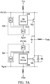
- FIG. 5A depicts a first voltage divider 502 and a second voltage 504 for driver power clamping of the buck regulator 202.
- the first voltage divider 502 has a first resistive element R1 and a second resistive element R2 coupled in series between the internal power supply PVDD of the buck regulator 202 and the internal ground Pgnd of the buck regulator 202.
- the voltage at the ground terminal 212 of the first driver 204 is clamped by a divided voltage at a connection terminal between the first resistive element R1 and the second resistive element R2.
- the second voltage divider 504 has a third resistive element R3 and a fourth resistive element R4 coupled in series between the internal power supply PVDD of the buck regulator 202 and the internal ground Pgnd of the buck regulator 202.
- the voltage at the power terminal 214 of the second driver 206 is clamped by a divided voltage at a connection terminal between the third resistive element R3 and the fourth resistive element R4. It should be noted that the driver power clamping shown in FIG. 5A is performed during transition intervals while the first driver 204 switches the first power switch Mp from an on-state to an off-state.
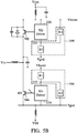
- FIG. 5B depicts a first voltage divider 506 and a second voltage 508 for driver power clamping of the boost regulator 222.
- the first voltage divider 506 has a first resistive element R1 and a second resistive element R2 coupled in series between the boost voltage Vboost and the internal ground Pgnd of the boost regulator 222.
- the voltage at the power terminal 232 of the first driver 224 is clamped by a divided voltage at a connection terminal between the first resistive element R1 and the second resistive element R2.
- the second voltage divider 508 has a third resistive element R3 and a fourth resistive element R4 coupled in series between the boost voltage Vboost and the internal ground Pgnd of the boost regulator 222.
- the voltage at the ground terminal 234 of the second driver 226 is clamped by a divided voltage at a connection terminal between the third resistive element R3 and the fourth resistive element R4. It should be noted that the driver power clamping shown in FIG. 5B is performed during transition intervals while the first driver 224 switches the first power switch Mn from an on-state to an off-state.
Landscapes
- Engineering & Computer Science (AREA)
- Power Engineering (AREA)
- Dc-Dc Converters (AREA)
- Control Of Eletrric Generators (AREA)
- Air Bags (AREA)
Applications Claiming Priority (2)
| Application Number | Priority Date | Filing Date | Title |
|---|---|---|---|
| US202062961941P | 2020-01-16 | 2020-01-16 | |
| US17/092,425 US11522439B2 (en) | 2020-01-16 | 2020-11-09 | Switching regulator with driver power clamp |
Publications (1)
| Publication Number | Publication Date |
|---|---|
| EP3852257A1 true EP3852257A1 (de) | 2021-07-21 |
Family
ID=73838891
Family Applications (1)
| Application Number | Title | Priority Date | Filing Date |
|---|---|---|---|
| EP20213961.4A Withdrawn EP3852257A1 (de) | 2020-01-16 | 2020-12-14 | Schaltregler mit treiberleistungsklemme |
Country Status (4)
| Country | Link |
|---|---|
| US (2) | US11522439B2 (de) |
| EP (1) | EP3852257A1 (de) |
| CN (1) | CN113141112B (de) |
| TW (1) | TWI771816B (de) |
Families Citing this family (2)
| Publication number | Priority date | Publication date | Assignee | Title |
|---|---|---|---|---|
| US11522439B2 (en) * | 2020-01-16 | 2022-12-06 | Mediatek Inc. | Switching regulator with driver power clamp |
| CN121689819A (zh) * | 2026-02-06 | 2026-03-17 | 英彼森半导体(珠海)有限公司 | 一种具有钳位功能的电源管理电路 |
Citations (3)
| Publication number | Priority date | Publication date | Assignee | Title |
|---|---|---|---|---|
| US5793245A (en) * | 1996-10-15 | 1998-08-11 | Texas Instruments Incorporated | Wide range gate-source clamp |
| US9673812B2 (en) * | 2013-06-04 | 2017-06-06 | Panasonic Intellectual Property Management Co., Ltd. | Gate driver and power module equipped with same |
| US9831867B1 (en) * | 2016-02-22 | 2017-11-28 | Navitas Semiconductor, Inc. | Half bridge driver circuits |
Family Cites Families (18)
| Publication number | Priority date | Publication date | Assignee | Title |
|---|---|---|---|---|
| US3261105A (en) | 1962-10-29 | 1966-07-19 | Phillips Petroleum Co | Drying ammonium nitrate prills |
| CN2529453Y (zh) * | 2002-03-20 | 2003-01-01 | 威盛电子股份有限公司 | 可降低电源/接地弹跳噪声的输出缓冲器 |
| TW200525867A (en) * | 2004-01-21 | 2005-08-01 | Renesas Tech Corp | Voltage clamp circuit, switching power supply apparatus, semiconductor IC device, and voltage level converting circuit |
| US7075343B2 (en) * | 2004-12-07 | 2006-07-11 | Analog Devices, Inc. | Self-timed switching regulator pre-driver |
| US20070170897A1 (en) * | 2006-01-26 | 2007-07-26 | Advanced Analogic Technologies, Inc. | High-Frequency Power MESFET Buck Switching Power Supply |
| US7852125B2 (en) * | 2006-05-29 | 2010-12-14 | Koninklijke Philips Electronics N.V. | Switching circuit arrangement |
| TWI381618B (zh) | 2008-12-22 | 2013-01-01 | Asustek Comp Inc | 交換式電源電路及電腦系統 |
| JP4803262B2 (ja) * | 2009-01-27 | 2011-10-26 | 株式会社村田製作所 | 絶縁型スイッチング電源装置 |
| CN103151930A (zh) * | 2013-04-02 | 2013-06-12 | 上海新时达电气股份有限公司 | 开关电源 |
| US9035687B2 (en) * | 2013-10-09 | 2015-05-19 | Infineon Technologies Ag | Gate clamping |
| CN105099151A (zh) | 2014-04-18 | 2015-11-25 | 台达电子企业管理(上海)有限公司 | 变换器 |
| US9343949B2 (en) | 2014-09-22 | 2016-05-17 | Texas Instruments Incorporated | Control circuit to detect a noise signal during a state change of a switch |
| US9712055B1 (en) * | 2015-10-21 | 2017-07-18 | Picor Corporation | Zero voltage switching energy recovery control of discontinuous PWM switching power converters |
| US9837903B2 (en) * | 2015-12-31 | 2017-12-05 | Stmicroelectronics S.R.L. | Method to recover from current loop instability after cycle by cycle current limit intervention in peak current mode control |
| US10784763B2 (en) | 2017-03-07 | 2020-09-22 | Mediatek Inc. | Dynamic slew rate control |
| CN106953510B (zh) | 2017-03-23 | 2019-05-10 | 上海英联电子系统有限公司 | 开关器件电压尖峰有源钳位自驱动电路 |
| FR3088779B1 (fr) * | 2018-11-20 | 2020-12-04 | Commissariat Energie Atomique | Circuit d’alimentation de circuits de commande d’interrupteurs |
| US11522439B2 (en) * | 2020-01-16 | 2022-12-06 | Mediatek Inc. | Switching regulator with driver power clamp |
-
2020
- 2020-11-09 US US17/092,425 patent/US11522439B2/en active Active
- 2020-11-30 CN CN202011381387.1A patent/CN113141112B/zh active Active
- 2020-12-02 TW TW109142373A patent/TWI771816B/zh active
- 2020-12-14 EP EP20213961.4A patent/EP3852257A1/de not_active Withdrawn
-
2022
- 2022-11-08 US US18/053,417 patent/US11742743B2/en active Active
Patent Citations (3)
| Publication number | Priority date | Publication date | Assignee | Title |
|---|---|---|---|---|
| US5793245A (en) * | 1996-10-15 | 1998-08-11 | Texas Instruments Incorporated | Wide range gate-source clamp |
| US9673812B2 (en) * | 2013-06-04 | 2017-06-06 | Panasonic Intellectual Property Management Co., Ltd. | Gate driver and power module equipped with same |
| US9831867B1 (en) * | 2016-02-22 | 2017-11-28 | Navitas Semiconductor, Inc. | Half bridge driver circuits |
Also Published As
| Publication number | Publication date |
|---|---|
| CN113141112A (zh) | 2021-07-20 |
| US11742743B2 (en) | 2023-08-29 |
| TW202129452A (zh) | 2021-08-01 |
| US20230065722A1 (en) | 2023-03-02 |
| US20210226524A1 (en) | 2021-07-22 |
| TWI771816B (zh) | 2022-07-21 |
| CN113141112B (zh) | 2025-01-17 |
| US11522439B2 (en) | 2022-12-06 |
Similar Documents
| Publication | Publication Date | Title |
|---|---|---|
| US11831245B2 (en) | Switching control device, driving device, isolated DC-DC converter, AC-DC converter, power adapter, and electric appliance | |
| CN110022068B (zh) | 具有有源钳位器的同步整流栅极驱动器 | |
| US7791371B2 (en) | Level shift circuit and power semiconductor device | |
| US20110043955A1 (en) | Electrostatic discharge protection circuit, control method therefor, and switching regulator using same | |
| KR20010014888A (ko) | 스위칭 레귤레이터 | |
| US11588410B2 (en) | Switched mode power supplies with configurable communication addresses | |
| US11742743B2 (en) | Switching regulator with driver power clamp | |
| US11005382B2 (en) | Synchronous rectification controlling device, isolated synchronous-rectification DC-DC converter, gate driving device, isolated DC-DC converter, AC-DC converter, power adapter, and electric appliance | |
| CN113767557A (zh) | 具有自举电路的有源箝位 | |
| US10103633B1 (en) | Switching converter with power level selection | |
| US9306464B2 (en) | Synchronous rectifier control circuits of power converters | |
| KR20190064963A (ko) | Dc-dc 변환 시스템 | |
| US10008922B2 (en) | Switching power supply | |
| CN100547895C (zh) | 用于同步整流dc-dc转换器的负脉冲消除器电路和方法 | |
| US8072186B2 (en) | USB charger circuit | |
| JP7568502B2 (ja) | スイッチング電源用回路及びスイッチング電源装置 | |
| CN221428779U (zh) | Dc-dc转换器 | |
| US7538530B2 (en) | Buck converter | |
| KR100429131B1 (ko) | 보조 출력 전압 공급을 위한 전력 공급 시스템 | |
| JP4328417B2 (ja) | 電源回路 | |
| JP5569786B2 (ja) | Dc−dcコンバータ | |
| JP3514600B2 (ja) | スイッチング電源及びその制御方法 | |
| CN114189151A (zh) | Dc-dc升压变换器 | |
| US20250357846A1 (en) | Dc/dc converter operable efficiently while preventing reverse current | |
| JP2977482B2 (ja) | 自励式dc−dcコンバータ |
Legal Events
| Date | Code | Title | Description |
|---|---|---|---|
| PUAI | Public reference made under article 153(3) epc to a published international application that has entered the european phase |
Free format text: ORIGINAL CODE: 0009012 |
|
| STAA | Information on the status of an ep patent application or granted ep patent |
Free format text: STATUS: THE APPLICATION HAS BEEN PUBLISHED |
|
| AK | Designated contracting states |
Kind code of ref document: A1 Designated state(s): AL AT BE BG CH CY CZ DE DK EE ES FI FR GB GR HR HU IE IS IT LI LT LU LV MC MK MT NL NO PL PT RO RS SE SI SK SM TR |
|
| STAA | Information on the status of an ep patent application or granted ep patent |
Free format text: STATUS: REQUEST FOR EXAMINATION WAS MADE |
|
| 17P | Request for examination filed |
Effective date: 20220121 |
|
| RBV | Designated contracting states (corrected) |
Designated state(s): AL AT BE BG CH CY CZ DE DK EE ES FI FR GB GR HR HU IE IS IT LI LT LU LV MC MK MT NL NO PL PT RO RS SE SI SK SM TR |
|
| STAA | Information on the status of an ep patent application or granted ep patent |
Free format text: STATUS: EXAMINATION IS IN PROGRESS |
|
| 17Q | First examination report despatched |
Effective date: 20230316 |
|
| P01 | Opt-out of the competence of the unified patent court (upc) registered |
Effective date: 20230607 |
|
| STAA | Information on the status of an ep patent application or granted ep patent |
Free format text: STATUS: THE APPLICATION HAS BEEN WITHDRAWN |
|
| 18W | Application withdrawn |
Effective date: 20240126 |