EP3851906B1 - Hintergrundbeleuchtungsmodul, anzeigebildschirm und mobiles endgerät - Google Patents
Hintergrundbeleuchtungsmodul, anzeigebildschirm und mobiles endgerät Download PDFInfo
- Publication number
- EP3851906B1 EP3851906B1 EP19930209.2A EP19930209A EP3851906B1 EP 3851906 B1 EP3851906 B1 EP 3851906B1 EP 19930209 A EP19930209 A EP 19930209A EP 3851906 B1 EP3851906 B1 EP 3851906B1
- Authority
- EP
- European Patent Office
- Prior art keywords
- light
- layer
- light source
- disposed
- backlight module
- Prior art date
- Legal status (The legal status is an assumption and is not a legal conclusion. Google has not performed a legal analysis and makes no representation as to the accuracy of the status listed.)
- Active
Links
Images

Classifications
-
- G—PHYSICS
- G02—OPTICS
- G02B—OPTICAL ELEMENTS, SYSTEMS OR APPARATUS
- G02B5/00—Optical elements other than lenses
- G02B5/02—Diffusing elements; Afocal elements
- G02B5/0205—Diffusing elements; Afocal elements characterised by the diffusing properties
- G02B5/021—Diffusing elements; Afocal elements characterised by the diffusing properties the diffusion taking place at the element's surface, e.g. by means of surface roughening or microprismatic structures
- G02B5/0231—Diffusing elements; Afocal elements characterised by the diffusing properties the diffusion taking place at the element's surface, e.g. by means of surface roughening or microprismatic structures the surface having microprismatic or micropyramidal shape
-
- G—PHYSICS
- G02—OPTICS
- G02B—OPTICAL ELEMENTS, SYSTEMS OR APPARATUS
- G02B6/00—Light guides; Structural details of arrangements comprising light guides and other optical elements, e.g. couplings
- G02B6/0001—Light guides; Structural details of arrangements comprising light guides and other optical elements, e.g. couplings specially adapted for lighting devices or systems
- G02B6/0011—Light guides; Structural details of arrangements comprising light guides and other optical elements, e.g. couplings specially adapted for lighting devices or systems the light guides being planar or of plate-like form
- G02B6/0033—Means for improving the coupling-out of light from the light guide
- G02B6/005—Means for improving the coupling-out of light from the light guide provided by one optical element, or plurality thereof, placed on the light output side of the light guide
- G02B6/0055—Reflecting element, sheet or layer
-
- G—PHYSICS
- G02—OPTICS
- G02B—OPTICAL ELEMENTS, SYSTEMS OR APPARATUS
- G02B5/00—Optical elements other than lenses
- G02B5/02—Diffusing elements; Afocal elements
- G02B5/0205—Diffusing elements; Afocal elements characterised by the diffusing properties
- G02B5/0236—Diffusing elements; Afocal elements characterised by the diffusing properties the diffusion taking place within the volume of the element
- G02B5/0242—Diffusing elements; Afocal elements characterised by the diffusing properties the diffusion taking place within the volume of the element by means of dispersed particles
-
- G—PHYSICS
- G02—OPTICS
- G02B—OPTICAL ELEMENTS, SYSTEMS OR APPARATUS
- G02B6/00—Light guides; Structural details of arrangements comprising light guides and other optical elements, e.g. couplings
- G02B6/0001—Light guides; Structural details of arrangements comprising light guides and other optical elements, e.g. couplings specially adapted for lighting devices or systems
- G02B6/0011—Light guides; Structural details of arrangements comprising light guides and other optical elements, e.g. couplings specially adapted for lighting devices or systems the light guides being planar or of plate-like form
- G02B6/0013—Means for improving the coupling-in of light from the light source into the light guide
- G02B6/0023—Means for improving the coupling-in of light from the light source into the light guide provided by one optical element, or plurality thereof, placed between the light guide and the light source, or around the light source
- G02B6/0031—Reflecting element, sheet or layer
-
- G—PHYSICS
- G02—OPTICS
- G02B—OPTICAL ELEMENTS, SYSTEMS OR APPARATUS
- G02B6/00—Light guides; Structural details of arrangements comprising light guides and other optical elements, e.g. couplings
- G02B6/0001—Light guides; Structural details of arrangements comprising light guides and other optical elements, e.g. couplings specially adapted for lighting devices or systems
- G02B6/0011—Light guides; Structural details of arrangements comprising light guides and other optical elements, e.g. couplings specially adapted for lighting devices or systems the light guides being planar or of plate-like form
- G02B6/0033—Means for improving the coupling-out of light from the light guide
- G02B6/005—Means for improving the coupling-out of light from the light guide provided by one optical element, or plurality thereof, placed on the light output side of the light guide
- G02B6/0051—Diffusing sheet or layer
-
- G—PHYSICS
- G02—OPTICS
- G02B—OPTICAL ELEMENTS, SYSTEMS OR APPARATUS
- G02B6/00—Light guides; Structural details of arrangements comprising light guides and other optical elements, e.g. couplings
- G02B6/0001—Light guides; Structural details of arrangements comprising light guides and other optical elements, e.g. couplings specially adapted for lighting devices or systems
- G02B6/0011—Light guides; Structural details of arrangements comprising light guides and other optical elements, e.g. couplings specially adapted for lighting devices or systems the light guides being planar or of plate-like form
- G02B6/0033—Means for improving the coupling-out of light from the light guide
- G02B6/005—Means for improving the coupling-out of light from the light guide provided by one optical element, or plurality thereof, placed on the light output side of the light guide
- G02B6/0053—Prismatic sheet or layer; Brightness enhancement element, sheet or layer
-
- G—PHYSICS
- G02—OPTICS
- G02B—OPTICAL ELEMENTS, SYSTEMS OR APPARATUS
- G02B6/00—Light guides; Structural details of arrangements comprising light guides and other optical elements, e.g. couplings
- G02B6/0001—Light guides; Structural details of arrangements comprising light guides and other optical elements, e.g. couplings specially adapted for lighting devices or systems
- G02B6/0011—Light guides; Structural details of arrangements comprising light guides and other optical elements, e.g. couplings specially adapted for lighting devices or systems the light guides being planar or of plate-like form
- G02B6/0065—Manufacturing aspects; Material aspects
-
- G—PHYSICS
- G02—OPTICS
- G02F—OPTICAL DEVICES OR ARRANGEMENTS FOR THE CONTROL OF LIGHT BY MODIFICATION OF THE OPTICAL PROPERTIES OF THE MEDIA OF THE ELEMENTS INVOLVED THEREIN; NON-LINEAR OPTICS; FREQUENCY-CHANGING OF LIGHT; OPTICAL LOGIC ELEMENTS; OPTICAL ANALOGUE/DIGITAL CONVERTERS
- G02F1/00—Devices or arrangements for the control of the intensity, colour, phase, polarisation or direction of light arriving from an independent light source, e.g. switching, gating or modulating; Non-linear optics
- G02F1/01—Devices or arrangements for the control of the intensity, colour, phase, polarisation or direction of light arriving from an independent light source, e.g. switching, gating or modulating; Non-linear optics for the control of the intensity, phase, polarisation or colour
- G02F1/13—Devices or arrangements for the control of the intensity, colour, phase, polarisation or direction of light arriving from an independent light source, e.g. switching, gating or modulating; Non-linear optics for the control of the intensity, phase, polarisation or colour based on liquid crystals, e.g. single liquid crystal display cells
- G02F1/133—Constructional arrangements; Operation of liquid crystal cells; Circuit arrangements
- G02F1/1333—Constructional arrangements; Manufacturing methods
- G02F1/1335—Structural association of cells with optical devices, e.g. polarisers or reflectors
- G02F1/133528—Polarisers
- G02F1/133531—Polarisers characterised by the arrangement of polariser or analyser axes
-
- G—PHYSICS
- G02—OPTICS
- G02F—OPTICAL DEVICES OR ARRANGEMENTS FOR THE CONTROL OF LIGHT BY MODIFICATION OF THE OPTICAL PROPERTIES OF THE MEDIA OF THE ELEMENTS INVOLVED THEREIN; NON-LINEAR OPTICS; FREQUENCY-CHANGING OF LIGHT; OPTICAL LOGIC ELEMENTS; OPTICAL ANALOGUE/DIGITAL CONVERTERS
- G02F1/00—Devices or arrangements for the control of the intensity, colour, phase, polarisation or direction of light arriving from an independent light source, e.g. switching, gating or modulating; Non-linear optics
- G02F1/01—Devices or arrangements for the control of the intensity, colour, phase, polarisation or direction of light arriving from an independent light source, e.g. switching, gating or modulating; Non-linear optics for the control of the intensity, phase, polarisation or colour
- G02F1/13—Devices or arrangements for the control of the intensity, colour, phase, polarisation or direction of light arriving from an independent light source, e.g. switching, gating or modulating; Non-linear optics for the control of the intensity, phase, polarisation or colour based on liquid crystals, e.g. single liquid crystal display cells
- G02F1/133—Constructional arrangements; Operation of liquid crystal cells; Circuit arrangements
- G02F1/1333—Constructional arrangements; Manufacturing methods
- G02F1/1335—Structural association of cells with optical devices, e.g. polarisers or reflectors
- G02F1/1336—Illuminating devices
- G02F1/133602—Direct backlight
- G02F1/133603—Direct backlight with LEDs
-
- G—PHYSICS
- G02—OPTICS
- G02F—OPTICAL DEVICES OR ARRANGEMENTS FOR THE CONTROL OF LIGHT BY MODIFICATION OF THE OPTICAL PROPERTIES OF THE MEDIA OF THE ELEMENTS INVOLVED THEREIN; NON-LINEAR OPTICS; FREQUENCY-CHANGING OF LIGHT; OPTICAL LOGIC ELEMENTS; OPTICAL ANALOGUE/DIGITAL CONVERTERS
- G02F1/00—Devices or arrangements for the control of the intensity, colour, phase, polarisation or direction of light arriving from an independent light source, e.g. switching, gating or modulating; Non-linear optics
- G02F1/01—Devices or arrangements for the control of the intensity, colour, phase, polarisation or direction of light arriving from an independent light source, e.g. switching, gating or modulating; Non-linear optics for the control of the intensity, phase, polarisation or colour
- G02F1/13—Devices or arrangements for the control of the intensity, colour, phase, polarisation or direction of light arriving from an independent light source, e.g. switching, gating or modulating; Non-linear optics for the control of the intensity, phase, polarisation or colour based on liquid crystals, e.g. single liquid crystal display cells
- G02F1/133—Constructional arrangements; Operation of liquid crystal cells; Circuit arrangements
- G02F1/1333—Constructional arrangements; Manufacturing methods
- G02F1/1335—Structural association of cells with optical devices, e.g. polarisers or reflectors
- G02F1/1336—Illuminating devices
- G02F1/133602—Direct backlight
- G02F1/133605—Direct backlight including specially adapted reflectors
-
- G—PHYSICS
- G02—OPTICS
- G02F—OPTICAL DEVICES OR ARRANGEMENTS FOR THE CONTROL OF LIGHT BY MODIFICATION OF THE OPTICAL PROPERTIES OF THE MEDIA OF THE ELEMENTS INVOLVED THEREIN; NON-LINEAR OPTICS; FREQUENCY-CHANGING OF LIGHT; OPTICAL LOGIC ELEMENTS; OPTICAL ANALOGUE/DIGITAL CONVERTERS
- G02F1/00—Devices or arrangements for the control of the intensity, colour, phase, polarisation or direction of light arriving from an independent light source, e.g. switching, gating or modulating; Non-linear optics
- G02F1/01—Devices or arrangements for the control of the intensity, colour, phase, polarisation or direction of light arriving from an independent light source, e.g. switching, gating or modulating; Non-linear optics for the control of the intensity, phase, polarisation or colour
- G02F1/13—Devices or arrangements for the control of the intensity, colour, phase, polarisation or direction of light arriving from an independent light source, e.g. switching, gating or modulating; Non-linear optics for the control of the intensity, phase, polarisation or colour based on liquid crystals, e.g. single liquid crystal display cells
- G02F1/133—Constructional arrangements; Operation of liquid crystal cells; Circuit arrangements
- G02F1/1333—Constructional arrangements; Manufacturing methods
- G02F1/1335—Structural association of cells with optical devices, e.g. polarisers or reflectors
- G02F1/1336—Illuminating devices
- G02F1/133602—Direct backlight
- G02F1/133606—Direct backlight including a specially adapted diffusing, scattering or light controlling members
-
- G—PHYSICS
- G02—OPTICS
- G02F—OPTICAL DEVICES OR ARRANGEMENTS FOR THE CONTROL OF LIGHT BY MODIFICATION OF THE OPTICAL PROPERTIES OF THE MEDIA OF THE ELEMENTS INVOLVED THEREIN; NON-LINEAR OPTICS; FREQUENCY-CHANGING OF LIGHT; OPTICAL LOGIC ELEMENTS; OPTICAL ANALOGUE/DIGITAL CONVERTERS
- G02F1/00—Devices or arrangements for the control of the intensity, colour, phase, polarisation or direction of light arriving from an independent light source, e.g. switching, gating or modulating; Non-linear optics
- G02F1/01—Devices or arrangements for the control of the intensity, colour, phase, polarisation or direction of light arriving from an independent light source, e.g. switching, gating or modulating; Non-linear optics for the control of the intensity, phase, polarisation or colour
- G02F1/13—Devices or arrangements for the control of the intensity, colour, phase, polarisation or direction of light arriving from an independent light source, e.g. switching, gating or modulating; Non-linear optics for the control of the intensity, phase, polarisation or colour based on liquid crystals, e.g. single liquid crystal display cells
- G02F1/133—Constructional arrangements; Operation of liquid crystal cells; Circuit arrangements
- G02F1/1333—Constructional arrangements; Manufacturing methods
- G02F1/1335—Structural association of cells with optical devices, e.g. polarisers or reflectors
- G02F1/1336—Illuminating devices
- G02F1/133602—Direct backlight
- G02F1/133606—Direct backlight including a specially adapted diffusing, scattering or light controlling members
- G02F1/133607—Direct backlight including a specially adapted diffusing, scattering or light controlling members the light controlling member including light directing or refracting elements, e.g. prisms or lenses
Definitions
- This application relates to the field of mobile terminal technologies, and in particular, to a backlight module, a display, and a mobile terminal.
- a liquid crystal display When a liquid crystal display works, a liquid crystal material itself does not emit light, and needs to rely on a passive light source. The light source needs to illuminate a liquid crystal panel from the back, and light output is controlled to form an image.
- an LED Light Emitting Diode, light emitting diode
- a side-emitting type structure or a direct-emitting type structure is usually used.
- a light source is disposed on a side of a module.
- Light rays enter from the side and pass through a light guide plate.
- the light rays propagate inside a waveguide with a limitation by a waveguide function.
- the light rays are uniformly coupled and emitted gradually by using scattering dots, to form a surface light source.
- This solution has advantages of being light and thin.
- all LED light sources need to be always turned on to ensure uniform light output, and light emitting of the LED light sources cannot be adjusted based on brightness of an image region.
- light sources are disposed directly below a panel and uniformly arranged in an array. Light rays are shed directly on a display panel from below, to form uniform illumination on the display panel.
- a main characteristic of this structure is that light emitting brightness of a light source in a corresponding region may be controlled point by point based on brightness of a displayed image, to reduce power consumption and improve image contrast.
- the direct-emitting type backlight structure uses a point light source, brightness in a vertical direction is much greater than that in a surrounding region, and a relatively long light mixture distance is required to change the point light source into a surface light source. Therefore, the direct-emitting type backlight structure is usually used in a large-size product insensitive to a thickness such as a television and is difficult to be made thin, and therefore cannot be applied to a scenario such as a mobile phone display that needs to be highly thin.
- the document US 2019/137825 A1 shows a backlight unit and liquid crystal display device including the backlight unit. Especially, a repeated reflection of light emitted by light sources between layers of the backlight unit is shown.
- the document KR 2009 0073452 A shows a liquid crystal display comprising a trenched light guide plate with a light-emitting diode array in the trench.
- the document US 2019/129249 A1 shows a liquid crystal display device comprising a liquid crystal panel and a backlight unit under the liquid crystal panel.
- the document US 2018/059482 A1 shows a display comprising an array of pixels and a backlight for illuminating the array of pixels, where the backlight comprises a two-dimensional array of light-emitting diodes.
- the document WO 2018/116815 A1 shows a light guiding plate comprising a scattering portion to scatter light emitted from a light-emitting element, and a limiting portion to block light going toward outside.
- the document US 2018/335559 A1 shows a backlight unit comprising a light guide panel with a concaved light receiving region and means for light intensity adjustment opposite to the concaved region.
- This application provides a backlight module, a display, and a mobile terminal, to reduce a light mixture distance in a backlight structure.
- a backlight module mainly includes three parts: a backplane having a light reflecting surface, a light source layer disposed on the light reflecting surface, and at least one light mixing component disposed on the light source layer.
- the light source layer has at least one point light source, and the at least one light mixing component is in a one-to-one correspondence with the at least one point light source.
- Each light mixing component includes a light reflecting layer configured to reflect some light rays emitted by a corresponding point light source, and a light transmission layer configured to transmit a light ray reflected by the light reflecting layer and then reflected again by the light reflecting surface.
- the light reflecting layer is disposed above the light source layer and is configured to reflect the some light rays emitted by the corresponding point light source.
- the light reflecting layer reflects the some light rays emitted by the point light source, and the some light rays are reflected again by the light reflecting surface on the backplane and then emitted from the light transmission layer. In this way, the light rays are more uniformly emitted from the backlight module, and a light mixture distance of the backlight structure is reduced.
- a light diffusion structure is disposed on at least one of a light input surface and a light output surface of the light transmission layer, to improve light output uniformity of the light transmission layer.
- the light diffusion structure is a concave-convex structure disposed on the light input surface or the light output surface, to facilitate disposing.
- a shape of the concave-convex structure may be specifically a jagged shape, to facilitate disposing and improve light output uniformity of the light transmission layer.
- scattering particles are provided in the light transmission layer, to improve light output uniformity of the light transmission layer.
- the light reflecting layer is disposed on a surface that is on the light source layer and that is away from the backplane.
- the light reflecting layer is a light reflecting coating covering the surface that is on the light source layer and that is away from the backplane, to facilitate disposing of the light reflecting layer.
- a vertical distance between the light reflecting layer and the light reflecting surface gradually increases in a direction away from the point light source, so that more light rays emitted by the point light source are emitted from a region away from the point light source, thereby improving a light mixing effect.
- the light output surface of the light transmission layer is a convex or concave surface, so that a light ray is emitted from the light transmission layer.
- each light mixing component further includes at least one column that is disposed on the light reflecting layer or the light transmission layer and that can reflect light, to form an air layer used for light mixing above the light transmission layer and the light reflecting layer, thereby improving a light mixing effect.
- an area of a cross section of each of the at least one column gradually decreases in a direction away from the light reflecting surface, to prevent the column from affecting light mixing.
- the backlight module further includes a substrate that is disposed on the light source layer and that can transmit light, the light reflecting layer is disposed on a surface that is on the substrate and that is away from the light source layer, and the light transmission layer is a part of the substrate that is not covered by the light reflecting layer.
- the light mixing component is first disposed on the substrate, and then the substrate is disposed on the light source layer, to improve an overall yield rate.
- a plurality of through holes that can transmit light are provided on the light reflecting layer, so that some light rays are output from the through holes on the light reflecting layer, thereby improving a light mixing effect.
- the backlight module further includes a protective layer for encapsulating the light reflecting layer, to protect the backlight module.
- the backlight module further includes a light guide layer disposed on the at least one light mixing component.
- the light transmission layer is a plurality of gluing layers disposed between the light guide layer and the light source layer, and the plurality of gluing layers are arranged at intervals to form an air layer between adjacent gluing layers.
- the light reflecting layer is the air layer.
- the air layer is used as the light reflecting layer, so that the some light rays emitted by the point light source may be emitted from the air layer, and after being reflected, the some light rays are reflected at least once and are emitted from the gluing layer, thereby improving a light mixing effect.
- an area of each of the plurality of gluing layers gradually increases from a position close to the corresponding point light source to a position that is away from the corresponding point light source, so that more light rays are emitted from an edge region of the point light source, thereby improving a light mixing effect.
- the light guide layer includes a prism film bonded to the plurality of gluing layers and a diffusion film disposed on the prism film, to improve a light mixing effect.
- the light reflecting surface is a diffuse reflecting surface or a specular reflecting surface with a high reflectivity, to improve reflecting efficiency of the reflecting surface.
- a display includes any one of the foregoing backlight modules, that are according to the claims, a polarizer stacked on a side that is of the backlight module and that is away from a backplane, and a display layer stacked on the polarizer, to improve a light mixing effect of the display and reduce a thickness of the display.
- the display further includes a cover plate stacked on a side that is of the display and that is away from the polarizer, to protect the display layer.
- a mobile terminal includes a frame and any one of the foregoing displays disposed on the frame, to improve a light mixing effect of the display of the mobile terminal and reduce a thickness of the display.
- the backlight module is applied to a display of a mobile terminal such as a mobile phone or a computer.
- a mobile terminal such as a mobile phone or a computer.
- the backlight module mainly includes three parts based on functions.
- the three parts are: a backplane having a light reflecting surface, a light source layer disposed on the light reflecting surface, and at least one light mixing component disposed on the light source layer.
- the backplane 10 is a board structure.
- the backplane 10 may be a printed circuit board, or may be a board structure disposed on a printed circuit board.
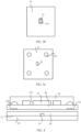
- the backplane 10 includes an upper surface and a lower surface that are opposite to each other (referring to the backlight module shown in FIG. 1 ), where the upper surface of the backplane 10 is a light reflecting surface 11.
- the light reflecting surface 11 is disposed, the light reflecting surface 11 is a diffuse reflecting surface or a specular reflecting surface with a high reflectivity.
- the high reflectivity is specifically any value that is greater than 0.80 and less than 1.0, such as 0.80, 0.82, 0.85, 0.87, 0.90, 0.92, 0.95, 0.97, and 1.0.
- a coating with a high reflectivity may cover a surface of the board structure, to form the light reflecting surface 11 that can reflect light on the surface of the board structure.
- an array of the plurality of point light sources 21 is arranged on the light reflecting surface 11 of the backplane 10. It should be understood that an arrangement manner of the plurality of point light sources 21 is not limited to the disposing manner of the foregoing array arrangement, and another disposing manner may be used.
- the light source layer 20 further has an encapsulating material for encapsulating the at least one point light source 21.
- the encapsulating material may be silica gel, or may be another conventional encapsulating material that can transmit light, to protect the point light source 21.
- the encapsulating material does not affect light ray output of the point light source 21.
- phosphor may be mixed into the encapsulating material, to change a color of light emitted by the point light source 21. It should be understood that a disposing manner of the light source layer 20 is not limited to the foregoing disposing manner. In addition, another disposing manner may be used.
- the at least one light mixing component is disposed on the light source layer 20, and the at least one light mixing component is in a one-to-one correspondence with the at least one point light source 21.
- a quantity of light mixing components is equal to that of point light sources 21, and each light mixing component corresponds to one point light source 21.
- Each light mixing component is disposed in a region above a corresponding point light source 21 and a region between two adjacent point light sources 21, to mix light of the point light sources 21.
- Each light mixing component includes a light reflecting layer 31 configured to reflect some light rays emitted by a corresponding point light source 21, and a light transmission layer 32 configured to transmit a light ray reflected by the light reflecting layer 31 and then reflected again by the light reflecting surface 11.
- the light reflecting layer 31 is disposed right above the corresponding point light source 21 or in a region approximately right above the point light source 21.
- the light transmission layer 32 is disposed in an edge region of the corresponding point light source 21.
- the light transmission layer 32 is disposed in a region between adjacent point light sources 21.
- the light reflecting layer 31 is disposed above the light source layer 20 and is configured to reflect the some light rays emitted by the corresponding point light source 21.
- the light reflecting layer 31 reflects the some light rays emitted by the point light source 21, and the some light rays are reflected again by the light reflecting surface 11 on the backplane 10 and then emitted from the light transmission layer 32. In this way, the light rays are more uniformly emitted from the backlight module.
- the light reflecting layer 31 is disposed on a surface that is on the light source layer 20 and that is away from the backplane 10.
- the light transmission layer 32 is a part of the light source layer 20 that is not covered by the light reflecting layer 31.
- the light reflecting layer 31 may be a conventional light reflecting board that can reflect light in the prior art, and the light reflecting board may be disposed on the light source layer 20 in a bonding manner.
- a disposing manner of the light reflecting layer 31 is not limited to the foregoing disposing manner of using the light reflecting board.
- another disposing manner may be used. For example, referring to FIG.
- the light reflecting layer 31 may be a light reflecting coating covering the surface that is on the light source layer 20 and that is away from the backplane 10, to facilitate disposing.
- a material of the light reflecting coating is a material that can reflect light and is easy to coat in the prior art. Referring to FIG. 1 , the light reflecting layer 31 is disposed in a region right above and a region diagonally above the corresponding point light source 21 (the backlight module shown in FIG. 1 is used as a reference), so that a coverage area of the light reflecting layer 31 is greater than that of the point light source 21. Referring to FIG.
- a light input surface of the light reflecting layer 31 may be a plane parallel to or approximately parallel to the light reflecting surface 11, to simplify disposing.
- the light input surface of the light reflecting layer 31 may also be an arc-shaped surface that curves inwards.
- a vertical distance between the light reflecting layer 31 and the light reflecting surface 11 gradually increases in a direction away from the point light source 21, so that the light ray emitted by the point light source 21 is transmitted to a position that is away from the point light source 21 after being reflected by the light reflecting layer 31 and the light reflecting surface 11 for a plurality of times, and more light rays emitted by the point light source 21 are emitted from a region away from the point light source 21, to improve a light mixing effect.
- a shape of the light reflecting surface 11 is not limited to the foregoing disposing manner, and another disposing manner may be used.
- the light reflecting layer 31 may be a complete structure without a through hole.
- a through hole 311 that can transmit light is disposed on the light reflecting layer 31.
- two elliptic through holes 311 are disposed on the light reflecting layer 31.
- one elliptic through hole 311 is disposed on the light reflecting layer 31, and a center of the through hole 311 coincides with that of a corresponding point light source 21.
- a quantity of through holes 311 is not limited to that used in the foregoing disposing manner, and may be specifically any value of at least one of one, two, three, or the like.
- a shape of the through hole 311 is not limited to the foregoing elliptical or circular disposing manner.
- the shape of the through hole 311 may be any shape such as a triangle or a rectangle.
- a disposing position of the through hole 311 is not limited to the foregoing disposing manner in which the center of the through hole 311 coincides with that of the point light source 21, and the through hole 311 may be disposed at another position.
- the disposing position of the through hole 311 is not limited to the foregoing disposing manner of surrounding the point light source 21, and another arrangement manner may be alternatively used.
- a plurality of through holes 311 are arranged on the light reflecting layer 31 in an unordered manner.
- the unordered manner is all manners that help uniformly emit a light ray.
- the through hole 311 is disposed on the light reflecting layer 31, so that some light rays on the point light source 21 are emitted from the through hole 311, thereby reducing light ray intensity above the point light source 21 and making the light ray intensity above the point light source 21 more uniform.
- the light transmission layer 32 is a part of the light source layer 20.
- the light output surface of the light transmission layer 32 is a surface that is on the light source layer 20 and that is away from the backplane 10
- the light input surface of the light transmission layer 32 is a surface that faces the backplane 10.
- the light output surface of the light transmission layer 32 may be a plane, to simplify disposing. Referring to FIG.
- the light output surface of the light transmission layer 32 may further be a convex or concave surface, that is, a vertical distance between the light output surface of the light transmission layer 32 and the light reflecting surface 11 of the backplane 10 gradually changes in a direction away from the point light source 21, to form the convex or concave surface, so that a light ray is emitted from the light transmission layer 32.
- the light transmission layer 32 can directly emit, from the light transmission layer 32, the some light rays emitted by the point light source 21.
- a light ray reflected by the light reflecting layer 31 is reflected by the light reflecting surface 11 and then emitted from the light transmission layer 32.
- disposing manners of the light input surface and the light output surface of the light transmission layer 32 is not limited to the foregoing disposing manners, and another disposing manner may be used.
- a light diffusion structure 321 is disposed on at least one of the light input surface and the light output surface of the light transmission layer 32.
- the light diffusion structure 321 is a concave-convex structure disposed on the light output surface of the light transmission layer 32.
- the concave-convex structure may be a spherical protrusion disposed on the light output surface of the light transmission layer 32, or may be a jagged concave-convex structure, so that the light rays are more uniformly emitted from the light transmission layer 32.
- the light diffusion structure 321 is not limited to the foregoing disposing manner, and another conventional disposing manner that can help light diffusion in the prior art may be used. FIG. 1 and FIG. 2 only show that the light diffusion structure 321 is disposed on the light output surface of the light transmission layer 32.
- the light diffusion structure 321 may be alternatively disposed on the light input surface of the light transmission layer 32.
- the disposing manner of disposing the light diffusion structure 321 on at least one of the light input surface or the light output surface of the light transmission layer 32 falls within the protection scope of the embodiments of this application.
- scattering particles 322 may be further disposed in the light transmission layer 32.
- the scattering particles 322 are specifically conventional scattering particles 322 that can help light ray scattering in the prior art.
- the scattering particles 322 may be disposed in the light transmission layer 32.
- all the scattering particles 322 may be arranged in the light transmission layer 32.
- some scattering particles 322 may be embedded in the light transmission layer 32, and some scattering particles 322 are exposed outside the light transmission layer 32.
- the scattering particles 322 are disposed in the light transmission layer 32, so that light output uniformity of the light transmission layer 32 can be improved.
- the light reflecting layer 31 is further encapsulated by a protective layer 50, to protect the backlight module.
- a material of the protective layer 50 is a light transmission material. Specifically, a silica gel material may be selected.
- phosphor may be mixed into the protective layer 50, to change a color of the light ray emitted by the point light source 21.
- At least one column 33 that can reflect light may be further disposed on the light reflecting layer 31 or the light transmission layer 32, to form an air layer used for light mixing above the light transmission layer 32 and the light reflecting layer 31.
- the column 33 may be disposed on the light reflecting layer 31.
- the column 33 may be alternatively disposed on the light transmission layer 32.
- the column 33 may be disposed on the light reflecting surface 11 of the backplane 10, and one end of the column 33 is exposed outside the light transmission layer 32.
- a material of the column 33 may be a conventional light transmission material in the prior art, to prevent the column 33 from affecting a light mixing effect.
- a surface of the column 33 may be coated with a material that can reflect light, to improve a light mixing effect.
- a material that can reflect light Referring to FIG. 2 , an area of a cross section of each column 33 gradually decreases in a direction away from the light reflecting surface 11, that is, a lower end of the column 33 is larger and an upper end of the column 33 is smaller (refer to the backlight module shown in FIG. 2 ).
- the column 33 may be a cone structure, or may be a tapered prism structure. A structure with a larger lower end and a smaller upper end is used as the column 33, to prevent the column 33 from affecting light mixing.
- the two or more columns 33 may be arranged around the point light source 21.
- a polarizer or another layer structure is stacked on the backlight module, because the column 33 supports the layer structure, an air layer that can be used for light mixing is provided above the light mixing component, thereby improving a light mixing effect. It should be understood that the foregoing shows only one disposing manner of the column 33, and another disposing manner may be used.
- the backlight module further includes a substrate 40 that is disposed on the light source layer 20 and that can transmit light, and the light reflecting layer 31 is disposed on a surface that is on the substrate 40 and that is away from the light source layer 20.
- the light transmission layer 32 is a part of the substrate 40 that is not covered by the light reflecting layer 31.
- a material of the substrate 40 may be specifically PET (Polyethylene terephthalate, polyethylene terephthalate).
- a disposing manner of the light reflecting layer 31 is basically the same as the foregoing disposing manner, except that a disposing position is different.
- the light reflecting layer 31 is disposed on a side that is of the substrate 40 and that is away from the light source layer 20.
- a disposing manner of the light transmission layer 32 is basically the same as the foregoing disposing manner, except that composition of the light transmission layer 32 is different.
- the light transmission layer 32 is a part of the substrate 40 that is not covered by the light reflecting layer 31.
- the light input surface of the light transmission layer 32 is a surface that is on the substrate 40 and that faces the light source layer 20.
- the light output surface of the light transmission layer 32 is the surface that is on the substrate 40 and that is away from the light source layer 20.
- the light diffusion structure 321 is disposed on both the light input surface and the light output surface of the light transmission layer 32, to improve light ray output uniformity.
- the light mixing component is first disposed on the substrate 40, and then the substrate 40 is disposed on the light source layer 20, to prevent a processing failure of the light mixing component from affecting reuse of the light source layer 20, thereby improving an overall yield rate.
- a backlight layer and the light transmission layer 32 are disposed in another manner.
- the backlight module further includes a light guide layer 60 disposed on the at least one light mixing component.
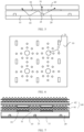
- the light transmission layer 32 is a plurality of gluing layers disposed between the light guide layer 60 and the light source layer 20, and the plurality of gluing layers are arranged at intervals to form an air layer between adjacent gluing layers.
- the light reflecting layer 31 is the air layer.
- a refraction angle of a light ray becomes smaller when the light ray is propagated from an optically denser medium to an optically thinner medium, total reflection of the light occurs, so that the some light rays emitted by the point light source 21 are reflected from the air layer. Because a difference between a density of the gluing layer and densities of the light source layer 20 and the light guide layer 60 is less than a difference between a density of air and the densities of the light source layer 20 and the light guide layer 60, it is easier to emit a light ray from the gluing layer than to emit light from the air layer.
- the light reflected by the air layer is reflected by the light reflecting surface 11 on the backplane 10, and then may be emitted by using the gluing layer, so that a light mixing effect can be improved by controlling a disposing position of the gluing layer.
- the light reflecting layer 31 may be disposed in an upper region of each point light source 21, or may be disposed in a region between two adjacent point light sources 21.
- a material of the gluing layer is specifically a material that can transmit light in the prior art, for example, may be an OCA optically clear adhesive (Optically Clear Adhesive, which is a special adhesive used to bond a transparent optical element).
- OCA optically clear Adhesive which is a special adhesive used to bond a transparent optical element.
- There may be specifically at least 2, such as 2, 4, 8, 12, 16, gluing layers.
- a shape of each gluing layer may be specifically a circle shown in FIG. 6 , or may be another shape such as an ellipse, a rectangle, or a triangle.
- the plurality of gluing layers may be arranged in an arrangement manner of an array shown in FIG. 6 , or may be arranged in another manner. Areas of all the plurality of gluing layers may be equal or not equal. Referring to FIG. 6 , an area of each of the plurality of gluing layers gradually increases from a position close to the corresponding point light source 21 to a position that is away from the corresponding point light source 21, so that more light rays are emitted from an edge region of the point light source 21, thereby improving a light mixing effect. It should be understood that the foregoing shows only several disposing manners of the gluing layer, and another disposing manner may be used.
- the light diffusion structure 321 may be disposed on a surface that is on the gluing layer and that is bonded to the light guide layer 60.
- the light diffusion structure 321 may be disposed on a surface that is on the gluing layer and that is bonded to the light source layer 20.
- the manner of disposing the light diffusion structure 321 on either or both of the surface that is on the gluing layer and that is bonded to the light guide layer 60 or the surface that is on the gluing layer and that is bonded to the light source layer 20 falls within the protection scope of this embodiment of this application.
- the light diffusion structure 321 is disposed on the gluing layer, to improve a light mixing effect.
- the scattering particles 322 may be further disposed in the gluing layer. During specific processing, the scattering particles 322 may be doped into a gluing material, to improve a light mixing effect.
- the light guide layer 60 When the light guide layer 60 is disposed, referring to FIG. 7 , the light guide layer 60 includes a prism film 61 bonded to a plurality of gluing layers and a diffusion film 62 disposed on the prism film 61. There may be one prism film 61, or there may be two or more prism films 61. When there are two prism films 61, the two prism films 61 are stacked together in different directions. Prisms on the two prism films 61 may be extended in a perpendicular manner, to improve a brightness enhancement effect. Referring to FIG. 7 , one layer of diffusion film 62 is disposed on the prism film 61, and the diffusion film 62 is a conventional film that can perform light diffusion in the prior art. Still referring to FIG.
- a plurality of gluing layers are also disposed between the prism film 61 and the diffusion film 62, to improve a light mixing effect.
- Two layers of prism films 61 that extend in perpendicular directions may be further disposed on the diffusion film 62, to improve brightness of a light ray emitted by the backlight module.
- the light reflecting layer 31 is disposed above the light source layer 20 and is configured to reflect the some light rays emitted by the corresponding point light source 21.
- the light reflecting layer 31 reflects the some light rays emitted by the point light source 21, and the light rays are reflected again by the light reflecting surface 11 on the backplane 10 and then emitted from the light transmission layer 32. In this way, the light rays are more uniformly emitted from the backlight module, and a light mixture distance of a backlight structure is reduced.
- this application further provides a display.
- the display includes any one of the foregoing backlight modules, that are according to the claimed invention, a polarizer stacked on a side that is of the backlight module and that is away from a backplane, and a display layer stacked on the polarizer, to improve a light mixing effect of the display and reduce a thickness of the display.
- the display further includes a cover plate stacked on a side that is on the display and that is away from the polarizer, to protect the display layer.
- this application further provides a mobile terminal.
- the mobile terminal includes a frame and any one of the foregoing displays disposed on the frame, to improve a light mixing effect of the display of the mobile terminal and reduce a thickness of the display.
Landscapes
- Physics & Mathematics (AREA)
- General Physics & Mathematics (AREA)
- Optics & Photonics (AREA)
- Nonlinear Science (AREA)
- Chemical & Material Sciences (AREA)
- Mathematical Physics (AREA)
- Crystallography & Structural Chemistry (AREA)
- Dispersion Chemistry (AREA)
- Engineering & Computer Science (AREA)
- Manufacturing & Machinery (AREA)
- Planar Illumination Modules (AREA)
Claims (6)
- Hintergrundbeleuchtungsmodul, Folgendes umfassend:eine Rückplatte (10), die eine lichtreflektierende Oberfläche (11) aufweist;eine Lichtquellenschicht (20), die auf der lichtreflektierenden Oberfläche (11) angeordnet ist, wobei die Lichtquellenschicht (20) mindestens eine Punktlichtquelle (21) aufweist;eine Lichtmischkomponente, die auf der Lichtquellenschicht (20) in einer Eins-zu-Eins-Übereinstimmung mit der mindestens einen Punktlichtquelle (21) angeordnet ist; undeine Lichleiterschicht, die auf der mindestens einen Lichtmischkomponente angeordnet ist, wobeijede Lichtmischkomponente eine lichtreflektierende Schicht (31), die dazu konfiguriert ist, einige durch eine entsprechende Punktlichtquelle (21) emittierte Lichtstrahlen zu reflektieren, und eine Lichdurchlässigkeitsschicht (32) umfasst, die dazu konfiguriert ist, einen durch die lichtreflektierende Schicht (31) reflektierten und dann erneut durch die lichtreflektierende Oberfläche (11) reflektierten Lichtstrahl durchzulassen,wobei eine Lichtdiffusionsstruktur (321) auf mindestens einer von einer Lichteintrittsfläche und einer Lichtaustrittsfläche der Lichdurchlässigkeitsschicht (32) angeordnet ist,wobei die Lichtdiffusionsstruktur (321) eine konkav-konvexe Struktur ist, die auf der Lichteintrittsfläche oder der Lichtaustrittsfläche angeordnet ist, undwobei die Lichdurchlässigkeitsschicht (32) eine Vielzahl von Klebeschichten ist, die zwischen der Lichleiterschicht und der Lichtquellenschicht (20) angeordnet ist, und die Vielzahl von Klebeschichten in Abständen in einer Richtung parallel zu der Ebene des Hintergrundbeleuchtungsmoduls angeordnet ist, um eine Luftschicht zwischen benachbarten Klebeschichten zu bilden; und die lichtreflektierende Schicht (31) die Luftschicht ist.
- Hintergrundbeleuchtungsmodul gemäß einem der Ansprüche 1, wobei Streupartikel in der Lichdurchlässigkeitsschicht (32) angeordnet sind.
- Hintergrundbeleuchtungsmodul gemäß einem der Ansprüche 1 oder 2, wobei die lichtreflektierende Schicht (31) auf einer Seite der Lichtquellenschicht (20) angeordnet ist, die von der Rückplatte (10) entfernt ist.
- Hintergrundbeleuchtungsmodul gemäß Anspruch 1, wobei ein Bereich der Vielzahl von Klebeschichten von einer Position nahe der entsprechenden Punktlichtquelle (21) zu einer Position, die von der entsprechenden Punktlichtquelle (21) entfernt ist, allmählich zunimmt.
- Anzeige, umfassend das Hintergrundbeleuchtungsmodul gemäß einem der Ansprüche 1 bis 4, einen Polarisator, der auf einer Seite des Hintergrundbeleuchtungsmoduls gestapelt ist, die von einer Rückplatte (10) entfernt ist, und eine Anzeigeschicht, die auf dem Polarisator gestapelt ist.
- Mobiles Endgerät, umfassend einen Rahmen und die Anzeige gemäß Anspruch 5, die auf dem Rahmen angeordnet ist.
Applications Claiming Priority (2)
| Application Number | Priority Date | Filing Date | Title |
|---|---|---|---|
| CN201920805599.4U CN210244014U (zh) | 2019-05-30 | 2019-05-30 | 一种背光模块、显示屏及移动终端 |
| PCT/CN2019/127667 WO2020238178A1 (zh) | 2019-05-30 | 2019-12-23 | 一种背光模块、显示屏及移动终端 |
Publications (3)
| Publication Number | Publication Date |
|---|---|
| EP3851906A1 EP3851906A1 (de) | 2021-07-21 |
| EP3851906A4 EP3851906A4 (de) | 2022-01-05 |
| EP3851906B1 true EP3851906B1 (de) | 2025-03-26 |
Family
ID=69973042
Family Applications (1)
| Application Number | Title | Priority Date | Filing Date |
|---|---|---|---|
| EP19930209.2A Active EP3851906B1 (de) | 2019-05-30 | 2019-12-23 | Hintergrundbeleuchtungsmodul, anzeigebildschirm und mobiles endgerät |
Country Status (5)
| Country | Link |
|---|---|
| US (1) | US11320696B2 (de) |
| EP (1) | EP3851906B1 (de) |
| KR (1) | KR102518255B1 (de) |
| CN (1) | CN210244014U (de) |
| WO (1) | WO2020238178A1 (de) |
Families Citing this family (5)
| Publication number | Priority date | Publication date | Assignee | Title |
|---|---|---|---|---|
| CN114415421A (zh) * | 2022-01-27 | 2022-04-29 | 武汉华星光电技术有限公司 | 显示面板及显示装置 |
| CN114994978B (zh) * | 2022-05-18 | 2023-09-26 | 厦门天马微电子有限公司 | 显示模组和显示装置 |
| CN114966946B (zh) * | 2022-06-02 | 2024-02-06 | 武汉华星光电技术有限公司 | 背光模组及移动终端 |
| CN114935853B (zh) * | 2022-06-30 | 2023-12-29 | 苏州华星光电技术有限公司 | 背光模组及其制备方法和显示装置 |
| TWI868951B (zh) * | 2023-09-26 | 2025-01-01 | 同泰電子科技股份有限公司 | 電路板及其製作方法、包括其的燈條、包括其的背光模組及包括其的顯示面板 |
Citations (5)
| Publication number | Priority date | Publication date | Assignee | Title |
|---|---|---|---|---|
| KR20090073452A (ko) * | 2007-12-31 | 2009-07-03 | 엘지디스플레이 주식회사 | 액정 표시 장치 |
| US20180059482A1 (en) * | 2016-08-30 | 2018-03-01 | Apple Inc. | Light Diffusers for Backlit Displays |
| WO2018116815A1 (ja) * | 2016-12-20 | 2018-06-28 | オムロン株式会社 | 導光板、面光源装置、表示装置及び電子機器 |
| US20180335559A1 (en) * | 2017-05-17 | 2018-11-22 | Seohan Litek Co., Ltd. | Backlight unit and luminous flux control member for local dimming |
| US20190129249A1 (en) * | 2017-10-31 | 2019-05-02 | Lg Display Co., Ltd. | Backlight unit and liquid crystal display device including the same |
Family Cites Families (12)
| Publication number | Priority date | Publication date | Assignee | Title |
|---|---|---|---|---|
| KR101174693B1 (ko) * | 2008-01-30 | 2012-08-21 | 주식회사 엘지화학 | 복합 기능성 집광 필름 및 이를 장착한 직하형 백라이트유닛 |
| KR20090117419A (ko) * | 2008-05-09 | 2009-11-12 | 엘지이노텍 주식회사 | 표시장치 |
| KR101751711B1 (ko) | 2009-03-05 | 2017-06-28 | 아이티아이 스코틀랜드 리미티드 | 광 가이드들 |
| KR20120135651A (ko) * | 2011-06-07 | 2012-12-17 | 엘지디스플레이 주식회사 | 도광판 및 이를 포함한 액정표시장치 |
| CN203907479U (zh) | 2014-07-04 | 2014-10-29 | 佛山市中山大学研究院 | 一种直下式背光模组的led透镜 |
| CN105137652A (zh) * | 2015-07-20 | 2015-12-09 | 京东方科技集团股份有限公司 | 一种扩散板、背光模组、显示装置 |
| US9631802B2 (en) | 2015-08-19 | 2017-04-25 | Top Victory Investments Ltd. | Direct-type LED backlight module |
| CN109654404A (zh) * | 2017-10-12 | 2019-04-19 | 群创光电股份有限公司 | 显示设备 |
| KR102383302B1 (ko) * | 2017-11-08 | 2022-04-05 | 엘지디스플레이 주식회사 | 백라이트 유닛 및 이를 포함한 액정표시장치 |
| CN108398830B (zh) * | 2018-03-07 | 2021-08-31 | 京东方科技集团股份有限公司 | 一种背光模组及液晶显示装置 |
| CN208621883U (zh) * | 2018-08-24 | 2019-03-19 | 信利半导体有限公司 | 一种直下式背光模组 |
| US11112555B2 (en) * | 2019-09-30 | 2021-09-07 | Nichia Corporation | Light-emitting module with a plurality of light guide plates and a gap therein |
-
2019
- 2019-05-30 CN CN201920805599.4U patent/CN210244014U/zh active Active
- 2019-12-23 EP EP19930209.2A patent/EP3851906B1/de active Active
- 2019-12-23 WO PCT/CN2019/127667 patent/WO2020238178A1/zh not_active Ceased
- 2019-12-23 KR KR1020217013384A patent/KR102518255B1/ko active Active
-
2021
- 2021-05-05 US US17/308,659 patent/US11320696B2/en active Active
Patent Citations (6)
| Publication number | Priority date | Publication date | Assignee | Title |
|---|---|---|---|---|
| KR20090073452A (ko) * | 2007-12-31 | 2009-07-03 | 엘지디스플레이 주식회사 | 액정 표시 장치 |
| US20180059482A1 (en) * | 2016-08-30 | 2018-03-01 | Apple Inc. | Light Diffusers for Backlit Displays |
| WO2018116815A1 (ja) * | 2016-12-20 | 2018-06-28 | オムロン株式会社 | 導光板、面光源装置、表示装置及び電子機器 |
| US10852467B2 (en) * | 2016-12-20 | 2020-12-01 | Nichia Corporation | Light guide plate, planar light source apparatus, display apparatus, and electronic device |
| US20180335559A1 (en) * | 2017-05-17 | 2018-11-22 | Seohan Litek Co., Ltd. | Backlight unit and luminous flux control member for local dimming |
| US20190129249A1 (en) * | 2017-10-31 | 2019-05-02 | Lg Display Co., Ltd. | Backlight unit and liquid crystal display device including the same |
Also Published As
| Publication number | Publication date |
|---|---|
| WO2020238178A1 (zh) | 2020-12-03 |
| KR20210068550A (ko) | 2021-06-09 |
| EP3851906A1 (de) | 2021-07-21 |
| CN210244014U (zh) | 2020-04-03 |
| US20210255507A1 (en) | 2021-08-19 |
| US11320696B2 (en) | 2022-05-03 |
| EP3851906A4 (de) | 2022-01-05 |
| KR102518255B1 (ko) | 2023-04-06 |
Similar Documents
| Publication | Publication Date | Title |
|---|---|---|
| EP3851906B1 (de) | Hintergrundbeleuchtungsmodul, anzeigebildschirm und mobiles endgerät | |
| JP5360172B2 (ja) | 面状光源装置およびこれを用いた表示装置 | |
| CN211979375U (zh) | 一种显示装置 | |
| CN106773315B (zh) | 背光模组及液晶显示器 | |
| WO2021051787A1 (zh) | 一种显示装置及背光模组 | |
| CN214098031U (zh) | 一种显示装置 | |
| US11822115B2 (en) | Display apparatus | |
| CN210982990U (zh) | 一种显示装置 | |
| TWI626482B (zh) | 可切換視角的背光單元 | |
| JP2006286906A (ja) | 発光ダイオード装置とこれを用いたバックライト装置及び液晶表示装置 | |
| CN112882282A (zh) | 一种显示装置 | |
| CN109445180B (zh) | 一种背光模组及显示装置 | |
| TWM609942U (zh) | 光源模組及顯示裝置 | |
| JPWO2011077866A1 (ja) | 照明装置、表示装置、及びテレビ受信装置 | |
| JP7656702B2 (ja) | バックライトモジュール及びディスプレイ画面 | |
| TWI716100B (zh) | 具有光徑控制功能的擴散板及背光裝置 | |
| CN114578615A (zh) | 背光模组及显示装置 | |
| CN111045253B (zh) | 背光模组及液晶显示装置 | |
| WO2021190414A1 (zh) | 一种显示装置 | |
| WO2021190399A1 (zh) | 一种显示装置 | |
| CN108761916B (zh) | 一种背光模组及显示装置 | |
| CN115407550B (zh) | 一种显示装置 | |
| CN218585140U (zh) | 背光源与液晶显示屏 | |
| CN112882283A (zh) | 一种显示装置 | |
| US12099232B2 (en) | Backlight module and mobile terminal |
Legal Events
| Date | Code | Title | Description |
|---|---|---|---|
| STAA | Information on the status of an ep patent application or granted ep patent |
Free format text: STATUS: THE INTERNATIONAL PUBLICATION HAS BEEN MADE |
|
| PUAI | Public reference made under article 153(3) epc to a published international application that has entered the european phase |
Free format text: ORIGINAL CODE: 0009012 |
|
| STAA | Information on the status of an ep patent application or granted ep patent |
Free format text: STATUS: REQUEST FOR EXAMINATION WAS MADE |
|
| 17P | Request for examination filed |
Effective date: 20210414 |
|
| AK | Designated contracting states |
Kind code of ref document: A1 Designated state(s): AL AT BE BG CH CY CZ DE DK EE ES FI FR GB GR HR HU IE IS IT LI LT LU LV MC MK MT NL NO PL PT RO RS SE SI SK SM TR |
|
| A4 | Supplementary search report drawn up and despatched |
Effective date: 20211207 |
|
| RIC1 | Information provided on ipc code assigned before grant |
Ipc: G02F 1/13357 20060101AFI20211201BHEP |
|
| DAV | Request for validation of the european patent (deleted) | ||
| DAX | Request for extension of the european patent (deleted) | ||
| STAA | Information on the status of an ep patent application or granted ep patent |
Free format text: STATUS: EXAMINATION IS IN PROGRESS |
|
| 17Q | First examination report despatched |
Effective date: 20230508 |
|
| GRAP | Despatch of communication of intention to grant a patent |
Free format text: ORIGINAL CODE: EPIDOSNIGR1 |
|
| STAA | Information on the status of an ep patent application or granted ep patent |
Free format text: STATUS: GRANT OF PATENT IS INTENDED |
|
| INTG | Intention to grant announced |
Effective date: 20241125 |
|
| GRAS | Grant fee paid |
Free format text: ORIGINAL CODE: EPIDOSNIGR3 |
|
| GRAA | (expected) grant |
Free format text: ORIGINAL CODE: 0009210 |
|
| STAA | Information on the status of an ep patent application or granted ep patent |
Free format text: STATUS: THE PATENT HAS BEEN GRANTED |
|
| AK | Designated contracting states |
Kind code of ref document: B1 Designated state(s): AL AT BE BG CH CY CZ DE DK EE ES FI FR GB GR HR HU IE IS IT LI LT LU LV MC MK MT NL NO PL PT RO RS SE SI SK SM TR |
|
| REG | Reference to a national code |
Ref country code: GB Ref legal event code: FG4D |
|
| REG | Reference to a national code |
Ref country code: CH Ref legal event code: EP |
|
| REG | Reference to a national code |
Ref country code: DE Ref legal event code: R096 Ref document number: 602019067951 Country of ref document: DE |
|
| REG | Reference to a national code |
Ref country code: IE Ref legal event code: FG4D |
|
| REG | Reference to a national code |
Ref country code: NL Ref legal event code: FP |
|
| PG25 | Lapsed in a contracting state [announced via postgrant information from national office to epo] |
Ref country code: RS Free format text: LAPSE BECAUSE OF FAILURE TO SUBMIT A TRANSLATION OF THE DESCRIPTION OR TO PAY THE FEE WITHIN THE PRESCRIBED TIME-LIMIT Effective date: 20250626 |
|
| PG25 | Lapsed in a contracting state [announced via postgrant information from national office to epo] |
Ref country code: FI Free format text: LAPSE BECAUSE OF FAILURE TO SUBMIT A TRANSLATION OF THE DESCRIPTION OR TO PAY THE FEE WITHIN THE PRESCRIBED TIME-LIMIT Effective date: 20250326 |
|
| REG | Reference to a national code |
Ref country code: LT Ref legal event code: MG9D |
|
| PG25 | Lapsed in a contracting state [announced via postgrant information from national office to epo] |
Ref country code: NO Free format text: LAPSE BECAUSE OF FAILURE TO SUBMIT A TRANSLATION OF THE DESCRIPTION OR TO PAY THE FEE WITHIN THE PRESCRIBED TIME-LIMIT Effective date: 20250626 |
|
| PG25 | Lapsed in a contracting state [announced via postgrant information from national office to epo] |
Ref country code: HR Free format text: LAPSE BECAUSE OF FAILURE TO SUBMIT A TRANSLATION OF THE DESCRIPTION OR TO PAY THE FEE WITHIN THE PRESCRIBED TIME-LIMIT Effective date: 20250326 |
|
| PG25 | Lapsed in a contracting state [announced via postgrant information from national office to epo] |
Ref country code: LV Free format text: LAPSE BECAUSE OF FAILURE TO SUBMIT A TRANSLATION OF THE DESCRIPTION OR TO PAY THE FEE WITHIN THE PRESCRIBED TIME-LIMIT Effective date: 20250326 |
|
| PG25 | Lapsed in a contracting state [announced via postgrant information from national office to epo] |
Ref country code: BG Free format text: LAPSE BECAUSE OF FAILURE TO SUBMIT A TRANSLATION OF THE DESCRIPTION OR TO PAY THE FEE WITHIN THE PRESCRIBED TIME-LIMIT Effective date: 20250326 Ref country code: GR Free format text: LAPSE BECAUSE OF FAILURE TO SUBMIT A TRANSLATION OF THE DESCRIPTION OR TO PAY THE FEE WITHIN THE PRESCRIBED TIME-LIMIT Effective date: 20250627 |
|
| PG25 | Lapsed in a contracting state [announced via postgrant information from national office to epo] |
Ref country code: SE Free format text: LAPSE BECAUSE OF FAILURE TO SUBMIT A TRANSLATION OF THE DESCRIPTION OR TO PAY THE FEE WITHIN THE PRESCRIBED TIME-LIMIT Effective date: 20250326 |
|
| REG | Reference to a national code |
Ref country code: AT Ref legal event code: MK05 Ref document number: 1779506 Country of ref document: AT Kind code of ref document: T Effective date: 20250326 |
|
| PG25 | Lapsed in a contracting state [announced via postgrant information from national office to epo] |
Ref country code: SM Free format text: LAPSE BECAUSE OF FAILURE TO SUBMIT A TRANSLATION OF THE DESCRIPTION OR TO PAY THE FEE WITHIN THE PRESCRIBED TIME-LIMIT Effective date: 20250326 |
|
| PG25 | Lapsed in a contracting state [announced via postgrant information from national office to epo] |
Ref country code: PT Free format text: LAPSE BECAUSE OF FAILURE TO SUBMIT A TRANSLATION OF THE DESCRIPTION OR TO PAY THE FEE WITHIN THE PRESCRIBED TIME-LIMIT Effective date: 20250728 Ref country code: ES Free format text: LAPSE BECAUSE OF FAILURE TO SUBMIT A TRANSLATION OF THE DESCRIPTION OR TO PAY THE FEE WITHIN THE PRESCRIBED TIME-LIMIT Effective date: 20250326 |
|
| PG25 | Lapsed in a contracting state [announced via postgrant information from national office to epo] |
Ref country code: IT Free format text: LAPSE BECAUSE OF FAILURE TO SUBMIT A TRANSLATION OF THE DESCRIPTION OR TO PAY THE FEE WITHIN THE PRESCRIBED TIME-LIMIT Effective date: 20250326 Ref country code: PL Free format text: LAPSE BECAUSE OF FAILURE TO SUBMIT A TRANSLATION OF THE DESCRIPTION OR TO PAY THE FEE WITHIN THE PRESCRIBED TIME-LIMIT Effective date: 20250326 |
|
| PG25 | Lapsed in a contracting state [announced via postgrant information from national office to epo] |
Ref country code: AT Free format text: LAPSE BECAUSE OF FAILURE TO SUBMIT A TRANSLATION OF THE DESCRIPTION OR TO PAY THE FEE WITHIN THE PRESCRIBED TIME-LIMIT Effective date: 20250326 |
|
| PG25 | Lapsed in a contracting state [announced via postgrant information from national office to epo] |
Ref country code: EE Free format text: LAPSE BECAUSE OF FAILURE TO SUBMIT A TRANSLATION OF THE DESCRIPTION OR TO PAY THE FEE WITHIN THE PRESCRIBED TIME-LIMIT Effective date: 20250326 |
|
| PG25 | Lapsed in a contracting state [announced via postgrant information from national office to epo] |
Ref country code: RO Free format text: LAPSE BECAUSE OF FAILURE TO SUBMIT A TRANSLATION OF THE DESCRIPTION OR TO PAY THE FEE WITHIN THE PRESCRIBED TIME-LIMIT Effective date: 20250326 |
|
| PG25 | Lapsed in a contracting state [announced via postgrant information from national office to epo] |
Ref country code: SK Free format text: LAPSE BECAUSE OF FAILURE TO SUBMIT A TRANSLATION OF THE DESCRIPTION OR TO PAY THE FEE WITHIN THE PRESCRIBED TIME-LIMIT Effective date: 20250326 |
|
| PG25 | Lapsed in a contracting state [announced via postgrant information from national office to epo] |
Ref country code: IS Free format text: LAPSE BECAUSE OF FAILURE TO SUBMIT A TRANSLATION OF THE DESCRIPTION OR TO PAY THE FEE WITHIN THE PRESCRIBED TIME-LIMIT Effective date: 20250726 |
|
| PGFP | Annual fee paid to national office [announced via postgrant information from national office to epo] |
Ref country code: NL Payment date: 20251112 Year of fee payment: 7 |
|
| REG | Reference to a national code |
Ref country code: DE Ref legal event code: R097 Ref document number: 602019067951 Country of ref document: DE |
|
| PGFP | Annual fee paid to national office [announced via postgrant information from national office to epo] |
Ref country code: DE Payment date: 20251104 Year of fee payment: 7 |
|
| PG25 | Lapsed in a contracting state [announced via postgrant information from national office to epo] |
Ref country code: DK Free format text: LAPSE BECAUSE OF FAILURE TO SUBMIT A TRANSLATION OF THE DESCRIPTION OR TO PAY THE FEE WITHIN THE PRESCRIBED TIME-LIMIT Effective date: 20250326 |
|
| PG25 | Lapsed in a contracting state [announced via postgrant information from national office to epo] |
Ref country code: CZ Free format text: LAPSE BECAUSE OF FAILURE TO SUBMIT A TRANSLATION OF THE DESCRIPTION OR TO PAY THE FEE WITHIN THE PRESCRIBED TIME-LIMIT Effective date: 20250326 |
|
| PLBE | No opposition filed within time limit |
Free format text: ORIGINAL CODE: 0009261 |
|
| STAA | Information on the status of an ep patent application or granted ep patent |
Free format text: STATUS: NO OPPOSITION FILED WITHIN TIME LIMIT |
|
| REG | Reference to a national code |
Ref country code: CH Ref legal event code: L10 Free format text: ST27 STATUS EVENT CODE: U-0-0-L10-L00 (AS PROVIDED BY THE NATIONAL OFFICE) Effective date: 20260211 |
|
| 26N | No opposition filed |
Effective date: 20260105 |