EP3843266A1 - Amplifier for music signal and method of outputting waveform of music signal - Google Patents
Amplifier for music signal and method of outputting waveform of music signal Download PDFInfo
- Publication number
- EP3843266A1 EP3843266A1 EP20213993.7A EP20213993A EP3843266A1 EP 3843266 A1 EP3843266 A1 EP 3843266A1 EP 20213993 A EP20213993 A EP 20213993A EP 3843266 A1 EP3843266 A1 EP 3843266A1
- Authority
- EP
- European Patent Office
- Prior art keywords
- circuit
- waveform
- amplifier
- music signal
- jumping
- Prior art date
- Legal status (The legal status is an assumption and is not a legal conclusion. Google has not performed a legal analysis and makes no representation as to the accuracy of the status listed.)
- Granted
Links
Images





Classifications
-
- H—ELECTRICITY
- H03—ELECTRONIC CIRCUITRY
- H03F—AMPLIFIERS
- H03F3/00—Amplifiers with only discharge tubes or only semiconductor devices as amplifying elements
- H03F3/181—Low-frequency amplifiers, e.g. audio preamplifiers
-
- H—ELECTRICITY
- H03—ELECTRONIC CIRCUITRY
- H03K—PULSE TECHNIQUE
- H03K5/00—Manipulating of pulses not covered by one of the other main groups of this subclass
- H03K5/153—Arrangements in which a pulse is delivered at the instant when a predetermined characteristic of an input signal is present or at a fixed time interval after this instant
- H03K5/1532—Peak detectors
-
- G—PHYSICS
- G10—MUSICAL INSTRUMENTS; ACOUSTICS
- G10H—ELECTROPHONIC MUSICAL INSTRUMENTS; INSTRUMENTS IN WHICH THE TONES ARE GENERATED BY ELECTROMECHANICAL MEANS OR ELECTRONIC GENERATORS, OR IN WHICH THE TONES ARE SYNTHESISED FROM A DATA STORE
- G10H3/00—Instruments in which the tones are generated by electromechanical means
- G10H3/12—Instruments in which the tones are generated by electromechanical means using mechanical resonant generators, e.g. strings or percussive instruments, the tones of which are picked up by electromechanical transducers, the electrical signals being further manipulated or amplified and subsequently converted to sound by a loudspeaker or equivalent instrument
- G10H3/14—Instruments in which the tones are generated by electromechanical means using mechanical resonant generators, e.g. strings or percussive instruments, the tones of which are picked up by electromechanical transducers, the electrical signals being further manipulated or amplified and subsequently converted to sound by a loudspeaker or equivalent instrument using mechanically actuated vibrators with pick-up means
- G10H3/18—Instruments in which the tones are generated by electromechanical means using mechanical resonant generators, e.g. strings or percussive instruments, the tones of which are picked up by electromechanical transducers, the electrical signals being further manipulated or amplified and subsequently converted to sound by a loudspeaker or equivalent instrument using mechanically actuated vibrators with pick-up means using a string, e.g. electric guitar
- G10H3/186—Means for processing the signal picked up from the strings
- G10H3/187—Means for processing the signal picked up from the strings for distorting the signal, e.g. to simulate tube amplifiers
-
- G—PHYSICS
- G10—MUSICAL INSTRUMENTS; ACOUSTICS
- G10H—ELECTROPHONIC MUSICAL INSTRUMENTS; INSTRUMENTS IN WHICH THE TONES ARE GENERATED BY ELECTROMECHANICAL MEANS OR ELECTRONIC GENERATORS, OR IN WHICH THE TONES ARE SYNTHESISED FROM A DATA STORE
- G10H1/00—Details of electrophonic musical instruments
- G10H1/0091—Means for obtaining special acoustic effects
-
- G—PHYSICS
- G10—MUSICAL INSTRUMENTS; ACOUSTICS
- G10H—ELECTROPHONIC MUSICAL INSTRUMENTS; INSTRUMENTS IN WHICH THE TONES ARE GENERATED BY ELECTROMECHANICAL MEANS OR ELECTRONIC GENERATORS, OR IN WHICH THE TONES ARE SYNTHESISED FROM A DATA STORE
- G10H3/00—Instruments in which the tones are generated by electromechanical means
- G10H3/12—Instruments in which the tones are generated by electromechanical means using mechanical resonant generators, e.g. strings or percussive instruments, the tones of which are picked up by electromechanical transducers, the electrical signals being further manipulated or amplified and subsequently converted to sound by a loudspeaker or equivalent instrument
- G10H3/14—Instruments in which the tones are generated by electromechanical means using mechanical resonant generators, e.g. strings or percussive instruments, the tones of which are picked up by electromechanical transducers, the electrical signals being further manipulated or amplified and subsequently converted to sound by a loudspeaker or equivalent instrument using mechanically actuated vibrators with pick-up means
- G10H3/18—Instruments in which the tones are generated by electromechanical means using mechanical resonant generators, e.g. strings or percussive instruments, the tones of which are picked up by electromechanical transducers, the electrical signals being further manipulated or amplified and subsequently converted to sound by a loudspeaker or equivalent instrument using mechanically actuated vibrators with pick-up means using a string, e.g. electric guitar
- G10H3/186—Means for processing the signal picked up from the strings
-
- H—ELECTRICITY
- H03—ELECTRONIC CIRCUITRY
- H03F—AMPLIFIERS
- H03F1/00—Details of amplifiers with only discharge tubes, only semiconductor devices or only unspecified devices as amplifying elements
- H03F1/32—Modifications of amplifiers to reduce non-linear distortion
- H03F1/3241—Modifications of amplifiers to reduce non-linear distortion using predistortion circuits
- H03F1/3264—Modifications of amplifiers to reduce non-linear distortion using predistortion circuits in audio amplifiers
- H03F1/327—Modifications of amplifiers to reduce non-linear distortion using predistortion circuits in audio amplifiers to emulate discharge tube amplifier characteristics
-
- H—ELECTRICITY
- H03—ELECTRONIC CIRCUITRY
- H03F—AMPLIFIERS
- H03F3/00—Amplifiers with only discharge tubes or only semiconductor devices as amplifying elements
- H03F3/20—Power amplifiers, e.g. Class B amplifiers, Class C amplifiers
-
- H—ELECTRICITY
- H03—ELECTRONIC CIRCUITRY
- H03F—AMPLIFIERS
- H03F3/00—Amplifiers with only discharge tubes or only semiconductor devices as amplifying elements
- H03F3/45—Differential amplifiers
- H03F3/45071—Differential amplifiers with semiconductor devices only
- H03F3/45076—Differential amplifiers with semiconductor devices only characterised by the way of implementation of the active amplifying circuit in the differential amplifier
- H03F3/45475—Differential amplifiers with semiconductor devices only characterised by the way of implementation of the active amplifying circuit in the differential amplifier using IC blocks as the active amplifying circuit
-
- H—ELECTRICITY
- H03—ELECTRONIC CIRCUITRY
- H03F—AMPLIFIERS
- H03F2200/00—Indexing scheme relating to amplifiers
- H03F2200/03—Indexing scheme relating to amplifiers the amplifier being designed for audio applications
-
- H—ELECTRICITY
- H03—ELECTRONIC CIRCUITRY
- H03F—AMPLIFIERS
- H03F2200/00—Indexing scheme relating to amplifiers
- H03F2200/21—Bias resistors are added at the input of an amplifier
-
- H—ELECTRICITY
- H03—ELECTRONIC CIRCUITRY
- H03F—AMPLIFIERS
- H03F2200/00—Indexing scheme relating to amplifiers
- H03F2200/42—Indexing scheme relating to amplifiers the input to the amplifier being made by capacitive coupling means
-
- H—ELECTRICITY
- H03—ELECTRONIC CIRCUITRY
- H03F—AMPLIFIERS
- H03F2200/00—Indexing scheme relating to amplifiers
- H03F2200/549—Indexing scheme relating to amplifiers the amplifier comprising means to emulate the vacuum tube behaviour
-
- H—ELECTRICITY
- H03—ELECTRONIC CIRCUITRY
- H03F—AMPLIFIERS
- H03F2203/00—Indexing scheme relating to amplifiers with only discharge tubes or only semiconductor devices as amplifying elements covered by H03F3/00
- H03F2203/45—Indexing scheme relating to differential amplifiers
- H03F2203/45151—At least one resistor being added at the input of a dif amp
-
- H—ELECTRICITY
- H03—ELECTRONIC CIRCUITRY
- H03F—AMPLIFIERS
- H03F2203/00—Indexing scheme relating to amplifiers with only discharge tubes or only semiconductor devices as amplifying elements covered by H03F3/00
- H03F2203/45—Indexing scheme relating to differential amplifiers
- H03F2203/45202—Indexing scheme relating to differential amplifiers the differential amplifier contains only resistors in the load
-
- H—ELECTRICITY
- H03—ELECTRONIC CIRCUITRY
- H03F—AMPLIFIERS
- H03F2203/00—Indexing scheme relating to amplifiers with only discharge tubes or only semiconductor devices as amplifying elements covered by H03F3/00
- H03F2203/45—Indexing scheme relating to differential amplifiers
- H03F2203/45528—Indexing scheme relating to differential amplifiers the FBC comprising one or more passive resistors and being coupled between the LC and the IC
-
- H—ELECTRICITY
- H03—ELECTRONIC CIRCUITRY
- H03F—AMPLIFIERS
- H03F2203/00—Indexing scheme relating to amplifiers with only discharge tubes or only semiconductor devices as amplifying elements covered by H03F3/00
- H03F2203/45—Indexing scheme relating to differential amplifiers
- H03F2203/45636—Indexing scheme relating to differential amplifiers the LC comprising clamping means, e.g. diodes
-
- H—ELECTRICITY
- H03—ELECTRONIC CIRCUITRY
- H03F—AMPLIFIERS
- H03F2203/00—Indexing scheme relating to amplifiers with only discharge tubes or only semiconductor devices as amplifying elements covered by H03F3/00
- H03F2203/45—Indexing scheme relating to differential amplifiers
- H03F2203/45638—Indexing scheme relating to differential amplifiers the LC comprising one or more coils
-
- H—ELECTRICITY
- H03—ELECTRONIC CIRCUITRY
- H03F—AMPLIFIERS
- H03F2203/00—Indexing scheme relating to amplifiers with only discharge tubes or only semiconductor devices as amplifying elements covered by H03F3/00
- H03F2203/45—Indexing scheme relating to differential amplifiers
- H03F2203/45654—Indexing scheme relating to differential amplifiers the LC comprising one or more extra diodes not belonging to mirrors
-
- H—ELECTRICITY
- H03—ELECTRONIC CIRCUITRY
- H03F—AMPLIFIERS
- H03F2203/00—Indexing scheme relating to amplifiers with only discharge tubes or only semiconductor devices as amplifying elements covered by H03F3/00
- H03F2203/45—Indexing scheme relating to differential amplifiers
- H03F2203/45671—Indexing scheme relating to differential amplifiers the LC comprising one or more diodes as level shifter
-
- H—ELECTRICITY
- H03—ELECTRONIC CIRCUITRY
- H03F—AMPLIFIERS
- H03F2203/00—Indexing scheme relating to amplifiers with only discharge tubes or only semiconductor devices as amplifying elements covered by H03F3/00
- H03F2203/45—Indexing scheme relating to differential amplifiers
- H03F2203/45698—Indexing scheme relating to differential amplifiers the LC comprising one or more resistors coupled to the LC by feedback (active or passive)
-
- H—ELECTRICITY
- H03—ELECTRONIC CIRCUITRY
- H03F—AMPLIFIERS
- H03F2203/00—Indexing scheme relating to amplifiers with only discharge tubes or only semiconductor devices as amplifying elements covered by H03F3/00
- H03F2203/45—Indexing scheme relating to differential amplifiers
- H03F2203/45701—Indexing scheme relating to differential amplifiers the LC comprising one resistor
-
- H—ELECTRICITY
- H03—ELECTRONIC CIRCUITRY
- H03F—AMPLIFIERS
- H03F2203/00—Indexing scheme relating to amplifiers with only discharge tubes or only semiconductor devices as amplifying elements covered by H03F3/00
- H03F2203/45—Indexing scheme relating to differential amplifiers
- H03F2203/45712—Indexing scheme relating to differential amplifiers the LC comprising a capacitor as shunt
-
- H—ELECTRICITY
- H03—ELECTRONIC CIRCUITRY
- H03F—AMPLIFIERS
- H03F2203/00—Indexing scheme relating to amplifiers with only discharge tubes or only semiconductor devices as amplifying elements covered by H03F3/00
- H03F2203/45—Indexing scheme relating to differential amplifiers
- H03F2203/45714—Indexing scheme relating to differential amplifiers the LC comprising a coil as shunt
-
- H—ELECTRICITY
- H03—ELECTRONIC CIRCUITRY
- H03F—AMPLIFIERS
- H03F2203/00—Indexing scheme relating to amplifiers with only discharge tubes or only semiconductor devices as amplifying elements covered by H03F3/00
- H03F2203/45—Indexing scheme relating to differential amplifiers
- H03F2203/45716—Indexing scheme relating to differential amplifiers the LC comprising a RC-series circuit as shunt, e.g. for stabilisation
Definitions
- the present disclosure relates to an amplifier for a music signal and a method of outputting a waveform of a music signal.
- the disclosure provides an amplifier capable of outputting a waveform of a music signal exceeding a power supply voltage.
- an amplifier comprising a power supply, an input terminal for a music signal, an amplifying circuit which amplifies the music signal using the power supply, and a circuit which is connected to an output end of the amplifying circuit and outputs a waveform exceeding a voltage value of the power supply.
- the circuit is, for example, a jumping-up circuit.
- a configuration in which an output end of the jumping-up circuit is connected to a speaker load in series may be adopted.
- a configuration including a jumping-up control circuit that controls an output waveform of the circuit may be adopted.
- the jumping-up circuit in the amplifier is a resonance circuit including an inductive load and a capacitive load
- a configuration in which the jumping-up circuit is a resonance circuit including an inductive load, a first capacitive load, and a rectifying element connected between the inductive load and the capacitive load may be adopted.
- a configuration in which the jumping-up circuit is a resonance circuit including an inductive load, a first capacitive load, a second capacitive load including a damping element, and a rectifying element connected between the inductive load and the first capacitive load may be adopted.
- Fig. 1 illustrates a circuit configuration of an amplifier 1 (amplifying circuit: power amplifier) which is applicable to a guitar amplifier.
- the amplifier 1 is configured such that a waveform obtained by simulating a vacuum tube amplifier is obtained.
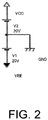
- Fig. 2 illustrates power supply voltages VCC and VEE.
- an operational amplifier IC1, a resistor R1, and a resistor R2 are amplifying circuits 10 for an input signal e1 which is input from an input terminal t1.
- An oscillator 12 that outputs the input signal e1 which is a pulse having a predetermined frequency is connected to the input terminal t1.
- the input signal is a music signal obtained during a musical performance of an electric guitar connected to a guitar amplifier.
- the amplifying circuit 10 illustrated in Fig. 1 is a non-inversion amplifying circuit, but an inversion amplifying circuit may be applied.
- a speaker load 30 is connected to an output terminal t2 of the amplifier.
- the speaker load 30 includes a resistor R5 which is a pure resistance component of a speaker unit and a parasitic induction component L2.
- a speaker unit adopted for a general guitar amplifier is assumed.
- a jumping-up circuit 20 (first jumping-up circuit) is inserted between the amplifying circuit 10 and the output terminal t2. That is, a signal from the amplifying circuit 10 passes through the jumping-up circuit 20 and is then connected to the speaker load 30.
- the jumping-up circuit 20 is a resonance circuit including a coil L1 which is a inductive load and capacitors C1 and C2 which are capacitive loads, in the example illustrated in Fig. 1 .
- a jumping-up circuit 20A (second jumping-up circuit) which is a resonance circuit having damping resistors R6 and R7 added thereto may be adopted.
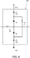
- a configuration of a jumping-up circuit 20B (third jumping-up circuit) having diodes D1 and D2 which are rectifying elements and a resistor R3 added thereto may be adopted.
- Fig. 5 illustrates an output waveform (a lower part of Fig. 4 ) output to a speaker load observed in a case where a rectangular wave (an upper part of Fig. 4 ) having a period of 1 kHz is input to a vacuum tube amplifier. According to the vacuum tube amplifier, a so-called jumping-up waveform output having the following characteristics is observed.
- an input signal (e1) for the amplifier illustrated in Fig. 1 a rectangular wave having a period of 1 kHz based on a positive-side waveform and a negative-side waveform is adopted. This is a waveform suitable for observing characteristics of a so-called attack waveform immediately after picking a guitar, among assumed output musical sound waveforms of the electric guitar.
- Fig. 6 illustrates input and output waveforms of the jumping-up circuits 20, 20A, and 20B.
- An uppermost part in Fig. 6 shows a waveform at an observation point (2) in Fig. 1 , that is, an input waveform for the jumping-up circuit.
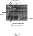
- a second part from the top in Fig. 6 and Fig. 7 shows a waveform at an observation point (3) in Fig. 1 , that is, an output waveform of the jumping-up circuit 20 in a case where the jumping-up circuit 20 is adopted.
- an output waveform of the jumping-up circuit 20 With respect to an input waveform, an output waveform of the jumping-up circuit 20 generates a resonance wave (ringing) having a plurality of peaks during rising and falling of the waveform.
- a peak value of a first peak including resonance exceeds a power supply voltage ( ⁇ 40 V), and a so-called jumping-up effect is generated. This is because resonance occurs due to L1 and (C1+C2) during rising and falling of a waveform.
- An output waveform shown in a third part from the top in Fig. 6 shows an output waveform of the jumping-up circuit 20A (a waveform at an observation point (3) in Fig. 1 ) with respect to an input waveform shown in an uppermost part.
- an output waveform of the jumping-up circuit 20 (a second part from the top in Fig. 6 )
- resonance of the coil L1 and the capacitor C1 and resonance of the coil L1 and the capacitor C2 are suppressed by the application of a damping effect obtained by the resistors R6 and R7.
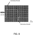
- An output waveform shown in a fourth part (a lowermost part) from the top in Fig. 6 and Fig. 8 shows an output waveform of the jumping-up circuit 20B (the waveform at the observation point (3) in Fig. 1 ) with respect to the input waveform in the uppermost part.
- a resonance wave (overshooting and undershooting) having a first peak is generated during rising and falling corresponding to rising and falling of an input pulse.
- a peak value of the first peak including resonance exceeds a power supply voltage ( ⁇ 40 V), which leads to a so-called jumping-up effect.
- Fig. 9 illustrates an equivalent circuit of the jumping-up circuit 20B in a case where a positive-side input waveform is input to the jumping-up circuit 20B.
- the equivalent circuit includes a capacitor C1 which is a first capacitive load, a capacitor C2 which is a second capacitive load including a resistor R3 which is a damping element, and a diode D1 which is a rectifying element connected between the capacitor C1 and a coil L1 which is an inductive load.
- overshooting of a first peak illustrated in Fig. 8 occurs due to resonance between the coil L1 and the capacitors C1 and C2.
- resonance between the capacitor C1 and the coil L1 which does not pass through the damping resistor R3 has a dominant effect.
- the capacitor C2 is charged with a delay charge through the damping resistor R3.
- the resonance between the coil L1 and the capacitor C1 induces undershooting of the first peak and the second and subsequent peaks.
- the capacitor C2 is charged with a delay charge, and thus the occurrence of undershooting of the first peak and peaks after the second peak and the subsequent induced due to the resonance of the coil L1 and the capacitor C1 is suppressed by an integration circuit constituted by the resistor R3 and the capacitor C2.
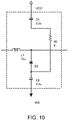
- Fig. 10 illustrates an equivalent circuit of the jumping-up circuit 20B in a case where a negative-side input waveform is input to the jumping-up circuit 20B.
- functional roles of the capacitor C1 and the capacitor C2 are switched when comparing with the configuration of Fig. 9 , but the capacitors are operated according to the same principle as in the above description when a positive-side waveform is input.
- an electronic inductive load or an electronic capacitive load constituted by an electronic circuit and the like may be applied instead of the coil L and the capacitor C.
- the jumping-up circuits 20, 20A, and 20B of the amplifier 1 according to the embodiment it is possible to obtain an output waveform causing overshooting and undershooting which exceed a power supply voltage in response to rising and falling of an input pulse using the jumping-up circuit.
- the jumping-up circuits 20A or 20B it is possible to obtain an output waveform approximating to an output waveform of a vacuum tube amplifier by suppressing ringing.
- the configurations described in the embodiment can be appropriately combined within a range that does not deviate from the objective.
Landscapes
- Engineering & Computer Science (AREA)
- Physics & Mathematics (AREA)
- Multimedia (AREA)
- Power Engineering (AREA)
- Nonlinear Science (AREA)
- Acoustics & Sound (AREA)
- Signal Processing (AREA)
- Amplifiers (AREA)
- Circuit For Audible Band Transducer (AREA)
- Control Of Amplification And Gain Control (AREA)
Abstract

Description
- The present disclosure relates to an amplifier for a music signal and a method of outputting a waveform of a music signal.
- Conventionally, it has become known that a circuit simulating the electrical characteristics of a vacuum tube can be applied to a guitar amplifier, and a technique for simulating the input and output characteristics characteristic to a vacuum tube amplifier is known (see, for example, Patent Document 1). In addition, an invention simulating the distortion impression characteristic to a vacuum tube amplifier by adjusting a filter multiplier according to the level of a guitar input signal has been proposed (see, for example, Patent Document 2).
-
- [Patent Document 1] Japanese Examined Patent Application, Second Publication No.
S59-051167 - [Patent Document 2] Japanese Patent No.
3336089 - In the related art, even when the shape of a waveform of a vacuum tube amplifier can be simulated, a waveform exceeding a power supply voltage cannot be output.
- The disclosure provides an amplifier capable of outputting a waveform of a music signal exceeding a power supply voltage.
- According to an embodiment, there is provided an amplifier comprising a power supply, an input terminal for a music signal, an amplifying circuit which amplifies the music signal using the power supply, and a circuit which is connected to an output end of the amplifying circuit and outputs a waveform exceeding a voltage value of the power supply. The circuit is, for example, a jumping-up circuit.
- For the amplifier, a configuration in which an output end of the jumping-up circuit is connected to a speaker load in series may be adopted. In addition, for the circuit in the amplifier, a configuration including a jumping-up control circuit that controls an output waveform of the circuit may be adopted.
- In addition, a configuration in which the jumping-up circuit in the amplifier is a resonance circuit including an inductive load and a capacitive load may be adopted. In addition, a configuration in which the jumping-up circuit is a resonance circuit including an inductive load, a first capacitive load, and a rectifying element connected between the inductive load and the capacitive load may be adopted. In addition, a configuration in which the jumping-up circuit is a resonance circuit including an inductive load, a first capacitive load, a second capacitive load including a damping element, and a rectifying element connected between the inductive load and the first capacitive load may be adopted.
-
-
Fig. 1 illustrates a circuit configuration of an amplifier (power amplifier) which is applicable to a guitar amplifier. -
Fig. 2 illustrates power supply voltages of the amplifier. -
Fig. 3 illustrates a configuration example of a jumping-up circuit. -
Fig. 4 illustrates a configuration example of a jumping-up circuit. -
Fig. 5 illustrates an example of an input and output waveform of a vacuum tube amplifier. -
Fig. 6 illustrates an input waveform for a jumping-up circuit and output waveforms of first to third jumping-up circuits. -
Fig. 7 illustrates the output waveform of the first jumping-up circuit. -
Fig. 8 illustrates the output waveform of the third jumping-up circuit. -
Fig. 9 illustrates an equivalent circuit in a case where a positive-side input signal is input to the third jumping-up circuit. -
Fig. 10 illustrates an equivalent circuit in a case where a negative-side input signal is input to the third jumping-up circuit. - Hereinafter, an embodiment of an amplifying circuit will be described with reference to the drawings. A configuration of the embodiment is an example, and the disclosure is not limited thereto.
Fig. 1 illustrates a circuit configuration of an amplifier 1 (amplifying circuit: power amplifier) which is applicable to a guitar amplifier. Theamplifier 1 is configured such that a waveform obtained by simulating a vacuum tube amplifier is obtained.Fig. 2 illustrates power supply voltages VCC and VEE. - In
Fig. 1 , an operational amplifier IC1, a resistor R1, and a resistor R2 are amplifyingcircuits 10 for an input signal e1 which is input from an input terminal t1. Anoscillator 12 that outputs the input signal e1 which is a pulse having a predetermined frequency is connected to the input terminal t1. The input signal is a music signal obtained during a musical performance of an electric guitar connected to a guitar amplifier. Meanwhile, the amplifyingcircuit 10 illustrated inFig. 1 is a non-inversion amplifying circuit, but an inversion amplifying circuit may be applied. - A
speaker load 30 is connected to an output terminal t2 of the amplifier. Thespeaker load 30 includes a resistor R5 which is a pure resistance component of a speaker unit and a parasitic induction component L2. For the speaker unit, a speaker unit adopted for a general guitar amplifier is assumed. - A jumping-up circuit 20 (first jumping-up circuit) is inserted between the amplifying
circuit 10 and the output terminal t2. That is, a signal from the amplifyingcircuit 10 passes through the jumping-upcircuit 20 and is then connected to thespeaker load 30. The jumping-upcircuit 20 is a resonance circuit including a coil L1 which is a inductive load and capacitors C1 and C2 which are capacitive loads, in the example illustrated inFig. 1 . However, as illustrated inFig. 3 , a jumping-upcircuit 20A (second jumping-up circuit) which is a resonance circuit having damping resistors R6 and R7 added thereto may be adopted. Alternatively, as illustrated inFig. 4 , a configuration of a jumping-up circuit 20B (third jumping-up circuit) having diodes D1 and D2 which are rectifying elements and a resistor R3 added thereto may be adopted. -
Fig. 5 illustrates an output waveform (a lower part ofFig. 4 ) output to a speaker load observed in a case where a rectangular wave (an upper part ofFig. 4 ) having a period of 1 kHz is input to a vacuum tube amplifier. According to the vacuum tube amplifier, a so-called jumping-up waveform output having the following characteristics is observed. - (1) A waveform jumps up particularly greatly (an overshoot occurs) during rising and falling of the waveform.
- (2) A peak voltage value (peak value) of jumping-up is a value larger than a power supply voltage.
- As an input signal (e1) for the amplifier illustrated in
Fig. 1 , a rectangular wave having a period of 1 kHz based on a positive-side waveform and a negative-side waveform is adopted. This is a waveform suitable for observing characteristics of a so-called attack waveform immediately after picking a guitar, among assumed output musical sound waveforms of the electric guitar. -
Fig. 6 illustrates input and output waveforms of the jumping-upcircuits Fig. 6 shows a waveform at an observation point (2) inFig. 1 , that is, an input waveform for the jumping-up circuit. A second part from the top inFig. 6 andFig. 7 shows a waveform at an observation point (3) inFig. 1 , that is, an output waveform of the jumping-upcircuit 20 in a case where the jumping-upcircuit 20 is adopted. - With respect to an input waveform, an output waveform of the jumping-up
circuit 20 generates a resonance wave (ringing) having a plurality of peaks during rising and falling of the waveform. A peak value of a first peak including resonance exceeds a power supply voltage (± 40 V), and a so-called jumping-up effect is generated. This is because resonance occurs due to L1 and (C1+C2) during rising and falling of a waveform. - However, as illustrated in
Fig. 7 , undershooting of the first peak and a peak after the subsequent second peak occurs subsequently to overshooting of the first peak, which results in an attenuation state while oscillating. In this manner, a waveform which jumps up (jumps down) particularly greatly during rising and falling of a waveform which is a feature of a waveform of a vacuum tube amplifier, as illustrated inFig. 5 , is not obtained. - An output waveform shown in a third part from the top in
Fig. 6 shows an output waveform of the jumping-upcircuit 20A (a waveform at an observation point (3) inFig. 1 ) with respect to an input waveform shown in an uppermost part. As compared with an output waveform of the jumping-up circuit 20 (a second part from the top inFig. 6 ), resonance of the coil L1 and the capacitor C1 and resonance of the coil L1 and the capacitor C2 are suppressed by the application of a damping effect obtained by the resistors R6 and R7. - However, in the output waveform of the jumping-up
circuit 20A, peaks after the second peak is occurred (ringing occurred) following the overshooting of the first peak and the undershooting of the first peak, and thus a waveform in which one overshooting or undershooting occurs as in an output waveform of a vacuum tube amplifier (Fig. 5 ) is not obtained. - An output waveform shown in a fourth part (a lowermost part) from the top in
Fig. 6 andFig. 8 shows an output waveform of the jumping-upcircuit 20B (the waveform at the observation point (3) inFig. 1 ) with respect to the input waveform in the uppermost part. In the output waveform of the jumping-upcircuit 20B, a resonance wave (overshooting and undershooting) having a first peak is generated during rising and falling corresponding to rising and falling of an input pulse. A peak value of the first peak including resonance exceeds a power supply voltage (± 40 V), which leads to a so-called jumping-up effect. - In addition, as compared with the jumping-up
circuit circuit 20B, and thus it can be said that ringing does not occur. That is, a waveform close to an output waveform of a vacuum tube amplifier is obtained. -
Fig. 9 illustrates an equivalent circuit of the jumping-upcircuit 20B in a case where a positive-side input waveform is input to the jumping-upcircuit 20B. The equivalent circuit includes a capacitor C1 which is a first capacitive load, a capacitor C2 which is a second capacitive load including a resistor R3 which is a damping element, and a diode D1 which is a rectifying element connected between the capacitor C1 and a coil L1 which is an inductive load. When an operation of the jumping-upcircuit 20B is described using the equivalent circuit, overshooting of a first peak illustrated inFig. 8 occurs due to resonance between the coil L1 and the capacitors C1 and C2. In this case, resonance between the capacitor C1 and the coil L1 which does not pass through the damping resistor R3 has a dominant effect. In the meantime, the capacitor C2 is charged with a delay charge through the damping resistor R3. - After the overshooting of the first peak, the resonance between the coil L1 and the capacitor C1 induces undershooting of the first peak and the second and subsequent peaks. However, the capacitor C2 is charged with a delay charge, and thus the occurrence of undershooting of the first peak and peaks after the second peak and the subsequent induced due to the resonance of the coil L1 and the capacitor C1 is suppressed by an integration circuit constituted by the resistor R3 and the capacitor C2.
-
Fig. 10 illustrates an equivalent circuit of the jumping-upcircuit 20B in a case where a negative-side input waveform is input to the jumping-upcircuit 20B. In a configuration ofFig. 10 , functional roles of the capacitor C1 and the capacitor C2 are switched when comparing with the configuration ofFig. 9 , but the capacitors are operated according to the same principle as in the above description when a positive-side waveform is input. - Meanwhile, an electronic inductive load or an electronic capacitive load constituted by an electronic circuit and the like may be applied instead of the coil L and the capacitor C. As described above, according to the jumping-up
circuits amplifier 1 according to the embodiment, it is possible to obtain an output waveform causing overshooting and undershooting which exceed a power supply voltage in response to rising and falling of an input pulse using the jumping-up circuit. In addition, according to the jumping-upcircuits -
- 1 Amplifier
- 10 Amplifying circuit
- 20, 20A, 20B Jumping-up circuit
- 30 Speaker load
Claims (15)
- An amplifier (1) comprising:a power supply;an input terminal (t1) for a music signal;an amplifying circuit (10) which amplifies the music signal using the power supply; anda circuit (20, 20A, 20B) which is connected to an output end of the amplifying circuit (10) and outputs a waveform exceeding a voltage value of the power supply.
- The amplifier (1) according to claim 1, wherein
the circuit (20, 20A, 20B) is a jumping-up circuit (20, 20A, 20B). - The amplifier (1) according to claim 1 or 2, wherein
an output end of the circuit (20, 20A, 20B) is connected to a speaker load (30) in series. - The amplifier (1) according to any one of claims 1 to 3, wherein
the circuit (20, 20A, 20B) includes a jumping-up control circuit controlling an output waveform of the circuit (20, 20A, 20B). - The amplifier (1) according to any one of claims 1 to 4, wherein
the circuit (20, 20A, 20B) is a resonance circuit including an inductive load and a capacitive load. - The amplifier (1) according to any one of claims 1 to 4, wherein
the circuit (20, 20A, 20B) is a resonance circuit including an inductive load, a capacitive load, and a rectifying element connected between the inductive load and the capacitive load. - The amplifier (1) according to any one of claims 1 to 4, wherein
the circuit (20, 20A, 20B) is a resonance circuit including an inductive load, a first capacitive load, a second capacitive load including a damping element, and a rectifying element connected between the inductive load and the first capacitive load. - The amplifier (1) according to any one of claims 1 to 7, wherein
an output waveform of the circuit (20, 20A, 20B) generates a resonance wave having a plurality of peaks during rising and falling of a waveform with respect to an input waveform of the music signal, and a jumping-up effect is generated. - The amplifier (1) according to claim 8, wherein
the resonance wave is generated due to an inductive load and a capacitive load of the circuit (20, 20A, 20B). - A method of outputting a waveform of a music signal, the method comprising:amplifying the music signal by an amplifying circuit (10) using a power supply; andoutputting a waveform exceeding a voltage value of the power supply by a circuit (20, 20A, 20B) connected to an output end of the amplifying circuit (10).
- The method of outputting a waveform of a music signal according to claim 10, wherein
the circuit (20, 20A, 20B) is a jumping-up circuit (20, 20A, 20B). - The method of outputting a waveform of a music signal according to claim 10 or 11, wherein
an output end of the circuit (20, 20A, 20B) is connected to a speaker load (30) in series. - The method of outputting a waveform of a music signal according to any one of claims 10 to 12, wherein
an output waveform of the circuit (20, 20A, 20B) generates a resonance wave having a plurality of peaks during rising and falling of a waveform with respect to an input waveform of the music signal, and a jumping-up effect is generated. - The method of outputting a waveform of a music signal according to claim 13, wherein
the resonance wave is generated due to an inductive load and a capacitive load of the circuit (20, 20A, 20B). - The method of outputting a waveform of a music signal according to any one of claims 10 to 14, further comprising:
charging a capacitive load with a delay charge through a damping element.
Applications Claiming Priority (1)
| Application Number | Priority Date | Filing Date | Title |
|---|---|---|---|
| JP2019239930A JP7411411B2 (en) | 2019-12-27 | 2019-12-27 | Musical signal amplifier |
Publications (2)
| Publication Number | Publication Date |
|---|---|
| EP3843266A1 true EP3843266A1 (en) | 2021-06-30 |
| EP3843266B1 EP3843266B1 (en) | 2022-06-08 |
Family
ID=73838906
Family Applications (1)
| Application Number | Title | Priority Date | Filing Date |
|---|---|---|---|
| EP20213993.7A Active EP3843266B1 (en) | 2019-12-27 | 2020-12-15 | Amplifier for music signal and method of outputting waveform of music signal |
Country Status (4)
| Country | Link |
|---|---|
| US (1) | US11670272B2 (en) |
| EP (1) | EP3843266B1 (en) |
| JP (1) | JP7411411B2 (en) |
| CN (1) | CN113131907B (en) |
Families Citing this family (1)
| Publication number | Priority date | Publication date | Assignee | Title |
|---|---|---|---|---|
| JP7411411B2 (en) * | 2019-12-27 | 2024-01-11 | ローランド株式会社 | Musical signal amplifier |
Citations (4)
| Publication number | Priority date | Publication date | Assignee | Title |
|---|---|---|---|---|
| US3648188A (en) * | 1970-06-10 | 1972-03-07 | Bendix Corp | Transistor power amplifier |
| JPS5951167B2 (en) | 1976-05-13 | 1984-12-12 | ソニー株式会社 | gain control circuit |
| JP3336089B2 (en) | 1993-09-16 | 2002-10-21 | ローランド株式会社 | Signal processing device |
| US20180233950A1 (en) * | 2017-02-13 | 2018-08-16 | STMicroelectronics (Grand Ouest) SAS | Method and device for the contactless energy transfer to an apparatus equipped with a loudspeaker |
Family Cites Families (28)
| Publication number | Priority date | Publication date | Assignee | Title |
|---|---|---|---|---|
| JPS5951167A (en) | 1982-09-16 | 1984-03-24 | Tokyo Keiki Co Ltd | Hydraulic operating motor |
| US4936185A (en) * | 1986-12-25 | 1990-06-26 | Yamaha Corporation | Electronic musical instrument having plural component blocks |
| US4809336A (en) * | 1987-03-23 | 1989-02-28 | Pritchard Eric K | Semiconductor amplifier with tube amplifier characteristics |
| JPH1155041A (en) * | 1997-08-06 | 1999-02-26 | Roland Corp | Power amplifier |
| CN1293864A (en) * | 1999-02-04 | 2001-05-02 | 松下电器产业株式会社 | power circuit |
| DE19953119C2 (en) | 1999-11-04 | 2003-03-20 | Harman Audio Electronic Sys | Audio amplifier with a clocked power amplifier |
| JP3941549B2 (en) | 2002-03-06 | 2007-07-04 | ヤマハ株式会社 | Class D amplifier |
| JP3928515B2 (en) * | 2002-07-31 | 2007-06-13 | ヤマハ株式会社 | Class D amplifier |
| JP3922129B2 (en) * | 2002-08-02 | 2007-05-30 | ヤマハ株式会社 | Class D amplifier |
| JP2004128599A (en) * | 2002-09-30 | 2004-04-22 | Ricoh Co Ltd | Operational amplifier and speaker amplifier using the operational amplifier |
| JP2006135778A (en) * | 2004-11-08 | 2006-05-25 | Mitsubishi Electric Engineering Co Ltd | Parametric speaker |
| JP4802765B2 (en) * | 2005-03-18 | 2011-10-26 | ヤマハ株式会社 | Class D amplifier |
| JP2007189621A (en) * | 2006-01-16 | 2007-07-26 | Kenwood Corp | Amplifier and amplifying method |
| WO2008062748A1 (en) * | 2006-11-20 | 2008-05-29 | Panasonic Corporation | Signal processing device and signal processing method |
| US8428271B1 (en) * | 2009-03-20 | 2013-04-23 | Charles Michael Luke | Balanced distortion for musical instrument |
| JP5710870B2 (en) * | 2009-09-28 | 2015-04-30 | ローランド株式会社 | DC-DC converter |
| US8390373B2 (en) * | 2010-06-08 | 2013-03-05 | MUSIC Group IP Ltd. | Ultra-high efficiency switching power inverter and power amplifier |
| US9203365B1 (en) * | 2011-07-18 | 2015-12-01 | Michael B. Milbert | Lightweight amplifier |
| KR101784799B1 (en) | 2011-08-01 | 2017-10-12 | 삼성전자주식회사 | Swiching amp sound output device, audio apparatus and method for sound output thereof |
| US9008333B2 (en) | 2011-11-29 | 2015-04-14 | Quilter Labs, LLC | Guitar amplifier |
| JP2016111430A (en) * | 2014-12-03 | 2016-06-20 | ローム株式会社 | Pwm modulation device and audio signal output device |
| JP6651835B2 (en) | 2015-03-13 | 2020-02-19 | ヤマハ株式会社 | Power amplifier |
| US9680432B2 (en) * | 2015-03-13 | 2017-06-13 | Yamaha Corporation | Power amplifier and input signal adjusting method |
| US10158327B2 (en) * | 2016-10-28 | 2018-12-18 | Qualcomm Incorporated | Low impedance adaptive bias scheme for power amplifier |
| US10869127B2 (en) * | 2017-01-02 | 2020-12-15 | Frank Joseph Pompei | Amplifier interface and amplification methods for ultrasound devices |
| JP7101590B2 (en) * | 2018-10-18 | 2022-07-15 | エイブリック株式会社 | Switching regulator |
| US11164551B2 (en) * | 2019-02-28 | 2021-11-02 | Clifford W. Chase | Amplifier matching in a digital amplifier modeling system |
| JP7411411B2 (en) * | 2019-12-27 | 2024-01-11 | ローランド株式会社 | Musical signal amplifier |
-
2019
- 2019-12-27 JP JP2019239930A patent/JP7411411B2/en active Active
-
2020
- 2020-12-15 EP EP20213993.7A patent/EP3843266B1/en active Active
- 2020-12-17 CN CN202011493592.7A patent/CN113131907B/en active Active
- 2020-12-22 US US17/129,936 patent/US11670272B2/en active Active
Patent Citations (4)
| Publication number | Priority date | Publication date | Assignee | Title |
|---|---|---|---|---|
| US3648188A (en) * | 1970-06-10 | 1972-03-07 | Bendix Corp | Transistor power amplifier |
| JPS5951167B2 (en) | 1976-05-13 | 1984-12-12 | ソニー株式会社 | gain control circuit |
| JP3336089B2 (en) | 1993-09-16 | 2002-10-21 | ローランド株式会社 | Signal processing device |
| US20180233950A1 (en) * | 2017-02-13 | 2018-08-16 | STMicroelectronics (Grand Ouest) SAS | Method and device for the contactless energy transfer to an apparatus equipped with a loudspeaker |
Also Published As
| Publication number | Publication date |
|---|---|
| JP2021108438A (en) | 2021-07-29 |
| EP3843266B1 (en) | 2022-06-08 |
| CN113131907A (en) | 2021-07-16 |
| US11670272B2 (en) | 2023-06-06 |
| CN113131907B (en) | 2026-04-07 |
| US20210201879A1 (en) | 2021-07-01 |
| JP7411411B2 (en) | 2024-01-11 |
Similar Documents
| Publication | Publication Date | Title |
|---|---|---|
| TWI452810B (en) | Mixed mode compensation circuit and method for a power converter | |
| US8115537B2 (en) | Method and apparatus for suppressing noise caused by parasitic capacitance and/or resistance in an electronic circuit or system | |
| KR101120492B1 (en) | Class-d amplifier | |
| CN102545662A (en) | Switch control circuit, converter using the same, and switch control method | |
| JP4155211B2 (en) | Switching power supply | |
| JPS62248399A (en) | Hearing aide | |
| CN111585525B (en) | Class D transconductance amplifier | |
| CN106160709B (en) | Systems and methods for reducing switching losses in a power conversion system | |
| TW200840174A (en) | Method of forming a power supply controller and structure therefor | |
| US9960675B2 (en) | Feed-forward control system with current estimator | |
| CN108572276B (en) | Wireless resonant power transmitter and method of peak-to-peak voltage detection therein | |
| CN112260530B (en) | Power soft start control circuit, control chip and control device | |
| KR100977505B1 (en) | drive | |
| EP2725368A2 (en) | Impedance source ranging apparatus and method | |
| US11670272B2 (en) | Amplifier for music signal and method of outputting waveform of music signal | |
| CN107846152A (en) | For with the method and system of duty cycle adjustment crest frequency | |
| CN108700901B (en) | Vibration Control Device | |
| KR20160111010A (en) | Switching element driving circuit | |
| CN102217180B (en) | Control circuit for a primary-controlled switched-mode power supply with increased voltage regulation accuracy, as well as a primary-controlled switched-mode power supply | |
| KR100588704B1 (en) | Power circuit and test device | |
| TW201340564A (en) | A sampling circuit for power converter | |
| US6344982B1 (en) | Power supply circuit | |
| JP2016035220A (en) | Semiconductor device | |
| JP3477619B1 (en) | Electronic load device | |
| JP2002335682A (en) | Steep wave voltage generator |
Legal Events
| Date | Code | Title | Description |
|---|---|---|---|
| PUAI | Public reference made under article 153(3) epc to a published international application that has entered the european phase |
Free format text: ORIGINAL CODE: 0009012 |
|
| STAA | Information on the status of an ep patent application or granted ep patent |
Free format text: STATUS: THE APPLICATION HAS BEEN PUBLISHED |
|
| AK | Designated contracting states |
Kind code of ref document: A1 Designated state(s): AL AT BE BG CH CY CZ DE DK EE ES FI FR GB GR HR HU IE IS IT LI LT LU LV MC MK MT NL NO PL PT RO RS SE SI SK SM TR |
|
| STAA | Information on the status of an ep patent application or granted ep patent |
Free format text: STATUS: REQUEST FOR EXAMINATION WAS MADE |
|
| 17P | Request for examination filed |
Effective date: 20211208 |
|
| RBV | Designated contracting states (corrected) |
Designated state(s): AL AT BE BG CH CY CZ DE DK EE ES FI FR GB GR HR HU IE IS IT LI LT LU LV MC MK MT NL NO PL PT RO RS SE SI SK SM TR |
|
| GRAP | Despatch of communication of intention to grant a patent |
Free format text: ORIGINAL CODE: EPIDOSNIGR1 |
|
| STAA | Information on the status of an ep patent application or granted ep patent |
Free format text: STATUS: GRANT OF PATENT IS INTENDED |
|
| INTG | Intention to grant announced |
Effective date: 20220203 |
|
| GRAS | Grant fee paid |
Free format text: ORIGINAL CODE: EPIDOSNIGR3 |
|
| GRAA | (expected) grant |
Free format text: ORIGINAL CODE: 0009210 |
|
| STAA | Information on the status of an ep patent application or granted ep patent |
Free format text: STATUS: THE PATENT HAS BEEN GRANTED |
|
| AK | Designated contracting states |
Kind code of ref document: B1 Designated state(s): AL AT BE BG CH CY CZ DE DK EE ES FI FR GB GR HR HU IE IS IT LI LT LU LV MC MK MT NL NO PL PT RO RS SE SI SK SM TR |
|
| REG | Reference to a national code |
Ref country code: AT Ref legal event code: REF Ref document number: 1497619 Country of ref document: AT Kind code of ref document: T Effective date: 20220615 Ref country code: CH Ref legal event code: EP |
|
| REG | Reference to a national code |
Ref country code: DE Ref legal event code: R096 Ref document number: 602020003481 Country of ref document: DE |
|
| REG | Reference to a national code |
Ref country code: IE Ref legal event code: FG4D |
|
| REG | Reference to a national code |
Ref country code: LT Ref legal event code: MG9D |
|
| REG | Reference to a national code |
Ref country code: NL Ref legal event code: MP Effective date: 20220608 |
|
| PG25 | Lapsed in a contracting state [announced via postgrant information from national office to epo] |
Ref country code: SE Free format text: LAPSE BECAUSE OF FAILURE TO SUBMIT A TRANSLATION OF THE DESCRIPTION OR TO PAY THE FEE WITHIN THE PRESCRIBED TIME-LIMIT Effective date: 20220608 Ref country code: NO Free format text: LAPSE BECAUSE OF FAILURE TO SUBMIT A TRANSLATION OF THE DESCRIPTION OR TO PAY THE FEE WITHIN THE PRESCRIBED TIME-LIMIT Effective date: 20220908 Ref country code: LT Free format text: LAPSE BECAUSE OF FAILURE TO SUBMIT A TRANSLATION OF THE DESCRIPTION OR TO PAY THE FEE WITHIN THE PRESCRIBED TIME-LIMIT Effective date: 20220608 Ref country code: HR Free format text: LAPSE BECAUSE OF FAILURE TO SUBMIT A TRANSLATION OF THE DESCRIPTION OR TO PAY THE FEE WITHIN THE PRESCRIBED TIME-LIMIT Effective date: 20220608 Ref country code: GR Free format text: LAPSE BECAUSE OF FAILURE TO SUBMIT A TRANSLATION OF THE DESCRIPTION OR TO PAY THE FEE WITHIN THE PRESCRIBED TIME-LIMIT Effective date: 20220909 Ref country code: FI Free format text: LAPSE BECAUSE OF FAILURE TO SUBMIT A TRANSLATION OF THE DESCRIPTION OR TO PAY THE FEE WITHIN THE PRESCRIBED TIME-LIMIT Effective date: 20220608 Ref country code: BG Free format text: LAPSE BECAUSE OF FAILURE TO SUBMIT A TRANSLATION OF THE DESCRIPTION OR TO PAY THE FEE WITHIN THE PRESCRIBED TIME-LIMIT Effective date: 20220908 |
|
| REG | Reference to a national code |
Ref country code: AT Ref legal event code: MK05 Ref document number: 1497619 Country of ref document: AT Kind code of ref document: T Effective date: 20220608 |
|
| PG25 | Lapsed in a contracting state [announced via postgrant information from national office to epo] |
Ref country code: RS Free format text: LAPSE BECAUSE OF FAILURE TO SUBMIT A TRANSLATION OF THE DESCRIPTION OR TO PAY THE FEE WITHIN THE PRESCRIBED TIME-LIMIT Effective date: 20220608 Ref country code: LV Free format text: LAPSE BECAUSE OF FAILURE TO SUBMIT A TRANSLATION OF THE DESCRIPTION OR TO PAY THE FEE WITHIN THE PRESCRIBED TIME-LIMIT Effective date: 20220608 |
|
| PG25 | Lapsed in a contracting state [announced via postgrant information from national office to epo] |
Ref country code: NL Free format text: LAPSE BECAUSE OF FAILURE TO SUBMIT A TRANSLATION OF THE DESCRIPTION OR TO PAY THE FEE WITHIN THE PRESCRIBED TIME-LIMIT Effective date: 20220608 |
|
| PG25 | Lapsed in a contracting state [announced via postgrant information from national office to epo] |
Ref country code: SM Free format text: LAPSE BECAUSE OF FAILURE TO SUBMIT A TRANSLATION OF THE DESCRIPTION OR TO PAY THE FEE WITHIN THE PRESCRIBED TIME-LIMIT Effective date: 20220608 Ref country code: SK Free format text: LAPSE BECAUSE OF FAILURE TO SUBMIT A TRANSLATION OF THE DESCRIPTION OR TO PAY THE FEE WITHIN THE PRESCRIBED TIME-LIMIT Effective date: 20220608 Ref country code: RO Free format text: LAPSE BECAUSE OF FAILURE TO SUBMIT A TRANSLATION OF THE DESCRIPTION OR TO PAY THE FEE WITHIN THE PRESCRIBED TIME-LIMIT Effective date: 20220608 Ref country code: PT Free format text: LAPSE BECAUSE OF FAILURE TO SUBMIT A TRANSLATION OF THE DESCRIPTION OR TO PAY THE FEE WITHIN THE PRESCRIBED TIME-LIMIT Effective date: 20221010 Ref country code: ES Free format text: LAPSE BECAUSE OF FAILURE TO SUBMIT A TRANSLATION OF THE DESCRIPTION OR TO PAY THE FEE WITHIN THE PRESCRIBED TIME-LIMIT Effective date: 20220608 Ref country code: EE Free format text: LAPSE BECAUSE OF FAILURE TO SUBMIT A TRANSLATION OF THE DESCRIPTION OR TO PAY THE FEE WITHIN THE PRESCRIBED TIME-LIMIT Effective date: 20220608 Ref country code: CZ Free format text: LAPSE BECAUSE OF FAILURE TO SUBMIT A TRANSLATION OF THE DESCRIPTION OR TO PAY THE FEE WITHIN THE PRESCRIBED TIME-LIMIT Effective date: 20220608 Ref country code: AT Free format text: LAPSE BECAUSE OF FAILURE TO SUBMIT A TRANSLATION OF THE DESCRIPTION OR TO PAY THE FEE WITHIN THE PRESCRIBED TIME-LIMIT Effective date: 20220608 |
|
| PG25 | Lapsed in a contracting state [announced via postgrant information from national office to epo] |
Ref country code: PL Free format text: LAPSE BECAUSE OF FAILURE TO SUBMIT A TRANSLATION OF THE DESCRIPTION OR TO PAY THE FEE WITHIN THE PRESCRIBED TIME-LIMIT Effective date: 20220608 Ref country code: IS Free format text: LAPSE BECAUSE OF FAILURE TO SUBMIT A TRANSLATION OF THE DESCRIPTION OR TO PAY THE FEE WITHIN THE PRESCRIBED TIME-LIMIT Effective date: 20221008 |
|
| REG | Reference to a national code |
Ref country code: DE Ref legal event code: R097 Ref document number: 602020003481 Country of ref document: DE |
|
| PG25 | Lapsed in a contracting state [announced via postgrant information from national office to epo] |
Ref country code: AL Free format text: LAPSE BECAUSE OF FAILURE TO SUBMIT A TRANSLATION OF THE DESCRIPTION OR TO PAY THE FEE WITHIN THE PRESCRIBED TIME-LIMIT Effective date: 20220608 |
|
| PLBE | No opposition filed within time limit |
Free format text: ORIGINAL CODE: 0009261 |
|
| STAA | Information on the status of an ep patent application or granted ep patent |
Free format text: STATUS: NO OPPOSITION FILED WITHIN TIME LIMIT |
|
| PG25 | Lapsed in a contracting state [announced via postgrant information from national office to epo] |
Ref country code: DK Free format text: LAPSE BECAUSE OF FAILURE TO SUBMIT A TRANSLATION OF THE DESCRIPTION OR TO PAY THE FEE WITHIN THE PRESCRIBED TIME-LIMIT Effective date: 20220608 |
|
| 26N | No opposition filed |
Effective date: 20230310 |
|
| PG25 | Lapsed in a contracting state [announced via postgrant information from national office to epo] |
Ref country code: SI Free format text: LAPSE BECAUSE OF FAILURE TO SUBMIT A TRANSLATION OF THE DESCRIPTION OR TO PAY THE FEE WITHIN THE PRESCRIBED TIME-LIMIT Effective date: 20220608 |
|
| P01 | Opt-out of the competence of the unified patent court (upc) registered |
Effective date: 20230517 |
|
| REG | Reference to a national code |
Ref country code: BE Ref legal event code: MM Effective date: 20221231 |
|
| PG25 | Lapsed in a contracting state [announced via postgrant information from national office to epo] |
Ref country code: LU Free format text: LAPSE BECAUSE OF NON-PAYMENT OF DUE FEES Effective date: 20221215 |
|
| PG25 | Lapsed in a contracting state [announced via postgrant information from national office to epo] |
Ref country code: IE Free format text: LAPSE BECAUSE OF NON-PAYMENT OF DUE FEES Effective date: 20221215 |
|
| PG25 | Lapsed in a contracting state [announced via postgrant information from national office to epo] |
Ref country code: BE Free format text: LAPSE BECAUSE OF NON-PAYMENT OF DUE FEES Effective date: 20221231 |
|
| PG25 | Lapsed in a contracting state [announced via postgrant information from national office to epo] |
Ref country code: IT Free format text: LAPSE BECAUSE OF FAILURE TO SUBMIT A TRANSLATION OF THE DESCRIPTION OR TO PAY THE FEE WITHIN THE PRESCRIBED TIME-LIMIT Effective date: 20220608 |
|
| PG25 | Lapsed in a contracting state [announced via postgrant information from national office to epo] |
Ref country code: CY Free format text: LAPSE BECAUSE OF FAILURE TO SUBMIT A TRANSLATION OF THE DESCRIPTION OR TO PAY THE FEE WITHIN THE PRESCRIBED TIME-LIMIT Effective date: 20220608 |
|
| PG25 | Lapsed in a contracting state [announced via postgrant information from national office to epo] |
Ref country code: MK Free format text: LAPSE BECAUSE OF FAILURE TO SUBMIT A TRANSLATION OF THE DESCRIPTION OR TO PAY THE FEE WITHIN THE PRESCRIBED TIME-LIMIT Effective date: 20220608 |
|
| PG25 | Lapsed in a contracting state [announced via postgrant information from national office to epo] |
Ref country code: MC Free format text: LAPSE BECAUSE OF FAILURE TO SUBMIT A TRANSLATION OF THE DESCRIPTION OR TO PAY THE FEE WITHIN THE PRESCRIBED TIME-LIMIT Effective date: 20220608 |
|
| PG25 | Lapsed in a contracting state [announced via postgrant information from national office to epo] |
Ref country code: TR Free format text: LAPSE BECAUSE OF FAILURE TO SUBMIT A TRANSLATION OF THE DESCRIPTION OR TO PAY THE FEE WITHIN THE PRESCRIBED TIME-LIMIT Effective date: 20220608 Ref country code: MC Free format text: LAPSE BECAUSE OF FAILURE TO SUBMIT A TRANSLATION OF THE DESCRIPTION OR TO PAY THE FEE WITHIN THE PRESCRIBED TIME-LIMIT Effective date: 20220608 |
|
| REG | Reference to a national code |
Ref country code: CH Ref legal event code: PL |
|
| PG25 | Lapsed in a contracting state [announced via postgrant information from national office to epo] |
Ref country code: MT Free format text: LAPSE BECAUSE OF FAILURE TO SUBMIT A TRANSLATION OF THE DESCRIPTION OR TO PAY THE FEE WITHIN THE PRESCRIBED TIME-LIMIT Effective date: 20220608 |
|
| PG25 | Lapsed in a contracting state [announced via postgrant information from national office to epo] |
Ref country code: CH Free format text: LAPSE BECAUSE OF NON-PAYMENT OF DUE FEES Effective date: 20231231 |
|
| PG25 | Lapsed in a contracting state [announced via postgrant information from national office to epo] |
Ref country code: CH Free format text: LAPSE BECAUSE OF NON-PAYMENT OF DUE FEES Effective date: 20231231 |
|
| PG25 | Lapsed in a contracting state [announced via postgrant information from national office to epo] |
Ref country code: BG Free format text: LAPSE BECAUSE OF FAILURE TO SUBMIT A TRANSLATION OF THE DESCRIPTION OR TO PAY THE FEE WITHIN THE PRESCRIBED TIME-LIMIT Effective date: 20220608 |
|
| PG25 | Lapsed in a contracting state [announced via postgrant information from national office to epo] |
Ref country code: BG Free format text: LAPSE BECAUSE OF FAILURE TO SUBMIT A TRANSLATION OF THE DESCRIPTION OR TO PAY THE FEE WITHIN THE PRESCRIBED TIME-LIMIT Effective date: 20220608 |
|
| PG25 | Lapsed in a contracting state [announced via postgrant information from national office to epo] |
Ref country code: HU Free format text: LAPSE BECAUSE OF FAILURE TO SUBMIT A TRANSLATION OF THE DESCRIPTION OR TO PAY THE FEE WITHIN THE PRESCRIBED TIME-LIMIT; INVALID AB INITIO Effective date: 20201215 |
|
| PGFP | Annual fee paid to national office [announced via postgrant information from national office to epo] |
Ref country code: DE Payment date: 20251028 Year of fee payment: 6 |
|
| PGFP | Annual fee paid to national office [announced via postgrant information from national office to epo] |
Ref country code: GB Payment date: 20251030 Year of fee payment: 6 |
|
| PGFP | Annual fee paid to national office [announced via postgrant information from national office to epo] |
Ref country code: FR Payment date: 20251110 Year of fee payment: 6 |
|
| PG25 | Lapsed in a contracting state [announced via postgrant information from national office to epo] |
Ref country code: CH Free format text: THE PATENT HAS BEEN ANNULLED BY A DECISION OF A NATIONAL AUTHORITY Effective date: 20231231 |