EP3840039A1 - A semiconductor device and corresponding method - Google Patents
A semiconductor device and corresponding method Download PDFInfo
- Publication number
- EP3840039A1 EP3840039A1 EP20213302.1A EP20213302A EP3840039A1 EP 3840039 A1 EP3840039 A1 EP 3840039A1 EP 20213302 A EP20213302 A EP 20213302A EP 3840039 A1 EP3840039 A1 EP 3840039A1
- Authority
- EP
- European Patent Office
- Prior art keywords
- electrically conductive
- enlarged end
- molding material
- end portions
- semiconductor device
- Prior art date
- Legal status (The legal status is an assumption and is not a legal conclusion. Google has not performed a legal analysis and makes no representation as to the accuracy of the status listed.)
- Granted
Links
Images

Classifications
-
- H—ELECTRICITY
- H10—SEMICONDUCTOR DEVICES; ELECTRIC SOLID-STATE DEVICES NOT OTHERWISE PROVIDED FOR
- H10W—GENERIC PACKAGES, INTERCONNECTIONS, CONNECTORS OR OTHER CONSTRUCTIONAL DETAILS OF DEVICES COVERED BY CLASS H10
- H10W70/00—Package substrates; Interposers; Redistribution layers [RDL]
- H10W70/60—Insulating or insulated package substrates; Interposers; Redistribution layers
- H10W70/62—Insulating or insulated package substrates; Interposers; Redistribution layers characterised by their interconnections
- H10W70/65—Shapes or dispositions of interconnections
- H10W70/657—Shapes or dispositions of interconnections on sidewalls or bottom surfaces of the package substrates, interposers or redistribution layers
-
- H—ELECTRICITY
- H10—SEMICONDUCTOR DEVICES; ELECTRIC SOLID-STATE DEVICES NOT OTHERWISE PROVIDED FOR
- H10W—GENERIC PACKAGES, INTERCONNECTIONS, CONNECTORS OR OTHER CONSTRUCTIONAL DETAILS OF DEVICES COVERED BY CLASS H10
- H10W70/00—Package substrates; Interposers; Redistribution layers [RDL]
- H10W70/40—Leadframes
- H10W70/421—Shapes or dispositions
- H10W70/424—Cross-sectional shapes
-
- H—ELECTRICITY
- H10—SEMICONDUCTOR DEVICES; ELECTRIC SOLID-STATE DEVICES NOT OTHERWISE PROVIDED FOR
- H10W—GENERIC PACKAGES, INTERCONNECTIONS, CONNECTORS OR OTHER CONSTRUCTIONAL DETAILS OF DEVICES COVERED BY CLASS H10
- H10W70/00—Package substrates; Interposers; Redistribution layers [RDL]
- H10W70/40—Leadframes
- H10W70/464—Additional interconnections in combination with leadframes
- H10W70/465—Bumps or wires
-
- H—ELECTRICITY
- H10—SEMICONDUCTOR DEVICES; ELECTRIC SOLID-STATE DEVICES NOT OTHERWISE PROVIDED FOR
- H10W—GENERIC PACKAGES, INTERCONNECTIONS, CONNECTORS OR OTHER CONSTRUCTIONAL DETAILS OF DEVICES COVERED BY CLASS H10
- H10W70/00—Package substrates; Interposers; Redistribution layers [RDL]
- H10W70/01—Manufacture or treatment
- H10W70/04—Manufacture or treatment of leadframes
- H10W70/047—Attaching leadframes to insulating supports, e.g. for tape automated bonding [TAB]
-
- H—ELECTRICITY
- H10—SEMICONDUCTOR DEVICES; ELECTRIC SOLID-STATE DEVICES NOT OTHERWISE PROVIDED FOR
- H10W—GENERIC PACKAGES, INTERCONNECTIONS, CONNECTORS OR OTHER CONSTRUCTIONAL DETAILS OF DEVICES COVERED BY CLASS H10
- H10W70/00—Package substrates; Interposers; Redistribution layers [RDL]
- H10W70/40—Leadframes
- H10W70/421—Shapes or dispositions
-
- H—ELECTRICITY
- H10—SEMICONDUCTOR DEVICES; ELECTRIC SOLID-STATE DEVICES NOT OTHERWISE PROVIDED FOR
- H10W—GENERIC PACKAGES, INTERCONNECTIONS, CONNECTORS OR OTHER CONSTRUCTIONAL DETAILS OF DEVICES COVERED BY CLASS H10
- H10W70/00—Package substrates; Interposers; Redistribution layers [RDL]
- H10W70/40—Leadframes
- H10W70/456—Materials
- H10W70/457—Materials of metallic layers on leadframes
-
- H—ELECTRICITY
- H10—SEMICONDUCTOR DEVICES; ELECTRIC SOLID-STATE DEVICES NOT OTHERWISE PROVIDED FOR
- H10W—GENERIC PACKAGES, INTERCONNECTIONS, CONNECTORS OR OTHER CONSTRUCTIONAL DETAILS OF DEVICES COVERED BY CLASS H10
- H10W70/00—Package substrates; Interposers; Redistribution layers [RDL]
- H10W70/60—Insulating or insulated package substrates; Interposers; Redistribution layers
- H10W70/62—Insulating or insulated package substrates; Interposers; Redistribution layers characterised by their interconnections
- H10W70/66—Conductive materials thereof
-
- H—ELECTRICITY
- H10—SEMICONDUCTOR DEVICES; ELECTRIC SOLID-STATE DEVICES NOT OTHERWISE PROVIDED FOR
- H10W—GENERIC PACKAGES, INTERCONNECTIONS, CONNECTORS OR OTHER CONSTRUCTIONAL DETAILS OF DEVICES COVERED BY CLASS H10
- H10W74/00—Encapsulations, e.g. protective coatings
- H10W74/01—Manufacture or treatment
- H10W74/016—Manufacture or treatment using moulds
-
- H—ELECTRICITY
- H10—SEMICONDUCTOR DEVICES; ELECTRIC SOLID-STATE DEVICES NOT OTHERWISE PROVIDED FOR
- H10W—GENERIC PACKAGES, INTERCONNECTIONS, CONNECTORS OR OTHER CONSTRUCTIONAL DETAILS OF DEVICES COVERED BY CLASS H10
- H10W74/00—Encapsulations, e.g. protective coatings
- H10W74/10—Encapsulations, e.g. protective coatings characterised by their shape or disposition
- H10W74/111—Encapsulations, e.g. protective coatings characterised by their shape or disposition the semiconductor body being completely enclosed
-
- H—ELECTRICITY
- H10—SEMICONDUCTOR DEVICES; ELECTRIC SOLID-STATE DEVICES NOT OTHERWISE PROVIDED FOR
- H10W—GENERIC PACKAGES, INTERCONNECTIONS, CONNECTORS OR OTHER CONSTRUCTIONAL DETAILS OF DEVICES COVERED BY CLASS H10
- H10W72/00—Interconnections or connectors in packages
- H10W72/01—Manufacture or treatment
- H10W72/0198—Manufacture or treatment batch processes
-
- H—ELECTRICITY
- H10—SEMICONDUCTOR DEVICES; ELECTRIC SOLID-STATE DEVICES NOT OTHERWISE PROVIDED FOR
- H10W—GENERIC PACKAGES, INTERCONNECTIONS, CONNECTORS OR OTHER CONSTRUCTIONAL DETAILS OF DEVICES COVERED BY CLASS H10
- H10W72/00—Interconnections or connectors in packages
- H10W72/071—Connecting or disconnecting
- H10W72/072—Connecting or disconnecting of bump connectors
-
- H—ELECTRICITY
- H10—SEMICONDUCTOR DEVICES; ELECTRIC SOLID-STATE DEVICES NOT OTHERWISE PROVIDED FOR
- H10W—GENERIC PACKAGES, INTERCONNECTIONS, CONNECTORS OR OTHER CONSTRUCTIONAL DETAILS OF DEVICES COVERED BY CLASS H10
- H10W72/00—Interconnections or connectors in packages
- H10W72/071—Connecting or disconnecting
- H10W72/072—Connecting or disconnecting of bump connectors
- H10W72/07251—Connecting or disconnecting of bump connectors characterised by changes in properties of the bump connectors during connecting
- H10W72/07253—Connecting or disconnecting of bump connectors characterised by changes in properties of the bump connectors during connecting changes in shapes
-
- H—ELECTRICITY
- H10—SEMICONDUCTOR DEVICES; ELECTRIC SOLID-STATE DEVICES NOT OTHERWISE PROVIDED FOR
- H10W—GENERIC PACKAGES, INTERCONNECTIONS, CONNECTORS OR OTHER CONSTRUCTIONAL DETAILS OF DEVICES COVERED BY CLASS H10
- H10W72/00—Interconnections or connectors in packages
- H10W72/071—Connecting or disconnecting
- H10W72/075—Connecting or disconnecting of bond wires
-
- H—ELECTRICITY
- H10—SEMICONDUCTOR DEVICES; ELECTRIC SOLID-STATE DEVICES NOT OTHERWISE PROVIDED FOR
- H10W—GENERIC PACKAGES, INTERCONNECTIONS, CONNECTORS OR OTHER CONSTRUCTIONAL DETAILS OF DEVICES COVERED BY CLASS H10
- H10W72/00—Interconnections or connectors in packages
- H10W72/30—Die-attach connectors
- H10W72/351—Materials of die-attach connectors
- H10W72/352—Materials of die-attach connectors comprising metals or metalloids, e.g. solders
-
- H—ELECTRICITY
- H10—SEMICONDUCTOR DEVICES; ELECTRIC SOLID-STATE DEVICES NOT OTHERWISE PROVIDED FOR
- H10W—GENERIC PACKAGES, INTERCONNECTIONS, CONNECTORS OR OTHER CONSTRUCTIONAL DETAILS OF DEVICES COVERED BY CLASS H10
- H10W72/00—Interconnections or connectors in packages
- H10W72/30—Die-attach connectors
- H10W72/351—Materials of die-attach connectors
- H10W72/353—Materials of die-attach connectors not comprising solid metals or solid metalloids, e.g. ceramics
- H10W72/354—Materials of die-attach connectors not comprising solid metals or solid metalloids, e.g. ceramics comprising polymers
-
- H—ELECTRICITY
- H10—SEMICONDUCTOR DEVICES; ELECTRIC SOLID-STATE DEVICES NOT OTHERWISE PROVIDED FOR
- H10W—GENERIC PACKAGES, INTERCONNECTIONS, CONNECTORS OR OTHER CONSTRUCTIONAL DETAILS OF DEVICES COVERED BY CLASS H10
- H10W72/00—Interconnections or connectors in packages
- H10W72/851—Dispositions of multiple connectors or interconnections
- H10W72/874—On different surfaces
- H10W72/884—Die-attach connectors and bond wires
-
- H—ELECTRICITY
- H10—SEMICONDUCTOR DEVICES; ELECTRIC SOLID-STATE DEVICES NOT OTHERWISE PROVIDED FOR
- H10W—GENERIC PACKAGES, INTERCONNECTIONS, CONNECTORS OR OTHER CONSTRUCTIONAL DETAILS OF DEVICES COVERED BY CLASS H10
- H10W90/00—Package configurations
- H10W90/701—Package configurations characterised by the relative positions of pads or connectors relative to package parts
- H10W90/731—Package configurations characterised by the relative positions of pads or connectors relative to package parts of die-attach connectors
- H10W90/736—Package configurations characterised by the relative positions of pads or connectors relative to package parts of die-attach connectors between a chip and a stacked lead frame, conducting package substrate or heat sink
-
- H—ELECTRICITY
- H10—SEMICONDUCTOR DEVICES; ELECTRIC SOLID-STATE DEVICES NOT OTHERWISE PROVIDED FOR
- H10W—GENERIC PACKAGES, INTERCONNECTIONS, CONNECTORS OR OTHER CONSTRUCTIONAL DETAILS OF DEVICES COVERED BY CLASS H10
- H10W90/00—Package configurations
- H10W90/701—Package configurations characterised by the relative positions of pads or connectors relative to package parts
- H10W90/751—Package configurations characterised by the relative positions of pads or connectors relative to package parts of bond wires
- H10W90/756—Package configurations characterised by the relative positions of pads or connectors relative to package parts of bond wires between a chip and a stacked lead frame, conducting package substrate or heat sink
Definitions
- the description relates to manufacturing semiconductor devices.
- One or more embodiments may be applied to manufacturing integrated circuits (ICs).
- ICs integrated circuits
- Quad-flat no-leads (QFN) packages and land grid array (LGA) packages are examples of surface-mount technology (SMT) packages known in the art.
- SMT surface-mount technology
- QFN packages are near chip-scale plastic encapsulated packages provided with a planar leadframe substrate, wherein perimeter lands on the package rear (e.g., bottom) side are configured to provide electrical connections to a printed circuit board (PCB).
- the leads of the leadframe are thus fully incorporated in the package molding compound.
- QFN packages may include an exposed thermal pad to improve heat transfer out of the integrated circuit, into the printed circuit board.
- LGA packages also have leads fully incorporated in the package molding compound, and comprise a (rectangular) grid of contacts on the bottom side of the package.
- the contacts on the package are configured to be coupled to a grid of contacts on the PCB.
- Both QFN and LGA packages do not have external leads, but rather have "lands” or “pads” that are directly couplable to the PCB pads for soldering by means of solder paste or solder alloy.
- the mounting (soldering) step may be complex and may result in a wide variability of welding strength and structure. Additionally, the different coefficients of thermal expansion between the package and the printed circuit board may lead to high stress in the solder material and/or to high thermal fatigue of QFN/LGA packages once mounted on a printed circuit board.
- Wettable flanks help increasing leads wettability with the purpose of improving solder adhesion and overall welding strength by increasing the solder attach area on the vertical side of the lands or pads. Wettable flanks may only slightly improve the solder joint reliability, and facilitate automatic optical inspection of the solder joint after the surface mounting process, for surface mount process control.
- Packaged semiconductor devices providing improved solder joint reliability and/or stronger anchorage to the PCB are desirable.
- An object of one or more embodiments is to contribute in providing packaged semiconductor devices, e.g., comprising a QFN- or LGA-type package, with improved solder joint reliability and/or stronger anchorage to the printed circuit board.
- such an object can be achieved by means of a semiconductor device (e.g., an integrated circuit) having the features set forth in the claims that follow.
- a semiconductor device e.g., an integrated circuit
- One or more embodiments may relate to a corresponding method of manufacturing semiconductor devices.
- One or more embodiments may provide a packaged semiconductor device (e.g., comprising a QFN or LGA package) comprising at least one semiconductor die electrically coupled to a set of electrically conductive leads, and package molding material molded over the at least one semiconductor die and the electrically conductive leads. At least a portion of the electrically conductive leads may be exposed at a rear surface of the package molding material to provide electrically conductive pads.
- the electrically conductive pads may comprise enlarged end portions extending at least partially over the package molding material and configured for coupling to a printed circuit board.
- references to "an embodiment” or “one embodiment” in the framework of the present description is intended to indicate that a particular configuration, structure, or characteristic described in relation to the embodiment is comprised in at least one embodiment.
- phrases such as “in an embodiment” or “in one embodiment” that may be present in one or more points of the present description do not necessarily refer to one and the same embodiment.
- particular conformations, structures, or characteristics may be combined in any adequate way in one or more embodiments.
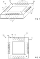
- Figures 1 and 2 are exemplary of a semiconductor device 10 comprising a QFN package.
- a semiconductor device 10 as exemplified herein may comprise package molding material 100 encapsulating a semiconductor die (not visible in Figures 1 and 2 ), the molding material 100 being shaped to provide a rear (e.g., bottom) side 10A of the semiconductor device 10 configured for electrical and mechanical coupling to a printed circuit board.
- a set of electrically conductive "lands" or “pads” 12 may be provided on the rear (or bottom) side 10A, e.g., at the periphery thereof, as illustrated in Figures 1 and 2 . Additionally or alternatively, the pads 12 may be arranged over the entire area of the rear side 10A, as customary in LGA packages. The pads 12 may be electrically coupled to the semiconductor die encapsulated in the molding material 100.
- the package may include an exposed thermal pad 14 on the rear side 10A.
- the thermal pad 14 may be thermally coupled to the semiconductor die encapsulated in the molding material 100 to improve heat transfer out of the integrated circuit 10.
- the electrical pads 12 and the thermal pad 14 may provide the leadframe of the integrated circuit 10.
- FIG. 1 shows a bottom view of an exemplary integrated circuit 10 having electrical pads 12 and a thermal pad 14 (illustrated with solid lines), and a corresponding exemplary arrangement of solder pads 12' and 14' as may be present on a printed circuit board configured for coupling to the integrated circuit 10.
- Figure 3A is a magnified view exemplary of a portion of the rear side 10A of the integrated circuit 10, e.g., portion 20 illustrated in Figure 2 .
- Figure 3B is a corresponding side view of portion 20, exemplary of the integrated circuit 10 mounted on a printed circuit board 30 by means of soldering material 32 interposed between the electrical pads 12 of the integrated circuit 10 and the respective solder pads 12' on the PCB 30.
- reliability of such electro-mechanical coupling may be improved by increasing the area of the electrical pads 12 of the integrated circuit 10.
- Figure 4A is a magnified view exemplary of a portion 20 of the rear side 10A of an integrated circuit 10 according to one or more embodiments.
- Figure 4B is a corresponding side view of portion 20, exemplary of the integrated circuit 10 mounted on a printed circuit board 30 by means of soldering material 42.
- a metallic layer may be selectively provided at the pads 12 after molding of the package material 100 to provide enlarged end portions 44 of the pads.
- the enlarged end portions 44 may thus partially extend over the molding material 100 at the interface between the pads 12 and the molding material 100 (e.g., "sidewise" of the body portion 12 of the pads which are embedded in the molding material), thereby increasing the area of the pads suitable for electrical and/or mechanical coupling to the soldering pads 12'.
- a (thick) "pedestal" of metal material may be grown over the surface of the pads 12 and/or 14 left exposed by the molding material 100, thereby providing larger pads (i.e., providing a reduced spacing D n between pads 12, which increase the soldering surface) and an increase of the standoff between the semiconductor package 100 and the printed circuit board 30.
- solder joint reliability may be improved and/or a stronger anchorage of the integrated circuit to the PCB may be obtained.
- the enlarged end portions 44 may be provided (e.g., grown) over the pads 12 and/or 14 after molding of the package material 100 by means of galvanic plating.
- Providing the enlarged end portions 44 by galvanic plating may be advantageous insofar as it may facilitate growing the metal 44 (sidewise) over the molding compound 100 at the interface between the pads 12 and/or 14 and the molding compound 100, i.e., it may facilitate properly increasing the area of the pads (as exemplified in Figure 4B ).
- any other selective metal deposition technique that would result in an isotropic growth of metal at the pads 12 and/or 14 may be used to form the enlarged portions 44.
- the thickness of the enlarged end portions 44 may be in the range of 10 ⁇ m to 100 ⁇ m, preferably 50 ⁇ m to 70 ⁇ m.
- the enlarged end portions 44 may extend (sidewise) over the molding compound 100 from the interface between the respective body portion of pad 12 and/or 14 and the molding compound 100 (see length D p in Figure 4B ) for about 10 ⁇ m to 100 ⁇ m, preferably 50 ⁇ m to 70 ⁇ m.
- the enlarged end portions 44 may comprise at least one metal selected out of copper (Cu), nickel (Ni), palladium (Pd) and gold (Au).
- the enlarged end portions 44 comprise copper (Cu).
- a further metallic layer may be provided over the enlarged end portions 44.
- the further metallic layer may comprise tin (Sn) plated over the enlarged end portions 44 at the pads 12 and/or 14.
- One or more embodiments may provide improved reliability (e.g., longer life on board) over previous solutions, e.g., over solutions involving wettable flanks.
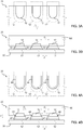
- Figures 5A to 5G are exemplary of possible steps of a method of manufacturing semiconductor devices according to one or more embodiments. In such Figures, manufacturing of a pair of semiconductor devices in exemplified.
- an otherwise conventional leadframe may be provided as a first manufacturing step.
- the leadframe may comprise a die pad 14 and respective leads 12.
- At least one semiconductor die 50 may be mounted on each die pad 14 of the leadframe.
- the semiconductor dies 50 may be attached on the die pads 14 via die attach material 52, e.g., soft-solder die attach material and/or glue.
- wire bonding may be carried out to provide electrical coupling between a semiconductor die 50 and the respective leads 12 via bonding wires 54.
- package molding material 100 may be molded to encapsulate the semiconductor dies 50 and the leadframe, leaving exposed the electrical pads 12 and the thermal pads 14 at the rear side of the semiconductor devices.
- a metallic layer 44 may be provided at the pads 12 and/or 14 after molding of the package material 100, thereby providing metallic "bumps" (the enlarged end portions) at the package leads.
- the enlarged end portions 44 may be grown, for instance, by galvanic plating.
- the thickness ( t ) of the enlarged end portions 44 may be in the range of 10 ⁇ m to 100 ⁇ m, preferably 50 ⁇ m to 70 ⁇ m.
- the lateral extension ( D p ) of the enlarged end portions 44 may be in the range of 10 ⁇ m to 100 ⁇ m, preferably 50 ⁇ m to 70 ⁇ m.
- the enlarged end portions 44 may comprise one or more metals selected out of copper (Cu), nickel (Ni), palladium (Pd) and gold (Au) .
- a further metallic layer 56 may be provided over the metallic layer 44, e.g., by plating.
- the further metallic layer 56 may comprise tin (Sn).
- the manufacturing method may comprise singulating the semiconductor devices 10, e.g., by cutting or sawing along sawing lines, as conventional in the art.
- a semiconductor device (e.g., 10) may comprise:
- the electrically conductive pads may comprise enlarged end portions (e.g., 44) extending at least partially over the package molding material, the enlarged end portions configured for coupling to a printed circuit board (e.g., 30).
- the electrically conductive pads may comprise body portions (e.g., stem portions or web portions 12) embedded in the package molding material and the enlarged end portions may protrude from the package molding material.
- the enlarged end portions may extend over the package molding material sidewise of said body portions for a length (e.g., D p ) of 10 ⁇ m to 100 ⁇ m, preferably 50 ⁇ m to 70 ⁇ m.
- the enlarged end portions may comprise galvanic plating grown material.
- the enlarged end portions may comprise at least one metal selected out of copper, nickel, palladium and gold, preferably copper.
- a thickness (e.g., t ) of the enlarged end portions may be in the range of 10 ⁇ m to 100 ⁇ m, preferably 50 ⁇ m to 70 ⁇ m.
- a semiconductor device may comprise a metallic layer (e.g., 56) plated over the enlarged end portions.
- the metallic layer may comprise tin.
- a semiconductor device may comprise a thermally conductive pad (e.g., 14).
- the thermally conductive pad may comprise a respective enlarged end portion extending at least partially over the package molding material and configured for coupling to a printed circuit board.
- a semiconductor device may comprise a quad-flat no-lead package or a land grid array package.
- a method may comprise:
Landscapes
- Structures Or Materials For Encapsulating Or Coating Semiconductor Devices Or Solid State Devices (AREA)
- Lead Frames For Integrated Circuits (AREA)
Abstract
Description
- The description relates to manufacturing semiconductor devices.
- One or more embodiments may be applied to manufacturing integrated circuits (ICs).
- Semiconductor devices such as integrated circuits may be provided with packages of various types. For instance, quad-flat no-leads (QFN) packages and land grid array (LGA) packages are examples of surface-mount technology (SMT) packages known in the art.
- QFN packages are near chip-scale plastic encapsulated packages provided with a planar leadframe substrate, wherein perimeter lands on the package rear (e.g., bottom) side are configured to provide electrical connections to a printed circuit board (PCB). The leads of the leadframe are thus fully incorporated in the package molding compound. QFN packages may include an exposed thermal pad to improve heat transfer out of the integrated circuit, into the printed circuit board.
- LGA packages also have leads fully incorporated in the package molding compound, and comprise a (rectangular) grid of contacts on the bottom side of the package. The contacts on the package are configured to be coupled to a grid of contacts on the PCB.
- Both QFN and LGA packages (as well as other SMT packages) do not have external leads, but rather have "lands" or "pads" that are directly couplable to the PCB pads for soldering by means of solder paste or solder alloy. The mounting (soldering) step may be complex and may result in a wide variability of welding strength and structure. Additionally, the different coefficients of thermal expansion between the package and the printed circuit board may lead to high stress in the solder material and/or to high thermal fatigue of QFN/LGA packages once mounted on a printed circuit board.
- In this context, the use of "wettable flanks" is known in the art. Wettable flanks help increasing leads wettability with the purpose of improving solder adhesion and overall welding strength by increasing the solder attach area on the vertical side of the lands or pads. Wettable flanks may only slightly improve the solder joint reliability, and facilitate automatic optical inspection of the solder joint after the surface mounting process, for surface mount process control.
- Packaged semiconductor devices providing improved solder joint reliability and/or stronger anchorage to the PCB are desirable.
- An object of one or more embodiments is to contribute in providing packaged semiconductor devices, e.g., comprising a QFN- or LGA-type package, with improved solder joint reliability and/or stronger anchorage to the printed circuit board.
- According to one or more embodiments, such an object can be achieved by means of a semiconductor device (e.g., an integrated circuit) having the features set forth in the claims that follow.
- One or more embodiments may relate to a corresponding method of manufacturing semiconductor devices.
- The claims are an integral part of the technical teaching provided herein in respect of the embodiments.
- One or more embodiments may provide a packaged semiconductor device (e.g., comprising a QFN or LGA package) comprising at least one semiconductor die electrically coupled to a set of electrically conductive leads, and package molding material molded over the at least one semiconductor die and the electrically conductive leads. At least a portion of the electrically conductive leads may be exposed at a rear surface of the package molding material to provide electrically conductive pads. The electrically conductive pads may comprise enlarged end portions extending at least partially over the package molding material and configured for coupling to a printed circuit board.
- One or more embodiments will now be described, by way of example only, with reference to the annexed figures, wherein:
-
Figure 1 is a perspective view exemplary of a semiconductor device comprising a QFN package, shown upside-down (i.e., with the rear side facing upwards), -
Figure 2 is a view of the rear side of the semiconductor device ofFigure 1 , -
Figure 3A is a magnified view of a portion of the rear side of the semiconductor device ofFigure 2 , -
Figure 3B is a side view of the portion of the semiconductor device ofFigure 3A mounted on a printed circuit board, -
Figure 4A is a magnified view of a portion of the rear side of a semiconductor device according to embodiments, -
Figure 4B is a side view of the portion of the semiconductor device ofFigure 4A mounted on a printed circuit board, and -
Figures 5A to 5G are exemplary of steps of a method of manufacturing semiconductor devices according to embodiments. - In the ensuing description, one or more specific details are illustrated, aimed at providing an in-depth understanding of examples of embodiments of this description. The embodiments may be obtained without one or more of the specific details, or with other methods, components, materials, etc. In other cases, known structures, materials, or operations are not illustrated or described in detail so that certain aspects of embodiments will not be obscured.
- Reference to "an embodiment" or "one embodiment" in the framework of the present description is intended to indicate that a particular configuration, structure, or characteristic described in relation to the embodiment is comprised in at least one embodiment. Hence, phrases such as "in an embodiment" or "in one embodiment" that may be present in one or more points of the present description do not necessarily refer to one and the same embodiment. Moreover, particular conformations, structures, or characteristics may be combined in any adequate way in one or more embodiments.
- Throughout the figures annexed herein, like parts or elements are indicated with like references/numerals and a corresponding description will not be repeated for brevity.
- The references used herein are provided merely for convenience and hence do not define the extent of protection or the scope of the embodiments.
- By way of introduction to the detailed description of exemplary embodiments, reference may be first had to
Figures 1 and 2 , which are exemplary of asemiconductor device 10 comprising a QFN package. - While reference is made mainly to QFN packages in the present description and drawings for the sake of conciseness, one or more embodiments may be applied to other types of "leadless" packages, e.g., LGA packages.
- As current in the art, together with other elements/features not visible in the Figures, a
semiconductor device 10 as exemplified herein may comprisepackage molding material 100 encapsulating a semiconductor die (not visible inFigures 1 and 2 ), themolding material 100 being shaped to provide a rear (e.g., bottom)side 10A of thesemiconductor device 10 configured for electrical and mechanical coupling to a printed circuit board. - A set of electrically conductive "lands" or "pads" 12 may be provided on the rear (or bottom)
side 10A, e.g., at the periphery thereof, as illustrated inFigures 1 and 2 . Additionally or alternatively, thepads 12 may be arranged over the entire area of therear side 10A, as customary in LGA packages. Thepads 12 may be electrically coupled to the semiconductor die encapsulated in themolding material 100. - Optionally, the package may include an exposed
thermal pad 14 on therear side 10A. Thethermal pad 14 may be thermally coupled to the semiconductor die encapsulated in themolding material 100 to improve heat transfer out of the integratedcircuit 10. - Overall, the
electrical pads 12 and thethermal pad 14 may provide the leadframe of the integratedcircuit 10. - The (minimum) spacing between two
subsequent pads 12 may be constrained by manufacturing constraints of the leadframe. Typically, the corresponding solder pads on a PCB may be wider and/or less spaced. For instance,Figure 2 shows a bottom view of an exemplaryintegrated circuit 10 havingelectrical pads 12 and a thermal pad 14 (illustrated with solid lines), and a corresponding exemplary arrangement of solder pads 12' and 14' as may be present on a printed circuit board configured for coupling to the integratedcircuit 10. -
Figure 3A is a magnified view exemplary of a portion of therear side 10A of the integratedcircuit 10, e.g.,portion 20 illustrated inFigure 2 .Figure 3B is a corresponding side view ofportion 20, exemplary of the integratedcircuit 10 mounted on a printedcircuit board 30 by means of solderingmaterial 32 interposed between theelectrical pads 12 of the integratedcircuit 10 and the respective solder pads 12' on thePCB 30. - It is noted that, as a consequence of the spacing Do between
pads 12 being (considerably) larger than the spacing d between pads 12', electro-mechanical coupling of the integratedcircuit 10 to thePCB 30 may turn out to be unsatisfactory. - In one or more embodiments as exemplified in
Figures 4A and 4B , reliability of such electro-mechanical coupling may be improved by increasing the area of theelectrical pads 12 of the integratedcircuit 10. -
Figure 4A is a magnified view exemplary of aportion 20 of therear side 10A of an integratedcircuit 10 according to one or more embodiments.Figure 4B is a corresponding side view ofportion 20, exemplary of the integratedcircuit 10 mounted on a printedcircuit board 30 by means ofsoldering material 42. - As exemplified herein, a metallic layer may be selectively provided at the
pads 12 after molding of thepackage material 100 to provide enlargedend portions 44 of the pads. The enlargedend portions 44 may thus partially extend over themolding material 100 at the interface between thepads 12 and the molding material 100 (e.g., "sidewise" of thebody portion 12 of the pads which are embedded in the molding material), thereby increasing the area of the pads suitable for electrical and/or mechanical coupling to the soldering pads 12'. - Therefore, in one or more embodiments, a (thick) "pedestal" of metal material may be grown over the surface of the
pads 12 and/or 14 left exposed by themolding material 100, thereby providing larger pads (i.e., providing a reduced spacing Dn betweenpads 12, which increase the soldering surface) and an increase of the standoff between thesemiconductor package 100 and the printedcircuit board 30. As a result, solder joint reliability may be improved and/or a stronger anchorage of the integrated circuit to the PCB may be obtained. - In one or more embodiments, the
enlarged end portions 44 may be provided (e.g., grown) over thepads 12 and/or 14 after molding of thepackage material 100 by means of galvanic plating. - Providing the
enlarged end portions 44 by galvanic plating may be advantageous insofar as it may facilitate growing the metal 44 (sidewise) over themolding compound 100 at the interface between thepads 12 and/or 14 and themolding compound 100, i.e., it may facilitate properly increasing the area of the pads (as exemplified inFigure 4B ). - Additionally or alternatively, any other selective metal deposition technique that would result in an isotropic growth of metal at the
pads 12 and/or 14 may be used to form theenlarged portions 44. - In one or more embodiments, the thickness of the
enlarged end portions 44 may be in the range of 10 µm to 100 µm, preferably 50 µm to 70 µm. - In one or more embodiments, the
enlarged end portions 44 may extend (sidewise) over themolding compound 100 from the interface between the respective body portion ofpad 12 and/or 14 and the molding compound 100 (see length Dp inFigure 4B ) for about 10 µm to 100 µm, preferably 50 µm to 70 µm. - In one or more embodiments, the
enlarged end portions 44 may comprise at least one metal selected out of copper (Cu), nickel (Ni), palladium (Pd) and gold (Au). Preferably, theenlarged end portions 44 comprise copper (Cu). - In one or more embodiments, a further metallic layer may be provided over the
enlarged end portions 44. For instance, the further metallic layer may comprise tin (Sn) plated over theenlarged end portions 44 at thepads 12 and/or 14. - One or more embodiments may provide improved reliability (e.g., longer life on board) over previous solutions, e.g., over solutions involving wettable flanks.
-
Figures 5A to 5G are exemplary of possible steps of a method of manufacturing semiconductor devices according to one or more embodiments. In such Figures, manufacturing of a pair of semiconductor devices in exemplified. - As exemplified in
Figure 5A , an otherwise conventional leadframe may be provided as a first manufacturing step. For each semiconductor device, the leadframe may comprise adie pad 14 and respective leads 12. - As exemplified in
Figure 5B , at least one semiconductor die 50 may be mounted on eachdie pad 14 of the leadframe. For instance, the semiconductor dies 50 may be attached on thedie pads 14 via die attachmaterial 52, e.g., soft-solder die attach material and/or glue. - As exemplified in
Figure 5C , wire bonding may be carried out to provide electrical coupling between asemiconductor die 50 and the respective leads 12 viabonding wires 54. - As exemplified in
Figure 5D ,package molding material 100 may be molded to encapsulate the semiconductor dies 50 and the leadframe, leaving exposed theelectrical pads 12 and thethermal pads 14 at the rear side of the semiconductor devices. - As exemplified in
Figure 5E , ametallic layer 44 may be provided at thepads 12 and/or 14 after molding of thepackage material 100, thereby providing metallic "bumps" (the enlarged end portions) at the package leads. Theenlarged end portions 44 may be grown, for instance, by galvanic plating. The thickness (t) of theenlarged end portions 44 may be in the range of 10 µm to 100 µm, preferably 50 µm to 70 µm. The lateral extension (Dp ) of theenlarged end portions 44 may be in the range of 10 µm to 100 µm, preferably 50 µm to 70 µm. Theenlarged end portions 44 may comprise one or more metals selected out of copper (Cu), nickel (Ni), palladium (Pd) and gold (Au) . - As exemplified in
Figure 5F , a furthermetallic layer 56 may be provided over themetallic layer 44, e.g., by plating. The furthermetallic layer 56 may comprise tin (Sn). - As exemplified in
Figure 5G , the manufacturing method may comprise singulating thesemiconductor devices 10, e.g., by cutting or sawing along sawing lines, as conventional in the art. - As exemplified herein, a semiconductor device (e.g., 10) may comprise:
- at least one semiconductor die (e.g., 50) electrically coupled (e.g., 54) to a set of electrically conductive leads, and
- package molding material (e.g., 100) molded over the at least one semiconductor die and the electrically conductive leads, wherein at least a portion of the electrically conductive leads is exposed at a rear surface (e.g., 10A) of the package molding material to provide electrically conductive pads (e.g., 12, 44).
- As exemplified herein, the electrically conductive pads may comprise enlarged end portions (e.g., 44) extending at least partially over the package molding material, the enlarged end portions configured for coupling to a printed circuit board (e.g., 30).
- As exemplified herein, the electrically conductive pads may comprise body portions (e.g., stem portions or web portions 12) embedded in the package molding material and the enlarged end portions may protrude from the package molding material.
- As exemplified herein, the enlarged end portions may extend over the package molding material sidewise of said body portions for a length (e.g., Dp ) of 10 µm to 100 µm, preferably 50 µm to 70 µm.
- As exemplified herein, the enlarged end portions may comprise galvanic plating grown material.
- As exemplified herein, the enlarged end portions may comprise at least one metal selected out of copper, nickel, palladium and gold, preferably copper.
- As exemplified herein, a thickness (e.g., t) of the enlarged end portions may be in the range of 10 µm to 100 µm, preferably 50 µm to 70 µm.
- As exemplified herein, a semiconductor device may comprise a metallic layer (e.g., 56) plated over the enlarged end portions. The metallic layer may comprise tin.
- As exemplified herein, a semiconductor device may comprise a thermally conductive pad (e.g., 14). The thermally conductive pad may comprise a respective enlarged end portion extending at least partially over the package molding material and configured for coupling to a printed circuit board.
- As exemplified herein, a semiconductor device may comprise a quad-flat no-lead package or a land grid array package.
- As exemplified herein, a method may comprise:
- providing a leadframe comprising at least one die pad and at least one respective set of electrically conductive leads,
- mounting at least one semiconductor die onto the at least one die pad,
- electrically coupling the at least one semiconductor die to electrically conductive leads in the respective at least one set of electrically conductive leads,
- molding package molding material onto the at least one semiconductor die and the leadframe, the package molding material exposing at least a portion of the electrically conductive leads at a rear surface of the package molding material to provide electrically conductive pads, and
- providing enlarged end portions of the electrically conductive pads extending at least partially over the package molding material, the enlarged end portions configured for coupling to a printed circuit board.
- Without prejudice to the underlying principles, the details and embodiments may vary, even significantly, with respect to what has been described by way of example only, without departing from the extent of protection.
- The extent of protection is defined by the annexed claims.
Claims (10)
- A semiconductor device (10), comprising:- at least one semiconductor die (50) electrically coupled (54) to a set of electrically conductive leads, and- package molding material (100) molded over the at least one semiconductor die (50) and the electrically conductive leads, wherein at least a portion of the electrically conductive leads is exposed at a rear surface (10A) of the package molding material (100) to provide electrically conductive pads (12, 44),wherein the electrically conductive pads (12, 44) comprise enlarged end portions (44) extending at least partially over the package molding material (100), the enlarged end portions (44) configured for coupling to a printed circuit board (30).
- The semiconductor device (10) of claim 1, wherein the electrically conductive pads (12, 44) comprise body portions (12) embedded in the package molding material (100) and said enlarged end portions (44) protruding from the package molding material (100).
- The semiconductor device (10) of claim 2, wherein said enlarged end portions (44) extend over the package molding material (100) sidewise of said body portions (12) for a length (Dp ) of 10 µm to 100 µm, preferably 50 µm to 70 µm.
- The semiconductor device (10) of any of the previous claims, wherein said enlarged end portions (44) comprise galvanic plating grown material.
- The semiconductor device (10) of any of the previous claims, wherein said enlarged end portions (44) comprise at least one metal selected out of copper, nickel, palladium and gold, preferably copper.
- The semiconductor device (10) of any of the previous claims, wherein a thickness (t) of said enlarged end portions (44) is in the range of 10 µm to 100 µm, preferably 50 µm to 70 µm.
- The semiconductor device (10) of any of the previous claims, comprising a metallic layer (56) plated over said enlarged end portions (44), wherein the metallic layer (56) preferably comprises tin.
- The semiconductor device (10) of any of the previous claims, comprising a thermally conductive pad (14), wherein the thermally conductive pad (14) comprises a respective enlarged end portion extending at least partially over the package molding material (100), the respective enlarged end portion configured for coupling to a printed circuit board (30).
- The semiconductor device (10) of any of the previous claims, comprising a quad-flat no-lead package or a land grid array package.
- A method comprising:- providing a leadframe comprising at least one die pad and at least one respective set of electrically conductive leads,- mounting at least one semiconductor die (50) onto said at least one die pad,- electrically coupling (54) the at least one semiconductor die (50) to electrically conductive leads in the respective at least one set of electrically conductive leads,- molding package molding material (100) onto the at least one semiconductor die (50) and the leadframe, the package molding material (100) exposing at least a portion of the electrically conductive leads at a rear surface (10A) of the package molding material (100) to provide electrically conductive pads (12), and- providing enlarged end portions (44) of the electrically conductive pads (12) extending at least partially over the package molding material (100), the enlarged end portions (44) configured for coupling to a printed circuit board (30).
Applications Claiming Priority (1)
| Application Number | Priority Date | Filing Date | Title |
|---|---|---|---|
| IT102019000024259A IT201900024259A1 (en) | 2019-12-17 | 2019-12-17 | SEMICONDUCTOR DEVICE AND CORRESPONDING PROCEDURE |
Publications (2)
| Publication Number | Publication Date |
|---|---|
| EP3840039A1 true EP3840039A1 (en) | 2021-06-23 |
| EP3840039B1 EP3840039B1 (en) | 2024-09-11 |
Family
ID=69904118
Family Applications (1)
| Application Number | Title | Priority Date | Filing Date |
|---|---|---|---|
| EP20213302.1A Active EP3840039B1 (en) | 2019-12-17 | 2020-12-11 | A semiconductor device and corresponding method |
Country Status (4)
| Country | Link |
|---|---|
| US (2) | US11749588B2 (en) |
| EP (1) | EP3840039B1 (en) |
| CN (2) | CN112992838A (en) |
| IT (1) | IT201900024259A1 (en) |
Families Citing this family (4)
| Publication number | Priority date | Publication date | Assignee | Title |
|---|---|---|---|---|
| IT201900024259A1 (en) * | 2019-12-17 | 2021-06-17 | St Microelectronics Srl | SEMICONDUCTOR DEVICE AND CORRESPONDING PROCEDURE |
| CN218867095U (en) * | 2021-06-30 | 2023-04-14 | 意法半导体股份有限公司 | Semiconductor device, and mounting board |
| IT202100017189A1 (en) | 2021-06-30 | 2022-12-30 | St Microelectronics Srl | Method of manufacturing semiconductor devices, corresponding substrate and semiconductor device |
| US11824025B2 (en) * | 2021-08-20 | 2023-11-21 | Micron Technology, Inc. | Apparatus including integrated pads and methods of manufacturing the same |
Citations (5)
| Publication number | Priority date | Publication date | Assignee | Title |
|---|---|---|---|---|
| JPH1187602A (en) * | 1997-09-09 | 1999-03-30 | Sony Corp | Semiconductor device and manufacturing method thereof |
| US20110079885A1 (en) * | 2009-10-01 | 2011-04-07 | Zigmund Ramirez Camacho | Integrated circuit packaging system with shaped lead and method of manufacture thereof |
| JP2012174966A (en) * | 2011-02-23 | 2012-09-10 | Toppan Printing Co Ltd | Lead frame for semiconductor light-emitting device and manufacturing method therefor |
| US20160343643A1 (en) * | 2015-05-18 | 2016-11-24 | Sh Materials Co., Ltd. | Semiconductor lead frame, semiconductor package, and manufacturing method thereof |
| JP2017045945A (en) * | 2015-08-28 | 2017-03-02 | Shマテリアル株式会社 | Lead frame and semiconductor device, and manufacturing method therefor |
Family Cites Families (14)
| Publication number | Priority date | Publication date | Assignee | Title |
|---|---|---|---|---|
| US5523920A (en) * | 1994-01-03 | 1996-06-04 | Motorola, Inc. | Printed circuit board comprising elevated bond pads |
| JP3209977B2 (en) * | 1999-04-02 | 2001-09-17 | 沖電気工業株式会社 | Semiconductor module |
| JP5162851B2 (en) * | 2006-07-14 | 2013-03-13 | 富士通セミコンダクター株式会社 | Semiconductor device and manufacturing method thereof |
| CN101192550A (en) * | 2006-12-01 | 2008-06-04 | 矽品精密工业股份有限公司 | Semiconductor package and fabrication method thereof |
| KR101867106B1 (en) * | 2010-03-30 | 2018-06-12 | 다이니폰 인사츠 가부시키가이샤 | Resin-attached leadframe for led, semiconductor device, method for manufacturing semiconductor device and method for manufacturing resin-attached leadframe for led |
| JP2011222823A (en) * | 2010-04-12 | 2011-11-04 | Toyota Motor Corp | Circuit device and manufacturing method thereof |
| JP5579928B2 (en) * | 2011-11-04 | 2014-08-27 | パナソニック株式会社 | Semiconductor device and manufacturing method thereof |
| KR101483553B1 (en) * | 2013-09-06 | 2015-01-21 | 주식회사 바른전자 | Semiconductor package comprising ferrite antenna for near filed communication and manufacturing method thereof |
| US10236265B2 (en) * | 2014-07-28 | 2019-03-19 | Infineon Technologies Ag | Semiconductor chip and method for forming a chip pad |
| US9578744B2 (en) * | 2014-12-22 | 2017-02-21 | Stmicroelectronics, Inc. | Leadframe package with pre-applied filler material |
| US20180138110A1 (en) * | 2016-11-17 | 2018-05-17 | Texas Instruments Incorporated | Enhanced Adhesion by Nanoparticle Layer Having Randomly Configured Voids |
| JP2018098487A (en) * | 2016-12-14 | 2018-06-21 | 株式会社村田製作所 | Semiconductor module |
| US9972558B1 (en) * | 2017-04-04 | 2018-05-15 | Stmicroelectronics, Inc. | Leadframe package with side solder ball contact and method of manufacturing |
| IT201900024259A1 (en) * | 2019-12-17 | 2021-06-17 | St Microelectronics Srl | SEMICONDUCTOR DEVICE AND CORRESPONDING PROCEDURE |
-
2019
- 2019-12-17 IT IT102019000024259A patent/IT201900024259A1/en unknown
-
2020
- 2020-12-11 EP EP20213302.1A patent/EP3840039B1/en active Active
- 2020-12-14 US US17/120,996 patent/US11749588B2/en active Active
- 2020-12-16 CN CN202011491288.9A patent/CN112992838A/en active Pending
- 2020-12-16 CN CN202023032130.3U patent/CN215220709U/en active Active
-
2023
- 2023-09-01 US US18/241,414 patent/US20230411258A1/en not_active Abandoned
Patent Citations (5)
| Publication number | Priority date | Publication date | Assignee | Title |
|---|---|---|---|---|
| JPH1187602A (en) * | 1997-09-09 | 1999-03-30 | Sony Corp | Semiconductor device and manufacturing method thereof |
| US20110079885A1 (en) * | 2009-10-01 | 2011-04-07 | Zigmund Ramirez Camacho | Integrated circuit packaging system with shaped lead and method of manufacture thereof |
| JP2012174966A (en) * | 2011-02-23 | 2012-09-10 | Toppan Printing Co Ltd | Lead frame for semiconductor light-emitting device and manufacturing method therefor |
| US20160343643A1 (en) * | 2015-05-18 | 2016-11-24 | Sh Materials Co., Ltd. | Semiconductor lead frame, semiconductor package, and manufacturing method thereof |
| JP2017045945A (en) * | 2015-08-28 | 2017-03-02 | Shマテリアル株式会社 | Lead frame and semiconductor device, and manufacturing method therefor |
Also Published As
| Publication number | Publication date |
|---|---|
| US20230411258A1 (en) | 2023-12-21 |
| CN215220709U (en) | 2021-12-17 |
| US20210183752A1 (en) | 2021-06-17 |
| EP3840039B1 (en) | 2024-09-11 |
| US11749588B2 (en) | 2023-09-05 |
| CN112992838A (en) | 2021-06-18 |
| IT201900024259A1 (en) | 2021-06-17 |
Similar Documents
| Publication | Publication Date | Title |
|---|---|---|
| US20230411258A1 (en) | Semiconductor device and corresponding method | |
| US5367124A (en) | Compliant lead for surface mounting a chip package to a substrate | |
| US20030067057A1 (en) | Lead frame and flip chip semiconductor package with the same | |
| CN205282469U (en) | Electron device and semiconductor package body | |
| US9184148B2 (en) | Semiconductor package and method therefor | |
| KR20140040026A (en) | Resin-encapsulated semiconductor device and method of manufacturing the same | |
| WO2004001847A1 (en) | Improved integrated circuit package and method of manufacturing the integrated circuit package | |
| WO2006052481A2 (en) | Semiconductor device having post-mold nickel/palladium/gold plated leads | |
| US12087673B2 (en) | QFN device having a mechanism that enables an inspectable solder joint when attached to a PWB and method of making same | |
| US12119263B2 (en) | Methods and apparatus for an improved integrated circuit package | |
| US11227820B2 (en) | Through hole side wettable flank | |
| KR20120008462A (en) | Semiconductor devices | |
| US20230187223A1 (en) | Semiconductor package with flip chip solder joint capsules | |
| US9553068B2 (en) | Integrated circuit (“IC”) assembly includes an IC die with a top metallization layer and a conductive epoxy layer applied to the top metallization layer | |
| TWI322493B (en) | Leadframe strip, semiconductor device, and the method of fabricating a leadframe | |
| EP3319122B1 (en) | Semiconductor device with wettable corner leads | |
| US20020117740A1 (en) | Lead frame for plastic molded type semiconductor package | |
| US11728179B2 (en) | Surface mount semiconductor device and method of manufacture | |
| JP2004335947A (en) | Semiconductor device and method for manufacturing semiconductor device | |
| JP2000150761A (en) | Resin-sealed semiconductor device and method of manufacturing the same | |
| JP2005235925A (en) | Semiconductor device | |
| JP2005235927A (en) | Semiconductor device and manufacturing method thereof | |
| JPH04245670A (en) | Lead frame and manufacture of semiconductor device using the same |
Legal Events
| Date | Code | Title | Description |
|---|---|---|---|
| PUAI | Public reference made under article 153(3) epc to a published international application that has entered the european phase |
Free format text: ORIGINAL CODE: 0009012 |
|
| STAA | Information on the status of an ep patent application or granted ep patent |
Free format text: STATUS: THE APPLICATION HAS BEEN PUBLISHED |
|
| AK | Designated contracting states |
Kind code of ref document: A1 Designated state(s): AL AT BE BG CH CY CZ DE DK EE ES FI FR GB GR HR HU IE IS IT LI LT LU LV MC MK MT NL NO PL PT RO RS SE SI SK SM TR |
|
| STAA | Information on the status of an ep patent application or granted ep patent |
Free format text: STATUS: REQUEST FOR EXAMINATION WAS MADE |
|
| 17P | Request for examination filed |
Effective date: 20211220 |
|
| RBV | Designated contracting states (corrected) |
Designated state(s): AL AT BE BG CH CY CZ DE DK EE ES FI FR GB GR HR HU IE IS IT LI LT LU LV MC MK MT NL NO PL PT RO RS SE SI SK SM TR |
|
| GRAP | Despatch of communication of intention to grant a patent |
Free format text: ORIGINAL CODE: EPIDOSNIGR1 |
|
| STAA | Information on the status of an ep patent application or granted ep patent |
Free format text: STATUS: GRANT OF PATENT IS INTENDED |
|
| INTG | Intention to grant announced |
Effective date: 20240422 |
|
| GRAS | Grant fee paid |
Free format text: ORIGINAL CODE: EPIDOSNIGR3 |
|
| GRAA | (expected) grant |
Free format text: ORIGINAL CODE: 0009210 |
|
| STAA | Information on the status of an ep patent application or granted ep patent |
Free format text: STATUS: THE PATENT HAS BEEN GRANTED |
|
| AK | Designated contracting states |
Kind code of ref document: B1 Designated state(s): AL AT BE BG CH CY CZ DE DK EE ES FI FR GB GR HR HU IE IS IT LI LT LU LV MC MK MT NL NO PL PT RO RS SE SI SK SM TR |
|
| REG | Reference to a national code |
Ref country code: GB Ref legal event code: FG4D |
|
| REG | Reference to a national code |
Ref country code: CH Ref legal event code: EP |
|
| REG | Reference to a national code |
Ref country code: DE Ref legal event code: R096 Ref document number: 602020037462 Country of ref document: DE |
|
| REG | Reference to a national code |
Ref country code: IE Ref legal event code: FG4D |
|
| REG | Reference to a national code |
Ref country code: LT Ref legal event code: MG9D |
|
| PG25 | Lapsed in a contracting state [announced via postgrant information from national office to epo] |
Ref country code: NO Free format text: LAPSE BECAUSE OF FAILURE TO SUBMIT A TRANSLATION OF THE DESCRIPTION OR TO PAY THE FEE WITHIN THE PRESCRIBED TIME-LIMIT Effective date: 20241211 |
|
| REG | Reference to a national code |
Ref country code: NL Ref legal event code: MP Effective date: 20240911 |
|
| PG25 | Lapsed in a contracting state [announced via postgrant information from national office to epo] |
Ref country code: FI Free format text: LAPSE BECAUSE OF FAILURE TO SUBMIT A TRANSLATION OF THE DESCRIPTION OR TO PAY THE FEE WITHIN THE PRESCRIBED TIME-LIMIT Effective date: 20240911 Ref country code: GR Free format text: LAPSE BECAUSE OF FAILURE TO SUBMIT A TRANSLATION OF THE DESCRIPTION OR TO PAY THE FEE WITHIN THE PRESCRIBED TIME-LIMIT Effective date: 20241212 |
|
| PG25 | Lapsed in a contracting state [announced via postgrant information from national office to epo] |
Ref country code: BG Free format text: LAPSE BECAUSE OF FAILURE TO SUBMIT A TRANSLATION OF THE DESCRIPTION OR TO PAY THE FEE WITHIN THE PRESCRIBED TIME-LIMIT Effective date: 20240911 |
|
| PG25 | Lapsed in a contracting state [announced via postgrant information from national office to epo] |
Ref country code: LV Free format text: LAPSE BECAUSE OF FAILURE TO SUBMIT A TRANSLATION OF THE DESCRIPTION OR TO PAY THE FEE WITHIN THE PRESCRIBED TIME-LIMIT Effective date: 20240911 |
|
| PG25 | Lapsed in a contracting state [announced via postgrant information from national office to epo] |
Ref country code: HR Free format text: LAPSE BECAUSE OF FAILURE TO SUBMIT A TRANSLATION OF THE DESCRIPTION OR TO PAY THE FEE WITHIN THE PRESCRIBED TIME-LIMIT Effective date: 20240911 |
|
| PG25 | Lapsed in a contracting state [announced via postgrant information from national office to epo] |
Ref country code: ES Free format text: LAPSE BECAUSE OF FAILURE TO SUBMIT A TRANSLATION OF THE DESCRIPTION OR TO PAY THE FEE WITHIN THE PRESCRIBED TIME-LIMIT Effective date: 20240911 Ref country code: RS Free format text: LAPSE BECAUSE OF FAILURE TO SUBMIT A TRANSLATION OF THE DESCRIPTION OR TO PAY THE FEE WITHIN THE PRESCRIBED TIME-LIMIT Effective date: 20241211 |
|
| PG25 | Lapsed in a contracting state [announced via postgrant information from national office to epo] |
Ref country code: RS Free format text: LAPSE BECAUSE OF FAILURE TO SUBMIT A TRANSLATION OF THE DESCRIPTION OR TO PAY THE FEE WITHIN THE PRESCRIBED TIME-LIMIT Effective date: 20241211 Ref country code: NO Free format text: LAPSE BECAUSE OF FAILURE TO SUBMIT A TRANSLATION OF THE DESCRIPTION OR TO PAY THE FEE WITHIN THE PRESCRIBED TIME-LIMIT Effective date: 20241211 Ref country code: LV Free format text: LAPSE BECAUSE OF FAILURE TO SUBMIT A TRANSLATION OF THE DESCRIPTION OR TO PAY THE FEE WITHIN THE PRESCRIBED TIME-LIMIT Effective date: 20240911 Ref country code: HR Free format text: LAPSE BECAUSE OF FAILURE TO SUBMIT A TRANSLATION OF THE DESCRIPTION OR TO PAY THE FEE WITHIN THE PRESCRIBED TIME-LIMIT Effective date: 20240911 Ref country code: GR Free format text: LAPSE BECAUSE OF FAILURE TO SUBMIT A TRANSLATION OF THE DESCRIPTION OR TO PAY THE FEE WITHIN THE PRESCRIBED TIME-LIMIT Effective date: 20241212 Ref country code: FI Free format text: LAPSE BECAUSE OF FAILURE TO SUBMIT A TRANSLATION OF THE DESCRIPTION OR TO PAY THE FEE WITHIN THE PRESCRIBED TIME-LIMIT Effective date: 20240911 Ref country code: ES Free format text: LAPSE BECAUSE OF FAILURE TO SUBMIT A TRANSLATION OF THE DESCRIPTION OR TO PAY THE FEE WITHIN THE PRESCRIBED TIME-LIMIT Effective date: 20240911 Ref country code: BG Free format text: LAPSE BECAUSE OF FAILURE TO SUBMIT A TRANSLATION OF THE DESCRIPTION OR TO PAY THE FEE WITHIN THE PRESCRIBED TIME-LIMIT Effective date: 20240911 |
|
| REG | Reference to a national code |
Ref country code: AT Ref legal event code: MK05 Ref document number: 1723484 Country of ref document: AT Kind code of ref document: T Effective date: 20240911 |
|
| PG25 | Lapsed in a contracting state [announced via postgrant information from national office to epo] |
Ref country code: NL Free format text: LAPSE BECAUSE OF FAILURE TO SUBMIT A TRANSLATION OF THE DESCRIPTION OR TO PAY THE FEE WITHIN THE PRESCRIBED TIME-LIMIT Effective date: 20240911 |
|
| PG25 | Lapsed in a contracting state [announced via postgrant information from national office to epo] |
Ref country code: PT Free format text: LAPSE BECAUSE OF FAILURE TO SUBMIT A TRANSLATION OF THE DESCRIPTION OR TO PAY THE FEE WITHIN THE PRESCRIBED TIME-LIMIT Effective date: 20250113 Ref country code: IS Free format text: LAPSE BECAUSE OF FAILURE TO SUBMIT A TRANSLATION OF THE DESCRIPTION OR TO PAY THE FEE WITHIN THE PRESCRIBED TIME-LIMIT Effective date: 20250111 |
|
| PG25 | Lapsed in a contracting state [announced via postgrant information from national office to epo] |
Ref country code: RO Free format text: LAPSE BECAUSE OF FAILURE TO SUBMIT A TRANSLATION OF THE DESCRIPTION OR TO PAY THE FEE WITHIN THE PRESCRIBED TIME-LIMIT Effective date: 20240911 Ref country code: SM Free format text: LAPSE BECAUSE OF FAILURE TO SUBMIT A TRANSLATION OF THE DESCRIPTION OR TO PAY THE FEE WITHIN THE PRESCRIBED TIME-LIMIT Effective date: 20240911 |
|
| PG25 | Lapsed in a contracting state [announced via postgrant information from national office to epo] |
Ref country code: EE Free format text: LAPSE BECAUSE OF FAILURE TO SUBMIT A TRANSLATION OF THE DESCRIPTION OR TO PAY THE FEE WITHIN THE PRESCRIBED TIME-LIMIT Effective date: 20240911 Ref country code: AT Free format text: LAPSE BECAUSE OF FAILURE TO SUBMIT A TRANSLATION OF THE DESCRIPTION OR TO PAY THE FEE WITHIN THE PRESCRIBED TIME-LIMIT Effective date: 20240911 |
|
| PG25 | Lapsed in a contracting state [announced via postgrant information from national office to epo] |
Ref country code: CZ Free format text: LAPSE BECAUSE OF FAILURE TO SUBMIT A TRANSLATION OF THE DESCRIPTION OR TO PAY THE FEE WITHIN THE PRESCRIBED TIME-LIMIT Effective date: 20240911 Ref country code: PL Free format text: LAPSE BECAUSE OF FAILURE TO SUBMIT A TRANSLATION OF THE DESCRIPTION OR TO PAY THE FEE WITHIN THE PRESCRIBED TIME-LIMIT Effective date: 20240911 |
|
| PG25 | Lapsed in a contracting state [announced via postgrant information from national office to epo] |
Ref country code: SK Free format text: LAPSE BECAUSE OF FAILURE TO SUBMIT A TRANSLATION OF THE DESCRIPTION OR TO PAY THE FEE WITHIN THE PRESCRIBED TIME-LIMIT Effective date: 20240911 Ref country code: IT Free format text: LAPSE BECAUSE OF FAILURE TO SUBMIT A TRANSLATION OF THE DESCRIPTION OR TO PAY THE FEE WITHIN THE PRESCRIBED TIME-LIMIT Effective date: 20240911 |
|
| REG | Reference to a national code |
Ref country code: DE Ref legal event code: R097 Ref document number: 602020037462 Country of ref document: DE |
|
| PG25 | Lapsed in a contracting state [announced via postgrant information from national office to epo] |
Ref country code: MC Free format text: LAPSE BECAUSE OF FAILURE TO SUBMIT A TRANSLATION OF THE DESCRIPTION OR TO PAY THE FEE WITHIN THE PRESCRIBED TIME-LIMIT Effective date: 20240911 |
|
| PG25 | Lapsed in a contracting state [announced via postgrant information from national office to epo] |
Ref country code: DK Free format text: LAPSE BECAUSE OF FAILURE TO SUBMIT A TRANSLATION OF THE DESCRIPTION OR TO PAY THE FEE WITHIN THE PRESCRIBED TIME-LIMIT Effective date: 20240911 |
|
| PLBE | No opposition filed within time limit |
Free format text: ORIGINAL CODE: 0009261 |
|
| STAA | Information on the status of an ep patent application or granted ep patent |
Free format text: STATUS: NO OPPOSITION FILED WITHIN TIME LIMIT |
|
| REG | Reference to a national code |
Ref country code: CH Ref legal event code: PL |
|
| PG25 | Lapsed in a contracting state [announced via postgrant information from national office to epo] |
Ref country code: LU Free format text: LAPSE BECAUSE OF NON-PAYMENT OF DUE FEES Effective date: 20241211 |
|
| 26N | No opposition filed |
Effective date: 20250612 |
|
| GBPC | Gb: european patent ceased through non-payment of renewal fee |
Effective date: 20241211 |
|
| PG25 | Lapsed in a contracting state [announced via postgrant information from national office to epo] |
Ref country code: SE Free format text: LAPSE BECAUSE OF FAILURE TO SUBMIT A TRANSLATION OF THE DESCRIPTION OR TO PAY THE FEE WITHIN THE PRESCRIBED TIME-LIMIT Effective date: 20240911 |
|
| REG | Reference to a national code |
Ref country code: BE Ref legal event code: MM Effective date: 20241231 |
|
| PG25 | Lapsed in a contracting state [announced via postgrant information from national office to epo] |
Ref country code: GB Free format text: LAPSE BECAUSE OF NON-PAYMENT OF DUE FEES Effective date: 20241211 Ref country code: BE Free format text: LAPSE BECAUSE OF NON-PAYMENT OF DUE FEES Effective date: 20241231 |
|
| PG25 | Lapsed in a contracting state [announced via postgrant information from national office to epo] |
Ref country code: FR Free format text: LAPSE BECAUSE OF NON-PAYMENT OF DUE FEES Effective date: 20241231 |
|
| PG25 | Lapsed in a contracting state [announced via postgrant information from national office to epo] |
Ref country code: CH Free format text: LAPSE BECAUSE OF NON-PAYMENT OF DUE FEES Effective date: 20241231 |
|
| PG25 | Lapsed in a contracting state [announced via postgrant information from national office to epo] |
Ref country code: IE Free format text: LAPSE BECAUSE OF NON-PAYMENT OF DUE FEES Effective date: 20241211 |
|
| REG | Reference to a national code |
Ref country code: DE Ref legal event code: R079 Ref document number: 602020037462 Country of ref document: DE Free format text: PREVIOUS MAIN CLASS: H01L0023495000 Ipc: H10W0070400000 |
|
| PGFP | Annual fee paid to national office [announced via postgrant information from national office to epo] |
Ref country code: DE Payment date: 20251126 Year of fee payment: 6 |