EP3839529A1 - Semiconductor surface state carrier lifetime testing method - Google Patents
Semiconductor surface state carrier lifetime testing method Download PDFInfo
- Publication number
- EP3839529A1 EP3839529A1 EP20837186.4A EP20837186A EP3839529A1 EP 3839529 A1 EP3839529 A1 EP 3839529A1 EP 20837186 A EP20837186 A EP 20837186A EP 3839529 A1 EP3839529 A1 EP 3839529A1
- Authority
- EP
- European Patent Office
- Prior art keywords
- carrier
- lifetime
- surface state
- semiconductor
- recombination
- Prior art date
- Legal status (The legal status is an assumption and is not a legal conclusion. Google has not performed a legal analysis and makes no representation as to the accuracy of the status listed.)
- Granted
Links
Images

Classifications
-
- G—PHYSICS
- G01—MEASURING; TESTING
- G01R—MEASURING ELECTRIC VARIABLES; MEASURING MAGNETIC VARIABLES
- G01R31/00—Arrangements for testing electric properties; Arrangements for locating electric faults; Arrangements for electrical testing characterised by what is being tested not provided for elsewhere
- G01R31/26—Testing of individual semiconductor devices
- G01R31/2642—Testing semiconductor operation lifetime or reliability, e.g. by accelerated life tests
-
- G—PHYSICS
- G01—MEASURING; TESTING
- G01N—INVESTIGATING OR ANALYSING MATERIALS BY DETERMINING THEIR CHEMICAL OR PHYSICAL PROPERTIES
- G01N21/00—Investigating or analysing materials by the use of optical means, i.e. using sub-millimetre waves, infrared, visible or ultraviolet light
- G01N21/17—Systems in which incident light is modified in accordance with the properties of the material investigated
- G01N21/1717—Systems in which incident light is modified in accordance with the properties of the material investigated with a modulation of one or more physical properties of the sample during the optical investigation, e.g. electro-reflectance
-
- G—PHYSICS
- G01—MEASURING; TESTING
- G01N—INVESTIGATING OR ANALYSING MATERIALS BY DETERMINING THEIR CHEMICAL OR PHYSICAL PROPERTIES
- G01N29/00—Investigating or analysing materials by the use of ultrasonic, sonic or infrasonic waves; Visualisation of the interior of objects by transmitting ultrasonic or sonic waves through the object
- G01N29/04—Analysing solids
- G01N29/043—Analysing solids in the interior, e.g. by shear waves
-
- G—PHYSICS
- G01—MEASURING; TESTING
- G01N—INVESTIGATING OR ANALYSING MATERIALS BY DETERMINING THEIR CHEMICAL OR PHYSICAL PROPERTIES
- G01N29/00—Investigating or analysing materials by the use of ultrasonic, sonic or infrasonic waves; Visualisation of the interior of objects by transmitting ultrasonic or sonic waves through the object
- G01N29/22—Details, e.g. general constructional or apparatus details
- G01N29/24—Probes
- G01N29/2418—Probes using optoacoustic interaction with the material, e.g. laser radiation, photoacoustics
-
- G—PHYSICS
- G01—MEASURING; TESTING
- G01R—MEASURING ELECTRIC VARIABLES; MEASURING MAGNETIC VARIABLES
- G01R31/00—Arrangements for testing electric properties; Arrangements for locating electric faults; Arrangements for electrical testing characterised by what is being tested not provided for elsewhere
- G01R31/26—Testing of individual semiconductor devices
- G01R31/2601—Apparatus or methods therefor
-
- G—PHYSICS
- G01—MEASURING; TESTING
- G01R—MEASURING ELECTRIC VARIABLES; MEASURING MAGNETIC VARIABLES
- G01R31/00—Arrangements for testing electric properties; Arrangements for locating electric faults; Arrangements for electrical testing characterised by what is being tested not provided for elsewhere
- G01R31/26—Testing of individual semiconductor devices
- G01R31/2648—Characterising semiconductor materials
-
- G—PHYSICS
- G01—MEASURING; TESTING
- G01R—MEASURING ELECTRIC VARIABLES; MEASURING MAGNETIC VARIABLES
- G01R31/00—Arrangements for testing electric properties; Arrangements for locating electric faults; Arrangements for electrical testing characterised by what is being tested not provided for elsewhere
- G01R31/26—Testing of individual semiconductor devices
- G01R31/265—Contactless testing
- G01R31/2656—Contactless testing using non-ionising electromagnetic radiation, e.g. optical radiation
-
- G—PHYSICS
- G01—MEASURING; TESTING
- G01R—MEASURING ELECTRIC VARIABLES; MEASURING MAGNETIC VARIABLES
- G01R31/00—Arrangements for testing electric properties; Arrangements for locating electric faults; Arrangements for electrical testing characterised by what is being tested not provided for elsewhere
- G01R31/28—Testing of electronic circuits, e.g. by signal tracer
- G01R31/317—Testing of digital circuits
- G01R31/31721—Power aspects, e.g. power supplies for test circuits, power saving during test
-
- G—PHYSICS
- G01—MEASURING; TESTING
- G01R—MEASURING ELECTRIC VARIABLES; MEASURING MAGNETIC VARIABLES
- G01R31/00—Arrangements for testing electric properties; Arrangements for locating electric faults; Arrangements for electrical testing characterised by what is being tested not provided for elsewhere
- G01R31/40—Testing power supplies
-
- G—PHYSICS
- G01—MEASURING; TESTING
- G01R—MEASURING ELECTRIC VARIABLES; MEASURING MAGNETIC VARIABLES
- G01R31/00—Arrangements for testing electric properties; Arrangements for locating electric faults; Arrangements for electrical testing characterised by what is being tested not provided for elsewhere
- G01R31/40—Testing power supplies
- G01R31/42—AC power supplies
-
- G—PHYSICS
- G01—MEASURING; TESTING
- G01N—INVESTIGATING OR ANALYSING MATERIALS BY DETERMINING THEIR CHEMICAL OR PHYSICAL PROPERTIES
- G01N21/00—Investigating or analysing materials by the use of optical means, i.e. using sub-millimetre waves, infrared, visible or ultraviolet light
- G01N21/17—Systems in which incident light is modified in accordance with the properties of the material investigated
- G01N21/1702—Systems in which incident light is modified in accordance with the properties of the material investigated with opto-acoustic detection, e.g. for gases or analysing solids
- G01N2021/1706—Systems in which incident light is modified in accordance with the properties of the material investigated with opto-acoustic detection, e.g. for gases or analysing solids in solids
-
- G—PHYSICS
- G01—MEASURING; TESTING
- G01N—INVESTIGATING OR ANALYSING MATERIALS BY DETERMINING THEIR CHEMICAL OR PHYSICAL PROPERTIES
- G01N21/00—Investigating or analysing materials by the use of optical means, i.e. using sub-millimetre waves, infrared, visible or ultraviolet light
- G01N21/17—Systems in which incident light is modified in accordance with the properties of the material investigated
- G01N21/1717—Systems in which incident light is modified in accordance with the properties of the material investigated with a modulation of one or more physical properties of the sample during the optical investigation, e.g. electro-reflectance
- G01N2021/1719—Carrier modulation in semiconductors
-
- G—PHYSICS
- G01—MEASURING; TESTING
- G01N—INVESTIGATING OR ANALYSING MATERIALS BY DETERMINING THEIR CHEMICAL OR PHYSICAL PROPERTIES
- G01N2291/00—Indexing codes associated with group G01N29/00
- G01N2291/02—Indexing codes associated with the analysed material
- G01N2291/025—Change of phase or condition
- G01N2291/0258—Structural degradation, e.g. fatigue of composites, ageing of oils
-
- G—PHYSICS
- G01—MEASURING; TESTING
- G01N—INVESTIGATING OR ANALYSING MATERIALS BY DETERMINING THEIR CHEMICAL OR PHYSICAL PROPERTIES
- G01N2291/00—Indexing codes associated with group G01N29/00
- G01N2291/26—Scanned objects
- G01N2291/269—Various geometry objects
- G01N2291/2697—Wafer or (micro)electronic parts
-
- H—ELECTRICITY
- H02—GENERATION; CONVERSION OR DISTRIBUTION OF ELECTRIC POWER
- H02S—GENERATION OF ELECTRIC POWER BY CONVERSION OF INFRARED RADIATION, VISIBLE LIGHT OR ULTRAVIOLET LIGHT, e.g. USING PHOTOVOLTAIC [PV] MODULES
- H02S50/00—Monitoring or testing of PV systems, e.g. load balancing or fault identification
-
- H—ELECTRICITY
- H02—GENERATION; CONVERSION OR DISTRIBUTION OF ELECTRIC POWER
- H02S—GENERATION OF ELECTRIC POWER BY CONVERSION OF INFRARED RADIATION, VISIBLE LIGHT OR ULTRAVIOLET LIGHT, e.g. USING PHOTOVOLTAIC [PV] MODULES
- H02S50/00—Monitoring or testing of PV systems, e.g. load balancing or fault identification
- H02S50/10—Testing of PV devices, e.g. of PV modules or single PV cells
-
- H—ELECTRICITY
- H02—GENERATION; CONVERSION OR DISTRIBUTION OF ELECTRIC POWER
- H02S—GENERATION OF ELECTRIC POWER BY CONVERSION OF INFRARED RADIATION, VISIBLE LIGHT OR ULTRAVIOLET LIGHT, e.g. USING PHOTOVOLTAIC [PV] MODULES
- H02S99/00—Subject matter not provided for in other groups of this subclass
Definitions
- the present invention relates to the technical field of semiconductor material testing, and in particular to a method for testing a lifetime of a surface state carrier of a semiconductor.
- a carrier lifetime has become an important reference for representing a device property and solar cell efficiency as one important parameter of a semiconductor material.
- silicon which is a IV-group elemental semiconductor
- a recombination process of a carrier is almost conducted by means of a recombination center in the middle of a forbidden band.
- the perfect lattice periodicity on a surface of the semiconductor material interrupts suddenly, and break of a periodic potential function causes an electron energy state in the forbidden band, which is a surface state.
- the surface state has a very important influence on characteristics of the semiconductor device, especially, has a very strong influence on a property of a solar cell.
- carrier lifetime testing methods such as a direct current photoconductive decay method, a microwave photoconductive decay method and a surface photovoltaic method, which are all used for testing the carrier lifetime during bulk recombination.
- a direct current photoconductive decay method a microwave photoconductive decay method and a surface photovoltaic method
- the perfect lattice periodicity on the surface of the semiconductor material interrupts suddenly, and the break of the periodic potential function causes the electron energy state in the forbidden band, which is the surface state.
- the surface state has a very important influence on the characteristics of the semiconductor device, especially, has a very strong influence on the property of the solar cell. At present, there is no good method for testing a lifetime of a surface state carrier yet.
- An objective of the present invention is to overcome the defects in the prior art so as to provide a method for testing a lifetime of a surface state carrier of a semiconductor.
- the objective of the present invention may be realized through the following technical solution:
- the method for testing the lifetime of the surface state carrier of the semiconductor including the following steps:
- a width of the light pulse emitted by the narrow pulse light source is femtosecond-magnitude to nanosecond-magnitude, and is not more than 5 nanoseconds.
- the near-field optical probe is a near-field optical probe with a hole or a near-field optical probe without the hole, and the light pulse is coupled to an interior of the near-field optical probe with the hole or a surface of the near-field optical probe without the hole through collimation.
- a distance between the near-field optical probe and the surface of the semiconductor material under test is not more than 1/10 of a wave length of the light pulse.
- the photon-generated carrier excited by the near-field optical probe is located at a surface and a subsurface of a semiconductor under test.
- step 2) when the recombination of the photon-generated carrier, excited by the near-field optical probe, on the surface of the semiconductor under test is conducted, indirect recombination is conducted with the surface state as the center.
- the photon-generated carrier still conducts the recombination continuously after light pulse irradiation is finished, till the carrier in the semiconductor material is returned to a balance state.
- the signal of the stress wave of the surface of the semiconductor material is detected by means of a high-frequency broadband ultrasonic testing instrument, wherein the high-frequency broadband ultrasonic testing instrument includes an ultrasonic transducer, a laser doppler vibrometer, and a laser interferometer which have a nanosecond resolution.
- the high-frequency broadband ultrasonic testing instrument includes an ultrasonic transducer, a laser doppler vibrometer, and a laser interferometer which have a nanosecond resolution.
- the present invention uses the near-field light to irradiate the surface of the semiconductor material to mainly excite the photon-generated carrier on the surface, uses the high-frequency ultrasonic transducer, the laser doppler vibrometer, and the laser interferometer which have the nanosecond resolution to detect the stress wave produced on the surface, can obtain the lifetime of the surface state carrier of the semiconductor after fitting calculation, can eliminate semiconductor bulk recombination influence, and has great significance for a solar cell, an integrated circuit chip, etc.
- the present invention provides a method for testing a lifetime of a surface state carrier of a semiconductor, that is, a novel method for representing a dynamical property of a carrier in a surface state of the semiconductor, which can eliminate semiconductor bulk recombination influence, focuses on measuring the lifetime of the surface state carrier, and has great significance for a solar cell, an integrated circuit chip, etc.
- the method includes the following steps that:
Landscapes
- Physics & Mathematics (AREA)
- General Physics & Mathematics (AREA)
- Health & Medical Sciences (AREA)
- General Health & Medical Sciences (AREA)
- Pathology (AREA)
- Immunology (AREA)
- Life Sciences & Earth Sciences (AREA)
- Chemical & Material Sciences (AREA)
- Analytical Chemistry (AREA)
- Biochemistry (AREA)
- Engineering & Computer Science (AREA)
- Optics & Photonics (AREA)
- Electromagnetism (AREA)
- Toxicology (AREA)
- Acoustics & Sound (AREA)
- Power Engineering (AREA)
- General Engineering & Computer Science (AREA)
- Testing Or Measuring Of Semiconductors Or The Like (AREA)
- Investigating Or Analyzing Materials By The Use Of Ultrasonic Waves (AREA)
- Investigating, Analyzing Materials By Fluorescence Or Luminescence (AREA)
Abstract
Description
- The present invention relates to the technical field of semiconductor material testing, and in particular to a method for testing a lifetime of a surface state carrier of a semiconductor.
- A carrier lifetime has become an important reference for representing a device property and solar cell efficiency as one important parameter of a semiconductor material. Regarding silicon, which is a IV-group elemental semiconductor, a recombination process of a carrier is almost conducted by means of a recombination center in the middle of a forbidden band. In an actual semiconductor device, the perfect lattice periodicity on a surface of the semiconductor material interrupts suddenly, and break of a periodic potential function causes an electron energy state in the forbidden band, which is a surface state. The surface state has a very important influence on characteristics of the semiconductor device, especially, has a very strong influence on a property of a solar cell.
- There are many frequently-used carrier lifetime testing methods, such as a direct current photoconductive decay method, a microwave photoconductive decay method and a surface photovoltaic method, which are all used for testing the carrier lifetime during bulk recombination. However, in the actual semiconductor device, the perfect lattice periodicity on the surface of the semiconductor material interrupts suddenly, and the break of the periodic potential function causes the electron energy state in the forbidden band, which is the surface state. The surface state has a very important influence on the characteristics of the semiconductor device, especially, has a very strong influence on the property of the solar cell. At present, there is no good method for testing a lifetime of a surface state carrier yet.
- An objective of the present invention is to overcome the defects in the prior art so as to provide a method for testing a lifetime of a surface state carrier of a semiconductor.
- The objective of the present invention may be realized through the following technical solution:
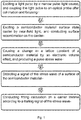
The method for testing the lifetime of the surface state carrier of the semiconductor, including the following steps: - 1) using a narrow pulse light source with photon energy higher than a semiconductor forbidden band width to emit a light pulse, coupling the light pulse to an interior of a near-field optical probe through light path collimation, and producing, by the near-field optical probe, a photon-generated carrier on a surface of a semiconductor material under test through excitation;
- 2) concentrating the excited photon-generated carrier on the surface of the semiconductor material, and conducting recombination continuously with a surface state as a recombination center, wherein a recombination rate is in direct proportion to a carrier concentration and a carrier lifetime;
- 3) in both carrier excitation and recombination processes in step 1) and step 2), producing a change in a lattice constant due to an electronic volume effect, producing a stress wave, and detecting a signal of the stress wave in a high-frequency broadband ultrasonic testing mode; and
- 4) conducting fitting calculation on the signal of the stress wave to obtain the lifetime of the surface state carrier τc .
- In the step 1), a width of the light pulse emitted by the narrow pulse light source is femtosecond-magnitude to nanosecond-magnitude, and is not more than 5 nanoseconds.
- In the step 1), the near-field optical probe is a near-field optical probe with a hole or a near-field optical probe without the hole, and the light pulse is coupled to an interior of the near-field optical probe with the hole or a surface of the near-field optical probe without the hole through collimation.
- In the step 1), a distance between the near-field optical probe and the surface of the semiconductor material under test is not more than 1/10 of a wave length of the light pulse.
- In the step 1), the photon-generated carrier excited by the near-field optical probe is located at a surface and a subsurface of a semiconductor under test.
- In the step 2), when the recombination of the photon-generated carrier, excited by the near-field optical probe, on the surface of the semiconductor under test is conducted, indirect recombination is conducted with the surface state as the center.
- In the step 2), the photon-generated carrier still conducts the recombination continuously after light pulse irradiation is finished, till the carrier in the semiconductor material is returned to a balance state.
- In the step 3), the signal of the stress wave of the surface of the semiconductor material is detected by means of a high-frequency broadband ultrasonic testing instrument, wherein the high-frequency broadband ultrasonic testing instrument includes an ultrasonic transducer, a laser doppler vibrometer, and a laser interferometer which have a nanosecond resolution.
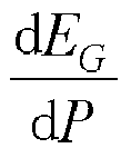
- In the step 4), fitting is conducted on a trailing part of the signal of the stress wave produced on the surface of the semiconductor material through excitation by near-field light to obtain the lifetime of the surface state carrier τc , wherein a specific fitting formula is:

- Compared with the prior art, the present invention has the following advantages that:
the present invention uses the near-field light to irradiate the surface of the semiconductor material to mainly excite the photon-generated carrier on the surface, uses the high-frequency ultrasonic transducer, the laser doppler vibrometer, and the laser interferometer which have the nanosecond resolution to detect the stress wave produced on the surface, can obtain the lifetime of the surface state carrier of the semiconductor after fitting calculation, can eliminate semiconductor bulk recombination influence, and has great significance for a solar cell, an integrated circuit chip, etc. -
-
Fig. 1 is a flow diagram of a method for testing a lifetime of a surface state carrier of a semiconductor of the present invention. -
Fig. 2 is a signal of a semiconductor surface state photon-generated stress wave and a fitting result. - The present invention is described in detail with reference to the drawings and the specific embodiments below.
- As shown in
Figs. 1 and2 , the present invention provides a method for testing a lifetime of a surface state carrier of a semiconductor, that is, a novel method for representing a dynamical property of a carrier in a surface state of the semiconductor, which can eliminate semiconductor bulk recombination influence, focuses on measuring the lifetime of the surface state carrier, and has great significance for a solar cell, an integrated circuit chip, etc. - Specifically, the method includes the following steps that:
- 1) a narrow pulse light source with photon energy higher than a semiconductor forbidden band width is used to emit a light pulse, the light pulse is coupled to an interior of a near-field optical probe through light path collimation, and near-field light excites an electron-hole pair on a surface of a semiconductor material under test, which is also called a photon-generated carrier, wherein a width of the light pulse emitted by the narrow pulse light source is femtosecond-magnitude to nanosecond-magnitude;
- 2) the photon-generated carrier excited in step 1) is concentrated on the surface of the semiconductor material, and recombination is conducted continuously with a surface state as a recombination center, wherein a recombination rate is in direct proportion to a carrier concentration and a carrier lifetime; the photon-generated carrier still conducts the recombination continuously after light pulse irradiation is finished, till the carrier in the semiconductor material is returned to a balance state;
- 3) in both carrier excitation and recombination processes in step 1) and step 2), a change in a lattice constant c is produced due to an electronic volume effect, wherein a relative change amount thereof is in direct proportion to an electron-hole pair concentration n;

- 4) according to a formula

Claims (9)
- A method for testing a lifetime of a surface state carrier of a semiconductor, comprising the following steps:1) using a narrow pulse light source with photon energy higher than a semiconductor forbidden band width to emit a light pulse, coupling the light pulse to an interior of a near-field optical probe through light path collimation, and producing, by the near-field optical probe, a photon-generated carrier on a surface of a semiconductor material under test through excitation;2) concentrating the excited photon-generated carrier on the surface of the semiconductor material, and conducting recombination continuously with a surface state as a recombination center, wherein a recombination rate is in direct proportion to a carrier concentration and a carrier lifetime;3) in both carrier excitation and recombination processes in step 1) and step 2), producing a change in a lattice constant due to an electronic volume effect, producing a stress wave, and detecting a signal of the stress wave in a high-frequency broadband ultrasonic testing mode; and4) conducting fitting calculation on the signal of the stress wave to obtain the lifetime of the surface state carrier τc .
- The method for testing the lifetime of the surface state carrier of the semiconductor according to claim 1, characterized in that in the step 1), a width of the light pulse emitted by the narrow pulse light source is femtosecond-magnitude to nanosecond-magnitude, and is not more than 5 nanoseconds.
- The method for testing the lifetime of the surface state carrier of the semiconductor according to claim 1, characterized in that in the step 1), the near-field optical probe is a near-field optical probe with a hole or a near-field optical probe without the hole, and the light pulse is coupled to an interior of the near-field optical probe with the hole or a surface of the near-field optical probe without the hole through collimation.
- The method for testing the lifetime of the surface state carrier of the semiconductor according to claim 1, characterized in that in the step 1), a distance between the near-field optical probe and the surface of the semiconductor material under test is not more than 1/10 of a wave length of the light pulse.
- The method for testing the lifetime of the surface state carrier of the semiconductor according to claim 1, characterized in that in the step 1), the photon-generated carrier excited by the near-field optical probe is located at a surface and a subsurface of a semiconductor under test.
- The method for testing the lifetime of the surface state carrier of the semiconductor according to claim 1, characterized in that in the step 2), when the recombination of the photon-generated carrier, excited by the near-field optical probe, on the surface of the semiconductor under test is conducted, indirect recombination is conducted with the surface state as the center.
- The method for testing the lifetime of the surface state carrier of the semiconductor according to claim 1, characterized in that in the step 2), the photon-generated carrier still conducts the recombination continuously after light pulse irradiation is finished, till the carrier in the semiconductor material is returned to a balance state.
- The method for testing the lifetime of the surface state carrier of the semiconductor according to claim 1, characterized in that in the step 3), the signal of the stress wave of the surface of the semiconductor material is detected by means of a high-frequency broadband ultrasonic testing instrument, wherein the high-frequency broadband ultrasonic testing instrument comprises an ultrasonic transducer, a laser doppler vibrometer, and a laser interferometer which have a nanosecond resolution.
- The method for testing the lifetime of the surface state carrier of the semiconductor according to claim 1, characterized in that in the step 4), fitting is conducted on a trailing part of the signal of the stress wave produced on the surface of the semiconductor material through excitation by near-field light to obtain the lifetime of the surface state carrier τc , wherein a specific fitting formula is:


Applications Claiming Priority (2)
| Application Number | Priority Date | Filing Date | Title |
|---|---|---|---|
| CN201910615736.2A CN110470965B (en) | 2019-07-09 | 2019-07-09 | A kind of semiconductor surface state carrier lifetime test method |
| PCT/CN2020/100429 WO2021004430A1 (en) | 2019-07-09 | 2020-07-06 | Semiconductor surface state carrier lifetime testing method |
Publications (3)
| Publication Number | Publication Date |
|---|---|
| EP3839529A1 true EP3839529A1 (en) | 2021-06-23 |
| EP3839529A4 EP3839529A4 (en) | 2021-12-01 |
| EP3839529B1 EP3839529B1 (en) | 2022-04-27 |
Family
ID=68507179
Family Applications (1)
| Application Number | Title | Priority Date | Filing Date |
|---|---|---|---|
| EP20837186.4A Active EP3839529B1 (en) | 2019-07-09 | 2020-07-06 | Semiconductor surface state carrier lifetime testing method |
Country Status (6)
| Country | Link |
|---|---|
| US (1) | US11719739B2 (en) |
| EP (1) | EP3839529B1 (en) |
| JP (1) | JP7271013B2 (en) |
| KR (1) | KR102643912B1 (en) |
| CN (1) | CN110470965B (en) |
| WO (1) | WO2021004430A1 (en) |
Families Citing this family (8)
| Publication number | Priority date | Publication date | Assignee | Title |
|---|---|---|---|---|
| CN110470965B (en) * | 2019-07-09 | 2020-07-28 | 同济大学 | A kind of semiconductor surface state carrier lifetime test method |
| CN114113226B (en) * | 2021-11-12 | 2022-07-19 | 广东省科学院半导体研究所 | Method for determining existence of novel electronic surface state and application thereof |
| KR102764674B1 (en) * | 2022-01-28 | 2025-02-11 | 연세대학교 산학협력단 | Methods for monitoring defects of semiconductor structure and apparatus of the same |
| US12000866B2 (en) | 2022-04-20 | 2024-06-04 | Envigth Co., Ltd. | Detection unit, semiconductor film layer inspection apparatus including the same, and semiconductor film layer inspection method using the same |
| KR102604572B1 (en) * | 2022-04-20 | 2023-11-21 | (주) 엔지온 | An measuring unit for measuring electrical characteristic of semiconductor, an apparatus with the unit and a method for measuring electrical characteristic of semiconductor with the apparatus |
| FR3148090B1 (en) * | 2023-04-19 | 2025-03-21 | Commissariat Energie Atomique | Electric current measuring system and electric current detection device for such a system |
| CN119008770B (en) * | 2024-08-08 | 2025-02-07 | 中国科学院长春光学精密机械与物理研究所 | A pulsed laser induced bleaching method for semiconductor devices |
| CN120293480B (en) * | 2025-06-12 | 2025-09-16 | 晋城市光机电产业协调服务中心(晋城市光机电产业研究院) | A semiconductor laser life prediction method and system |
Family Cites Families (24)
| Publication number | Priority date | Publication date | Assignee | Title |
|---|---|---|---|---|
| JP2928395B2 (en) * | 1991-02-04 | 1999-08-03 | 松下電子工業株式会社 | Semiconductor device reliability test method |
| CN1063159A (en) * | 1992-01-23 | 1992-07-29 | 中国科学院上海技术物理研究所 | A new method to measure the lifetime of non-equilibrium carriers in semiconductors |
| US5453703A (en) * | 1993-11-29 | 1995-09-26 | Semitest Inc. | Method for determining the minority carrier surface recombination lifetime constant (ts of a specimen of semiconductor material |
| US6346821B1 (en) * | 1998-03-27 | 2002-02-12 | Infineon Technologies Ag | Method for nondestructive measurement of minority carrier diffusion length and minority carrier lifetime in semiconductor devices |
| US6873932B1 (en) * | 2002-12-20 | 2005-03-29 | Advanced Micro Devices, Inc. | Method and apparatus for predicting semiconductor device lifetime |
| JP5295924B2 (en) | 2009-10-06 | 2013-09-18 | 株式会社神戸製鋼所 | Semiconductor carrier lifetime measuring apparatus and method |
| JP5686348B2 (en) * | 2010-02-15 | 2015-03-18 | 国立大学法人東京農工大学 | Photoinduced carrier lifetime measurement method, light incidence efficiency measurement method, photoinduced carrier lifetime measurement device, and light incidence efficiency measurement device |
| CN101975815A (en) | 2010-09-21 | 2011-02-16 | 上海大学 | Measuring method of recombination center concentration and trap center concentration in solar-grade crystalline silicon |
| US9029801B2 (en) * | 2011-02-15 | 2015-05-12 | Ysystems, Ltd. | Apparatus and method for measuring a luminescent decay |
| JP6052536B2 (en) * | 2011-12-16 | 2016-12-27 | 国立大学法人東京農工大学 | Photoinduced carrier lifetime measuring apparatus and photoinduced carrier lifetime measuring method |
| JP5858833B2 (en) | 2012-03-16 | 2016-02-10 | 株式会社神戸製鋼所 | Semiconductor evaluation method and semiconductor evaluation apparatus |
| CN102621465B (en) | 2012-03-19 | 2015-01-07 | 中国科学院上海技术物理研究所 | Method for detecting minority carrier lifetime of semiconductor nanowire |
| CN103576066B (en) * | 2012-07-26 | 2017-05-10 | 中芯国际集成电路制造(上海)有限公司 | Method for measuring service life of hot carrier of semiconductor device |
| CN103901335B (en) * | 2014-04-22 | 2016-03-30 | 哈尔滨工业大学 | A kind of infrared polarization optical imagery detection method of semiconductor minority carrier lifetime distribution and system |
| CN104359737B (en) * | 2014-11-21 | 2017-08-25 | 中国科学院宁波材料技术与工程研究所 | The method of testing of crystalline silicon body minority carrier life time |
| CN104819938A (en) * | 2015-05-20 | 2015-08-05 | 吉林大学 | Surface photovoltage measuring method with combination of modulated light and non-modulated light |
| US10539538B2 (en) * | 2015-07-09 | 2020-01-21 | The Boeing Company | Laser ultrasound system and method for inspection of a contoured structure |
| CN106680687A (en) * | 2017-01-05 | 2017-05-17 | 浙江师范大学 | Precise measuring method of crystalline silicon body lifetime |
| EP3492910A1 (en) * | 2017-12-04 | 2019-06-05 | Nederlandse Organisatie voor toegepast- natuurwetenschappelijk onderzoek TNO | Subsurface inspection method and system |
| CN108051722A (en) * | 2017-12-22 | 2018-05-18 | 中国电子产品可靠性与环境试验研究所 | The lifetime estimation method and system of hot carrier injection effect |
| JP7000198B2 (en) * | 2018-02-16 | 2022-01-19 | 浜松ホトニクス株式会社 | Carrier life measuring method and carrier life measuring device |
| CN108983063A (en) | 2018-05-29 | 2018-12-11 | 中国计量大学 | The test method of crystal silicon solar batteries minority carrier life time |
| CN110470965B (en) | 2019-07-09 | 2020-07-28 | 同济大学 | A kind of semiconductor surface state carrier lifetime test method |
| US11346818B2 (en) * | 2020-05-22 | 2022-05-31 | Intel Corporation | Method, device and system for non-destructive detection of defects in a semiconductor die |
-
2019
- 2019-07-09 CN CN201910615736.2A patent/CN110470965B/en active Active
-
2020
- 2020-07-06 WO PCT/CN2020/100429 patent/WO2021004430A1/en not_active Ceased
- 2020-07-06 KR KR1020217037545A patent/KR102643912B1/en active Active
- 2020-07-06 US US17/275,674 patent/US11719739B2/en active Active
- 2020-07-06 EP EP20837186.4A patent/EP3839529B1/en active Active
- 2020-07-06 JP JP2021549890A patent/JP7271013B2/en active Active
Also Published As
| Publication number | Publication date |
|---|---|
| EP3839529A4 (en) | 2021-12-01 |
| EP3839529B1 (en) | 2022-04-27 |
| US20220043049A1 (en) | 2022-02-10 |
| US11719739B2 (en) | 2023-08-08 |
| JP2022521625A (en) | 2022-04-11 |
| CN110470965B (en) | 2020-07-28 |
| KR20220005496A (en) | 2022-01-13 |
| CN110470965A (en) | 2019-11-19 |
| KR102643912B1 (en) | 2024-03-05 |
| WO2021004430A1 (en) | 2021-01-14 |
| JP7271013B2 (en) | 2023-05-11 |
Similar Documents
| Publication | Publication Date | Title |
|---|---|---|
| US11719739B2 (en) | Method for testing lifetime of surface state carrier of semiconductor | |
| JP2022521625A5 (en) | ||
| CN103098194B (en) | Utilize the crystallinity evaluating apparatus of the thin film semiconductor of μ-PCD method | |
| Thomsen et al. | Picosecond acoustics as a non-destructive tool for the characterization of very thin films | |
| CN102401632B (en) | Laser assistance transformation using two-photon absorption | |
| CN107860716A (en) | A kind of lossless detection method and equipment of the elastic constant based on laser-ultrasound | |
| WO2018072660A1 (en) | Terahertz time-domain reflectometry system | |
| JPH03119745A (en) | Method and apparatus for detecting and measuring impurity in crystalline semicon- ductor wafer | |
| CN103543130A (en) | Method for eliminating system frequency response influence of semiconductor material characteristic measuring device in photocarrier radiation technology | |
| CN104634760B (en) | Testing device and testing method for optical thin film stress | |
| CN104568766A (en) | Detection device and detection method for hole capturing dynamics of surfaces of quantum dots | |
| CN112051248B (en) | Nonlinear measurement method of light yield of scintillation materials based on laser excitation | |
| JP2635732B2 (en) | Optical fiber sensing method | |
| JP5093795B2 (en) | Fluorescence lifetime measuring apparatus, film forming apparatus, and fluorescence lifetime measuring method | |
| CN103616649A (en) | Magnetic field sensor sensitivity tuning method based on fiber bragg grating laser | |
| CN120063667A (en) | Method for measuring non-radiative decay life of laser crystal | |
| CN113740265B (en) | Multielement material A n B x C 1-x Element proportion detection method | |
| JP2000002648A (en) | Method and apparatus for measurement of breakdown threshold value of fine particles as well as measuring apparatus for fine particles in liquid by using them | |
| CN110940635A (en) | Ultraviolet second-order nonlinear optical testing device and testing method | |
| JPS6242537Y2 (en) | ||
| JP2011054784A (en) | Quantitative analysis limit determination method in iron concentration analysis in boron-doped p-type silicon | |
| CN113702495B (en) | Laser electromagnetic two-in-one probe and nondestructive testing device comprising same | |
| Bindhu et al. | Pulsed photoacoustic technique to study nonlinear processes in liquids: Results in toluene | |
| CN107192933B (en) | A kind of semiconductor material carrier effective lifetime measurement method | |
| CN106370994A (en) | High-frequency photoconductivity decay method charge carrier life tester |
Legal Events
| Date | Code | Title | Description |
|---|---|---|---|
| STAA | Information on the status of an ep patent application or granted ep patent |
Free format text: STATUS: THE INTERNATIONAL PUBLICATION HAS BEEN MADE |
|
| PUAI | Public reference made under article 153(3) epc to a published international application that has entered the european phase |
Free format text: ORIGINAL CODE: 0009012 |
|
| STAA | Information on the status of an ep patent application or granted ep patent |
Free format text: STATUS: REQUEST FOR EXAMINATION WAS MADE |
|
| 17P | Request for examination filed |
Effective date: 20210315 |
|
| AK | Designated contracting states |
Kind code of ref document: A1 Designated state(s): AL AT BE BG CH CY CZ DE DK EE ES FI FR GB GR HR HU IE IS IT LI LT LU LV MC MK MT NL NO PL PT RO RS SE SI SK SM TR |
|
| A4 | Supplementary search report drawn up and despatched |
Effective date: 20211102 |
|
| RIC1 | Information provided on ipc code assigned before grant |
Ipc: G01N 29/24 20060101ALI20211026BHEP Ipc: G01N 29/04 20060101AFI20211026BHEP |
|
| REG | Reference to a national code |
Ref country code: DE Ref legal event code: R079 Ref document number: 602020002872 Country of ref document: DE Free format text: PREVIOUS MAIN CLASS: G01R0031260000 Ipc: G01N0029040000 |
|
| GRAP | Despatch of communication of intention to grant a patent |
Free format text: ORIGINAL CODE: EPIDOSNIGR1 |
|
| STAA | Information on the status of an ep patent application or granted ep patent |
Free format text: STATUS: GRANT OF PATENT IS INTENDED |
|
| RIC1 | Information provided on ipc code assigned before grant |
Ipc: G01N 21/17 20060101ALN20220209BHEP Ipc: G01R 31/265 20060101ALI20220209BHEP Ipc: G01R 31/26 20200101ALI20220209BHEP Ipc: G01N 29/24 20060101ALI20220209BHEP Ipc: G01N 29/04 20060101AFI20220209BHEP |
|
| DAV | Request for validation of the european patent (deleted) | ||
| DAX | Request for extension of the european patent (deleted) | ||
| GRAS | Grant fee paid |
Free format text: ORIGINAL CODE: EPIDOSNIGR3 |
|
| INTG | Intention to grant announced |
Effective date: 20220224 |
|
| GRAA | (expected) grant |
Free format text: ORIGINAL CODE: 0009210 |
|
| STAA | Information on the status of an ep patent application or granted ep patent |
Free format text: STATUS: THE PATENT HAS BEEN GRANTED |
|
| AK | Designated contracting states |
Kind code of ref document: B1 Designated state(s): AL AT BE BG CH CY CZ DE DK EE ES FI FR GB GR HR HU IE IS IT LI LT LU LV MC MK MT NL NO PL PT RO RS SE SI SK SM TR |
|
| REG | Reference to a national code |
Ref country code: GB Ref legal event code: FG4D |
|
| REG | Reference to a national code |
Ref country code: CH Ref legal event code: EP |
|
| REG | Reference to a national code |
Ref country code: DE Ref legal event code: R096 Ref document number: 602020002872 Country of ref document: DE |
|
| REG | Reference to a national code |
Ref country code: AT Ref legal event code: REF Ref document number: 1487306 Country of ref document: AT Kind code of ref document: T Effective date: 20220515 |
|
| REG | Reference to a national code |
Ref country code: IE Ref legal event code: FG4D |
|
| REG | Reference to a national code |
Ref country code: NL Ref legal event code: FP |
|
| REG | Reference to a national code |
Ref country code: LT Ref legal event code: MG9D |
|
| REG | Reference to a national code |
Ref country code: AT Ref legal event code: MK05 Ref document number: 1487306 Country of ref document: AT Kind code of ref document: T Effective date: 20220427 |
|
| PG25 | Lapsed in a contracting state [announced via postgrant information from national office to epo] |
Ref country code: SE Free format text: LAPSE BECAUSE OF FAILURE TO SUBMIT A TRANSLATION OF THE DESCRIPTION OR TO PAY THE FEE WITHIN THE PRESCRIBED TIME-LIMIT Effective date: 20220427 Ref country code: PT Free format text: LAPSE BECAUSE OF FAILURE TO SUBMIT A TRANSLATION OF THE DESCRIPTION OR TO PAY THE FEE WITHIN THE PRESCRIBED TIME-LIMIT Effective date: 20220829 Ref country code: NO Free format text: LAPSE BECAUSE OF FAILURE TO SUBMIT A TRANSLATION OF THE DESCRIPTION OR TO PAY THE FEE WITHIN THE PRESCRIBED TIME-LIMIT Effective date: 20220727 Ref country code: LT Free format text: LAPSE BECAUSE OF FAILURE TO SUBMIT A TRANSLATION OF THE DESCRIPTION OR TO PAY THE FEE WITHIN THE PRESCRIBED TIME-LIMIT Effective date: 20220427 Ref country code: HR Free format text: LAPSE BECAUSE OF FAILURE TO SUBMIT A TRANSLATION OF THE DESCRIPTION OR TO PAY THE FEE WITHIN THE PRESCRIBED TIME-LIMIT Effective date: 20220427 Ref country code: GR Free format text: LAPSE BECAUSE OF FAILURE TO SUBMIT A TRANSLATION OF THE DESCRIPTION OR TO PAY THE FEE WITHIN THE PRESCRIBED TIME-LIMIT Effective date: 20220728 Ref country code: FI Free format text: LAPSE BECAUSE OF FAILURE TO SUBMIT A TRANSLATION OF THE DESCRIPTION OR TO PAY THE FEE WITHIN THE PRESCRIBED TIME-LIMIT Effective date: 20220427 Ref country code: BG Free format text: LAPSE BECAUSE OF FAILURE TO SUBMIT A TRANSLATION OF THE DESCRIPTION OR TO PAY THE FEE WITHIN THE PRESCRIBED TIME-LIMIT Effective date: 20220727 Ref country code: AT Free format text: LAPSE BECAUSE OF FAILURE TO SUBMIT A TRANSLATION OF THE DESCRIPTION OR TO PAY THE FEE WITHIN THE PRESCRIBED TIME-LIMIT Effective date: 20220427 |
|
| PG25 | Lapsed in a contracting state [announced via postgrant information from national office to epo] |
Ref country code: RS Free format text: LAPSE BECAUSE OF FAILURE TO SUBMIT A TRANSLATION OF THE DESCRIPTION OR TO PAY THE FEE WITHIN THE PRESCRIBED TIME-LIMIT Effective date: 20220427 Ref country code: PL Free format text: LAPSE BECAUSE OF FAILURE TO SUBMIT A TRANSLATION OF THE DESCRIPTION OR TO PAY THE FEE WITHIN THE PRESCRIBED TIME-LIMIT Effective date: 20220427 Ref country code: LV Free format text: LAPSE BECAUSE OF FAILURE TO SUBMIT A TRANSLATION OF THE DESCRIPTION OR TO PAY THE FEE WITHIN THE PRESCRIBED TIME-LIMIT Effective date: 20220427 Ref country code: IS Free format text: LAPSE BECAUSE OF FAILURE TO SUBMIT A TRANSLATION OF THE DESCRIPTION OR TO PAY THE FEE WITHIN THE PRESCRIBED TIME-LIMIT Effective date: 20220827 |
|
| REG | Reference to a national code |
Ref country code: DE Ref legal event code: R097 Ref document number: 602020002872 Country of ref document: DE |
|
| PG25 | Lapsed in a contracting state [announced via postgrant information from national office to epo] |
Ref country code: SM Free format text: LAPSE BECAUSE OF FAILURE TO SUBMIT A TRANSLATION OF THE DESCRIPTION OR TO PAY THE FEE WITHIN THE PRESCRIBED TIME-LIMIT Effective date: 20220427 Ref country code: SK Free format text: LAPSE BECAUSE OF FAILURE TO SUBMIT A TRANSLATION OF THE DESCRIPTION OR TO PAY THE FEE WITHIN THE PRESCRIBED TIME-LIMIT Effective date: 20220427 Ref country code: RO Free format text: LAPSE BECAUSE OF FAILURE TO SUBMIT A TRANSLATION OF THE DESCRIPTION OR TO PAY THE FEE WITHIN THE PRESCRIBED TIME-LIMIT Effective date: 20220427 Ref country code: ES Free format text: LAPSE BECAUSE OF FAILURE TO SUBMIT A TRANSLATION OF THE DESCRIPTION OR TO PAY THE FEE WITHIN THE PRESCRIBED TIME-LIMIT Effective date: 20220427 Ref country code: EE Free format text: LAPSE BECAUSE OF FAILURE TO SUBMIT A TRANSLATION OF THE DESCRIPTION OR TO PAY THE FEE WITHIN THE PRESCRIBED TIME-LIMIT Effective date: 20220427 Ref country code: DK Free format text: LAPSE BECAUSE OF FAILURE TO SUBMIT A TRANSLATION OF THE DESCRIPTION OR TO PAY THE FEE WITHIN THE PRESCRIBED TIME-LIMIT Effective date: 20220427 Ref country code: CZ Free format text: LAPSE BECAUSE OF FAILURE TO SUBMIT A TRANSLATION OF THE DESCRIPTION OR TO PAY THE FEE WITHIN THE PRESCRIBED TIME-LIMIT Effective date: 20220427 |
|
| PG25 | Lapsed in a contracting state [announced via postgrant information from national office to epo] |
Ref country code: MC Free format text: LAPSE BECAUSE OF FAILURE TO SUBMIT A TRANSLATION OF THE DESCRIPTION OR TO PAY THE FEE WITHIN THE PRESCRIBED TIME-LIMIT Effective date: 20220427 |
|
| PLBE | No opposition filed within time limit |
Free format text: ORIGINAL CODE: 0009261 |
|
| STAA | Information on the status of an ep patent application or granted ep patent |
Free format text: STATUS: NO OPPOSITION FILED WITHIN TIME LIMIT |
|
| REG | Reference to a national code |
Ref country code: BE Ref legal event code: MM Effective date: 20220731 |
|
| PG25 | Lapsed in a contracting state [announced via postgrant information from national office to epo] |
Ref country code: AL Free format text: LAPSE BECAUSE OF FAILURE TO SUBMIT A TRANSLATION OF THE DESCRIPTION OR TO PAY THE FEE WITHIN THE PRESCRIBED TIME-LIMIT Effective date: 20220427 |
|
| 26N | No opposition filed |
Effective date: 20230130 |
|
| PG25 | Lapsed in a contracting state [announced via postgrant information from national office to epo] |
Ref country code: LU Free format text: LAPSE BECAUSE OF NON-PAYMENT OF DUE FEES Effective date: 20220706 |
|
| PG25 | Lapsed in a contracting state [announced via postgrant information from national office to epo] |
Ref country code: SI Free format text: LAPSE BECAUSE OF FAILURE TO SUBMIT A TRANSLATION OF THE DESCRIPTION OR TO PAY THE FEE WITHIN THE PRESCRIBED TIME-LIMIT Effective date: 20220427 Ref country code: BE Free format text: LAPSE BECAUSE OF NON-PAYMENT OF DUE FEES Effective date: 20220731 |
|
| PG25 | Lapsed in a contracting state [announced via postgrant information from national office to epo] |
Ref country code: IE Free format text: LAPSE BECAUSE OF NON-PAYMENT OF DUE FEES Effective date: 20220706 |
|
| PG25 | Lapsed in a contracting state [announced via postgrant information from national office to epo] |
Ref country code: IT Free format text: LAPSE BECAUSE OF FAILURE TO SUBMIT A TRANSLATION OF THE DESCRIPTION OR TO PAY THE FEE WITHIN THE PRESCRIBED TIME-LIMIT Effective date: 20220427 |
|
| REG | Reference to a national code |
Ref country code: CH Ref legal event code: PL |
|
| PG25 | Lapsed in a contracting state [announced via postgrant information from national office to epo] |
Ref country code: MK Free format text: LAPSE BECAUSE OF FAILURE TO SUBMIT A TRANSLATION OF THE DESCRIPTION OR TO PAY THE FEE WITHIN THE PRESCRIBED TIME-LIMIT Effective date: 20220427 Ref country code: CY Free format text: LAPSE BECAUSE OF FAILURE TO SUBMIT A TRANSLATION OF THE DESCRIPTION OR TO PAY THE FEE WITHIN THE PRESCRIBED TIME-LIMIT Effective date: 20220427 Ref country code: CH Free format text: LAPSE BECAUSE OF NON-PAYMENT OF DUE FEES Effective date: 20230731 |
|
| PG25 | Lapsed in a contracting state [announced via postgrant information from national office to epo] |
Ref country code: HU Free format text: LAPSE BECAUSE OF FAILURE TO SUBMIT A TRANSLATION OF THE DESCRIPTION OR TO PAY THE FEE WITHIN THE PRESCRIBED TIME-LIMIT; INVALID AB INITIO Effective date: 20200706 |
|
| PG25 | Lapsed in a contracting state [announced via postgrant information from national office to epo] |
Ref country code: MT Free format text: LAPSE BECAUSE OF FAILURE TO SUBMIT A TRANSLATION OF THE DESCRIPTION OR TO PAY THE FEE WITHIN THE PRESCRIBED TIME-LIMIT Effective date: 20220427 |
|
| PG25 | Lapsed in a contracting state [announced via postgrant information from national office to epo] |
Ref country code: BG Free format text: LAPSE BECAUSE OF FAILURE TO SUBMIT A TRANSLATION OF THE DESCRIPTION OR TO PAY THE FEE WITHIN THE PRESCRIBED TIME-LIMIT Effective date: 20220427 |
|
| PG25 | Lapsed in a contracting state [announced via postgrant information from national office to epo] |
Ref country code: BG Free format text: LAPSE BECAUSE OF FAILURE TO SUBMIT A TRANSLATION OF THE DESCRIPTION OR TO PAY THE FEE WITHIN THE PRESCRIBED TIME-LIMIT Effective date: 20220427 |
|
| PGFP | Annual fee paid to national office [announced via postgrant information from national office to epo] |
Ref country code: NL Payment date: 20250516 Year of fee payment: 6 |
|
| PGFP | Annual fee paid to national office [announced via postgrant information from national office to epo] |
Ref country code: GB Payment date: 20250515 Year of fee payment: 6 |
|
| PGFP | Annual fee paid to national office [announced via postgrant information from national office to epo] |
Ref country code: FR Payment date: 20250508 Year of fee payment: 6 |
|
| PGFP | Annual fee paid to national office [announced via postgrant information from national office to epo] |
Ref country code: DE Payment date: 20250514 Year of fee payment: 6 |
|
| PG25 | Lapsed in a contracting state [announced via postgrant information from national office to epo] |
Ref country code: TR Free format text: LAPSE BECAUSE OF FAILURE TO SUBMIT A TRANSLATION OF THE DESCRIPTION OR TO PAY THE FEE WITHIN THE PRESCRIBED TIME-LIMIT Effective date: 20220427 |