EP3836200A1 - Semiconductor integrated circuit and electronic instrument - Google Patents
Semiconductor integrated circuit and electronic instrument Download PDFInfo
- Publication number
- EP3836200A1 EP3836200A1 EP19847209.4A EP19847209A EP3836200A1 EP 3836200 A1 EP3836200 A1 EP 3836200A1 EP 19847209 A EP19847209 A EP 19847209A EP 3836200 A1 EP3836200 A1 EP 3836200A1
- Authority
- EP
- European Patent Office
- Prior art keywords
- wiring
- integrated circuit
- driver
- semiconductor integrated
- distance
- Prior art date
- Legal status (The legal status is an assumption and is not a legal conclusion. Google has not performed a legal analysis and makes no representation as to the accuracy of the status listed.)
- Granted
Links
Images








Classifications
-
- H—ELECTRICITY
- H10—SEMICONDUCTOR DEVICES; ELECTRIC SOLID-STATE DEVICES NOT OTHERWISE PROVIDED FOR
- H10D—INORGANIC ELECTRIC SEMICONDUCTOR DEVICES
- H10D84/00—Integrated devices formed in or on semiconductor substrates that comprise only semiconducting layers, e.g. on Si wafers or on GaAs-on-Si wafers
- H10D84/01—Manufacture or treatment
- H10D84/0123—Integrating together multiple components covered by H10D12/00 or H10D30/00, e.g. integrating multiple IGBTs
- H10D84/0126—Integrating together multiple components covered by H10D12/00 or H10D30/00, e.g. integrating multiple IGBTs the components including insulated gates, e.g. IGFETs
- H10D84/0149—Manufacturing their interconnections or electrodes, e.g. source or drain electrodes
-
- G—PHYSICS
- G06—COMPUTING OR CALCULATING; COUNTING
- G06F—ELECTRIC DIGITAL DATA PROCESSING
- G06F1/00—Details not covered by groups G06F3/00 - G06F13/00 and G06F21/00
- G06F1/04—Generating or distributing clock signals or signals derived directly therefrom
- G06F1/10—Distribution of clock signals, e.g. skew
-
- H—ELECTRICITY
- H10—SEMICONDUCTOR DEVICES; ELECTRIC SOLID-STATE DEVICES NOT OTHERWISE PROVIDED FOR
- H10D—INORGANIC ELECTRIC SEMICONDUCTOR DEVICES
- H10D84/00—Integrated devices formed in or on semiconductor substrates that comprise only semiconducting layers, e.g. on Si wafers or on GaAs-on-Si wafers
- H10D84/01—Manufacture or treatment
- H10D84/02—Manufacture or treatment characterised by using material-based technologies
- H10D84/03—Manufacture or treatment characterised by using material-based technologies using Group IV technology, e.g. silicon technology or silicon-carbide [SiC] technology
- H10D84/038—Manufacture or treatment characterised by using material-based technologies using Group IV technology, e.g. silicon technology or silicon-carbide [SiC] technology using silicon technology, e.g. SiGe
-
- H—ELECTRICITY
- H10—SEMICONDUCTOR DEVICES; ELECTRIC SOLID-STATE DEVICES NOT OTHERWISE PROVIDED FOR
- H10W—GENERIC PACKAGES, INTERCONNECTIONS, CONNECTORS OR OTHER CONSTRUCTIONAL DETAILS OF DEVICES COVERED BY CLASS H10
- H10W20/00—Interconnections in chips, wafers or substrates
- H10W20/40—Interconnections external to wafers or substrates, e.g. back-end-of-line [BEOL] metallisations or vias connecting to gate electrodes
- H10W20/41—Interconnections external to wafers or substrates, e.g. back-end-of-line [BEOL] metallisations or vias connecting to gate electrodes characterised by their conductive parts
- H10W20/427—Power or ground buses
-
- H—ELECTRICITY
- H10—SEMICONDUCTOR DEVICES; ELECTRIC SOLID-STATE DEVICES NOT OTHERWISE PROVIDED FOR
- H10W—GENERIC PACKAGES, INTERCONNECTIONS, CONNECTORS OR OTHER CONSTRUCTIONAL DETAILS OF DEVICES COVERED BY CLASS H10
- H10W20/00—Interconnections in chips, wafers or substrates
- H10W20/40—Interconnections external to wafers or substrates, e.g. back-end-of-line [BEOL] metallisations or vias connecting to gate electrodes
- H10W20/41—Interconnections external to wafers or substrates, e.g. back-end-of-line [BEOL] metallisations or vias connecting to gate electrodes characterised by their conductive parts
- H10W20/435—Cross-sectional shapes or dispositions of interconnections
Definitions
- the present disclosure relates to a semiconductor integrated circuit and an electronic apparatus, and more particularly, to a semiconductor integrated circuit and an electronic apparatus capable of having further improved performance.
- the present disclosure has been made in view of such a situation, and an object of the present disclosure is to be capable of further improving performance.
- a first embodiment of a wiring shape used in a semiconductor integrated circuit to which the present technology is applied will be described with reference to Figs. 1 to 10 .
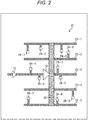
- a special wiring shape is often used, and for example, a so-called fishbone wiring shape as illustrated in Figs. 2 and 3 is used.
- Fig. 2 is a layout diagram illustrating a conventional wiring shape based on the circuit diagram illustrated in Fig. 1 .
- connection terminals 24-1 to 24-9 connected to the receivers 14-1 to 14-9 of Fig. 1 are provided on the branch lines 23-1 to 23-5. Furthermore, connection terminals 25-1 and 25-2 are also provided between a buffer 12 and the driver 13.
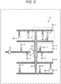
- Fig. 3 illustrates a layout diagram illustrating a wiring shape to which the present technology is applied, based on the circuit diagram illustrated in Fig. 1 .
- a clock wiring 31 illustrated in Fig. 3 has a fishbone wiring shape in which five branch lines 33-1 and 33-5 having a small wiring width are connected to a trunk line 32 having a large wiring width so as to be branched from the trunk line 32, similar to the clock wiring 21 of Fig. 2 .
- the clock wiring 31 of Fig. 3 has a layout in which the trunk line 32 is arranged along a vertical direction of a semiconductor integrated circuit.
- connection terminals 34-1 to 34-9 connected to the receivers 14-1 to 14-9 of Fig. 1 are provided on the branch lines 33-1 to 33-5. Furthermore, connection terminals 35-1 and 35-2 are also provided between a buffer 12 and the driver 13.
- an output terminal of the driver 13 is connected to the center of the trunk line 32, and the trunk line 32 has a wiring shape set so that a wiring width becomes smaller according to a distance from a connection portion of the driver 13 to upper and lower sides of the trunk line 32 in the vertical direction. That is, since a current density of a signal transmitted via the trunk line 32 decreases as a distance from the driver 13 increases, the wiring shape of the trunk line 32 is set so that the wiring width corresponds to the decrease in the current density.
- the trunk line 32 of which wiring width becomes small so as to be optimized according to the current density of the signal transmitted via the trunk line 32.
- Fig. 4 enlarges and illustrates an area surrounded by a broken line in Fig. 3 .
- the branch lines 33-1 and 33-2 illustrated in Fig. 4 have wiring shapes set so that wiring widths become smaller according to distances from branch portions with the trunk line 32 to the right in a horizontal direction, that is, as distances from the driver 13 increase, similar to the trunk line 32.
- the branch lines 33-1 and 33-2 extending from the trunk line 32 to the left also have wiring shapes set so that wiring widths become smaller according to distances from branch portions, and the same applies to the branch lines 33-3 to 33-5.
- performance of the semiconductor integrated circuit including the clock wiring 31 can be improved.
- a size of the driver 13 can be reduced, such that further power reduction becomes possible.
- the clock wiring 31 adopts the fishbone wiring shape such an effect can be obtained well.
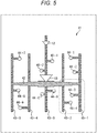
- Fig. 5 illustrates a layout diagram illustrating a wiring shape to which the present technology is applied, based on the circuit diagram illustrated in Fig. 1 , similar to Fig. 3 .
- Fig. 6 enlarges and illustrates an area surrounded by a broken line in Fig. 5 , similar to Fig. 4 .
- the trunk line 42 to which the driver 13 is connected has a wiring shape set so that a wiring width becomes smaller according to a distance from a connection portion of the driver 13 to the left and right in the horizontal direction.
- a branch line 43 branching from the trunk line 42 has a wiring shape set so that a wiring width becomes smaller according to a distance from a branch portion with the trunk line 42 to a lower side in the vertical direction, that is, as a distance from the driver 13 increases.
- the clock wiring 41 having such a wiring shape similar to the clock wiring 31 of Fig. 3 , better performance can be obtained by optimizing the wiring widths of the trunk line 42 and the branch line 43.
- Fig. 7 illustrates a specific wiring shape of the clock wiring 31 described with reference to Fig. 3 .
- the driver 13 is arranged at the center of gravity of the plurality of receivers 14 ( Fig. 1 ). Then, the driver 13 is connected to the trunk line 32 having a large wiring width via the through electrodes 51-1 to 51-3. Furthermore, the branch lines 33-1 to 33-4 having a small wiring width are connected to the trunk line 32 via through electrodes 52-1 to 52-4, respectively. Moreover, in the clock wiring 31, a plurality of VDD lines and a plurality of GND lines are arranged at regular intervals in parallel with the branch lines 33. Furthermore, the wiring shape of the clock wiring 31 is bilaterally symmetrical with respect to the center line of the trunk line 32.
- the wiring shape of the trunk line 32 is set so that the wiring width becomes gradually smaller so that a resistance increases toward a far end side, according to a change in the current density. Furthermore, the trunk line 32 is formed so that the wiring width becomes smaller by, for example, a predetermined constant width every constant distance from the connection portion of the driver 13.
- the wiring shape of the trunk line 32 is set so that the wiring width becomes smaller so as to be symmetrical with respect to the center line for every branch portion where the branch lines 33-1 to 33-3 are branched, from the connection portion of the driver 13 toward an upper side (similarly, toward a lower side (not illustrated)).
- the trunk line 32 is formed so that the wiring width changes from a wiring width D1 to a wiring width D2 ( ⁇ D1) at a branch portion where the branch line 33-3 is branched, changes from the wiring width D2 to a wiring width D3 ( ⁇ D2) at a branch portion where the branch line 33-2 is branched, and changes from the wiring width D3 to a wiring width D4 ( ⁇ D3) at a branch portion where the branch line 33-1 is branched.
- a wiring width D is formed so as to be symmetrical with respect to the center line, and will hereinafter be described as a width on one side with respect to the center line (that is, an actual wiring width is twice D), similar to Fig. 7 .
- a configuration example in which the driver 13 drives the clock wiring 31 of which total capacity including a wiring capacity and a gate capacity is 10 pF, a rate is controlled by Signal EM, a required wiring width on the driver 13 side is 5 ⁇ m, a total capacity (wiring capacity and gate capacity) connected to the receiver 14 is 0.1 pF, and a required wiring width on the receiver 14 side is 0.5 ⁇ m will be described.
- a drive charge decreases as the trunk line approaches the far end. Therefore, in a case where ten branch lines 33 are branched on one side of the trunk line 32 in a fishbone wiring shape as illustrated in Fig. 7 , it is preferable to set the wiring shape so that the wiring width of the trunk line 32 becomes smaller by 0.5 ⁇ m for every branch portion. Therefore, a redundant wiring capacity in the clock wiring 31 can be eliminated.
- Fig. 8 illustrates a modification of the wiring shape of the clock wiring 31 illustrated in Fig. 7 .
- branch lines 33A-1 to 33A-4 branched from the trunk line 32 have wiring shapes set so that wiring widths become smaller according to distances from the trunk line 32, that is, as distances from the driver 13 increase.
- a plurality of branch lines 33A forming the clock wiring 31A is formed so that the wiring widths become evenly smaller from the center line by a predetermined constant width every constant distance from branch portions from the trunk line 32.
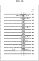
- Fig. 10 illustrates a specific wiring shape of the clock wiring 61 illustrated in B of Fig. 9 .
- the wiring width of the long-distance wiring 62 in a case of the wiring shape in which the wiring width becomes smaller according to the distance away from the connection portion of the driver 13, it is preferable to narrow the wiring width of the long-distance wiring 62 at a pitch of 10 ⁇ m to 100 ⁇ m and set the wiring shape so that the wiring width is a minimum width at a connection portion of the receiver 14.
- a length of the long-distance wiring 62 is about 100 ⁇ m to 15 mm
- it is possible to make the wiring shape optimal by calculating a wiring width required at the connection portion of the receiver 14, which is a far end, and gradually narrowing the wiring width from the driver 13 side with a value evenly divided so that the wiring width at the connection portion of the receiver 14 is the calculated wiring width.
- a wiring capacity is reduced, such that an amount of current can be reduced, power consumption can be reduced, and electro magnetic interference (EMI) characteristics can be improved.
- EMI electro magnetic interference
- a resistance value on the far end side increases, such that it is possible to reduce occurrence of reflection in a signal. Furthermore, areas of an upper layer wiring and a through electrode are reduced, such that antenna characteristics can also be improved. In particular, for a high-frequency clock in which the reflection of the signal easily occurs, a fine process in which electro migration (EM) is problematic, a large-scale wiring, or the like, better characteristics can be obtained.
- EM electro migration
- a second embodiment of a wiring shape used in a semiconductor integrated circuit to which the present technology is applied will be described with reference to Figs. 11 to 17 .
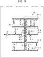
- Fig. 11 illustrates a layout diagram illustrating a wiring shape to which the present technology is applied, based on the circuit diagram illustrated in Fig. 1 .
- Fig. 12 enlarges and illustrates an area surrounded by a broken line in Fig. 11 .
- a clock wiring 81 illustrated in Figs. 11 and 12 has a fishbone wiring shape in which five branch lines 83-1 and 83-5 having a small wiring width are connected to a trunk line 82 having a large wiring width so as to be branched from the trunk line 82, similar to the clock wiring 21 of Fig. 2 .
- the clock wiring 81 of Fig. 11 has a layout in which the trunk line 82 is arranged along a vertical direction of a semiconductor integrated circuit.
- connection terminals 84-1 to 84-9 connected to the receivers 14-1 to 14-9 of Fig. 1 are provided on the branch lines 33-1 to 33-5. Furthermore, connection terminals 85-1 and 85-2 are also provided between a buffer 12 and a driver 13.
- a wiring shape of the trunk line 82 is set to be a mesh shape in which a plurality of slits is formed according to a frequency of the signal transmitted by the trunk line 82.
- the plurality of slits is formed in the trunk line 82 so as to become finer according to the frequency, such that it is possible to reduce the skin resistance component as the mesh shape in which a surface area of the trunk line 82 is increased.
- the wiring shape is set to be the mesh shape by forming the plurality of slits, such that a skin resistance can be reduced and attenuation of the signal can be suppressed. As a result, performance of the semiconductor integrated circuit including the clock wiring 81 can be improved.
- Fig. 13 illustrates a layout diagram illustrating a wiring shape to which the present technology is applied, based on the circuit diagram illustrated in Fig. 1 , similar to Fig. 11 .
- Fig. 14 enlarges and illustrates an area surrounded by a broken line in Fig. 13 , similar to Fig. 12 .
- a clock wiring 91 illustrated in Figs. 13 and 14 has a layout in which a trunk line 92 to which the driver 13 is connected is arranged along a horizontal direction of the semiconductor integrated circuit.
- a wiring shape of the trunk line 92 to which the driver 13 is connected is set to be a mesh shape in which a plurality of slits is formed according to a frequency of a signal transmitted by the trunk line 92.
- the clock wiring 91 having such a wiring shape similar to the clock wiring 81 of Fig. 11 , better performance can be obtained by forming the trunk line 92 in an optimum mesh shape according to the frequency of the signal.
- Fig. 15 illustrates a specific wiring shape of the clock wiring 81 described with reference to Fig. 11 .
- the driver 13 is connected to the trunk line 82 having a large wiring width via through electrodes 86-1 to 86-3.
- the branch lines 83-1 to 83-4 having a small wiring width are connected to the trunk line 82 via through electrodes 87-1 to 87-4, respectively.
- a plurality of VDD lines and a plurality of GND lines are arranged in parallel with the branch lines 33.
- the wiring shape of the clock wiring 81 is bilaterally symmetrical with respect to the center line of the trunk line 82.
- the slits having a width w and a height h are formed at a plurality of places of the trunk line 82, and the wiring shape of the trunk line 82 is set to be the mesh shape by these slits.
- the width w and the height h of the slit are formed to be smaller dimensions as the frequency of the signal transmitted by the clock wiring 81 becomes high, such that the trunk line 82 is formed in a finer mesh shape.
- a of Fig. 16 illustrates a circuit diagram of a long-distance wiring, as illustrated in A of Fig. 16 , an output terminal of the driver 13 is connected to an input terminal of the receiver 14 in a single wiring without providing a branch between the driver 13 and the receiver 14.
- the long-distance wiring 102 directed toward the vertical direction has a wiring shape set so that a plurality of slits is formed according to a frequency of a signal transmitted through the clock wiring 101, and is connected to the receiver 14. That is, in a case where the signal has a high frequency, the long-distance wiring 102 is formed to have a finer mesh shape so that a surface area increases by forming the slits.
- the long-distance wiring 112 directed toward the horizontal direction has a wiring shape set so that a plurality of slits is formed according to a frequency of a signal transmitted through the clock wiring 111, and is connected to the receiver 14. That is, in a case where the signal has a high frequency, the long-distance wiring 112 is formed to have a finer mesh shape so that a surface area increases by forming the slits.
- the driver 13 is connected to one end of the long-distance wiring 102 via a through electrode 103-1 and the receiver 14 is connected to the other end of the long-distance wiring 102 via a through electrode 103-2.
- the slits having a width w and a height h are formed at a plurality of places of the long-distance wiring 102, and the wiring shape of the long-distance wiring 102 is set to be the mesh shape by these slits. Therefore, a surface area of the long-distance wiring 102 can be increased, such that attenuation of the signal due to a skin resistance can be reduced.
- the width w and the height h of the slit are reduced, such that the wiring shape of the long-distance wiring 102 is set to be the finer mesh shape.
- a power supply wiring to which the present technology is applied will be described with reference to Fig. 18 .
- Fig. 18 illustrates a layout diagram of a power supply wiring.
- a power supply wiring 121 illustrated in Fig. 18 includes a current supply source 122 and a GND supply source 123, a VDD trunk line 124 is connected to the current supply source 122, and a GND trunk line 125 is connected to the GND supply source 123.
- the VDD trunk line 124 and the GND trunk line 125 having a large wiring width are arranged along the vertical direction of the semiconductor integrated circuit, and a plurality of VDD lines and a plurality of GND lines having a small wiring width are arranged along the horizontal direction of the semiconductor integrated circuit. Then, in the power supply wiring 121, the VDD trunk line 124 is connected to each of seven VDD lines via through electrodes 126-1 to 126-7, and the GND trunk line 125 is connected to each of six GND lines via through electrodes 127-1 to 127-6.
- a plurality of power consumption sources (for example, transistors) indicated by dot hatching is connected between VDD lines and GND lines at desired places.
- the VDD trunk line 124 is formed to have a larger wiring width for, for example, each of the plurality of power consumption sources each time the power consumption sources are connected.
- the power consumption sources are arranged so as to be dense at a place away from the current supply source 122, and the wiring shape of the VDD trunk line 124 is set so that the wiring width becomes larger toward the place.
- the GND trunk line 125 has a wiring shape set so that a wiring width becomes larger as a distance from the GND supply source 123 increases. That is, the GND trunk line 125 is formed so that the wiring width changes from a wiring width D21 to a wiring width D22 (> D21), changes from the wiring width D22 to a wiring width D23 (> D22), and changes from the wiring width D23 to a wiring width D24 (> D23), every constant distance from the GND supply source 123.
- the GND trunk line 125 is formed to have a larger wiring width for, for example, each of the plurality of power consumption sources each time the power consumption sources are connected.
- the power consumption sources are arranged so as to be dense at a place away from the GND supply source 123, and the wiring shape of the GND trunk line 125 is set so that the wiring width becomes larger toward the place.
- the power supply wiring 121 can realize an even voltage drop (IR Drop) along a longitudinal direction of the current supply source 122 and the GND supply source 123, and can improve resistance to an arrangement variation of the plurality of power consumption sources.
- the voltage drop can be made uniform, such that a jitter generated in a signal waveform can be improved or a signal timing can be improved, and better characteristics can resultantly be obtained.
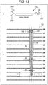
- Impedance matching will be described with reference to Fig. 19 .
- a of Fig. 19 illustrates a circuit diagram of a wiring for performing impedance matching.
- an output terminal of the driver 13 is grounded via a terminating resistor 132.
- the driver 13 is connected to one end of a signal line 133, which is a target for taking an impedance via a through electrode 134-1, and the terminating resistor 132 is connected to the other end of the signal line 133 via a through electrode 134-2.
- the signal line 133 is arranged along the vertical direction of the semiconductor integrated circuit, and a plurality of VDD lines and a plurality of GND lines are arranged along the horizontal direction of the semiconductor integrated circuit.
- the signal line 133 has a wiring shape set so that a wiring width becomes larger from the driver 13 toward the terminating resistor 132 so that the impedance is matched. That is, the signal line 133 is formed so that the wiring width changes from a wiring width D1 to a wiring width D2 (> D1) and changes from the wiring width D2 to a wiring width D3 (> D2), every constant distance from the driver 13.
- wiring resistors 142-1 to 142-5 from the driver 13 side to the receiver 14-5 are set to have the largest current density on the driver 13 side.
- a signal line 143 having a wiring shape in which a wiring width becomes large on the driver 13 side having a high current density and becomes small on the receiver 14-5 side having a low current density is adopted. That is, the signal line 143 is formed so that the wiring width changes from a wiring width D1 to a wiring width D2 ( ⁇ D1), changes from the wiring width D2 to a wiring width D3 ( ⁇ D2), changes from the wiring width D3 to a wiring width D4 ( ⁇ D3), and changes from the wiring width D4 to a wiring width D5 ( ⁇ D5), from the driver 13 for every connection portion where the receiver 14 is connected.
- the wiring width of the signal line is formed to become gradually smaller so that the resistance increases toward the far end side, such that reflection of a signal, electromagnetic radiation, or the like, can be reduced. Furthermore, in the semiconductor integrated circuit, the wiring width of the power supply wiring is formed to become gradually larger toward the far end side, such that an amount of voltage drop can be controlled, a more uniform voltage drop can be realized, and resistance to a variation can be improved.
- the semiconductor integrated circuit to which the wiring shape of each of the embodiments described above is applied can be applied to a design aiming at a high speed or a design aiming at low power consumption to realize further improvement of performance.
- the semiconductor integrated circuit can be more effective for a design requiring a high-speed (1 GHz or higher) clock or a large-scale (1 pF or higher) wiring.
- the present technology in a case where it is necessary to increase the wiring width due to severe EM or the like, in a case where a plurality of wirings should be used, or the like, by applying the present technology, an unnecessary wiring area can be reduced, such that an effect of reducing power consumption can be remarkably obtained. Furthermore, by applying the present technology to, for example, a high-frequency wiring of 1 GHz or higher, a wiring where the receiver 14 side is far away (for example, 3 mm or more), or the like, the wiring width of the wiring on the far end side can be minimized, such that an effect of reflection or noise suppression can be remarkably obtained.
- each of the embodiments as described above can be adopted in a semiconductor integrated circuit such as, for example, an imaging element, a signal processing circuit or the like, and can be applied to various electronic apparatuses such as, for example, an imaging system such as a digital still camera, a digital video camera or the like, a mobile phone having an imaging function, or another apparatus having an imaging function.
- a semiconductor integrated circuit such as, for example, an imaging element, a signal processing circuit or the like
- various electronic apparatuses such as, for example, an imaging system such as a digital still camera, a digital video camera or the like, a mobile phone having an imaging function, or another apparatus having an imaging function.
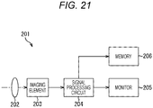
- Fig. 21 is a block diagram illustrating a configuration example of an imaging device mounted in an electronic apparatus.
- the imaging device 201 includes an optical system 202, an imaging element 203, a signal processing circuit 204, a monitor 205, and a memory 206, and can capture a still image and a moving image.
- the optical system 202 includes one or a plurality of lenses, guides image light (incident light) from a subject to the imaging element 203, and forms an image on a light receiving surface (sensor unit) of the imaging element 203.
- a semiconductor integrated circuit that has adopted the wiring shape described above is applied to the imaging element 203.
- the imaging element 203 electrons are accumulated for a certain period according to an image formed on the light receiving surface through the optical system 202. Then, a signal corresponding to the electrons accumulated in the imaging element 203 is supplied to the signal processing circuit 204.
- a semiconductor integrated circuit that has adopted the wiring shape described above is applied to the signal processing circuit 204, and the signal processing circuit 204 performs various signal processing on a pixel signal output from the imaging element 203.
- An image (image data) obtained by performing signal processing by the signal processing circuit 204 is supplied to and displayed on the monitor 205 or is supplied to and stored (recorded) in the memory 206.
- the imaging device 201 configured as described above, for example, power consumption can be reduced or reliability can be improved by applying the semiconductor integrated circuit that has adopted the wiring shape described above.
Landscapes
- Engineering & Computer Science (AREA)
- Theoretical Computer Science (AREA)
- Physics & Mathematics (AREA)
- General Engineering & Computer Science (AREA)
- General Physics & Mathematics (AREA)
- Design And Manufacture Of Integrated Circuits (AREA)
- Semiconductor Integrated Circuits (AREA)
- Internal Circuitry In Semiconductor Integrated Circuit Devices (AREA)
Abstract
Description
- The present disclosure relates to a semiconductor integrated circuit and an electronic apparatus, and more particularly, to a semiconductor integrated circuit and an electronic apparatus capable of having further improved performance.
- Generally, in a semiconductor integrated circuit, wirings configuring a wiring network (hereinafter referred to as the same net) through which the same signal is transmitted have a wiring shape designed to have the same wiring width. Furthermore, conventionally, wirings that have been attempted to be variously optimized have been proposed.
- For example,
Patent Document 1 proposes a wiring layout that minimizes a wiring delay by performing optimization in consideration of a wiring interval. Furthermore,Patent Document 2 proposes a clock wiring method for reducing clock skew by adjusting a length of adjacent wirings and non-uniformity of a wiring capacity due to intersection of interlayer wirings. -
- Patent Document 1: Japanese Patent Application Laid-Open No.
2002-313921 - Patent Document 2: Japanese Patent Application Laid-Open No.
2001-228931 - By the way, even in the same net, a variation in a current density occurs on one wiring, such that performance might be deteriorated in the wiring shape having the same wiring width. For example, in a case where the same wiring width is designed to be large, the performance is deteriorated in terms of power consumption, speed or the like due to an unnecessary wiring capacity.
- Note that since the wiring layout proposed in
Patent Document 1 described above is not a technology related to the same net and the clock wiring method proposed inPatent Document 2 is not a technology related to a wiring shape, such a problem could not be solved. - Therefore, it has been required to avoid the deterioration of the performance occurring in the conventional wiring shape, optimize the wiring shape in the same net, and improve performance of the semiconductor integrated circuit.
- The present disclosure has been made in view of such a situation, and an object of the present disclosure is to be capable of further improving performance.
- A semiconductor integrated circuit according to one aspect of the present disclosure includes: a wiring that forms a transmission network through which the same signal is transmitted; and a driver that supplies the signal to the wiring, in which the wiring has a wiring shape set according to a distance from the driver or a frequency of the signal.
- An electronic apparatus according to one aspect of the present disclosure includes: a semiconductor integrated circuit that includes: a wiring that forms a transmission network through which the same signal is transmitted; and a driver that supplies the signal to the wiring, in which the wiring has a wiring shape set according to a distance from the driver or a frequency of the signal.
- In one aspect of the present disclosure, a wiring that forms a transmission network through which the same signal is transmitted has a wiring shape set according to a distance from a driver that supplies the signal to the wiring or a frequency of the signal.
- According to one aspect of the present disclosure, it is possible to further improve the performance.
- Note that an effect described here is not necessarily limited, and may be any effect described in the present disclosure.
-
-
Fig. 1 is a diagram illustrating a circuit diagram of a clock wiring to which the present technology is applied. -
Fig. 2 is a layout diagram illustrating a conventional wiring shape. -
Fig. 3 is a layout diagram illustrating a wiring shape according to a first embodiment. -
Fig. 4 is an enlarged view of a part ofFig. 3 . -
Fig. 5 is a layout diagram illustrating another wiring shape according to the first embodiment. -
Fig. 6 is an enlarged view of a part ofFig. 5 . -
Fig. 7 is a diagram illustrating a specific configuration example of the wiring shape ofFig. 3 . -
Fig. 8 is a diagram illustrating a modification of the wiring shape illustrated inFig. 7 . -
Fig. 9 is a diagram for describing a wiring shape in which the first embodiment is applied to a long-distance wiring. -
Fig. 10 is a diagram illustrating a specific configuration example of the wiring shape ofFig. 9 . -
Fig. 11 is a layout diagram illustrating a wiring shape according to a second embodiment. -
Fig. 12 is an enlarged view of a part ofFig. 11 . -
Fig. 13 is a layout diagram illustrating another wiring shape according to the second embodiment. -
Fig. 14 is an enlarged view of a part ofFig. 13 . -
Fig. 15 is a diagram illustrating a specific configuration example of the wiring shape ofFig. 13 . -
Fig. 16 is a diagram for describing a wiring shape in which the second embodiment is applied to a long-distance wiring. -
Fig. 17 is a diagram illustrating a specific configuration example of the wiring shape ofFig. 16 . -
Fig. 18 is a layout diagram of a power supply wiring. -
Fig. 19 is a diagram for describing impedance matching. -
Fig. 20 is a diagram for describing occurrence of current concentration. -
Fig. 21 is a block diagram illustrating a configuration example of an electronic apparatus including a semiconductor integrated circuit. - Hereinafter, specific embodiments to which the present technology is applied will be described in detail with reference to the drawings.
- A first embodiment of a wiring shape used in a semiconductor integrated circuit to which the present technology is applied will be described with reference to
Figs. 1 to 10 . -
Fig. 1 illustrates a circuit diagram of a clock wiring to which the present technology is applied. - In a
clock wiring 11 illustrated inFig. 1 , signal lines of the same net are designed so that clock signals output from a clock generation circuit (not illustrated) are supplied to adriver 13 via buffers 12-1 and 12-2 and are supplied from thedriver 13 to a plurality ofreceivers 14. In an example illustrated inFig. 1 , a wiring shape of theclock wiring 11 is designed so that the signal lines are branched from an output terminal of thedriver 13 and are connected to input terminals of nine receivers 14-1 to 14-9. Then, drive elements 15-1 to 15-9 that drive according to the clock signal are connected to the receivers 14-1 to 14-9, respectively. - In such a
clock wiring 11, a special wiring shape is often used, and for example, a so-called fishbone wiring shape as illustrated inFigs. 2 and3 is used. -
Fig. 2 is a layout diagram illustrating a conventional wiring shape based on the circuit diagram illustrated inFig. 1 . - A
clock wiring 21 illustrated inFig. 2 has a fishbone wiring shape in which atrunk line 22, which is a signal line having a large wiring width, is connected to an output terminal of adriver 13 and branch lines 23, which are a plurality of signal lines having a small wiring width, are connected to thetrunk line 22 so as to be branched from thetrunk line 22. In an example illustrated inFig. 2 , five branch lines 23-1 to 23-5 are connected to thetrunk line 22. - Furthermore, in the
clock wiring 21, connection terminals 24-1 to 24-9 connected to the receivers 14-1 to 14-9 ofFig. 1 are provided on the branch lines 23-1 to 23-5. Furthermore, connection terminals 25-1 and 25-2 are also provided between abuffer 12 and thedriver 13. - Then, conventionally, in such a
clock wiring 21, thetrunk line 22 and the branch line 23 are designed so that wiring widths are constant. -
Fig. 3 illustrates a layout diagram illustrating a wiring shape to which the present technology is applied, based on the circuit diagram illustrated inFig. 1 . - A
clock wiring 31 illustrated inFig. 3 has a fishbone wiring shape in which five branch lines 33-1 and 33-5 having a small wiring width are connected to atrunk line 32 having a large wiring width so as to be branched from thetrunk line 32, similar to theclock wiring 21 ofFig. 2 . Note that theclock wiring 31 ofFig. 3 has a layout in which thetrunk line 32 is arranged along a vertical direction of a semiconductor integrated circuit. - Furthermore, in the
clock wiring 31, connection terminals 34-1 to 34-9 connected to the receivers 14-1 to 14-9 ofFig. 1 are provided on the branch lines 33-1 to 33-5. Furthermore, connection terminals 35-1 and 35-2 are also provided between abuffer 12 and thedriver 13. - Then, in the
clock wiring 31, an output terminal of thedriver 13 is connected to the center of thetrunk line 32, and thetrunk line 32 has a wiring shape set so that a wiring width becomes smaller according to a distance from a connection portion of thedriver 13 to upper and lower sides of thetrunk line 32 in the vertical direction. That is, since a current density of a signal transmitted via thetrunk line 32 decreases as a distance from thedriver 13 increases, the wiring shape of thetrunk line 32 is set so that the wiring width corresponds to the decrease in the current density. - Note that since the decrease in the current density changes not only according to the number of receivers, or the like, as well as the distance from the
driver 13, it is preferable to form thetrunk line 32 of which wiring width becomes small so as to be optimized according to the current density of the signal transmitted via thetrunk line 32. -
Fig. 4 enlarges and illustrates an area surrounded by a broken line inFig. 3 . - The branch lines 33-1 and 33-2 illustrated in
Fig. 4 have wiring shapes set so that wiring widths become smaller according to distances from branch portions with thetrunk line 32 to the right in a horizontal direction, that is, as distances from thedriver 13 increase, similar to thetrunk line 32. Of course, although not illustrated, the branch lines 33-1 and 33-2 extending from thetrunk line 32 to the left also have wiring shapes set so that wiring widths become smaller according to distances from branch portions, and the same applies to the branch lines 33-3 to 33-5. - As such, in the
clock wiring 31, thetrunk line 32 and the branch line 33 have the wiring shapes designed so that the wiring widths become smaller as the distances from thedriver 13 increase. Then, in theclock wiring 31, a wiring property can be improved by optimizing the wiring widths of thetrunk line 32 and the branch line 33. Therefore, theclock wiring 31 can reduce, for example, an unnecessary wiring capacity, and can avoid deterioration in performance in terms of power consumption, speed, or the like. Furthermore, in a case where thereceiver 14 that receives a signal is a complementary metal oxide semiconductor (CMOS), it is preferable to narrow the wiring widths of thetrunk line 32 and the branch line 33 so as to suppress reflection at end portions of thetrunk line 32 and the branch line 33. - As a result, performance of the semiconductor integrated circuit including the
clock wiring 31 can be improved. For example, in accordance with a reduction in a wiring capacity in theclock wiring 31, a size of thedriver 13 can be reduced, such that further power reduction becomes possible. In particular, in a case where theclock wiring 31 adopts the fishbone wiring shape, such an effect can be obtained well. -
Fig. 5 illustrates a layout diagram illustrating a wiring shape to which the present technology is applied, based on the circuit diagram illustrated inFig. 1 , similar toFig. 3 . Furthermore,Fig. 6 enlarges and illustrates an area surrounded by a broken line inFig. 5 , similar toFig. 4 . - A
clock wiring 41 illustrated inFigs. 5 and6 has a layout in which atrunk line 42 to which thedriver 13 is connected is arranged along the horizontal direction of the semiconductor integrated circuit. - Then, as illustrated in
Fig. 5 , in theclock wiring 41, similar to theclock wiring 31 ofFig. 3 , thetrunk line 42 to which thedriver 13 is connected has a wiring shape set so that a wiring width becomes smaller according to a distance from a connection portion of thedriver 13 to the left and right in the horizontal direction. Furthermore, as illustrated inFig. 6 , a branch line 43 branching from thetrunk line 42 has a wiring shape set so that a wiring width becomes smaller according to a distance from a branch portion with thetrunk line 42 to a lower side in the vertical direction, that is, as a distance from thedriver 13 increases. - In the
clock wiring 41 having such a wiring shape, similar to theclock wiring 31 ofFig. 3 , better performance can be obtained by optimizing the wiring widths of thetrunk line 42 and the branch line 43. -
Fig. 7 illustrates a specific wiring shape of theclock wiring 31 described with reference toFig. 3 . - In the
clock wiring 31 illustrated inFig. 7 , thedriver 13 is arranged at the center of gravity of the plurality of receivers 14 (Fig. 1 ). Then, thedriver 13 is connected to thetrunk line 32 having a large wiring width via the through electrodes 51-1 to 51-3. Furthermore, the branch lines 33-1 to 33-4 having a small wiring width are connected to thetrunk line 32 via through electrodes 52-1 to 52-4, respectively. Moreover, in theclock wiring 31, a plurality of VDD lines and a plurality of GND lines are arranged at regular intervals in parallel with the branch lines 33. Furthermore, the wiring shape of theclock wiring 31 is bilaterally symmetrical with respect to the center line of thetrunk line 32. - Then, since the current density decreases as the
trunk line 32 approaches a far end, as described above, the wiring shape of thetrunk line 32 is set so that the wiring width becomes gradually smaller so that a resistance increases toward a far end side, according to a change in the current density. Furthermore, thetrunk line 32 is formed so that the wiring width becomes smaller by, for example, a predetermined constant width every constant distance from the connection portion of thedriver 13. - For example, the wiring shape of the
trunk line 32 is set so that the wiring width becomes smaller so as to be symmetrical with respect to the center line for every branch portion where the branch lines 33-1 to 33-3 are branched, from the connection portion of thedriver 13 toward an upper side (similarly, toward a lower side (not illustrated)). That is, thetrunk line 32 is formed so that the wiring width changes from a wiring width D1 to a wiring width D2 (< D1) at a branch portion where the branch line 33-3 is branched, changes from the wiring width D2 to a wiring width D3 (< D2) at a branch portion where the branch line 33-2 is branched, and changes from the wiring width D3 to a wiring width D4 (< D3) at a branch portion where the branch line 33-1 is branched. Note that in the present embodiment, a wiring width D is formed so as to be symmetrical with respect to the center line, and will hereinafter be described as a width on one side with respect to the center line (that is, an actual wiring width is twice D), similar toFig. 7 . - Specifically, a configuration example in which the
driver 13 drives theclock wiring 31 of which total capacity including a wiring capacity and a gate capacity is 10 pF, a rate is controlled by Signal EM, a required wiring width on thedriver 13 side is 5 µm, a total capacity (wiring capacity and gate capacity) connected to thereceiver 14 is 0.1 pF, and a required wiring width on thereceiver 14 side is 0.5 µm will be described. In such a configuration example, a drive charge decreases as the trunk line approaches the far end. Therefore, in a case where ten branch lines 33 are branched on one side of thetrunk line 32 in a fishbone wiring shape as illustrated inFig. 7 , it is preferable to set the wiring shape so that the wiring width of thetrunk line 32 becomes smaller by 0.5 µm for every branch portion. Therefore, a redundant wiring capacity in theclock wiring 31 can be eliminated. - As such, conditions for appropriately eliminating the redundant wiring capacity of the
clock wiring 31 vary depending on layout situations, circuit situations or the like such as the wiring capacity or the gate capacity, the required wiring width, the number of branch lines 33, and the like. Therefore, it is necessary to appropriately design the wiring shape so as to narrow the wiring width of thetrunk line 32 according to those conditions. -
Fig. 8 illustrates a modification of the wiring shape of theclock wiring 31 illustrated inFig. 7 . - In a
clock wiring 31A illustrated inFig. 8 ,branch lines 33A-1 to 33A-4 branched from thetrunk line 32 have wiring shapes set so that wiring widths become smaller according to distances from thetrunk line 32, that is, as distances from thedriver 13 increase. For example, a plurality ofbranch lines 33A forming theclock wiring 31A is formed so that the wiring widths become evenly smaller from the center line by a predetermined constant width every constant distance from branch portions from thetrunk line 32. - For example, as illustrated in
Fig. 8 , thebranch lines 33A-1 to 33A-4 are formed so that the wiring widths become smaller every constant distance in the order of a length L1 from the center line of thetrunk line 32, a length L2 following the length L1, and a length L3 (L1 = L2 = L3) following the length L1. - As such, in the
clock wiring 31A, better performance can be obtained by optimizing the wiring widths of thetrunk line 32 and thebranch lines 33A. - A wiring shape in which the present technology is applied to a long-distance wiring will be described with reference to
Figs. 9 and10 . - A of
Fig. 9 illustrates a circuit diagram of a long-distance wiring. As illustrated in A ofFig. 9 , an output terminal of thedriver 13 is connected to an input terminal of thereceiver 14 and a distance between thedriver 13 and thereceiver 14 is greater than or equal to a predetermined distance, in a single wiring without providing a branch between thedriver 13 and thereceiver 14. - B of
Fig. 9 and C ofFig. 9 illustrate layout diagrams illustrating wiring shapes to which the present technology is applied, based on the circuit diagram illustrated in A ofFig. 9 . Furthermore, aclock wiring 61 of B ofFig. 9 has a layout in which a long-distance wiring 62 is arranged along the vertical direction of the semiconductor integrated circuit, and aclock wiring 71 of C ofFig. 9 has a layout in which a long-distance wiring 72 is arranged along the horizontal direction of the semiconductor integrated circuit. - As illustrated in B of
Fig. 9 , in theclock wiring 61, the long-distance wiring 62 has a wiring shape set so that a wiring width becomes smaller according to a distance from a connection portion of thedriver 13 to upper and lower sides in the vertical direction, and is connected to thereceiver 14. That is, since a current density of a signal transmitted via the long-distance wiring 62 decreases as a distance from thedriver 13 increases, the long-distance wiring 62 is formed so that the wiring width becomes smaller according to the decrease in the current density. - Similarly, as illustrated in C of
Fig. 9 , in theclock wiring 71, the long-distance wiring 72 has a wiring shape set so that a wiring width becomes smaller according to a distance from a connection portion of thedriver 13 to the left and right in the horizontal direction, and is connected to thereceiver 14. That is, since a current density of a signal transmitted via the long-distance wiring 72 decreases as a distance from thedriver 13 increases, the long-distance wiring 72 is formed so that the wiring width becomes smaller according to the decrease in the current density. - The clock wirings 61 and 71 having such wiring shapes are large-scale wirings using the long-
distance wirings receivers 14, a distance from thedriver 13 to thereceiver 14, or the like. -
Fig. 10 illustrates a specific wiring shape of theclock wiring 61 illustrated in B ofFig. 9 . - As illustrated in
Fig. 10 , thedriver 13 is connected to one end of the long-distance wiring 62 via a through electrode 63-1 and thereceiver 14 is connected to the other end of the long-distance wiring 62 via a through electrode 63-2. - Then, in the
clock wiring 61, the current density decreases as the long-distance wiring 62 approaches thereceiver 14, and the wiring shape of the long-distance wiring 62 is thus set so that the wiring width becomes smaller according to a change in the current density. For example, the wiring shape of the long-distance wiring 62 is set so that the wiring width becomes smaller so as to be symmetrical with respect to the center line from a connection portion of thedriver 13 toward an upper side. That is, the wiring shape of the long-distance wiring 62 is set so that the wiring width changes from a wiring width D1 to a wiring width D2 (< D1) and changes from the wiring width D2 to a wiring width D3 (< D2), according to a distance from thedriver 13. - Specifically, in a case of the wiring shape in which the wiring width becomes smaller according to the distance away from the connection portion of the
driver 13, it is preferable to narrow the wiring width of the long-distance wiring 62 at a pitch of 10 µm to 100 µm and set the wiring shape so that the wiring width is a minimum width at a connection portion of thereceiver 14. Alternatively, in a case where a length of the long-distance wiring 62 is about 100 µm to 15 mm, it is possible to make the wiring shape optimal by calculating a wiring width required at the connection portion of thereceiver 14, which is a far end, and gradually narrowing the wiring width from thedriver 13 side with a value evenly divided so that the wiring width at the connection portion of thereceiver 14 is the calculated wiring width. - By applying the wiring shape as described above, a wiring capacity is reduced, such that an amount of current can be reduced, power consumption can be reduced, and electro magnetic interference (EMI) characteristics can be improved.
- Furthermore, the wiring capacity can be reduced, such that a load capacity can be reduced, a speed can be improved, and a drive capacity of the
driver 13 can be reduced. As a result, power can be improved and an area can be reduced. Accordingly, the reduced area can be used for other wirings, such that a wiring property can be improved. - Moreover, by applying the wiring shape described above, a resistance value on the far end side increases, such that it is possible to reduce occurrence of reflection in a signal. Furthermore, areas of an upper layer wiring and a through electrode are reduced, such that antenna characteristics can also be improved. In particular, for a high-frequency clock in which the reflection of the signal easily occurs, a fine process in which electro migration (EM) is problematic, a large-scale wiring, or the like, better characteristics can be obtained.
- A second embodiment of a wiring shape used in a semiconductor integrated circuit to which the present technology is applied will be described with reference to
Figs. 11 to 17 . -
Fig. 11 illustrates a layout diagram illustrating a wiring shape to which the present technology is applied, based on the circuit diagram illustrated inFig. 1 . Furthermore,Fig. 12 enlarges and illustrates an area surrounded by a broken line inFig. 11 . - A
clock wiring 81 illustrated inFigs. 11 and12 has a fishbone wiring shape in which five branch lines 83-1 and 83-5 having a small wiring width are connected to atrunk line 82 having a large wiring width so as to be branched from thetrunk line 82, similar to theclock wiring 21 ofFig. 2 . Note that theclock wiring 81 ofFig. 11 has a layout in which thetrunk line 82 is arranged along a vertical direction of a semiconductor integrated circuit. - Furthermore, in the
clock wiring 81, connection terminals 84-1 to 84-9 connected to the receivers 14-1 to 14-9 ofFig. 1 are provided on the branch lines 33-1 to 33-5. Furthermore, connection terminals 85-1 and 85-2 are also provided between abuffer 12 and adriver 13. - Then, in the
clock wiring 81, in a case where an output terminal of thedriver 13 is connected to the center of thetrunk line 82 and a transmitted signal has a high frequency, a wiring shape of thetrunk line 82 is set to be a mesh shape in which a plurality of slits is formed according to a frequency of the signal transmitted by thetrunk line 82. - Generally, as the frequency of the signal transmitted by the
trunk line 82 becomes high, a ratio of a skin resistance component increases due to a direct current (DC) resistance. Therefore, in theclock wiring 81 via which a high-frequency signal is transmitted, the plurality of slits is formed in thetrunk line 82 so as to become finer according to the frequency, such that it is possible to reduce the skin resistance component as the mesh shape in which a surface area of thetrunk line 82 is increased. - Therefore, in the
clock wiring 81, the wiring shape is set to be the mesh shape by forming the plurality of slits, such that a skin resistance can be reduced and attenuation of the signal can be suppressed. As a result, performance of the semiconductor integrated circuit including theclock wiring 81 can be improved. -
Fig. 13 illustrates a layout diagram illustrating a wiring shape to which the present technology is applied, based on the circuit diagram illustrated inFig. 1 , similar toFig. 11 . Furthermore,Fig. 14 enlarges and illustrates an area surrounded by a broken line inFig. 13 , similar toFig. 12 . - A clock wiring 91 illustrated in
Figs. 13 and14 has a layout in which atrunk line 92 to which thedriver 13 is connected is arranged along a horizontal direction of the semiconductor integrated circuit. - Then, as illustrated in
Fig. 13 , in the clock wiring 91, similar to theclock wiring 81 ofFig. 11 , a wiring shape of thetrunk line 92 to which thedriver 13 is connected is set to be a mesh shape in which a plurality of slits is formed according to a frequency of a signal transmitted by thetrunk line 92. - In the clock wiring 91 having such a wiring shape, similar to the
clock wiring 81 ofFig. 11 , better performance can be obtained by forming thetrunk line 92 in an optimum mesh shape according to the frequency of the signal. -
Fig. 15 illustrates a specific wiring shape of theclock wiring 81 described with reference toFig. 11 . - In the
clock wiring 81 illustrated inFig. 15 , thedriver 13 is connected to thetrunk line 82 having a large wiring width via through electrodes 86-1 to 86-3. Furthermore, the branch lines 83-1 to 83-4 having a small wiring width are connected to thetrunk line 82 via through electrodes 87-1 to 87-4, respectively. Moreover, in theclock wiring 81, a plurality of VDD lines and a plurality of GND lines are arranged in parallel with the branch lines 33. Furthermore, the wiring shape of theclock wiring 81 is bilaterally symmetrical with respect to the center line of thetrunk line 82. - Then, as described above, the slits having a width w and a height h are formed at a plurality of places of the
trunk line 82, and the wiring shape of thetrunk line 82 is set to be the mesh shape by these slits. For example, the width w and the height h of the slit are formed to be smaller dimensions as the frequency of the signal transmitted by theclock wiring 81 becomes high, such that thetrunk line 82 is formed in a finer mesh shape. - A wiring shape in which the present technology is applied to a long-distance wiring will be described with reference to
Figs. 16 and17 . - A of
Fig. 16 illustrates a circuit diagram of a long-distance wiring, as illustrated in A ofFig. 16 , an output terminal of thedriver 13 is connected to an input terminal of thereceiver 14 in a single wiring without providing a branch between thedriver 13 and thereceiver 14. - B of
Fig. 16 and C ofFig. 16 illustrate layout diagrams illustrating wiring shapes to which the present technology is applied, based on the circuit diagram illustrated in A ofFig. 16 . Furthermore, aclock wiring 101 of B ofFig. 16 has a layout in which a long-distance wiring 102 is arranged along the vertical direction of the semiconductor integrated circuit, and aclock wiring 111 of C ofFig. 16 has a layout in which a long-distance wiring 112 is arranged along the horizontal direction of the semiconductor integrated circuit. - As illustrated in B of
Fig. 16 , in theclock wiring 101, the long-distance wiring 102 directed toward the vertical direction has a wiring shape set so that a plurality of slits is formed according to a frequency of a signal transmitted through theclock wiring 101, and is connected to thereceiver 14. That is, in a case where the signal has a high frequency, the long-distance wiring 102 is formed to have a finer mesh shape so that a surface area increases by forming the slits. - Similarly, as illustrated in C of
Fig. 17 , in theclock wiring 111, the long-distance wiring 112 directed toward the horizontal direction has a wiring shape set so that a plurality of slits is formed according to a frequency of a signal transmitted through theclock wiring 111, and is connected to thereceiver 14. That is, in a case where the signal has a high frequency, the long-distance wiring 112 is formed to have a finer mesh shape so that a surface area increases by forming the slits. - The clock wirings 101 and 111 having such wiring shapes are large-scale wirings using the long-
distance wirings receivers 14, a distance from thedriver 13 to thereceiver 14, or the like. -
Fig. 17 illustrates a specific wiring shape of theclock wiring 101 illustrated in B ofFig. 16 . - As illustrated in
Fig. 17 , thedriver 13 is connected to one end of the long-distance wiring 102 via a through electrode 103-1 and thereceiver 14 is connected to the other end of the long-distance wiring 102 via a through electrode 103-2. - Then, in the
clock wiring 101, the slits having a width w and a height h are formed at a plurality of places of the long-distance wiring 102, and the wiring shape of the long-distance wiring 102 is set to be the mesh shape by these slits. Therefore, a surface area of the long-distance wiring 102 can be increased, such that attenuation of the signal due to a skin resistance can be reduced. - For example, in the
clock wiring 101, as the frequency of the signal transmitted by the long-distance wiring 102 becomes high, the width w and the height h of the slit are reduced, such that the wiring shape of the long-distance wiring 102 is set to be the finer mesh shape. - By applying the wiring shape as described above, the skin resistance is reduced, such that the attenuation of the signal can be suppressed and a speed can be improved. Furthermore, a wiring capacity can be reduced, and power consumption can be reduced.
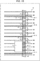
- A power supply wiring to which the present technology is applied will be described with reference to
Fig. 18 . -
Fig. 18 illustrates a layout diagram of a power supply wiring. - A
power supply wiring 121 illustrated inFig. 18 includes acurrent supply source 122 and aGND supply source 123, aVDD trunk line 124 is connected to thecurrent supply source 122, and aGND trunk line 125 is connected to theGND supply source 123. - Furthermore, the
VDD trunk line 124 and theGND trunk line 125 having a large wiring width are arranged along the vertical direction of the semiconductor integrated circuit, and a plurality of VDD lines and a plurality of GND lines having a small wiring width are arranged along the horizontal direction of the semiconductor integrated circuit. Then, in thepower supply wiring 121, theVDD trunk line 124 is connected to each of seven VDD lines via through electrodes 126-1 to 126-7, and theGND trunk line 125 is connected to each of six GND lines via through electrodes 127-1 to 127-6. - Furthermore, in an example illustrated in
Fig. 18 , a plurality of power consumption sources (for example, transistors) indicated by dot hatching is connected between VDD lines and GND lines at desired places. - In such a
power supply wiring 121, theVDD trunk line 124 has a wiring shape set so that a wiring width becomes larger as a distance from thecurrent supply source 122 increases. That is, theVDD trunk line 124 is formed so that the wiring width changes from a wiring width D11 to a wiring width D12 (> D11), changes from the wiring width D12 to a wiring width D13 (> D12), and changes from the wiring width D13 to a wiring width D14 (> D13), every constant distance from thecurrent supply source 122. - Furthermore, the
VDD trunk line 124 is formed to have a larger wiring width for, for example, each of the plurality of power consumption sources each time the power consumption sources are connected. In the example illustrated inFig. 18 , the power consumption sources are arranged so as to be dense at a place away from thecurrent supply source 122, and the wiring shape of theVDD trunk line 124 is set so that the wiring width becomes larger toward the place. - Similarly, in the
power supply wiring 121, theGND trunk line 125 has a wiring shape set so that a wiring width becomes larger as a distance from theGND supply source 123 increases. That is, theGND trunk line 125 is formed so that the wiring width changes from a wiring width D21 to a wiring width D22 (> D21), changes from the wiring width D22 to a wiring width D23 (> D22), and changes from the wiring width D23 to a wiring width D24 (> D23), every constant distance from theGND supply source 123. - Furthermore, the
GND trunk line 125 is formed to have a larger wiring width for, for example, each of the plurality of power consumption sources each time the power consumption sources are connected. In the example illustrated inFig. 18 , the power consumption sources are arranged so as to be dense at a place away from theGND supply source 123, and the wiring shape of theGND trunk line 125 is set so that the wiring width becomes larger toward the place. - Therefore, the
power supply wiring 121 can realize an even voltage drop (IR Drop) along a longitudinal direction of thecurrent supply source 122 and theGND supply source 123, and can improve resistance to an arrangement variation of the plurality of power consumption sources. - By applying the wiring shape as described above, the voltage drop can be made uniform, such that a jitter generated in a signal waveform can be improved or a signal timing can be improved, and better characteristics can resultantly be obtained.
- Impedance matching will be described with reference to
Fig. 19 . - A of
Fig. 19 illustrates a circuit diagram of a wiring for performing impedance matching. - As illustrated of A in
Fig. 19 , in awiring 131, an output terminal of thedriver 13 is grounded via a terminatingresistor 132. - As illustrated in B of
Fig. 19 , thedriver 13 is connected to one end of asignal line 133, which is a target for taking an impedance via a through electrode 134-1, and the terminatingresistor 132 is connected to the other end of thesignal line 133 via a through electrode 134-2. Furthermore, as illustrated in B ofFig. 19 , thesignal line 133 is arranged along the vertical direction of the semiconductor integrated circuit, and a plurality of VDD lines and a plurality of GND lines are arranged along the horizontal direction of the semiconductor integrated circuit. - Then, the
signal line 133 has a wiring shape set so that a wiring width becomes larger from thedriver 13 toward the terminatingresistor 132 so that the impedance is matched. That is, thesignal line 133 is formed so that the wiring width changes from a wiring width D1 to a wiring width D2 (> D1) and changes from the wiring width D2 to a wiring width D3 (> D2), every constant distance from thedriver 13. - Therefore, in the
wiring 131, impedance matching can be performed by thesignal line 133 so that an output impedance of thedriver 13 and an input impedance of the terminatingresistor 132 become equal to each other. - By applying the wiring shape as described above, electromagnetic radiation can be suppressed and reflection of a signal can be reduced, such that reliability can be improved, and better characteristics can resultantly be obtained.
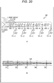
- An example in which current concentration occurs will be described with reference to
Fig. 20 . - In a
wiring 141 as illustrated in A ofFig. 20 , if current densities on adriver 13 side and receiver 14-1 to 14-5 sides are compared with each other, the current density is higher on thedriver 13 side than on the receiver 14-1 to 14-5 sides. Therefore, it is preferable that wiring resistors 142-1 to 142-5 from thedriver 13 side to the receiver 14-5 are set to have the largest current density on thedriver 13 side. - Therefore, as illustrated in B of
Fig. 20 , in thewiring 141, asignal line 143 having a wiring shape in which a wiring width becomes large on thedriver 13 side having a high current density and becomes small on the receiver 14-5 side having a low current density is adopted. That is, thesignal line 143 is formed so that the wiring width changes from a wiring width D1 to a wiring width D2 (< D1), changes from the wiring width D2 to a wiring width D3 (< D2), changes from the wiring width D3 to a wiring width D4 (< D3), and changes from the wiring width D4 to a wiring width D5 (< D5), from thedriver 13 for every connection portion where thereceiver 14 is connected. - By adopting such a wiring shape, it is possible to reduce a redundant wiring capacity in the
wiring 141. - As described above, in the semiconductor integrated circuit to which the wiring shape of each of the embodiments described above is applied, the wiring width of the signal line is formed to become gradually smaller so that the resistance increases toward the far end side, such that reflection of a signal, electromagnetic radiation, or the like, can be reduced. Furthermore, in the semiconductor integrated circuit, the wiring width of the power supply wiring is formed to become gradually larger toward the far end side, such that an amount of voltage drop can be controlled, a more uniform voltage drop can be realized, and resistance to a variation can be improved.
- Furthermore, the semiconductor integrated circuit to which the wiring shape of each of the embodiments described above is applied can be applied to a design aiming at a high speed or a design aiming at low power consumption to realize further improvement of performance. For example, the semiconductor integrated circuit can be more effective for a design requiring a high-speed (1 GHz or higher) clock or a large-scale (1 pF or higher) wiring.
- Moreover, in the future, as miniaturization of the semiconductor integrated circuit progresses, a wiring becomes thinner and film thinning progresses, such that there is concern about adverse effects such as EM, high resistance or the like, but by applying the wiring shape of each of the embodiments described above, it is possible to suppress those adverse effects. Similarly, due to the progress of the miniaturization, there is a concern about an adverse effect of a variation, and in particular, it is assumed that the uniformity of the voltage drop in the power consumption source (for example, the transistor) as described with reference to
FIG. 18 is emphasized, and thus, it is very effective to be able to make the voltage drop uniform as described above. - In particular, for example, in a case where it is necessary to increase the wiring width due to severe EM or the like, in a case where a plurality of wirings should be used, or the like, by applying the present technology, an unnecessary wiring area can be reduced, such that an effect of reducing power consumption can be remarkably obtained. Furthermore, by applying the present technology to, for example, a high-frequency wiring of 1 GHz or higher, a wiring where the
receiver 14 side is far away (for example, 3 mm or more), or the like, the wiring width of the wiring on the far end side can be minimized, such that an effect of reflection or noise suppression can be remarkably obtained. - The wiring shape of each of the embodiments as described above can be adopted in a semiconductor integrated circuit such as, for example, an imaging element, a signal processing circuit or the like, and can be applied to various electronic apparatuses such as, for example, an imaging system such as a digital still camera, a digital video camera or the like, a mobile phone having an imaging function, or another apparatus having an imaging function.
-
Fig. 21 is a block diagram illustrating a configuration example of an imaging device mounted in an electronic apparatus. - As illustrated in
Fig. 21 , theimaging device 201 includes anoptical system 202, animaging element 203, asignal processing circuit 204, amonitor 205, and amemory 206, and can capture a still image and a moving image. - The
optical system 202 includes one or a plurality of lenses, guides image light (incident light) from a subject to theimaging element 203, and forms an image on a light receiving surface (sensor unit) of theimaging element 203. - A semiconductor integrated circuit that has adopted the wiring shape described above is applied to the
imaging element 203. In theimaging element 203, electrons are accumulated for a certain period according to an image formed on the light receiving surface through theoptical system 202. Then, a signal corresponding to the electrons accumulated in theimaging element 203 is supplied to thesignal processing circuit 204. - A semiconductor integrated circuit that has adopted the wiring shape described above is applied to the
signal processing circuit 204, and thesignal processing circuit 204 performs various signal processing on a pixel signal output from theimaging element 203. An image (image data) obtained by performing signal processing by thesignal processing circuit 204 is supplied to and displayed on themonitor 205 or is supplied to and stored (recorded) in thememory 206. - In the
imaging device 201 configured as described above, for example, power consumption can be reduced or reliability can be improved by applying the semiconductor integrated circuit that has adopted the wiring shape described above. - Note that the present technology can also have the following configuration.
- (1) A semiconductor integrated circuit including:
- a wiring that forms a transmission network through which the same signal is transmitted; and
- a driver that supplies the signal to the wiring,
- in which the wiring has a wiring shape set according to a distance from the driver or a frequency of the signal.
- (2) The semiconductor integrated circuit according to the above (1),
in which the wiring has a wiring shape set so that a wiring width becomes smaller as the distance from the driver increases. - (3) The semiconductor integrated circuit according to the above (1) or (2),
in which the wiring width of the wiring becomes small so as to suppress reflection of the signal at an end portion of the wiring in a case where a receiver receiving the signal is a complementary metal oxide semiconductor (CMOS). - (4) The semiconductor integrated circuit according to any one of the above (1) to (3),
in which the wiring has a wiring shape set so that the wiring width is in accordance with a current density of the signal. - (5) The semiconductor integrated circuit according to any one of the above (1) to (4),
in which the transmission network is formed by a first wiring to which the driver is connected and which has a large wiring width and a plurality of second wirings which is branched from the first wiring and has a small wiring width, and
the first wiring has a wiring shape set so that a wiring width becomes smaller for every branch portion of the second wirings as a distance from a connection portion of the driver increases. - (6) The semiconductor integrated circuit according to the above (5),
in which the first wiring has a central portion to which the driver is connected, and has a wiring width that becomes smaller so that a resistance increases toward a far end side. - (7) The semiconductor integrated circuit according to the above (5) or (6),
in which the first wiring is formed so that the wiring width becomes smaller by a predetermined constant width every constant distance from the connection portion of the driver. - (8) The semiconductor integrated circuit according to any one of the above (5) to (7),
in which the second wiring is formed so that the wiring width becomes smaller by a predetermined constant width every constant distance from the branch portion from the first wiring. - (9) The semiconductor integrated circuit according to the above (1) or (2),
in which the wiring is a long-distance wiring that singly connects the driver to the receiver and has a predetermined distance or more. - (10) The semiconductor integrated circuit according to any one of the above (1) to (9),
in which the wiring has a wiring shape set to be a mesh shape by forming a plurality of slits in a case where the signal has a high frequency. - (11) The semiconductor integrated circuit according to the above (10),
in which the wiring is formed in the mesh shape so that the slits become finer as the frequency of the signal increases. - (12) The semiconductor integrated circuit according to the above (10) or (11),
in which the wiring is a long-distance wiring that singly connects the driver to the receiver and has a predetermined distance or more. - (13) The semiconductor integrated circuit according to any one of the above (1) to (12),
in which the wiring is a power supply wiring that supplies power from a current supply source to a plurality of power consumption sources, and has a wiring shape set so that a wiring width becomes larger as a distance from the current supply source increases. - (14) The semiconductor integrated circuit according to the above (13),
in which the wiring is formed to have a larger wiring width for each of a plurality of the power consumption sources, each time the power consumption sources are connected. - (15) The semiconductor integrated circuit according to any one of the above (1) to (14),
in which the wiring has a wiring shape set so that a wiring width becomes larger from the driver toward a terminating resistor so that an impedance is matched. - (16) The semiconductor integrated circuit according to the above (15),
in which the wiring width of the wiring becomes large by a predetermined constant width every constant distance from the driver. - (17) An electronic apparatus including:
a semiconductor integrated circuit that includes:- a wiring that forms a transmission network through which the same signal is transmitted; and
- a driver that supplies the signal to the wiring,
- in which the wiring has a wiring shape set according to a distance from the driver or a frequency of the signal.
- Note that the present embodiment is not limited to the embodiment described above, and various modifications can be made without departing from the scope of the present disclosure. Furthermore, effects described in the present specification are merely examples and are not limited, and other effects may be provided.
-
- 11
- Clock wiring
- 12
- Buffer
- 13
- Driver
- 14
- Receiver
- 15
- Drive element
- 31
- Clock wiring
- 32
- Trunk line
- 33
- Branch line
- 34 and 35
- Connection terminal
- 41
- Clock wiring
- 42
- Trunk line
- 43
- Branch line
- 44 and 45
- Connection terminal
- 51 and 52
- Through electrode
- 61
- Clock wiring
- 62
- Long-distance wiring
- 63
- Through electrode
- 71
- Clock wiring
- 72
- Long-distance wiring
- 81
- Clock wiring
- 82
- Trunk line
- 83
- Branch line
- 84 and 85
- Connection terminal
- 86 and 87
- Through electrode
- 91
- Clock wiring
- 92
- Trunk line
- 93
- Branch line
- 94 and 95
- Connection terminal
- 101
- Clock wiring
- 102
- Long-distance wiring
- 103
- Through electrode
- 111
- Clock wiring
- 112
- Long-distance wiring
- 121
- Power supply wiring
- 122
- Current supply source
- 123
- GND supply source
- 124
- VDD trunk line
- 125
- GND trunk line
- 126 and 127
- Through electrode
- 131
- Wiring
- 132
- Terminating resistor
- 133
- Signal line
- 134
- Through electrode
- 141
- Wiring
- 142
- Wiring resistor
- 143
- Wiring
Claims (17)
- A semiconductor integrated circuit comprising:a wiring that forms a transmission network through which the same signal is transmitted; anda driver that supplies the signal to the wiring,wherein the wiring has a wiring shape set according to a distance from the driver or a frequency of the signal.
- The semiconductor integrated circuit according to claim 1,
wherein the wiring has a wiring shape set so that a wiring width becomes smaller as the distance from the driver increases. - The semiconductor integrated circuit according to claim 2,
wherein the wiring width of the wiring becomes small so as to suppress reflection of the signal at an end portion of the wiring in a case where a receiver receiving the signal is a complementary metal oxide semiconductor (CMOS). - The semiconductor integrated circuit according to claim 2,
wherein the wiring has a wiring shape set so that the wiring width is in accordance with a current density of the signal. - The semiconductor integrated circuit according to claim 2,
wherein the transmission network is formed by a first wiring to which the driver is connected and which has a large wiring width and a plurality of second wirings which is branched from the first wiring and has a small wiring width, and
the first wiring has a wiring shape set so that a wiring width becomes smaller for every branch portion of the second wirings as a distance from a connection portion of the driver increases. - The semiconductor integrated circuit according to claim 5,
wherein the first wiring has a central portion to which the driver is connected, and has a wiring width that becomes smaller so that a resistance increases toward a far end side. - The semiconductor integrated circuit according to claim 5,
wherein the first wiring is formed so that the wiring width becomes smaller by a predetermined constant width every constant distance from the connection portion of the driver. - The semiconductor integrated circuit according to claim 5,
wherein the second wiring is formed so that the wiring width becomes smaller by a predetermined constant width every constant distance from the branch portion from the first wiring. - The semiconductor integrated circuit according to claim 2,
wherein the wiring is a long-distance wiring that singly connects the driver to the receiver and has a predetermined distance or more. - The semiconductor integrated circuit according to claim 1,
wherein the wiring has a wiring shape set to be a mesh shape by forming a plurality of slits in a case where the signal has a high frequency. - The semiconductor integrated circuit according to claim 10,
wherein the wiring is formed in the mesh shape so that the slits become finer as the frequency of the signal increases. - The semiconductor integrated circuit according to claim 10,
wherein the wiring is a long-distance wiring that singly connects the driver to the receiver and has a predetermined distance or more. - The semiconductor integrated circuit according to claim 1,
wherein the wiring is a power supply wiring that supplies power from a current supply source to a plurality of power consumption sources, and has a wiring shape set so that a wiring width becomes larger as a distance from the current supply source increases. - The semiconductor integrated circuit according to claim 13,
wherein the wiring is formed to have a larger wiring width for each of a plurality of the power consumption sources, each time the power consumption sources are connected. - The semiconductor integrated circuit according to claim 1,
wherein the wiring has a wiring shape set so that a wiring width becomes larger from the driver toward a terminating resistor so that an impedance is matched. - The semiconductor integrated circuit according to claim 15,
wherein the wiring width of the wiring becomes large by a predetermined constant width every constant distance from the driver. - An electronic apparatus comprising:
a semiconductor integrated circuit that includes:a wiring that forms a transmission network through which the same signal is transmitted; anda driver that supplies the signal to the wiring,wherein the wiring has a wiring shape set according to a distance from the driver or a frequency of the signal.
Applications Claiming Priority (2)
| Application Number | Priority Date | Filing Date | Title |
|---|---|---|---|
| JP2018150466A JP2021182567A (en) | 2018-08-09 | 2018-08-09 | Semiconductor integrated circuits and electronic devices |
| PCT/JP2019/029367 WO2020031743A1 (en) | 2018-08-09 | 2019-07-26 | Semiconductor integrated circuit and electronic instrument |
Publications (3)
| Publication Number | Publication Date |
|---|---|
| EP3836200A1 true EP3836200A1 (en) | 2021-06-16 |
| EP3836200A4 EP3836200A4 (en) | 2022-01-26 |
| EP3836200B1 EP3836200B1 (en) | 2025-07-23 |
Family
ID=69415223
Family Applications (1)
| Application Number | Title | Priority Date | Filing Date |
|---|---|---|---|
| EP19847209.4A Active EP3836200B1 (en) | 2018-08-09 | 2019-07-26 | Semiconductor integrated circuit and electronic instrument |
Country Status (5)
| Country | Link |
|---|---|
| US (1) | US20210265269A1 (en) |
| EP (1) | EP3836200B1 (en) |
| JP (1) | JP2021182567A (en) |
| CN (1) | CN112534568B (en) |
| WO (1) | WO2020031743A1 (en) |
Family Cites Families (15)
| Publication number | Priority date | Publication date | Assignee | Title |
|---|---|---|---|---|
| JPH02224370A (en) * | 1989-02-27 | 1990-09-06 | Hitachi Ltd | Semiconductor integrated circuit device |
| JP3026387B2 (en) * | 1991-08-23 | 2000-03-27 | 沖電気工業株式会社 | Semiconductor integrated circuit |
| JP3129864B2 (en) * | 1992-05-08 | 2001-01-31 | 株式会社東芝 | Wiring shape and wiring route determination method |
| JP2000200114A (en) * | 1999-01-07 | 2000-07-18 | Nec Corp | Clock distribution circuit |
| JP3471277B2 (en) | 2000-02-17 | 2003-12-02 | 沖電気工業株式会社 | Clock driver circuit and clock wiring method |
| JP2002313921A (en) | 2001-04-19 | 2002-10-25 | Matsushita Electric Ind Co Ltd | Wiring layout design method for semiconductor integrated circuit |
| US7531752B2 (en) * | 2003-07-24 | 2009-05-12 | Nec Corporation | Flexible substrate and electronic device |
| US7291923B1 (en) * | 2003-07-24 | 2007-11-06 | Xilinx, Inc. | Tapered signal lines |
| US7615841B2 (en) * | 2005-05-02 | 2009-11-10 | Taiwan Semiconductor Manufacturing Company, Ltd. | Design structure for coupling noise prevention |
| US20080256380A1 (en) * | 2007-04-16 | 2008-10-16 | Masanori Tsutsumi | Semiconductor integrated circuit and layout method for the same |
| JP5051836B2 (en) * | 2007-09-28 | 2012-10-17 | ルネサスエレクトロニクス株式会社 | Semiconductor device and design method thereof |
| JP2011055302A (en) * | 2009-09-02 | 2011-03-17 | Panasonic Corp | High frequency transmission line |
| JP2012019063A (en) * | 2010-07-08 | 2012-01-26 | Renesas Electronics Corp | Semiconductor device |
| US10157254B2 (en) * | 2015-12-29 | 2018-12-18 | Taiwan Semiconductor Manufacturing Co., Ltd. | Techniques based on electromigration characteristics of cell interconnect |
| JPWO2017122417A1 (en) * | 2016-01-12 | 2018-11-08 | ソニー株式会社 | Integrated circuit |
-
2018
- 2018-08-09 JP JP2018150466A patent/JP2021182567A/en active Pending
-
2019
- 2019-07-26 EP EP19847209.4A patent/EP3836200B1/en active Active
- 2019-07-26 WO PCT/JP2019/029367 patent/WO2020031743A1/en not_active Ceased
- 2019-07-26 US US17/260,753 patent/US20210265269A1/en not_active Abandoned
- 2019-07-26 CN CN201980051589.9A patent/CN112534568B/en active Active
Also Published As
| Publication number | Publication date |
|---|---|
| CN112534568B (en) | 2025-02-28 |
| JP2021182567A (en) | 2021-11-25 |
| EP3836200B1 (en) | 2025-07-23 |
| EP3836200A4 (en) | 2022-01-26 |
| WO2020031743A1 (en) | 2020-02-13 |
| CN112534568A (en) | 2021-03-19 |
| US20210265269A1 (en) | 2021-08-26 |
Similar Documents
| Publication | Publication Date | Title |
|---|---|---|
| US7830221B2 (en) | Coupling cancellation scheme | |
| KR100423693B1 (en) | Liquid crystal display device | |
| US10158339B2 (en) | Capacitive compensation structures using partially meshed ground planes | |
| JP3993297B2 (en) | Control circuit | |
| US8797250B2 (en) | Liquid crystal display device, and timing controller and signal processing method used in same | |
| US20070096154A1 (en) | Standard cell | |
| US20200126470A1 (en) | Display panel and display device | |
| KR20110037339A (en) | Electronic device, display device and control method of display device | |
| EP2547096A2 (en) | Solid-state image sensing apparatus | |
| US20030173634A1 (en) | Solid image pickup apparatus | |
| US20050104673A1 (en) | Semiconductor integrated circuit | |
| CN114974119A (en) | Display panel and display device | |
| EP3836200B1 (en) | Semiconductor integrated circuit and electronic instrument | |
| KR100404258B1 (en) | Shield circuit and integrated circuit in which the shield circuit is used | |
| US6919619B2 (en) | Actively-shielded signal wires | |
| US20130009673A1 (en) | Adaptive body bias circuit and semiconductor integrated circuit including the same | |
| KR20040010710A (en) | Low power clock distribution methodology | |
| US9678530B2 (en) | Clock skew adjusting structure | |
| CN112820227B (en) | Gate drive circuit | |
| JP2000029923A (en) | Automatic placement and routing device and semiconductor integrated circuit | |
| US7750761B2 (en) | Signal transmission structure | |
| WO2017122417A1 (en) | Integrated circuit | |
| CN114783305B (en) | Display panel and display device | |
| JP2006086505A (en) | Circuit structure and circuit substrate for changing characteristic impedance using different reference surface | |
| KR102357489B1 (en) | Chip on film circuit board for reducing electromagnetic interference and display device having the same |
Legal Events
| Date | Code | Title | Description |
|---|---|---|---|
| STAA | Information on the status of an ep patent application or granted ep patent |
Free format text: STATUS: THE INTERNATIONAL PUBLICATION HAS BEEN MADE |
|
| PUAI | Public reference made under article 153(3) epc to a published international application that has entered the european phase |
Free format text: ORIGINAL CODE: 0009012 |
|
| STAA | Information on the status of an ep patent application or granted ep patent |
Free format text: STATUS: REQUEST FOR EXAMINATION WAS MADE |
|
| 17P | Request for examination filed |
Effective date: 20210305 |
|
| AK | Designated contracting states |
Kind code of ref document: A1 Designated state(s): AL AT BE BG CH CY CZ DE DK EE ES FI FR GB GR HR HU IE IS IT LI LT LU LV MC MK MT NL NO PL PT RO RS SE SI SK SM TR |
|
| RIC1 | Information provided on ipc code assigned before grant |
Ipc: H01L 23/528 20060101ALI20210917BHEP Ipc: H01L 21/8234 20060101ALI20210917BHEP Ipc: H01L 21/822 20060101ALI20210917BHEP Ipc: G06F 1/10 20060101AFI20210917BHEP |
|
| DAV | Request for validation of the european patent (deleted) | ||
| DAX | Request for extension of the european patent (deleted) | ||
| REG | Reference to a national code |
Ref country code: DE Ref legal event code: R079 Free format text: PREVIOUS MAIN CLASS: H01L0021820000 Ipc: G06F0001100000 Ref document number: 602019073012 Country of ref document: DE |
|
| A4 | Supplementary search report drawn up and despatched |
Effective date: 20220103 |
|
| RIC1 | Information provided on ipc code assigned before grant |
Ipc: H01L 23/528 20060101ALI20211220BHEP Ipc: H01L 21/8234 20060101ALI20211220BHEP Ipc: H01L 21/822 20060101ALI20211220BHEP Ipc: G06F 1/10 20060101AFI20211220BHEP |
|
| STAA | Information on the status of an ep patent application or granted ep patent |
Free format text: STATUS: EXAMINATION IS IN PROGRESS |
|
| 17Q | First examination report despatched |
Effective date: 20230306 |
|
| GRAP | Despatch of communication of intention to grant a patent |
Free format text: ORIGINAL CODE: EPIDOSNIGR1 |
|
| STAA | Information on the status of an ep patent application or granted ep patent |
Free format text: STATUS: GRANT OF PATENT IS INTENDED |
|
| INTG | Intention to grant announced |
Effective date: 20241108 |
|
| GRAJ | Information related to disapproval of communication of intention to grant by the applicant or resumption of examination proceedings by the epo deleted |
Free format text: ORIGINAL CODE: EPIDOSDIGR1 |
|
| STAA | Information on the status of an ep patent application or granted ep patent |
Free format text: STATUS: EXAMINATION IS IN PROGRESS |
|
| GRAP | Despatch of communication of intention to grant a patent |
Free format text: ORIGINAL CODE: EPIDOSNIGR1 |
|
| STAA | Information on the status of an ep patent application or granted ep patent |
Free format text: STATUS: GRANT OF PATENT IS INTENDED |
|
| GRAJ | Information related to disapproval of communication of intention to grant by the applicant or resumption of examination proceedings by the epo deleted |
Free format text: ORIGINAL CODE: EPIDOSDIGR1 |
|
| STAA | Information on the status of an ep patent application or granted ep patent |
Free format text: STATUS: EXAMINATION IS IN PROGRESS |
|
| GRAP | Despatch of communication of intention to grant a patent |
Free format text: ORIGINAL CODE: EPIDOSNIGR1 |
|
| STAA | Information on the status of an ep patent application or granted ep patent |
Free format text: STATUS: GRANT OF PATENT IS INTENDED |
|
| INTG | Intention to grant announced |
Effective date: 20250210 |
|
| RIC1 | Information provided on ipc code assigned before grant |
Ipc: H10D 84/03 20250101ALI20250131BHEP Ipc: H10D 84/01 20250101ALI20250131BHEP Ipc: H01L 23/528 20060101ALI20250131BHEP Ipc: G06F 1/10 20060101AFI20250131BHEP |
|
| INTC | Intention to grant announced (deleted) | ||
| INTG | Intention to grant announced |
Effective date: 20250221 |
|
| GRAS | Grant fee paid |
Free format text: ORIGINAL CODE: EPIDOSNIGR3 |
|
| GRAA | (expected) grant |
Free format text: ORIGINAL CODE: 0009210 |
|
| STAA | Information on the status of an ep patent application or granted ep patent |
Free format text: STATUS: THE PATENT HAS BEEN GRANTED |
|
| P01 | Opt-out of the competence of the unified patent court (upc) registered |
Free format text: CASE NUMBER: APP_24089/2025 Effective date: 20250520 |
|
| AK | Designated contracting states |
Kind code of ref document: B1 Designated state(s): AL AT BE BG CH CY CZ DE DK EE ES FI FR GB GR HR HU IE IS IT LI LT LU LV MC MK MT NL NO PL PT RO RS SE SI SK SM TR |
|
| REG | Reference to a national code |
Ref country code: GB Ref legal event code: FG4D |
|
| REG | Reference to a national code |
Ref country code: CH Ref legal event code: EP |
|
| REG | Reference to a national code |
Ref country code: DE Ref legal event code: R096 Ref document number: 602019073012 Country of ref document: DE |
|
| REG | Reference to a national code |
Ref country code: IE Ref legal event code: FG4D |
|
| REG | Reference to a national code |
Ref country code: NL Ref legal event code: FP |
|
| PGFP | Annual fee paid to national office [announced via postgrant information from national office to epo] |
Ref country code: NL Payment date: 20250820 Year of fee payment: 7 |
|
| PGFP | Annual fee paid to national office [announced via postgrant information from national office to epo] |
Ref country code: DE Payment date: 20250820 Year of fee payment: 7 |
|
| PGFP | Annual fee paid to national office [announced via postgrant information from national office to epo] |
Ref country code: GB Payment date: 20250808 Year of fee payment: 7 |
|
| PG25 | Lapsed in a contracting state [announced via postgrant information from national office to epo] |
Ref country code: PT Free format text: LAPSE BECAUSE OF FAILURE TO SUBMIT A TRANSLATION OF THE DESCRIPTION OR TO PAY THE FEE WITHIN THE PRESCRIBED TIME-LIMIT Effective date: 20251124 |
|
| REG | Reference to a national code |
Ref country code: AT Ref legal event code: MK05 Ref document number: 1817062 Country of ref document: AT Kind code of ref document: T Effective date: 20250723 |
|
| PG25 | Lapsed in a contracting state [announced via postgrant information from national office to epo] |
Ref country code: IS Free format text: LAPSE BECAUSE OF FAILURE TO SUBMIT A TRANSLATION OF THE DESCRIPTION OR TO PAY THE FEE WITHIN THE PRESCRIBED TIME-LIMIT Effective date: 20251123 |
|
| PG25 | Lapsed in a contracting state [announced via postgrant information from national office to epo] |
Ref country code: NO Free format text: LAPSE BECAUSE OF FAILURE TO SUBMIT A TRANSLATION OF THE DESCRIPTION OR TO PAY THE FEE WITHIN THE PRESCRIBED TIME-LIMIT Effective date: 20251023 |
|
| REG | Reference to a national code |
Ref country code: LT Ref legal event code: MG9D |
|
| PG25 | Lapsed in a contracting state [announced via postgrant information from national office to epo] |
Ref country code: AT Free format text: LAPSE BECAUSE OF FAILURE TO SUBMIT A TRANSLATION OF THE DESCRIPTION OR TO PAY THE FEE WITHIN THE PRESCRIBED TIME-LIMIT Effective date: 20250723 |
|
| PG25 | Lapsed in a contracting state [announced via postgrant information from national office to epo] |
Ref country code: FI Free format text: LAPSE BECAUSE OF FAILURE TO SUBMIT A TRANSLATION OF THE DESCRIPTION OR TO PAY THE FEE WITHIN THE PRESCRIBED TIME-LIMIT Effective date: 20250723 |
|
| PG25 | Lapsed in a contracting state [announced via postgrant information from national office to epo] |
Ref country code: HR Free format text: LAPSE BECAUSE OF FAILURE TO SUBMIT A TRANSLATION OF THE DESCRIPTION OR TO PAY THE FEE WITHIN THE PRESCRIBED TIME-LIMIT Effective date: 20250723 |
|
| PG25 | Lapsed in a contracting state [announced via postgrant information from national office to epo] |
Ref country code: GR Free format text: LAPSE BECAUSE OF FAILURE TO SUBMIT A TRANSLATION OF THE DESCRIPTION OR TO PAY THE FEE WITHIN THE PRESCRIBED TIME-LIMIT Effective date: 20251024 |
|
| PG25 | Lapsed in a contracting state [announced via postgrant information from national office to epo] |
Ref country code: SE Free format text: LAPSE BECAUSE OF FAILURE TO SUBMIT A TRANSLATION OF THE DESCRIPTION OR TO PAY THE FEE WITHIN THE PRESCRIBED TIME-LIMIT Effective date: 20250723 |
|
| PG25 | Lapsed in a contracting state [announced via postgrant information from national office to epo] |
Ref country code: LV Free format text: LAPSE BECAUSE OF FAILURE TO SUBMIT A TRANSLATION OF THE DESCRIPTION OR TO PAY THE FEE WITHIN THE PRESCRIBED TIME-LIMIT Effective date: 20250723 |
|
| PG25 | Lapsed in a contracting state [announced via postgrant information from national office to epo] |
Ref country code: BG Free format text: LAPSE BECAUSE OF FAILURE TO SUBMIT A TRANSLATION OF THE DESCRIPTION OR TO PAY THE FEE WITHIN THE PRESCRIBED TIME-LIMIT Effective date: 20250723 Ref country code: PL Free format text: LAPSE BECAUSE OF FAILURE TO SUBMIT A TRANSLATION OF THE DESCRIPTION OR TO PAY THE FEE WITHIN THE PRESCRIBED TIME-LIMIT Effective date: 20250723 |
|
| PG25 | Lapsed in a contracting state [announced via postgrant information from national office to epo] |
Ref country code: RS Free format text: LAPSE BECAUSE OF FAILURE TO SUBMIT A TRANSLATION OF THE DESCRIPTION OR TO PAY THE FEE WITHIN THE PRESCRIBED TIME-LIMIT Effective date: 20251023 |
|
| PG25 | Lapsed in a contracting state [announced via postgrant information from national office to epo] |
Ref country code: ES Free format text: LAPSE BECAUSE OF FAILURE TO SUBMIT A TRANSLATION OF THE DESCRIPTION OR TO PAY THE FEE WITHIN THE PRESCRIBED TIME-LIMIT Effective date: 20250723 |
|
| REG | Reference to a national code |
Ref country code: CH Ref legal event code: H13 Free format text: ST27 STATUS EVENT CODE: U-0-0-H10-H13 (AS PROVIDED BY THE NATIONAL OFFICE) Effective date: 20260224 |
|
| PG25 | Lapsed in a contracting state [announced via postgrant information from national office to epo] |
Ref country code: LU Free format text: LAPSE BECAUSE OF NON-PAYMENT OF DUE FEES Effective date: 20250726 Ref country code: RO Free format text: LAPSE BECAUSE OF FAILURE TO SUBMIT A TRANSLATION OF THE DESCRIPTION OR TO PAY THE FEE WITHIN THE PRESCRIBED TIME-LIMIT Effective date: 20250723 |
|
| REG | Reference to a national code |
Ref country code: BE Ref legal event code: MM Effective date: 20250731 |
|
| PG25 | Lapsed in a contracting state [announced via postgrant information from national office to epo] |
Ref country code: SM Free format text: LAPSE BECAUSE OF FAILURE TO SUBMIT A TRANSLATION OF THE DESCRIPTION OR TO PAY THE FEE WITHIN THE PRESCRIBED TIME-LIMIT Effective date: 20250723 |
|
| PG25 | Lapsed in a contracting state [announced via postgrant information from national office to epo] |
Ref country code: DK Free format text: LAPSE BECAUSE OF FAILURE TO SUBMIT A TRANSLATION OF THE DESCRIPTION OR TO PAY THE FEE WITHIN THE PRESCRIBED TIME-LIMIT Effective date: 20250723 |
|
| PG25 | Lapsed in a contracting state [announced via postgrant information from national office to epo] |
Ref country code: IT Free format text: LAPSE BECAUSE OF FAILURE TO SUBMIT A TRANSLATION OF THE DESCRIPTION OR TO PAY THE FEE WITHIN THE PRESCRIBED TIME-LIMIT Effective date: 20250723 Ref country code: BE Free format text: LAPSE BECAUSE OF NON-PAYMENT OF DUE FEES Effective date: 20250731 |
|
| PG25 | Lapsed in a contracting state [announced via postgrant information from national office to epo] |
Ref country code: CZ Free format text: LAPSE BECAUSE OF FAILURE TO SUBMIT A TRANSLATION OF THE DESCRIPTION OR TO PAY THE FEE WITHIN THE PRESCRIBED TIME-LIMIT Effective date: 20250723 Ref country code: CH Free format text: LAPSE BECAUSE OF NON-PAYMENT OF DUE FEES Effective date: 20250731 |
|
| PG25 | Lapsed in a contracting state [announced via postgrant information from national office to epo] |
Ref country code: EE Free format text: LAPSE BECAUSE OF FAILURE TO SUBMIT A TRANSLATION OF THE DESCRIPTION OR TO PAY THE FEE WITHIN THE PRESCRIBED TIME-LIMIT Effective date: 20250723 Ref country code: SK Free format text: LAPSE BECAUSE OF FAILURE TO SUBMIT A TRANSLATION OF THE DESCRIPTION OR TO PAY THE FEE WITHIN THE PRESCRIBED TIME-LIMIT Effective date: 20250723 |