EP3829271A1 - Printed circuit board - Google Patents
Printed circuit board Download PDFInfo
- Publication number
- EP3829271A1 EP3829271A1 EP19841421.1A EP19841421A EP3829271A1 EP 3829271 A1 EP3829271 A1 EP 3829271A1 EP 19841421 A EP19841421 A EP 19841421A EP 3829271 A1 EP3829271 A1 EP 3829271A1
- Authority
- EP
- European Patent Office
- Prior art keywords
- electrodes
- electrode
- solder
- insulating substrate
- printed circuit
- Prior art date
- Legal status (The legal status is an assumption and is not a legal conclusion. Google has not performed a legal analysis and makes no representation as to the accuracy of the status listed.)
- Withdrawn
Links
Images



Classifications
-
- H—ELECTRICITY
- H05—ELECTRIC TECHNIQUES NOT OTHERWISE PROVIDED FOR
- H05K—PRINTED CIRCUITS; CASINGS OR CONSTRUCTIONAL DETAILS OF ELECTRIC APPARATUS; MANUFACTURE OF ASSEMBLAGES OF ELECTRICAL COMPONENTS
- H05K1/00—Printed circuits
- H05K1/02—Details
- H05K1/14—Structural association of two or more printed circuits
- H05K1/141—One or more single auxiliary printed circuits mounted on a main printed circuit, e.g. modules, adapters
-
- H—ELECTRICITY
- H05—ELECTRIC TECHNIQUES NOT OTHERWISE PROVIDED FOR
- H05K—PRINTED CIRCUITS; CASINGS OR CONSTRUCTIONAL DETAILS OF ELECTRIC APPARATUS; MANUFACTURE OF ASSEMBLAGES OF ELECTRICAL COMPONENTS
- H05K1/00—Printed circuits
- H05K1/02—Details
- H05K1/11—Printed elements for providing electric connections to or between printed circuits
-
- H—ELECTRICITY
- H05—ELECTRIC TECHNIQUES NOT OTHERWISE PROVIDED FOR
- H05K—PRINTED CIRCUITS; CASINGS OR CONSTRUCTIONAL DETAILS OF ELECTRIC APPARATUS; MANUFACTURE OF ASSEMBLAGES OF ELECTRICAL COMPONENTS
- H05K3/00—Apparatus or processes for manufacturing printed circuits
- H05K3/22—Secondary treatment of printed circuits
- H05K3/28—Applying non-metallic protective coatings
-
- H—ELECTRICITY
- H05—ELECTRIC TECHNIQUES NOT OTHERWISE PROVIDED FOR
- H05K—PRINTED CIRCUITS; CASINGS OR CONSTRUCTIONAL DETAILS OF ELECTRIC APPARATUS; MANUFACTURE OF ASSEMBLAGES OF ELECTRICAL COMPONENTS
- H05K3/00—Apparatus or processes for manufacturing printed circuits
- H05K3/30—Assembling printed circuits with electric components, e.g. with resistors
- H05K3/32—Assembling printed circuits with electric components, e.g. with resistors electrically connecting electric components or wires to printed circuits
- H05K3/34—Assembling printed circuits with electric components, e.g. with resistors electrically connecting electric components or wires to printed circuits by soldering
-
- H—ELECTRICITY
- H05—ELECTRIC TECHNIQUES NOT OTHERWISE PROVIDED FOR
- H05K—PRINTED CIRCUITS; CASINGS OR CONSTRUCTIONAL DETAILS OF ELECTRIC APPARATUS; MANUFACTURE OF ASSEMBLAGES OF ELECTRICAL COMPONENTS
- H05K3/00—Apparatus or processes for manufacturing printed circuits
- H05K3/36—Assembling printed circuits with other printed circuits
- H05K3/366—Assembling printed circuits with other printed circuits substantially perpendicularly to each other
-
- H—ELECTRICITY
- H05—ELECTRIC TECHNIQUES NOT OTHERWISE PROVIDED FOR
- H05K—PRINTED CIRCUITS; CASINGS OR CONSTRUCTIONAL DETAILS OF ELECTRIC APPARATUS; MANUFACTURE OF ASSEMBLAGES OF ELECTRICAL COMPONENTS
- H05K1/00—Printed circuits
- H05K1/02—Details
- H05K1/11—Printed elements for providing electric connections to or between printed circuits
- H05K1/117—Pads along the edge of rigid circuit boards, e.g. for pluggable connectors
-
- H—ELECTRICITY
- H05—ELECTRIC TECHNIQUES NOT OTHERWISE PROVIDED FOR
- H05K—PRINTED CIRCUITS; CASINGS OR CONSTRUCTIONAL DETAILS OF ELECTRIC APPARATUS; MANUFACTURE OF ASSEMBLAGES OF ELECTRICAL COMPONENTS
- H05K2201/00—Indexing scheme relating to printed circuits covered by H05K1/00
- H05K2201/03—Conductive materials
- H05K2201/0332—Structure of the conductor
- H05K2201/0335—Layered conductors or foils
- H05K2201/0338—Layered conductor, e.g. layered metal substrate, layered finish layer or layered thin film adhesion layer
-
- H—ELECTRICITY
- H05—ELECTRIC TECHNIQUES NOT OTHERWISE PROVIDED FOR
- H05K—PRINTED CIRCUITS; CASINGS OR CONSTRUCTIONAL DETAILS OF ELECTRIC APPARATUS; MANUFACTURE OF ASSEMBLAGES OF ELECTRICAL COMPONENTS
- H05K2201/00—Indexing scheme relating to printed circuits covered by H05K1/00
- H05K2201/03—Conductive materials
- H05K2201/0332—Structure of the conductor
- H05K2201/0364—Conductor shape
- H05K2201/0367—Metallic bump or raised conductor not used as solder bump
-
- H—ELECTRICITY
- H05—ELECTRIC TECHNIQUES NOT OTHERWISE PROVIDED FOR
- H05K—PRINTED CIRCUITS; CASINGS OR CONSTRUCTIONAL DETAILS OF ELECTRIC APPARATUS; MANUFACTURE OF ASSEMBLAGES OF ELECTRICAL COMPONENTS
- H05K2201/00—Indexing scheme relating to printed circuits covered by H05K1/00
- H05K2201/04—Assemblies of printed circuits
- H05K2201/048—Second PCB mounted on first PCB by inserting in window or holes of the first PCB
-
- H—ELECTRICITY
- H05—ELECTRIC TECHNIQUES NOT OTHERWISE PROVIDED FOR
- H05K—PRINTED CIRCUITS; CASINGS OR CONSTRUCTIONAL DETAILS OF ELECTRIC APPARATUS; MANUFACTURE OF ASSEMBLAGES OF ELECTRICAL COMPONENTS
- H05K2201/00—Indexing scheme relating to printed circuits covered by H05K1/00
- H05K2201/09—Shape and layout
- H05K2201/09009—Substrate related
-
- H—ELECTRICITY
- H05—ELECTRIC TECHNIQUES NOT OTHERWISE PROVIDED FOR
- H05K—PRINTED CIRCUITS; CASINGS OR CONSTRUCTIONAL DETAILS OF ELECTRIC APPARATUS; MANUFACTURE OF ASSEMBLAGES OF ELECTRICAL COMPONENTS
- H05K2203/00—Indexing scheme relating to apparatus or processes for manufacturing printed circuits covered by H05K3/00
- H05K2203/04—Soldering or other types of metallurgic bonding
- H05K2203/044—Solder dip coating, i.e. coating printed conductors, e.g. pads by dipping in molten solder or by wave soldering
-
- H—ELECTRICITY
- H05—ELECTRIC TECHNIQUES NOT OTHERWISE PROVIDED FOR
- H05K—PRINTED CIRCUITS; CASINGS OR CONSTRUCTIONAL DETAILS OF ELECTRIC APPARATUS; MANUFACTURE OF ASSEMBLAGES OF ELECTRICAL COMPONENTS
- H05K2203/00—Indexing scheme relating to apparatus or processes for manufacturing printed circuits covered by H05K3/00
- H05K2203/13—Moulding and encapsulation; Deposition techniques; Protective layers
- H05K2203/1333—Deposition techniques, e.g. coating
- H05K2203/1361—Coating by immersion in coating bath
-
- H—ELECTRICITY
- H05—ELECTRIC TECHNIQUES NOT OTHERWISE PROVIDED FOR
- H05K—PRINTED CIRCUITS; CASINGS OR CONSTRUCTIONAL DETAILS OF ELECTRIC APPARATUS; MANUFACTURE OF ASSEMBLAGES OF ELECTRICAL COMPONENTS
- H05K3/00—Apparatus or processes for manufacturing printed circuits
- H05K3/30—Assembling printed circuits with electric components, e.g. with resistors
- H05K3/32—Assembling printed circuits with electric components, e.g. with resistors electrically connecting electric components or wires to printed circuits
- H05K3/34—Assembling printed circuits with electric components, e.g. with resistors electrically connecting electric components or wires to printed circuits by soldering
- H05K3/3465—Application of solder
- H05K3/3468—Application of molten solder, e.g. dip soldering
Definitions
- the present invention relates to a printed circuit board including a plurality of insulating substrates.
- PTL 1 discloses a printed circuit board.
- the printed circuit board disclosed in PTL 1 includes a mother board and an auxiliary board.
- the auxiliary board is inserted into a slit provided in the mother board.
- a terminal pad provided on the mother board and a terminal pad provided on the auxiliary board are connected by solder.
- the terminal pad provided on the mother board and the terminal pad provided on the auxiliary board are joined by, for example, flow soldering. More specifically, the mother board and the auxiliary board are conveyed by a conveyance device in a combined state, and are immersed in molten solder that is jetted upward.
- the printed circuit board disclosed in PTL 1 when the printed circuit board is separated from the solder jet in the flow soldering, the solder joining the terminal pad provided on the mother board and the terminal pad provided on the auxiliary board is easily taken by a solder bath side due to influence of gravity and surface tension of the solder.
- An object of the present invention is to provide a printed circuit board in which solder joining electrodes adjacent to each other is prevented from being taken by a solder bath side when the printed circuit board is separated from a solder jet in flow soldering, and an amount of molten solder adhering over the electrodes adjacent to each other is increased.
- a printed circuit board includes: a first insulating substrate having a mounting hole therein, the mounting hole penetrating through the first insulating substrate from a first surface to a second surface; a second insulating substrate including a connection portion, the connection portion penetrating through the mounting hole from the first surface side and protrudes from the second surface; a first electrode provided on the second surface and disposed at an edge of the mounting hole; and a second electrode provided on the connection portion, the first electrode and the second electrode being joined by solder, and the printed circuit board further including a coating film that is disposed at least on a front end side of the connection portion than a portion where the second electrode is joined to the first electrode by the solder.
- the printed circuit board of the present invention when the printed circuit board is separated from the solder jet in the flow soldering, it is possible to prevent the solder joining the electrodes adjacent to each other from being taken by the solder bath side, and to increase the amount of molten solder adhering over the electrodes adjacent to each other.
- Fig. 1 to Fig. 14 relate to Embodiment 1 of the present invention.
- Fig. 1 and Fig. 2 are perspective views of a printed circuit board.
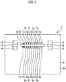
- Fig. 3 is a bottom view of a printed wiring board included in the printed circuit board.
- Fig. 4 is a front view of a printed wiring board included in the printed circuit board.
- Fig. 5 is a back view of the printed wiring board included in the printed circuit board.
- Fig. 6 is a diagram illustrating a cross-section taken along line A-A in Fig. 2 in a state where a coating film of the printed circuit board is not provided.
- Fig. 7 is a diagram illustrating the cross-section taken along the line A-A in Fig. 2 in a state where the coating film of the printed circuit board is provided.
- Fig. 8 to Fig. 11 are main part enlarged views each illustrating an example of the printed circuit board.
- Fig. 12 is a diagram illustrating the cross-section taken along the line A-A in Fig. 2 in a state after a coating film of a printed circuit board (modification) is formed.
- Fig. 13 and Fig. 14 are main part enlarged views each illustrating a modification of the printed circuit board.
- an x-axis, a y-axis, and a z-axis are set as illustrated in Fig. 1 and Fig. 2 .
- the x-axis, the y-axis, and the z-axis are orthogonal to one another.
- a printed circuit board 1 according to the present embodiment includes, for example, a printed wiring board 2, an electronic component 3, a printed wiring board 4, and an electronic component 5.
- the electronic component 3 is provided on the printed wiring board 2.
- the electronic component 5 is provided on the printed wiring board 4.
- the printed wiring board 2 is larger than the printed wiring board 4.
- the printed wiring board 4 is provided to be orthogonal to the printed wiring board 2.
- Fig. 3 is a diagram illustrating an example of the printed wiring board 2.
- the printed wiring board 2 includes, for example, an insulating substrate 6, a plurality of electrodes 7, a pad 8, a plurality of electrodes 9, a pad 10, and lands 11 to 14.
- the insulating substrate 6 has a plate shape with a constant thickness.
- the insulating substrate 6 includes a surface 6a and a surface 6b.
- the electronic component 3 is disposed on the surface 6a.
- the surface 6b is a surface directed to a direction opposite to a direction of the surface 6a.
- the x-axis is parallel to the surface 6a and the surface 6b.
- the y-axis is parallel to the surface 6a and the surface 6b.
- the z-axis is orthogonal to the surface 6a and the surface 6b.
- a mounting hole 15, a mounting hole 16, and a mounting hole 17 are provided in the insulating substrate 6.
- the mounting hole 15, the mounting hole 16, and the mounting hole 17 are holes to mount the printed wiring board 4 on the printed wiring board 2.
- the mounting hole 15, the mounting hole 16, and the mounting hole 17 penetrate through the insulating substrate 6 from the surface 6a to the surface 6b.
- the mounting hole 15 is a long hole in which a width in the y-axis direction is larger than a width in the x-axis direction.
- the mounting hole 16 is a long hole in which a width in the y-axis direction is larger than a width in the x-axis direction.
- the mounting hole 17 is a long hole in which a width in the y-axis direction is larger than a width in the x-axis direction.
- the mounting hole 15, the mounting hole 16, and the mounting hole 17 are arranged in a straight line in the y-axis direction.
- the mounting hole 15 is provided between the mounting hole 16 and the mounting hole 17.
- the printed wiring board 2 includes nine electrodes 7
- the number of electrodes 7 included in the printed wiring board 2 is not limited to nine.
- the electrodes 7 are denoted by reference numerals 7a to 7i to individually specify the electrodes 7.
- the electrodes 7a to 7i are provided on the surface 6b of the insulating substrate 6.
- the electrodes 7a to 7i configure a part of a printed circuit provided on the insulating substrate 6.
- the electrodes 7a to 7i are arranged in a straight line in the y-axis direction.
- the electrodes 7a to 7i are arranged at an edge of the mounting hole 15.
- the electrode 7a is disposed at an end among the electrodes 7a to 7i arranged in a line.
- the electrode 7b is adjacent to the electrode 7a.
- the electrode 7c is adjacent to the first electrode 7b.
- the electrode 7h is adjacent to the electrode 7g.
- the electrode 7i is adjacent to the electrode 7h.
- the electrode 7i is disposed at an end among the electrodes 7a and 7i arranged in a line.
- the pad 8 is provided on the surface 6b of the insulating substrate 6.
- the pad 8 may not configure a part of the printed circuit provided on the insulating substrate 6.
- the pad 8 may not be electrically connected to the electrodes 7a to 7i.
- the electrodes 7a to 7i and the pad 8 are arranged in a line in the y-axis direction.
- the pad 8 is adjacent to the electrode 7i.
- the electrode 7i is disposed between the electrode 7h and the pad 8.
- the pad 8 includes, for example, a solder pool portion, a plurality of adjacent portions, and a termination portion.
- the adjacent portions linearly extend from the solder pool portion toward the electrode 7i.
- the adjacent portions are disposed between the electrode 7i and the solder pool portion.
- the termination portion extends from the solder pool portion in a direction opposite to the extending direction of the adjacent portions. For example, a width of the termination portion in the x-axis direction is gradually reduced as it goes away from the electrode 7i.
- the printed wiring board 2 includes nine electrodes 9 is described.
- the number of electrodes 9 included in the printed wiring board 2 is not limited to nine.
- the electrodes 9 are denoted by reference numerals 9a to 9i to individually specify the electrodes 9.
- the electrodes 9a to 9i are provided on the surface 6b of the insulating substrate 6.
- the electrodes 9a to 9i configure a part of the printed circuit provided on the insulating substrate 6.
- the electrodes 9a to 9i are arranged in a straight line in the y-axis direction.
- the electrodes 9a to 9i are arranged at an edge of the mounting hole 15.
- the electrodes 9a to 9i are arranged to respectively face the electrodes 7a to 7i with the mounting hole 15 in between.
- the electrode 9a is disposed at an end among the electrodes 9a to 9i arranged in a line.
- the electrode 9a is disposed to face the electrode 7a with the mounting hole 15 in between.
- the electrode 9b is adjacent to the electrode 9a.
- the electrode 9b is disposed to face the electrode 7b with the mounting hole 15 in between.
- the electrode 9h is adjacent to the electrode 9g.
- the electrode 9h is disposed to face the electrode 7h with the mounting hole 15 in between.
- the electrode 9i is adjacent to the electrode 9h.
- the electrode 9i is disposed to face the electrode 7i with the mounting hole 15 in between.
- the electrode 9i is disposed at an end among the electrodes 9a to 9i arranged in a line.
- the pad 10 is provided on the surface 6b of the insulating substrate 6.
- the pad 10 may not configure a part of the printed circuit provided on the insulating substrate 6.
- the pad 10 may not be electrically connected to the electrodes 9a to 9i.
- the electrodes 9a to 9i and the pad 10 are arranged in a line in the y-axis direction.
- the pad 10 is adjacent to the electrode 9i.
- the electrode 9i is disposed between the electrode 9h and the pad 10.
- the electrodes 9 and the pad 10 are arranged in a manner similar to the arrangement of the electrodes 7 and the pad 8.
- the pad 10 has a shape similar to the shape of the pad 8.
- the pad 10 includes, for example, a solder pool portion, a plurality of adjacent portions, and a termination portion.
- the adjacent portions linearly extend from the solder pool portion toward the electrode 9i.
- the adjacent portions are disposed between the electrode 9i and the solder pool portion.
- the termination portion extends from the solder pool portion in a direction opposite to the extending direction of the adjacent portions. For example, a width of the termination portion in the x-axis direction is gradually reduced as it goes away from the electrode 9i.
- the lands 11 to 14 are provided on the surface 6b of the insulating substrate 6.
- the lands 11 to 14 may not configure a part of the printed circuit provided on the insulating substrate 6.
- the land 11 and the land 12 are disposed at an edge of the mounting hole 16.
- the land 12 is disposed to sandwich the mounting hole 16 together with the land 11.
- the land 13 and the land 14 are disposed at an edge of the mounting hole 17.
- the land 14 is disposed to sandwich the mounting hole 17 together with the land 13.
- the land 11 and the land 13 are disposed so as to be partially aligned with the electrodes 7a to 7i and the pad 8 in a straight line.
- the land 12 and the land 14 are disposed so as to be partially aligned with the electrodes 9a to 9i and the pad 10 in a straight line.
- Fig. 4 and Fig. 5 are diagrams illustrating an example of the printed wiring board 4.
- the printed wiring board 4 includes, for example, an insulating substrate 18, a plurality of electrodes 19, a pad 20, a land 21, and a land 22.
- the insulating substrate 18 has a plate shape with a constant thickness.
- the insulating substrate 18 includes a surface 18a and a surface 18b.
- Fig. 4 is a diagram illustrating the printed wiring board 4 as viewed from the surface 18a side of the insulating substrate 18.
- the electronic component 5 is disposed on, for example, the front surface 18a.
- the surface 18b is a surface directed to a direction opposite to a direction of the surface 18a.
- the y-axis is parallel to the surface 18a and the surface 18b.
- the z-axis is parallel to the surface 18a and the surface 18b.
- the x-axis is orthogonal to the surface 18a and the surface 18b.
- the insulating substrate 18 includes, for example, a connection portion 23a, a connection portion 23b, and a connection portion 23c.
- the connection portion 23a, the connection portion 23b, and the connection portion 23c are provided on the insulating substrate 18 by, for example, forming a notch 18c and a notch 18d.
- connection portion 23a penetrates through the mounting hole 15 from the surface 6a side, and protrudes from the surface 6b of the insulating substrate 6.
- connection portion 23b penetrates through the mounting hole 16 from the surface 6a side, and protrudes from the surface 6b of the insulating substrate 6.
- connection portion 23c penetrates through the mounting hole 17 from the surface 6a side, and protrudes from the surface 6b of the insulating substrate 6.
- the printed wiring board 4 includes nine electrodes 19 is described.
- the number of electrodes 19 included in the printed wiring board 4 is not limited to nine.
- the electrodes 19 are denoted by reference numerals 19a to 19i to individually specify the electrodes 19.
- the electrodes 19a to 19i are provided on the surface 18a of the insulating substrate 18. More specifically, the electrodes 19a to 19i are provided on the surface 18a of the connection portion 23a.
- the electrodes 19a to 19i configure a part of a printed circuit provided on the insulating substrate 18.
- the electrodes 19a to 19i are arranged in a straight line in the y-axis direction.
- the electrodes 19a to 19i are arranged at an edge of the insulating substrate 18. More specifically, the electrodes 19a to 19i are arranged in the connection portion 23a.
- the electrode 19a is disposed at an end among the electrodes 19a to 19i arranged in a line.
- the electrode 19b is adjacent to the electrode 19a.
- the electrode 19c is adjacent to the electrode 19b.
- the electrode 19h is adjacent to the electrode 19g.
- the electrode 19i is adjacent to the electrode 19h.
- the electrode 19i is disposed at an end among the electrodes 19a to 19i arranged in a line.
- the pad 20 is provided on the surface 18a of the insulating substrate 18. More specifically, the pad 20 is provided on the surface 18a of the connection portion 23a.
- the pad 20 may not configure a part of the printed circuit provided on the insulating substrate 18. For example, the pad 20 may not be electrically connected to the electrodes 19a to 19i.
- the electrodes 19a to 19i and the pad 20 are arranged in a line in the y-axis direction.
- the pad 20 is adjacent to the electrode 19i.
- the electrode 19i is disposed between the electrode 19h and the pad 20.
- the electrodes 19 and the pad 20 are arranged in a manner similar to the arrangement of the electrodes 7 and the pad 8.
- the pad 20 has a shape similar to the shape of the pad 8.
- the pad 20 includes, for example, a solder pool portion, a plurality of adjacent portions, and a termination portion.
- the adjacent portions each include a portion adjacent to the electrode 19i.
- the adjacent portions linearly extend from the solder pool portion toward the electrode 19i.
- the adjacent portions are disposed between the electrode 19i and the solder pool portion. For example, three adjacent portions extend from the solder pool portion toward the electrode 19i.
- the termination portion extends from the solder pool portion in a direction opposite to the extending direction of the adjacent portions.
- the solder pool portion is disposed between the adjacent portions and the termination portion.
- the termination portion has a triangular shape. A width of the termination portion in the z-axis direction is gradually reduced as it goes away from the electrode 19i.
- the land 21 and the land 22 are provided on the surface 18a of the insulating substrate 18. More specifically, the land 21 is provided on the surface 18a of the connection portion 23b. The land 22 is provided on the surface 18a of the connection portion 23c. The land 21 and the land 22 may not configure a part of the printed circuit provided on the insulating substrate 18.
- the land 21 is disposed to sandwich the notch 18c together with the electrode 19a.
- the land 21 is disposed so as to be partially aligned with the electrodes 19a to 19i and the pad 20 in a straight line.
- the land 22 is disposed to sandwich the notch 18d together with the pad 20.
- the land 22 is disposed so as to be partially aligned with the electrodes 19a to 19i and the pad 20 in a straight line.
- Fig. 5 is a diagram illustrating the printed wiring board 4 as viewed from the surface 18b side as a rear surface of the surface 18a.
- a configuration on the surface 18b side is similar to the configuration on the surface 18a side.
- the printed wiring board 4 includes, for example, a plurality of electrodes 25, a pad 26, a land 27, and a land 28.
- the printed wiring board 4 includes nine electrodes 25.
- the number of electrodes 25 included in the printed wiring board 4 is not limited to nine.
- the electrodes 25 are denoted by reference numerals 25a to 25i to individually specify the electrodes 25.
- the electrodes 25a to 25i are provided on the surface 18b of the insulating substrate 18. More specifically, the electrodes 25a to 25i are provided on the surface 18b of the connection portion 23a.
- the electrodes 25a to 25i configure a part of the printed circuit provided on the insulating substrate 18.
- the electrodes 25a to 25i are arranged in a straight line in the y-axis direction.
- the electrodes 25a to 25i are arranged at an edge of the insulating substrate 18. More specifically, the electrodes 25a to 25i are arranged in the connection portion 23a.
- the electrode 25a is disposed at an end among the electrodes 25a to 25i arranged in a line.
- the electrode 25b is adjacent to the electrode 25a.
- the electrode 25h is adjacent to the electrode 25g.
- the electrode 25i is adjacent to the electrode 25h.
- the electrode 25i is disposed at an end among the electrodes 25a to 25i arranged in a line.
- the pad 26 is provided on the surface 18b of the insulating substrate 18. More specifically, the pad 26 is provided on the surface 18b of the connection portion 23a.
- the pad 26 may not configure a part of the printed circuit provided on the insulating substrate 18. For example, the pad 26 may not be electrically connected to the electrodes 25a to 25i.
- the electrodes 25a to 25i and the pad 26 are arranged in a line in the y-axis direction.
- the pad 26 is adjacent to the electrode 25i.
- the electrode 25i is disposed between the electrode 25h of the pad 26.
- the electrodes 25 and the pad 26 are arranged in a manner similar to the arrangement of the electrodes 7 and the pad 8.
- the pad 26 has a shape similar to the shape of the pad 8.
- the pad 26 includes, for example, a solder pool portion, a plurality of adjacent portions, and a termination portion.
- the adjacent portions each include a portion adjacent to the electrode 25i.
- the adjacent portions linearly extend from the solder pool portion toward the electrode 25i.
- the adjacent portions are disposed between the electrode 25i and the solder pool portion. For example, three adjacent portions extend from the solder pool portion toward the electrode 25i.
- the termination portion extends from the solder pool portion in a direction opposite to the extending direction of the adjacent portions.
- the solder pool portion is disposed between the adjacent portions and the termination portion.
- the termination portion has a triangular shape. A width of the termination portion in the z-axis direction is gradually reduced as it goes away from the electrode 25i.
- the land 27 and the land 28 are provided on the surface 18b of the insulating substrate 18. More specifically, the land 27 is provided on the surface 18b of the connection portion 23b. The land 28 is provided on the surface 18b of the connection portion 23c. The land 27 and the land 28 may not configure a part of the printed circuit provided on the insulating substrate 18.
- the land 27 is disposed to sandwich the notch 18c together with the electrode 25a.
- the land 27 is disposed so as to be partially aligned with the electrodes 25a to 25i and the pad 26 in a straight line.
- the land 28 is disposed to sandwich the notch 18d together with the pad 26.
- the land 28 is disposed so as to be partially aligned with the electrodes 25a to 25i and the pad 26 in a straight line.
- the printed circuit board 1 is configured in the following manner by the printed wiring board 2 and the printed wiring board 4 having the above-described configurations.
- the printed wiring board 4 is disposed to be orthogonal to the printed wiring board 2.
- the connection portion 23a is inserted into the mounting hole 15 from the surface 6a side, and is protruded from the surface 6b of the insulating substrate 6.
- the connection portion 23b is inserted into the mounting hole 16, and is protruded from the surface 6b of the insulating substrate 6.
- the connection portion 23c is inserted into the mounting hole 17, and is protruded from the surface 6b of the insulating substrate 6.
- Fig. 6 is a diagram illustrating a cross-section taken along line A-A in Fig. 2 .
- the electrode 7a is provided on the surface 6b of the insulating substrate 6.
- the electrode 19a is disposed to be adjacent to the electrode 7a provided on the insulating substrate 6.
- solder 24 is provided between the electrode 19a and the electrode 7a. The electrode 19a is joined to the electrode 7a by the solder 24.
- the electrode 19b is disposed to be adjacent to the electrode 7b.
- a cross-section including the electrode 19b and the electrode 7b is similar to the cross-section illustrated in Fig. 6 .
- the solder 24 is provided between the electrode 19b and the electrode 7b.
- the electrode 19b is joined to the electrode 7b by the solder 24. Note that the electrode 19b and the electrode 19a are not connected by the solder 24. Further, the electrode 7b and the electrode 7a are not connected by the solder 24.
- the other electrodes 19c to 19i are respectively joined to the electrodes 7c to 7i by the solder in a similar manner.
- the land 21 of the insulating substrate 18 is disposed to be adjacent to the land 11 of the insulating substrate 6.
- a cross-section including the land 21 and the land 11 is similar to the cross-section illustrated in Fig. 6 .
- the solder 24 is provided between the land 21 and the land 11.
- the land 21 is fixed to the land 11 by the solder 24.
- the land 22 of the insulating substrate 18 is disposed to be adjacent to the land 13 of the insulating substrate 6.
- a cross-section including the land 22 and the land 13 is similar to the cross-section illustrated in Fig. 6 .
- the solder 24 is provided between the land 22 and the land 13.
- the land 22 is fixed to the land 13 by the solder 24.
- the electrodes 25a to 25i of the insulating substrate 18 are disposed to be respectively adjacent to the electrodes 9a to 9i provided on the insulating substrate 6. More specifically, for example, the electrode 25a is disposed to be adjacent to the electrode 9a provided on the insulating substrate 6. As illustrated in Fig. 6 , solder 29 is provided between the electrode 25a and the electrode 9a. The electrode 25a is joined to the electrode 9a by the solder 29. As illustrated in Fig. 6 , the electrode 9a is provided on the surface 6b of the insulating substrate 6.
- the electrode 25b is disposed to be adjacent to the electrode 9b.
- a cross-section including the electrode 25b and the electrode 9b is similar to the cross-section illustrated in Fig. 6 .
- the solder 29 is provided between the electrode 25b and the electrode 9b.
- the electrode 25b is joined to the electrode 9b by the solder 29. Note that the electrode 25b and the electrode 25a are not connected by the solder 29.
- the electrode 9b and the electrode 9a are not connected by the solder 29.
- the other electrodes 25c to 25i are respectively joined to the electrodes 9c to 9i by the solder in a similar manner.
- the land 27 of the insulating substrate 18 is disposed to be adjacent to the land 12 of the insulating substrate 6.
- a cross-section including the land 27 and the land 12 is similar to the cross-section illustrated in Fig. 6 .
- the solder 29 is provided between the land 27 and the land 12.
- the land 27 is fixed to the land 12 by the solder 29.
- the land 28 of the insulating substrate 18 is disposed to be adjacent to the land 14 of the insulating substrate 6.
- a cross-section including the land 28 and the land 14 is similar to the cross-section illustrated in Fig. 6 .
- the solder 29 is provided between the land 28 and the land 14.
- the land 28 is fixed to the land 14 by the solder 29.
- the insulating substrate 6 is an example of a first insulating substrate.
- the insulating substrate 6 as the first insulating substrate includes the mounting hole 15.
- the second direction is orthogonal to the first direction.
- the mounting hole 15 is a long hole in which a width in the second direction is larger than a width in the first direction.
- the surface 6a of the insulating substrate 6 is a first surface of the first insulating substrate.
- the surface 6b of the insulating substrate 6 is a second surface of the first insulating substrate.
- the insulating substrate 18 is an example of a second insulating substrate.
- the insulating substrate 18 as the second insulating substrate includes the connection portion 23a that penetrates through the mounting hole 15 from the surface 6a as the first surface and protrudes from the surface 6b as the second surface.
- the electrodes 7 and the electrodes 9 of the insulating substrate 6 are examples of a first electrode provided on the surface 6b as the second surface described above. Further, the electrodes 7 and the electrodes 9 as the first electrodes are arranged at the edge of the mounting hole 15 along the x-axis direction, namely, along the second direction.
- the electrodes 19 and the electrodes 25 of the insulating substrate 18 are examples of a second electrode provided in the connection portion 23a.
- the electrodes 19 and the electrodes 25 as the second electrodes are respectively joined to the first electrodes, namely, the electrodes 7 and the electrodes 9 by the solder 29.
- the surface 6a and the surface 6b of the insulating substrate 6 are covered with a resist 30. However, a portion of each of the electrodes including the electrodes 7 and the electrodes 9 is not covered with the resist 30. Likewise, the surface 18a and the surface 18b of the insulating substrate 18 are covered with the resist 30 except for a portion of each of the electrodes including the electrodes 19 and the electrodes 25. Accordingly, as illustrated in Fig. 6 , the resist 30 is present on a front end side of each of the electrodes 19 and the electrodes 25 in the connection portion 23a.
- a coating film 31 is provided in the connection portion 23a.
- the coating film 31 is provided by, for example, silk printing.
- the coating film 31 is applied and provided on a surface of one or both of the second electrodes (electrodes 19 and electrodes 25) and the resist 30 in the connection portion 23a.
- the coating film 31 is provided at least on the front end side of the connection portion 23a relative to the portions where the second electrodes (electrodes 19 and electrodes 25) are joined to the first electrodes (electrodes 7 and electrodes 9) by the solder.
- connection portion 23a is inserted into the mounting hole 15 from the surface 6a side, and is protruded from the surface 6b of the insulating substrate 6.
- connection portion 23b is inserted into the mounting hole 16 from the surface 6a side, and is protruded from the surface 6b of the insulating substrate 6.
- connection portion 23c is inserted into the mounting hole 17 from the surface 6a side, and is protruded from the surface 6b of the insulating substrate 6.
- the surface 6b is directed downward, and the printed wiring board 2 is fixed to a conveyance device of a flow soldering apparatus.
- the printed wiring board 4 is disposed in a state standing on the printed wiring board 2 such that the connection portions 23a to 23c protrude downward from the printed wiring board 2.
- molten solder is jetted upward from a nozzle.
- the printed wiring board 2 and the printed wiring board 4 supported by the printed wiring board 2 are conveyed by the conveyance device, and pass across above the nozzle.
- a bottom surface of the printed wiring board 2 is immersed in the molten solder jetted from the nozzle.
- a portion of the printed wiring board 4 protruding from the bottom surface of the printed wiring board 2 is immersed in the molten solder jetted from the nozzle.
- the printed wiring board 2 is disposed such that the electrode 7a is immersed in the molten solder from the nozzle before the electrode 7i.
- the printed wiring board 2 is conveyed by the conveyance device in a -y-direction. Therefore, the electrode 7i is immersed in the molten solder next to the electrode 7h, and the pad 8 is immersed in the molten solder after the electrode 7i.
- the printed wiring board 4 is disposed such that the electrode 19a is immersed in the molten solder from the nozzle before the electrode 19i. Therefore, the electrode 19i is immersed in the molten solder next to the electrode 19h, and the pad 20 is immersed in the molten solder next to the electrode 19i.
- the solder 24 is provided between the electrode 7a and the electrode 19a.
- the solder 24 is provided between the electrode 7h and the electrode 19h.
- the solder 24 is provided between the electrode 7i and the electrode 19i.
- the electrodes 7a to 7i are arranged in a line in the conveyance direction by the conveyance device. Therefore, the electrodes 7a to 7i are immersed in the molten solder from the nozzle in order from the electrode 7a.
- the pad 8 is immersed in the molten solder from the nozzle next to the electrode 7i.
- the electrodes 7a to 7i are separated from the molten solder from the nozzle in a similar order. In other words, the electrodes 7a to 7i are separated from the molten solder from the nozzle in order from the electrode 7a.
- the pad 8 is separated from the molten solder from the nozzle next to the electrode 7i.
- the pad 8 is not provided next to the electrode 7i, the solder more than necessary remains in the electrode 7i when the molten solder is separated from the electrode 7i. As a result, what is called a bridge occurs between the electrode 7h and the electrode 7i. In other words, the electrode 7h and the electrode 7i are connected by the solder.
- the pad 8 is provided next to the electrode 7i, it is possible to suppress the solder remaining on the electrode 7i to a necessary amount and to guide the excess solder to the pad 8. This makes it possible to prevent occurrence of the bridge between the electrode 7h and the electrode 7i.
- the molten solder is jetted upward to the electrodes 19 and the electrodes 25 that are the second electrodes of the connection portion 23a protruding downward from the printed wiring board 2. Therefore, when the printed circuit board 1 is separated from the solder jet, the solder for the second electrodes is easily taken by a solder bath side due to influence of gravity and surface tension of the solder.
- the coating film 31 is provided on the front end side of the connection portion 23a relative to the portions where the second electrodes (electrodes 19 and electrodes 25) are joined to the first electrodes (electrodes 7 and electrodes 9) by the solder. Further, the part on the front end side of the connection portion 23a relative to the soldered portions of the second electrodes (electrodes 19 and electrodes 25) is made thick by the coating film 31.
- solder thickness for example, a portion illustrated by arrow in Fig. 7
- shortening of a lifetime due to thermal fatigue at the soldered portions can be suppressed.
- a print pattern of the coating film 31 in the printed circuit board 1 according to the present embodiment is described with reference to Fig. 8 to Fig. 11 .
- the plurality of second electrodes (electrodes 19 and electrodes 25) are arranged in a line in the y-axis direction.
- Fig. 8 and Fig. 9 each illustrate a print pattern example in a case where the coating film 31 is provided for each of the second electrodes.
- the coating film 31 is provided between each of the second electrodes (electrodes 19 and electrodes 25) and the front end of the connection portion 23a.
- the coating films 31 are provided on the surface of the resist 30 of the connection portion 23a. According to such a configuration example, in the flow soldering, it is possible to reduce the amount of solder taken by the solder bath from each of the second electrodes (electrodes 19 and electrodes 25) by the corresponding coating film 31.
- the coating film 31 is disposed in an arc shape at a front end part of each of the second electrodes (electrodes 19 and electrodes 25).
- Each of the coating films 31 is projected toward the front end of the connection portion 23a, and is recessed toward the corresponding second electrode.
- the coating films 31 are provided on the surfaces of both of the second electrodes (electrodes 19 and electrodes 25) and the resist 30 in the connection portion 23a. According to such a configuration example, in the flow soldering, a larger amount of solder can be retained in the inside of the recessed part of each of the arc-shaped coating films 31. This makes it possible to further increase the amount of molten solder adhering to the first electrodes and the second electrodes.
- Fig. 10 and Fig. 11 each illustrate a print pattern example in a case where at least a part of the coating film 31 is linearly provided along the arrangement direction of the second electrodes, namely, along the y-axis direction. More specifically, as illustrated in Fig. 10 , the coating film 31 is linearly provided between the second electrodes (electrodes 19 and electrodes 25) and the front end of the connection portion 23a. Such a configuration also makes it possible to reduce the amount of solder taken by the solder bath from the second electrodes (electrodes 19 and electrodes 25) in the flow soldering, by the linear coating film 31.
- the coating film 31 may be extended from the linear portion to a portion between the second electrodes (electrodes 19 and electrode 25). This makes it possible to prevent occurrence of a bridge between the second electrodes (electrodes 19 and electrodes 25).
- the resist 30 is provided on the front end side of each of the electrodes 19 and the electrodes 25 in the connection portion 23a.
- the electrodes 19 and the electrodes 25 each reach the front end of the connection portion 23a as illustrated in Fig. 12 . Therefore, the coating film 31 is basically applied and provided on the surfaces of the respective second electrodes (electrodes 19 and electrodes 25) of the connection portion 23a.
- an end surface at the front end of the connection portion 23a is coated with the coating film 31.
- the coating film 31 can be formed over both of the surface 18a and the surface 18b of the insulating substrate 18 at a time by, for example, immersing the front end of the connection portion 23a in a paint bath before the process of the flow soldering.
- Fig. 13 illustrates a configuration example in which the coating film 31 is linearly provided along the arrangement direction of the second electrodes, namely, along the y-axis direction over the plurality of second electrodes (electrodes 19 and electrodes 25).
- Such a configuration makes it possible to reduce the amount of solder taken by the solder bath from the second electrodes (electrodes 19 and electrodes 25) in the flow soldering, by the linear coating film 31.
- Fig. 14 illustrates a case where arc-shaped portions 31a are provided in the linear coating film 31 in the configuration example of Fig. 13 .
- the arc-shaped portions 31a are provided to correspond to the respective second electrodes (electrodes 19 and electrodes 25).
- Each of the arc-shaped portions 31a is projected toward the front end of the connection portion 23a, and is recessed toward the corresponding second electrode.
- a larger amount of solder can be retained in the inside of the recessed part of each of the arc-shaped portions 31a of the coating film 31. This makes it possible to further increase the amount of molten solder adhering to the first electrodes and the second electrodes.
- the present invention is usable in the printed circuit board including the plurality of insulating substrates, in particular, the printed circuit board that includes the first insulating substrate provided with the mounting holes, and the second insulating substrate penetrating through the mounting holes of the first insulating substrate and in which the electrodes of the first insulating substrate and the electrodes of the second insulating substrate are joined by the flow soldering.
Landscapes
- Engineering & Computer Science (AREA)
- Microelectronics & Electronic Packaging (AREA)
- Manufacturing & Machinery (AREA)
- Electric Connection Of Electric Components To Printed Circuits (AREA)
- Non-Metallic Protective Coatings For Printed Circuits (AREA)
- Combinations Of Printed Boards (AREA)
Abstract
Description
- The present invention relates to a printed circuit board including a plurality of insulating substrates.
- PTL 1 discloses a printed circuit board. The printed circuit board disclosed in PTL 1 includes a mother board and an auxiliary board. The auxiliary board is inserted into a slit provided in the mother board. A terminal pad provided on the mother board and a terminal pad provided on the auxiliary board are connected by solder.
- [PTL 1]
JP 4314809 B2 - The terminal pad provided on the mother board and the terminal pad provided on the auxiliary board are joined by, for example, flow soldering. More specifically, the mother board and the auxiliary board are conveyed by a conveyance device in a combined state, and are immersed in molten solder that is jetted upward. In a case of the printed circuit board disclosed in PTL 1, when the printed circuit board is separated from the solder jet in the flow soldering, the solder joining the terminal pad provided on the mother board and the terminal pad provided on the auxiliary board is easily taken by a solder bath side due to influence of gravity and surface tension of the solder.
- The present invention is made to solve such issues. An object of the present invention is to provide a printed circuit board in which solder joining electrodes adjacent to each other is prevented from being taken by a solder bath side when the printed circuit board is separated from a solder jet in flow soldering, and an amount of molten solder adhering over the electrodes adjacent to each other is increased.
- A printed circuit board according to the present invention includes: a first insulating substrate having a mounting hole therein, the mounting hole penetrating through the first insulating substrate from a first surface to a second surface; a second insulating substrate including a connection portion, the connection portion penetrating through the mounting hole from the first surface side and protrudes from the second surface; a first electrode provided on the second surface and disposed at an edge of the mounting hole; and a second electrode provided on the connection portion, the first electrode and the second electrode being joined by solder, and the printed circuit board further including a coating film that is disposed at least on a front end side of the connection portion than a portion where the second electrode is joined to the first electrode by the solder.
- According to the printed circuit board of the present invention, when the printed circuit board is separated from the solder jet in the flow soldering, it is possible to prevent the solder joining the electrodes adjacent to each other from being taken by the solder bath side, and to increase the amount of molten solder adhering over the electrodes adjacent to each other.
-
-
Fig. 1 is a perspective views of a printed circuit board according to Embodiment 1 of the present invention. -
Fig. 2 is a perspective views of a printed circuit board according to Embodiment 1 of the present invention. -
Fig. 3 is a bottom view of a printed wiring board included in the printed circuit board according to Embodiment 1 of the present invention. -
Fig. 4 is a front view of a printed wiring board included in the printed circuit board according to Embodiment 1 of the present invention. -
Fig. 5 is a back view of the printed wiring board included in the printed circuit board according to Embodiment 1 of the present invention. -
Fig. 6 is a diagram illustrating a cross-section taken along line A-A inFig. 2 in a state where a coating film of the printed circuit board according to Embodiment 1 of the present invention is not provided. -
Fig. 7 is a diagram illustrating the cross-section taken along the line A-A inFig. 2 in a state where the coating film of the printed circuit board according to Embodiment 1 of the present invention is provided. -
Fig. 8 is a main part enlarged view illustrating an example of the printed circuit board according to Embodiment 1 of the present invention. -
Fig. 9 is a main part enlarged view illustrating an example of the printed circuit board according to Embodiment 1 of the present invention. -
Fig. 10 is a main part enlarged view illustrating an example of the printed circuit board according to Embodiment 1 of the present invention. -
Fig. 11 is a main part enlarged view illustrating an example of the printed circuit board according to Embodiment 1 of the present invention. -
Fig. 12 is a diagram illustrating the cross-section taken along the line A-A inFig. 2 in a state after a coating film of a printed circuit board (modification) according to Embodiment 1 of the present invention is formed. -
Fig. 13 is a main part enlarged view illustrating a modification of the printed circuit board according to Embodiment 1 of the present invention. -
Fig. 14 is a main part enlarged view illustrating a modification of the printed circuit board according to Embodiment 1 of the present invention. - An embodiment of the present invention is described with reference to accompanying drawings. In the drawings, the same or equivalent parts are denoted by the same reference numerals, and repetitive descriptions are appropriately simplified or omitted. Note that the present invention is not limited to the following embodiment, and various modifications can be made without departing from the scope of the present invention.
-
Fig. 1 to Fig. 14 relate to Embodiment 1 of the present invention.Fig. 1 and Fig. 2 are perspective views of a printed circuit board.Fig. 3 is a bottom view of a printed wiring board included in the printed circuit board.Fig. 4 is a front view of a printed wiring board included in the printed circuit board.Fig. 5 is a back view of the printed wiring board included in the printed circuit board.Fig. 6 is a diagram illustrating a cross-section taken along line A-A inFig. 2 in a state where a coating film of the printed circuit board is not provided.Fig. 7 is a diagram illustrating the cross-section taken along the line A-A inFig. 2 in a state where the coating film of the printed circuit board is provided.Fig. 8 to Fig. 11 are main part enlarged views each illustrating an example of the printed circuit board.Fig. 12 is a diagram illustrating the cross-section taken along the line A-A inFig. 2 in a state after a coating film of a printed circuit board (modification) is formed.Fig. 13 andFig. 14 are main part enlarged views each illustrating a modification of the printed circuit board. - To facilitate understanding, an x-axis, a y-axis, and a z-axis are set as illustrated in
Fig. 1 and Fig. 2 . The x-axis, the y-axis, and the z-axis are orthogonal to one another. - A printed circuit board 1 according to the present embodiment includes, for example, a printed
wiring board 2, anelectronic component 3, a printedwiring board 4, and anelectronic component 5. Theelectronic component 3 is provided on the printedwiring board 2. Theelectronic component 5 is provided on the printedwiring board 4. For example, the printedwiring board 2 is larger than the printedwiring board 4. The printedwiring board 4 is provided to be orthogonal to the printedwiring board 2. -
Fig. 3 is a diagram illustrating an example of the printedwiring board 2. The printedwiring board 2 includes, for example, an insulatingsubstrate 6, a plurality ofelectrodes 7, apad 8, a plurality ofelectrodes 9, apad 10, and lands 11 to 14. - For example, the insulating
substrate 6 has a plate shape with a constant thickness. The insulatingsubstrate 6 includes asurface 6a and asurface 6b. Theelectronic component 3 is disposed on thesurface 6a. Thesurface 6b is a surface directed to a direction opposite to a direction of thesurface 6a. The x-axis is parallel to thesurface 6a and thesurface 6b. The y-axis is parallel to thesurface 6a and thesurface 6b. The z-axis is orthogonal to thesurface 6a and thesurface 6b. - A mounting hole 15, a mounting
hole 16, and a mounting hole 17 are provided in the insulatingsubstrate 6. The mounting hole 15, the mountinghole 16, and the mounting hole 17 are holes to mount the printedwiring board 4 on the printedwiring board 2. The mounting hole 15, the mountinghole 16, and the mounting hole 17 penetrate through the insulatingsubstrate 6 from thesurface 6a to thesurface 6b. The mounting hole 15 is a long hole in which a width in the y-axis direction is larger than a width in the x-axis direction. Likewise, the mountinghole 16 is a long hole in which a width in the y-axis direction is larger than a width in the x-axis direction. The mounting hole 17 is a long hole in which a width in the y-axis direction is larger than a width in the x-axis direction. The mounting hole 15, the mountinghole 16, and the mounting hole 17 are arranged in a straight line in the y-axis direction. The mounting hole 15 is provided between the mountinghole 16 and the mounting hole 17. - In the present embodiment, an example in which the printed
wiring board 2 includes nineelectrodes 7 is described. The number ofelectrodes 7 included in the printedwiring board 2 is not limited to nine. In the following description, theelectrodes 7 are denoted byreference numerals 7a to 7i to individually specify theelectrodes 7. Theelectrodes 7a to 7i are provided on thesurface 6b of the insulatingsubstrate 6. Theelectrodes 7a to 7i configure a part of a printed circuit provided on the insulatingsubstrate 6. - The
electrodes 7a to 7i are arranged in a straight line in the y-axis direction. Theelectrodes 7a to 7i are arranged at an edge of the mounting hole 15. For example, theelectrode 7a is disposed at an end among theelectrodes 7a to 7i arranged in a line. Theelectrode 7b is adjacent to theelectrode 7a. The electrode 7c is adjacent to thefirst electrode 7b. Likewise, theelectrode 7h is adjacent to the electrode 7g. Theelectrode 7i is adjacent to theelectrode 7h. Theelectrode 7i is disposed at an end among theelectrodes - The
pad 8 is provided on thesurface 6b of the insulatingsubstrate 6. Thepad 8 may not configure a part of the printed circuit provided on the insulatingsubstrate 6. For example, thepad 8 may not be electrically connected to theelectrodes 7a to 7i. Theelectrodes 7a to 7i and thepad 8 are arranged in a line in the y-axis direction. Thepad 8 is adjacent to theelectrode 7i. Theelectrode 7i is disposed between theelectrode 7h and thepad 8. - The
pad 8 includes, for example, a solder pool portion, a plurality of adjacent portions, and a termination portion. The adjacent portions linearly extend from the solder pool portion toward theelectrode 7i. The adjacent portions are disposed between theelectrode 7i and the solder pool portion. The termination portion extends from the solder pool portion in a direction opposite to the extending direction of the adjacent portions. For example, a width of the termination portion in the x-axis direction is gradually reduced as it goes away from theelectrode 7i. - In the present embodiment, an example in which the printed
wiring board 2 includes nineelectrodes 9 is described. The number ofelectrodes 9 included in the printedwiring board 2 is not limited to nine. In the following description, theelectrodes 9 are denoted byreference numerals 9a to 9i to individually specify theelectrodes 9. Theelectrodes 9a to 9i are provided on thesurface 6b of the insulatingsubstrate 6. Theelectrodes 9a to 9i configure a part of the printed circuit provided on the insulatingsubstrate 6. - The
electrodes 9a to 9i are arranged in a straight line in the y-axis direction. Theelectrodes 9a to 9i are arranged at an edge of the mounting hole 15. Theelectrodes 9a to 9i are arranged to respectively face theelectrodes 7a to 7i with the mounting hole 15 in between. For example, theelectrode 9a is disposed at an end among theelectrodes 9a to 9i arranged in a line. Theelectrode 9a is disposed to face theelectrode 7a with the mounting hole 15 in between. The electrode 9b is adjacent to theelectrode 9a. The electrode 9b is disposed to face theelectrode 7b with the mounting hole 15 in between. Likewise, the electrode 9h is adjacent to theelectrode 9g. The electrode 9h is disposed to face theelectrode 7h with the mounting hole 15 in between. The electrode 9i is adjacent to the electrode 9h. The electrode 9i is disposed to face theelectrode 7i with the mounting hole 15 in between. The electrode 9i is disposed at an end among theelectrodes 9a to 9i arranged in a line. - The
pad 10 is provided on thesurface 6b of the insulatingsubstrate 6. Thepad 10 may not configure a part of the printed circuit provided on the insulatingsubstrate 6. For example, thepad 10 may not be electrically connected to theelectrodes 9a to 9i. Theelectrodes 9a to 9i and thepad 10 are arranged in a line in the y-axis direction. Thepad 10 is adjacent to the electrode 9i. The electrode 9i is disposed between the electrode 9h and thepad 10. - The
electrodes 9 and thepad 10 are arranged in a manner similar to the arrangement of theelectrodes 7 and thepad 8. Thepad 10 has a shape similar to the shape of thepad 8. Thepad 10 includes, for example, a solder pool portion, a plurality of adjacent portions, and a termination portion. The adjacent portions linearly extend from the solder pool portion toward the electrode 9i. The adjacent portions are disposed between the electrode 9i and the solder pool portion. The termination portion extends from the solder pool portion in a direction opposite to the extending direction of the adjacent portions. For example, a width of the termination portion in the x-axis direction is gradually reduced as it goes away from the electrode 9i. - The
lands 11 to 14 are provided on thesurface 6b of the insulatingsubstrate 6. Thelands 11 to 14 may not configure a part of the printed circuit provided on the insulatingsubstrate 6. Theland 11 and theland 12 are disposed at an edge of the mountinghole 16. Theland 12 is disposed to sandwich the mountinghole 16 together with theland 11. Theland 13 and theland 14 are disposed at an edge of the mounting hole 17. Theland 14 is disposed to sandwich the mounting hole 17 together with theland 13. Theland 11 and theland 13 are disposed so as to be partially aligned with theelectrodes 7a to 7i and thepad 8 in a straight line. Theland 12 and theland 14 are disposed so as to be partially aligned with theelectrodes 9a to 9i and thepad 10 in a straight line. -
Fig. 4 and Fig. 5 are diagrams illustrating an example of the printedwiring board 4. As illustrated inFig. 4 , the printedwiring board 4 includes, for example, an insulatingsubstrate 18, a plurality ofelectrodes 19, apad 20, aland 21, and aland 22. - For example, the insulating
substrate 18 has a plate shape with a constant thickness. The insulatingsubstrate 18 includes asurface 18a and asurface 18b.Fig. 4 is a diagram illustrating the printedwiring board 4 as viewed from thesurface 18a side of the insulatingsubstrate 18. Theelectronic component 5 is disposed on, for example, thefront surface 18a. Thesurface 18b is a surface directed to a direction opposite to a direction of thesurface 18a. The y-axis is parallel to thesurface 18a and thesurface 18b. The z-axis is parallel to thesurface 18a and thesurface 18b. The x-axis is orthogonal to thesurface 18a and thesurface 18b. - The insulating
substrate 18 includes, for example, aconnection portion 23a, aconnection portion 23b, and aconnection portion 23c. Theconnection portion 23a, theconnection portion 23b, and theconnection portion 23c are provided on the insulatingsubstrate 18 by, for example, forming anotch 18c and anotch 18d. - The
connection portion 23a penetrates through the mounting hole 15 from thesurface 6a side, and protrudes from thesurface 6b of the insulatingsubstrate 6. Theconnection portion 23b penetrates through the mountinghole 16 from thesurface 6a side, and protrudes from thesurface 6b of the insulatingsubstrate 6. Further, theconnection portion 23c penetrates through the mounting hole 17 from thesurface 6a side, and protrudes from thesurface 6b of the insulatingsubstrate 6. - In the present embodiment, an example in which the printed
wiring board 4 includes nineelectrodes 19 is described. The number ofelectrodes 19 included in the printedwiring board 4 is not limited to nine. In the following description, theelectrodes 19 are denoted byreference numerals 19a to 19i to individually specify theelectrodes 19. Theelectrodes 19a to 19i are provided on thesurface 18a of the insulatingsubstrate 18. More specifically, theelectrodes 19a to 19i are provided on thesurface 18a of theconnection portion 23a. Theelectrodes 19a to 19i configure a part of a printed circuit provided on the insulatingsubstrate 18. - The
electrodes 19a to 19i are arranged in a straight line in the y-axis direction. Theelectrodes 19a to 19i are arranged at an edge of the insulatingsubstrate 18. More specifically, theelectrodes 19a to 19i are arranged in theconnection portion 23a. For example, theelectrode 19a is disposed at an end among theelectrodes 19a to 19i arranged in a line. Theelectrode 19b is adjacent to theelectrode 19a. Theelectrode 19c is adjacent to theelectrode 19b. Theelectrode 19h is adjacent to theelectrode 19g. Theelectrode 19i is adjacent to theelectrode 19h. Theelectrode 19i is disposed at an end among theelectrodes 19a to 19i arranged in a line. - The
pad 20 is provided on thesurface 18a of the insulatingsubstrate 18. More specifically, thepad 20 is provided on thesurface 18a of theconnection portion 23a. Thepad 20 may not configure a part of the printed circuit provided on the insulatingsubstrate 18. For example, thepad 20 may not be electrically connected to theelectrodes 19a to 19i. Theelectrodes 19a to 19i and thepad 20 are arranged in a line in the y-axis direction. Thepad 20 is adjacent to theelectrode 19i. Theelectrode 19i is disposed between theelectrode 19h and thepad 20. - The
electrodes 19 and thepad 20 are arranged in a manner similar to the arrangement of theelectrodes 7 and thepad 8. Thepad 20 has a shape similar to the shape of thepad 8. Thepad 20 includes, for example, a solder pool portion, a plurality of adjacent portions, and a termination portion. The adjacent portions each include a portion adjacent to theelectrode 19i. The adjacent portions linearly extend from the solder pool portion toward theelectrode 19i. The adjacent portions are disposed between theelectrode 19i and the solder pool portion. For example, three adjacent portions extend from the solder pool portion toward theelectrode 19i. - The termination portion extends from the solder pool portion in a direction opposite to the extending direction of the adjacent portions. The solder pool portion is disposed between the adjacent portions and the termination portion. For example, the termination portion has a triangular shape. A width of the termination portion in the z-axis direction is gradually reduced as it goes away from the
electrode 19i. - The
land 21 and theland 22 are provided on thesurface 18a of the insulatingsubstrate 18. More specifically, theland 21 is provided on thesurface 18a of theconnection portion 23b. Theland 22 is provided on thesurface 18a of theconnection portion 23c. Theland 21 and theland 22 may not configure a part of the printed circuit provided on the insulatingsubstrate 18. - The
land 21 is disposed to sandwich thenotch 18c together with theelectrode 19a. Theland 21 is disposed so as to be partially aligned with theelectrodes 19a to 19i and thepad 20 in a straight line. Theland 22 is disposed to sandwich thenotch 18d together with thepad 20. Theland 22 is disposed so as to be partially aligned with theelectrodes 19a to 19i and thepad 20 in a straight line. -
Fig. 5 is a diagram illustrating the printedwiring board 4 as viewed from thesurface 18b side as a rear surface of thesurface 18a. In the printedwiring board 4, a configuration on thesurface 18b side is similar to the configuration on thesurface 18a side. The printedwiring board 4 includes, for example, a plurality ofelectrodes 25, apad 26, aland 27, and aland 28. - In the present embodiment, an example in which the printed
wiring board 4 includes nineelectrodes 25 is described. The number ofelectrodes 25 included in the printedwiring board 4 is not limited to nine. In the following description, theelectrodes 25 are denoted byreference numerals 25a to 25i to individually specify theelectrodes 25. Theelectrodes 25a to 25i are provided on thesurface 18b of the insulatingsubstrate 18. More specifically, theelectrodes 25a to 25i are provided on thesurface 18b of theconnection portion 23a. Theelectrodes 25a to 25i configure a part of the printed circuit provided on the insulatingsubstrate 18. - The
electrodes 25a to 25i are arranged in a straight line in the y-axis direction. Theelectrodes 25a to 25i are arranged at an edge of the insulatingsubstrate 18. More specifically, theelectrodes 25a to 25i are arranged in theconnection portion 23a. For example, theelectrode 25a is disposed at an end among theelectrodes 25a to 25i arranged in a line. Theelectrode 25b is adjacent to theelectrode 25a. Theelectrode 25h is adjacent to theelectrode 25g. Theelectrode 25i is adjacent to theelectrode 25h. Theelectrode 25i is disposed at an end among theelectrodes 25a to 25i arranged in a line. - The
pad 26 is provided on thesurface 18b of the insulatingsubstrate 18. More specifically, thepad 26 is provided on thesurface 18b of theconnection portion 23a. Thepad 26 may not configure a part of the printed circuit provided on the insulatingsubstrate 18. For example, thepad 26 may not be electrically connected to theelectrodes 25a to 25i. Theelectrodes 25a to 25i and thepad 26 are arranged in a line in the y-axis direction. Thepad 26 is adjacent to theelectrode 25i. Theelectrode 25i is disposed between theelectrode 25h of thepad 26. - The
electrodes 25 and thepad 26 are arranged in a manner similar to the arrangement of theelectrodes 7 and thepad 8. Thepad 26 has a shape similar to the shape of thepad 8. Thepad 26 includes, for example, a solder pool portion, a plurality of adjacent portions, and a termination portion. The adjacent portions each include a portion adjacent to theelectrode 25i. The adjacent portions linearly extend from the solder pool portion toward theelectrode 25i. The adjacent portions are disposed between theelectrode 25i and the solder pool portion. For example, three adjacent portions extend from the solder pool portion toward theelectrode 25i. - The termination portion extends from the solder pool portion in a direction opposite to the extending direction of the adjacent portions. The solder pool portion is disposed between the adjacent portions and the termination portion. For example, the termination portion has a triangular shape. A width of the termination portion in the z-axis direction is gradually reduced as it goes away from the
electrode 25i. - The
land 27 and theland 28 are provided on thesurface 18b of the insulatingsubstrate 18. More specifically, theland 27 is provided on thesurface 18b of theconnection portion 23b. Theland 28 is provided on thesurface 18b of theconnection portion 23c. Theland 27 and theland 28 may not configure a part of the printed circuit provided on the insulatingsubstrate 18. - The
land 27 is disposed to sandwich thenotch 18c together with theelectrode 25a. Theland 27 is disposed so as to be partially aligned with theelectrodes 25a to 25i and thepad 26 in a straight line. Theland 28 is disposed to sandwich thenotch 18d together with thepad 26. Theland 28 is disposed so as to be partially aligned with theelectrodes 25a to 25i and thepad 26 in a straight line. - The printed circuit board 1 is configured in the following manner by the printed
wiring board 2 and the printedwiring board 4 having the above-described configurations. First, the printedwiring board 4 is disposed to be orthogonal to the printedwiring board 2. At this time, theconnection portion 23a is inserted into the mounting hole 15 from thesurface 6a side, and is protruded from thesurface 6b of the insulatingsubstrate 6. Theconnection portion 23b is inserted into the mountinghole 16, and is protruded from thesurface 6b of the insulatingsubstrate 6. Theconnection portion 23c is inserted into the mounting hole 17, and is protruded from thesurface 6b of the insulatingsubstrate 6. - In this state, as illustrated in
Fig. 2 , theelectrodes 19a to 19i of the insulatingsubstrate 18 are disposed to be respectively adjacent to theelectrodes 7a to 7i provided on the insulatingsubstrate 6.Fig. 6 is a diagram illustrating a cross-section taken along line A-A inFig. 2 . As illustrated inFig. 6 , theelectrode 7a is provided on thesurface 6b of the insulatingsubstrate 6. Theelectrode 19a is disposed to be adjacent to theelectrode 7a provided on the insulatingsubstrate 6. Further,solder 24 is provided between theelectrode 19a and theelectrode 7a. Theelectrode 19a is joined to theelectrode 7a by thesolder 24. - In addition, the
electrode 19b is disposed to be adjacent to theelectrode 7b. A cross-section including theelectrode 19b and theelectrode 7b is similar to the cross-section illustrated inFig. 6 . Thesolder 24 is provided between theelectrode 19b and theelectrode 7b. Theelectrode 19b is joined to theelectrode 7b by thesolder 24. Note that theelectrode 19b and theelectrode 19a are not connected by thesolder 24. Further, theelectrode 7b and theelectrode 7a are not connected by thesolder 24. - The
other electrodes 19c to 19i are respectively joined to the electrodes 7c to 7i by the solder in a similar manner. - The
land 21 of the insulatingsubstrate 18 is disposed to be adjacent to theland 11 of the insulatingsubstrate 6. A cross-section including theland 21 and theland 11 is similar to the cross-section illustrated inFig. 6 . Thesolder 24 is provided between theland 21 and theland 11. Theland 21 is fixed to theland 11 by thesolder 24. In addition, theland 22 of the insulatingsubstrate 18 is disposed to be adjacent to theland 13 of the insulatingsubstrate 6. A cross-section including theland 22 and theland 13 is similar to the cross-section illustrated inFig. 6 . Thesolder 24 is provided between theland 22 and theland 13. Theland 22 is fixed to theland 13 by thesolder 24. - Further, in this state, the
electrodes 25a to 25i of the insulatingsubstrate 18 are disposed to be respectively adjacent to theelectrodes 9a to 9i provided on the insulatingsubstrate 6. More specifically, for example, theelectrode 25a is disposed to be adjacent to theelectrode 9a provided on the insulatingsubstrate 6. As illustrated inFig. 6 ,solder 29 is provided between theelectrode 25a and theelectrode 9a. Theelectrode 25a is joined to theelectrode 9a by thesolder 29. As illustrated inFig. 6 , theelectrode 9a is provided on thesurface 6b of the insulatingsubstrate 6. - Further, the
electrode 25b is disposed to be adjacent to the electrode 9b. A cross-section including theelectrode 25b and the electrode 9b is similar to the cross-section illustrated inFig. 6 . Thesolder 29 is provided between theelectrode 25b and the electrode 9b. Theelectrode 25b is joined to the electrode 9b by thesolder 29. Note that theelectrode 25b and theelectrode 25a are not connected by thesolder 29. The electrode 9b and theelectrode 9a are not connected by thesolder 29. - The
other electrodes 25c to 25i are respectively joined to theelectrodes 9c to 9i by the solder in a similar manner. - The
land 27 of the insulatingsubstrate 18 is disposed to be adjacent to theland 12 of the insulatingsubstrate 6. A cross-section including theland 27 and theland 12 is similar to the cross-section illustrated inFig. 6 . Thesolder 29 is provided between theland 27 and theland 12. Theland 27 is fixed to theland 12 by thesolder 29. In addition, theland 28 of the insulatingsubstrate 18 is disposed to be adjacent to theland 14 of the insulatingsubstrate 6. A cross-section including theland 28 and theland 14 is similar to the cross-section illustrated inFig. 6 . Thesolder 29 is provided between theland 28 and theland 14. Theland 28 is fixed to theland 14 by thesolder 29. - In the printed circuit board 1 having the above-described configuration according to Embodiment 1, the insulating
substrate 6 is an example of a first insulating substrate. The insulatingsubstrate 6 as the first insulating substrate includes the mounting hole 15. When the y-axis direction is defined as a first direction and the x-axis direction is defined as a second direction, the second direction is orthogonal to the first direction. The mounting hole 15 is a long hole in which a width in the second direction is larger than a width in the first direction. In addition, thesurface 6a of the insulatingsubstrate 6 is a first surface of the first insulating substrate. Thesurface 6b of the insulatingsubstrate 6 is a second surface of the first insulating substrate. - In the printed circuit board 1 according to Embodiment 1, the insulating
substrate 18 is an example of a second insulating substrate. The insulatingsubstrate 18 as the second insulating substrate includes theconnection portion 23a that penetrates through the mounting hole 15 from thesurface 6a as the first surface and protrudes from thesurface 6b as the second surface. Theelectrodes 7 and theelectrodes 9 of the insulatingsubstrate 6 are examples of a first electrode provided on thesurface 6b as the second surface described above. Further, theelectrodes 7 and theelectrodes 9 as the first electrodes are arranged at the edge of the mounting hole 15 along the x-axis direction, namely, along the second direction. - The
electrodes 19 and theelectrodes 25 of the insulatingsubstrate 18 are examples of a second electrode provided in theconnection portion 23a. Theelectrodes 19 and theelectrodes 25 as the second electrodes are respectively joined to the first electrodes, namely, theelectrodes 7 and theelectrodes 9 by thesolder 29. - The
surface 6a and thesurface 6b of the insulatingsubstrate 6 are covered with a resist 30. However, a portion of each of the electrodes including theelectrodes 7 and theelectrodes 9 is not covered with the resist 30. Likewise, thesurface 18a and thesurface 18b of the insulatingsubstrate 18 are covered with the resist 30 except for a portion of each of the electrodes including theelectrodes 19 and theelectrodes 25. Accordingly, as illustrated inFig. 6 , the resist 30 is present on a front end side of each of theelectrodes 19 and theelectrodes 25 in theconnection portion 23a. - Further, as illustrated in
Fig. 7 , acoating film 31 is provided in theconnection portion 23a. Thecoating film 31 is provided by, for example, silk printing. Thecoating film 31 is applied and provided on a surface of one or both of the second electrodes (electrodes 19 and electrodes 25) and the resist 30 in theconnection portion 23a. Thecoating film 31 is provided at least on the front end side of theconnection portion 23a relative to the portions where the second electrodes (electrodes 19 and electrodes 25) are joined to the first electrodes (electrodes 7 and electrodes 9) by the solder. - Next, a method of joining the printed
wiring board 2 illustrated inFig. 3 having the above-described configuration and the printedwiring board 4 illustrated inFig. 4 and Fig. 5 having the above-described configuration, by the solder is described. - First, the printed
wiring board 4 is disposed to be orthogonal to the printedwiring board 2. At this time, theconnection portion 23a is inserted into the mounting hole 15 from thesurface 6a side, and is protruded from thesurface 6b of the insulatingsubstrate 6. Further, theconnection portion 23b is inserted into the mountinghole 16 from thesurface 6a side, and is protruded from thesurface 6b of the insulatingsubstrate 6. Theconnection portion 23c is inserted into the mounting hole 17 from thesurface 6a side, and is protruded from thesurface 6b of the insulatingsubstrate 6. - Next, the
surface 6b is directed downward, and the printedwiring board 2 is fixed to a conveyance device of a flow soldering apparatus. The printedwiring board 4 is disposed in a state standing on the printedwiring board 2 such that theconnection portions 23a to 23c protrude downward from the printedwiring board 2. In the flow soldering apparatus, molten solder is jetted upward from a nozzle. The printedwiring board 2 and the printedwiring board 4 supported by the printedwiring board 2 are conveyed by the conveyance device, and pass across above the nozzle. When the printedwiring board 2 passes above the nozzle, a bottom surface of the printedwiring board 2 is immersed in the molten solder jetted from the nozzle. In addition, a portion of the printedwiring board 4 protruding from the bottom surface of the printedwiring board 2 is immersed in the molten solder jetted from the nozzle. - The printed
wiring board 2 is disposed such that theelectrode 7a is immersed in the molten solder from the nozzle before theelectrode 7i. In the case of the configuration example illustrated inFig. 1 and Fig. 2 , the printedwiring board 2 is conveyed by the conveyance device in a -y-direction. Therefore, theelectrode 7i is immersed in the molten solder next to theelectrode 7h, and thepad 8 is immersed in the molten solder after theelectrode 7i. Further, the printedwiring board 4 is disposed such that theelectrode 19a is immersed in the molten solder from the nozzle before theelectrode 19i. Therefore, theelectrode 19i is immersed in the molten solder next to theelectrode 19h, and thepad 20 is immersed in the molten solder next to theelectrode 19i. - For example, when the
electrode 7a and theelectrode 19a are immersed in the molten solder from the nozzle, thesolder 24 is provided between theelectrode 7a and theelectrode 19a. Likewise, when theelectrode 7h and theelectrode 19h are immersed in the molten solder from the nozzle, thesolder 24 is provided between theelectrode 7h and theelectrode 19h. When theelectrode 7i and theelectrode 19i are immersed in the molten solder from the nozzle, thesolder 24 is provided between theelectrode 7i and theelectrode 19i. - In the configuration example illustrated in the present embodiment, the
electrodes 7a to 7i are arranged in a line in the conveyance direction by the conveyance device. Therefore, theelectrodes 7a to 7i are immersed in the molten solder from the nozzle in order from theelectrode 7a. Thepad 8 is immersed in the molten solder from the nozzle next to theelectrode 7i. Theelectrodes 7a to 7i are separated from the molten solder from the nozzle in a similar order. In other words, theelectrodes 7a to 7i are separated from the molten solder from the nozzle in order from theelectrode 7a. Thepad 8 is separated from the molten solder from the nozzle next to theelectrode 7i. - If the
pad 8 is not provided next to theelectrode 7i, the solder more than necessary remains in theelectrode 7i when the molten solder is separated from theelectrode 7i. As a result, what is called a bridge occurs between theelectrode 7h and theelectrode 7i. In other words, theelectrode 7h and theelectrode 7i are connected by the solder. When thepad 8 is provided next to theelectrode 7i, it is possible to suppress the solder remaining on theelectrode 7i to a necessary amount and to guide the excess solder to thepad 8. This makes it possible to prevent occurrence of the bridge between theelectrode 7h and theelectrode 7i. - Further, the molten solder is jetted upward to the
electrodes 19 and theelectrodes 25 that are the second electrodes of theconnection portion 23a protruding downward from the printedwiring board 2. Therefore, when the printed circuit board 1 is separated from the solder jet, the solder for the second electrodes is easily taken by a solder bath side due to influence of gravity and surface tension of the solder. - In this regard, in the printed circuit board 1 according to the present embodiment, the
coating film 31 is provided on the front end side of theconnection portion 23a relative to the portions where the second electrodes (electrodes 19 and electrodes 25) are joined to the first electrodes (electrodes 7 and electrodes 9) by the solder. Further, the part on the front end side of theconnection portion 23a relative to the soldered portions of the second electrodes (electrodes 19 and electrodes 25) is made thick by thecoating film 31. Accordingly, a larger amount of solder can be retained on the second electrodes (electrode 19 and electrodes 25) on an upper side of thecoating film 31, and it is possible to prevent the solder for the second electrodes (electrodes 19 and electrodes 25) from being taken by the solder bath from the front end side of theconnection portion 23a. This makes it possible to increase the amount of molten solder adhering over the first electrodes (electrodes 7 and electrodes 9) and the second electrodes (electrodes 19 and electrodes 25). In other words, a solder thickness (for example, a portion illustrated by arrow inFig. 7 ) by flow soldering can be stably made thick, and shortening of a lifetime due to thermal fatigue at the soldered portions can be suppressed. - Next, specific examples of a print pattern of the
coating film 31 in the printed circuit board 1 according to the present embodiment are described with reference toFig. 8 to Fig. 11 . As described above, in the configuration example of the present embodiment, the plurality of second electrodes (electrodes 19 and electrodes 25) are arranged in a line in the y-axis direction.Fig. 8 and Fig. 9 each illustrate a print pattern example in a case where thecoating film 31 is provided for each of the second electrodes. - First, in the example illustrated in
Fig. 8 , thecoating film 31 is provided between each of the second electrodes (electrodes 19 and electrodes 25) and the front end of theconnection portion 23a. In this configuration example, the coatingfilms 31 are provided on the surface of the resist 30 of theconnection portion 23a. According to such a configuration example, in the flow soldering, it is possible to reduce the amount of solder taken by the solder bath from each of the second electrodes (electrodes 19 and electrodes 25) by the correspondingcoating film 31. - Next, in the example illustrated in
Fig. 9 , thecoating film 31 is disposed in an arc shape at a front end part of each of the second electrodes (electrodes 19 and electrodes 25). Each of thecoating films 31 is projected toward the front end of theconnection portion 23a, and is recessed toward the corresponding second electrode. In this configuration example, the coatingfilms 31 are provided on the surfaces of both of the second electrodes (electrodes 19 and electrodes 25) and the resist 30 in theconnection portion 23a. According to such a configuration example, in the flow soldering, a larger amount of solder can be retained in the inside of the recessed part of each of the arc-shapedcoating films 31. This makes it possible to further increase the amount of molten solder adhering to the first electrodes and the second electrodes. - In contrast,
Fig. 10 and Fig. 11 each illustrate a print pattern example in a case where at least a part of thecoating film 31 is linearly provided along the arrangement direction of the second electrodes, namely, along the y-axis direction. More specifically, as illustrated inFig. 10 , thecoating film 31 is linearly provided between the second electrodes (electrodes 19 and electrodes 25) and the front end of theconnection portion 23a. Such a configuration also makes it possible to reduce the amount of solder taken by the solder bath from the second electrodes (electrodes 19 and electrodes 25) in the flow soldering, by thelinear coating film 31. - Alternatively, as illustrated in
Fig. 11 , thecoating film 31 may be extended from the linear portion to a portion between the second electrodes (electrodes 19 and electrode 25). This makes it possible to prevent occurrence of a bridge between the second electrodes (electrodes 19 and electrodes 25). - Next, a modification of the printed circuit board 1 according to the present embodiment is described with reference to
Fig. 12 to Fig. 14 . In the configuration examples described above, for example, as illustrated inFig. 6 , the resist 30 is provided on the front end side of each of theelectrodes 19 and theelectrodes 25 in theconnection portion 23a. In contrast, in the modification described below, theelectrodes 19 and theelectrodes 25 each reach the front end of theconnection portion 23a as illustrated inFig. 12 . Therefore, thecoating film 31 is basically applied and provided on the surfaces of the respective second electrodes (electrodes 19 and electrodes 25) of theconnection portion 23a. - In particular, in the configuration example illustrated in
Fig. 12 , an end surface at the front end of theconnection portion 23a is coated with thecoating film 31. As a result, in manufacturing the printed circuit board 1, thecoating film 31 can be formed over both of thesurface 18a and thesurface 18b of the insulatingsubstrate 18 at a time by, for example, immersing the front end of theconnection portion 23a in a paint bath before the process of the flow soldering. - Next, a specific example of the print pattern of the
coating film 31 in the modification of the printed circuit board 1 according to the present embodiment is described.Fig. 13 illustrates a configuration example in which thecoating film 31 is linearly provided along the arrangement direction of the second electrodes, namely, along the y-axis direction over the plurality of second electrodes (electrodes 19 and electrodes 25). Such a configuration makes it possible to reduce the amount of solder taken by the solder bath from the second electrodes (electrodes 19 and electrodes 25) in the flow soldering, by thelinear coating film 31. -
Fig. 14 illustrates a case where arc-shapedportions 31a are provided in thelinear coating film 31 in the configuration example ofFig. 13 . The arc-shapedportions 31a are provided to correspond to the respective second electrodes (electrodes 19 and electrodes 25). Each of the arc-shapedportions 31a is projected toward the front end of theconnection portion 23a, and is recessed toward the corresponding second electrode. According to such a configuration example, in the flow soldering, a larger amount of solder can be retained in the inside of the recessed part of each of the arc-shapedportions 31a of thecoating film 31. This makes it possible to further increase the amount of molten solder adhering to the first electrodes and the second electrodes. - The present invention is usable in the printed circuit board including the plurality of insulating substrates, in particular, the printed circuit board that includes the first insulating substrate provided with the mounting holes, and the second insulating substrate penetrating through the mounting holes of the first insulating substrate and in which the electrodes of the first insulating substrate and the electrodes of the second insulating substrate are joined by the flow soldering.
-
- 1 Printed circuit board
- 2 Printed wiring board
- 3 Electronic component
- 4 Printed wiring board
- 5 Electronic component
- 6 Insulating substrate (First insulating substrate)
- 6a Surface (First surface)
- 6b Surface (Second surface)
- 7 Electrode (First electrode)
- 8 Pad
- 9 Electrode (First electrode)
- 10 Pad
- 11-14 Lands
- 15-17 Mounting holes
- 18 Insulating substrate (Second insulating substrate)
- 18a-b Surfaces
- 18c-d Notches
- 19 Electrode (Second electrode)
- 20 Pad
- 21-22 Lands
- 23a-23c Connection portions
- 24 Solder
- 25 Electrode (Second electrode)
- 26 Pad
- 27-28 Lands
- 29 Solder
- 30 Resist
- 31 Coating film
- 31a Arc-shaped portion
Claims (5)
- A printed circuit board, comprising:a first insulating substrate having a mounting hole therein, the mounting hole penetrating through the first insulating substrate from a first surface to a second surface;a second insulating substrate including a connection portion, the connection portion penetrating through the mounting hole from the first surface side and protrudes from the second surface;a first electrode provided on the second surface and disposed at an edge of the mounting hole; anda second electrode provided on the connection portion,the first electrode and the second electrode being joined by solder, andthe printed circuit board further including a coating film that is disposed at least on a front end side of the connection portion than a portion where the second electrode is joined to the first electrode by the solder.
- The printed circuit board according to claim 1, further comprising a resist provided on a portion not provided with the second electrode in the connection portion, wherein
the coating film is applied and provided on a surface of one or both of the second electrode and the resist in the connection portion. - The printed circuit board according to claim 1 or 2, wherein the coating film coats an end surface of the front end of the connection portion.
- The printed circuit board according to claim 1 or 2, wherein
a plurality of the second electrodes are provided, and
the coating film is provided for each of the second electrodes. - The printed circuit board according to claim 1 or 2, wherein
a plurality of the second electrodes are provided, and
the coating film is linearly provided along a direction in which the second electrodes are arranged.
Applications Claiming Priority (2)
| Application Number | Priority Date | Filing Date | Title |
|---|---|---|---|
| JP2018140405 | 2018-07-26 | ||
| PCT/JP2019/005089 WO2020021742A1 (en) | 2018-07-26 | 2019-02-13 | Printed circuit board |
Publications (2)
| Publication Number | Publication Date |
|---|---|
| EP3829271A1 true EP3829271A1 (en) | 2021-06-02 |
| EP3829271A4 EP3829271A4 (en) | 2021-09-29 |
Family
ID=69181442
Family Applications (1)
| Application Number | Title | Priority Date | Filing Date |
|---|---|---|---|
| EP19841421.1A Withdrawn EP3829271A4 (en) | 2018-07-26 | 2019-02-13 | PRINTED CIRCUIT CARD |
Country Status (6)
| Country | Link |
|---|---|
| US (1) | US11445609B2 (en) |
| EP (1) | EP3829271A4 (en) |
| JP (1) | JP6583593B1 (en) |
| CN (1) | CN112425273B (en) |
| CA (1) | CA3107249C (en) |
| WO (1) | WO2020021742A1 (en) |
Families Citing this family (2)
| Publication number | Priority date | Publication date | Assignee | Title |
|---|---|---|---|---|
| EP3829271A4 (en) * | 2018-07-26 | 2021-09-29 | Mitsubishi Electric Corporation | PRINTED CIRCUIT CARD |
| JP7210186B2 (en) * | 2018-08-07 | 2023-01-23 | タイコエレクトロニクスジャパン合同会社 | circuit board assembly |
Family Cites Families (12)
| Publication number | Priority date | Publication date | Assignee | Title |
|---|---|---|---|---|
| JPS60194367U (en) * | 1984-06-01 | 1985-12-24 | 株式会社リコー | printed wiring board |
| US5455742A (en) * | 1994-03-21 | 1995-10-03 | Eaton Corporation | Direct circuit board connection |
| US6496384B1 (en) * | 2001-09-21 | 2002-12-17 | Visteon Global Technologies, Inc. | Circuit board assembly and method of fabricating same |
| JP2004087748A (en) * | 2002-08-27 | 2004-03-18 | Matsushita Electric Works Ltd | Printed distribution board |
| US7141937B2 (en) | 2002-10-28 | 2006-11-28 | Matsushita Electric Works, Ltd. | High-pressure discharge lamp operation device and illumination appliance having the same |
| JP4314809B2 (en) | 2002-10-31 | 2009-08-19 | パナソニック電工株式会社 | Electronic device having a plurality of printed circuit boards |
| JP2008226964A (en) * | 2007-03-09 | 2008-09-25 | Funai Electric Co Ltd | Connection apparatus for printed wiring board |
| JP5009972B2 (en) | 2009-12-21 | 2012-08-29 | 日立オートモティブシステムズ株式会社 | Connector manufacturing method |
| JP5904856B2 (en) * | 2012-04-23 | 2016-04-20 | キヤノン株式会社 | Printed wiring board, semiconductor package and printed circuit board |
| JP6916427B2 (en) | 2016-06-03 | 2021-08-11 | 佑允 山中 | Wire connection structure of metal core printed circuit board, metal core printed circuit board and its manufacturing method |
| JP6729147B2 (en) * | 2016-08-03 | 2020-07-22 | 三菱電機株式会社 | Printed circuit board |
| EP3829271A4 (en) * | 2018-07-26 | 2021-09-29 | Mitsubishi Electric Corporation | PRINTED CIRCUIT CARD |
-
2019
- 2019-02-13 EP EP19841421.1A patent/EP3829271A4/en not_active Withdrawn
- 2019-02-13 JP JP2019533251A patent/JP6583593B1/en active Active
- 2019-02-13 CA CA3107249A patent/CA3107249C/en active Active
- 2019-02-13 CN CN201980046639.4A patent/CN112425273B/en not_active Expired - Fee Related
- 2019-02-13 US US17/261,651 patent/US11445609B2/en active Active
- 2019-02-13 WO PCT/JP2019/005089 patent/WO2020021742A1/en not_active Ceased
Also Published As
| Publication number | Publication date |
|---|---|
| US11445609B2 (en) | 2022-09-13 |
| CA3107249A1 (en) | 2020-01-30 |
| CN112425273A (en) | 2021-02-26 |
| JP6583593B1 (en) | 2019-10-02 |
| EP3829271A4 (en) | 2021-09-29 |
| US20210267060A1 (en) | 2021-08-26 |
| CN112425273B (en) | 2023-11-14 |
| WO2020021742A1 (en) | 2020-01-30 |
| JPWO2020021742A1 (en) | 2020-08-06 |
| CA3107249C (en) | 2023-06-13 |
Similar Documents
| Publication | Publication Date | Title |
|---|---|---|
| US7000312B2 (en) | Circuit board device and mounting method therefor | |
| CA3107249C (en) | Printed circuit board | |
| US11432403B2 (en) | Printed circuit board | |
| JP6729147B2 (en) | Printed circuit board | |
| JP2012142192A (en) | Connector and solder sheet | |
| US20210107080A1 (en) | Systems and methods for providing an interface on a printed circuit board using pin solder enhancement | |
| JPH1093228A (en) | Printed circuit board and its manufacture | |
| CN111836474B (en) | Electronic device and method for manufacturing the same, and printed board and method for manufacturing the same | |
| JP6727115B2 (en) | Wiring board for electronic control unit | |
| JP7110610B2 (en) | printed circuit board | |
| JPH05206627A (en) | Lead connection electrode and lead / electrode connection method | |
| JP2926956B2 (en) | Printed board | |
| JPH07101033A (en) | Screen mask forming method | |
| JP2001119119A (en) | Printed circuit board and method for mounting electronic component | |
| JPH06204652A (en) | Printed circuit board | |
| JPH0383393A (en) | Printed circuit board | |
| JP2024147444A (en) | Electronic Circuit Device | |
| JP4720033B2 (en) | Mask for solder coating of through-hole electrode and solder coating method | |
| JP2005317691A (en) | Method for soldering printed circuit board and pallet used for soldering | |
| JP2528436B2 (en) | Manufacturing method of circuit board device | |
| JP2020123674A (en) | Printed circuit board, power supply device, lighting fixture, and printed circuit board manufacturing method | |
| JP2006216901A (en) | Printed wiring board and component mounting method for the printed wiring board | |
| JPH10313168A (en) | Circuit board | |
| JP2001085813A (en) | Electronic apparatus and attaching structure thereof | |
| JPH01119085A (en) | Printed board |
Legal Events
| Date | Code | Title | Description |
|---|---|---|---|
| STAA | Information on the status of an ep patent application or granted ep patent |
Free format text: STATUS: THE INTERNATIONAL PUBLICATION HAS BEEN MADE |
|
| PUAI | Public reference made under article 153(3) epc to a published international application that has entered the european phase |
Free format text: ORIGINAL CODE: 0009012 |
|
| STAA | Information on the status of an ep patent application or granted ep patent |
Free format text: STATUS: REQUEST FOR EXAMINATION WAS MADE |
|
| 17P | Request for examination filed |
Effective date: 20210120 |
|
| AK | Designated contracting states |
Kind code of ref document: A1 Designated state(s): AL AT BE BG CH CY CZ DE DK EE ES FI FR GB GR HR HU IE IS IT LI LT LU LV MC MK MT NL NO PL PT RO RS SE SI SK SM TR |
|
| A4 | Supplementary search report drawn up and despatched |
Effective date: 20210831 |
|
| RIC1 | Information provided on ipc code assigned before grant |
Ipc: H05K 3/34 20060101ALN20210825BHEP Ipc: H05K 1/11 20060101ALN20210825BHEP Ipc: H05K 3/36 20060101ALI20210825BHEP Ipc: H05K 1/14 20060101AFI20210825BHEP |
|
| DAV | Request for validation of the european patent (deleted) | ||
| DAX | Request for extension of the european patent (deleted) | ||
| GRAP | Despatch of communication of intention to grant a patent |
Free format text: ORIGINAL CODE: EPIDOSNIGR1 |
|
| STAA | Information on the status of an ep patent application or granted ep patent |
Free format text: STATUS: GRANT OF PATENT IS INTENDED |
|
| RIC1 | Information provided on ipc code assigned before grant |
Ipc: H05K 3/34 20060101ALN20240228BHEP Ipc: H05K 1/11 20060101ALN20240228BHEP Ipc: H05K 3/36 20060101ALI20240228BHEP Ipc: H05K 1/14 20060101AFI20240228BHEP |
|
| INTG | Intention to grant announced |
Effective date: 20240314 |
|
| STAA | Information on the status of an ep patent application or granted ep patent |
Free format text: STATUS: THE APPLICATION IS DEEMED TO BE WITHDRAWN |
|
| 18D | Application deemed to be withdrawn |
Effective date: 20240716 |