EP3828536B1 - Electrochemical device - Google Patents
Electrochemical device Download PDFInfo
- Publication number
- EP3828536B1 EP3828536B1 EP20206101.6A EP20206101A EP3828536B1 EP 3828536 B1 EP3828536 B1 EP 3828536B1 EP 20206101 A EP20206101 A EP 20206101A EP 3828536 B1 EP3828536 B1 EP 3828536B1
- Authority
- EP
- European Patent Office
- Prior art keywords
- housing
- electrodes
- chamber
- upper portion
- lower portion
- Prior art date
- Legal status (The legal status is an assumption and is not a legal conclusion. Google has not performed a legal analysis and makes no representation as to the accuracy of the status listed.)
- Active
Links
Images


Classifications
-
- H—ELECTRICITY
- H01—ELECTRIC ELEMENTS
- H01M—PROCESSES OR MEANS, e.g. BATTERIES, FOR THE DIRECT CONVERSION OF CHEMICAL ENERGY INTO ELECTRICAL ENERGY
- H01M8/00—Fuel cells; Manufacture thereof
- H01M8/04—Auxiliary arrangements, e.g. for control of pressure or for circulation of fluids
- H01M8/04007—Auxiliary arrangements, e.g. for control of pressure or for circulation of fluids related to heat exchange
- H01M8/04067—Heat exchange or temperature measuring elements, thermal insulation, e.g. heat pipes, heat pumps, fins
-
- G—PHYSICS
- G01—MEASURING; TESTING
- G01N—INVESTIGATING OR ANALYSING MATERIALS BY DETERMINING THEIR CHEMICAL OR PHYSICAL PROPERTIES
- G01N27/00—Investigating or analysing materials by the use of electric, electrochemical, or magnetic means
- G01N27/26—Investigating or analysing materials by the use of electric, electrochemical, or magnetic means by investigating electrochemical variables; by using electrolysis or electrophoresis
- G01N27/403—Cells and electrode assemblies
- G01N27/404—Cells with anode, cathode and cell electrolyte on the same side of a permeable membrane which separates them from the sample fluid, e.g. Clark-type oxygen sensors
- G01N27/4045—Cells with anode, cathode and cell electrolyte on the same side of a permeable membrane which separates them from the sample fluid, e.g. Clark-type oxygen sensors for gases other than oxygen
-
- G—PHYSICS
- G01—MEASURING; TESTING
- G01N—INVESTIGATING OR ANALYSING MATERIALS BY DETERMINING THEIR CHEMICAL OR PHYSICAL PROPERTIES
- G01N33/00—Investigating or analysing materials by specific methods not covered by groups G01N1/00 - G01N31/00
- G01N33/0004—Gaseous mixtures, e.g. polluted air
- G01N33/0009—General constructional details of gas analysers, e.g. portable test equipment
- G01N33/0027—General constructional details of gas analysers, e.g. portable test equipment concerning the detector
- G01N33/0036—General constructional details of gas analysers, e.g. portable test equipment concerning the detector specially adapted to detect a particular component
- G01N33/004—CO or CO2
-
- H—ELECTRICITY
- H01—ELECTRIC ELEMENTS
- H01M—PROCESSES OR MEANS, e.g. BATTERIES, FOR THE DIRECT CONVERSION OF CHEMICAL ENERGY INTO ELECTRICAL ENERGY
- H01M8/00—Fuel cells; Manufacture thereof
- H01M8/04—Auxiliary arrangements, e.g. for control of pressure or for circulation of fluids
- H01M8/04007—Auxiliary arrangements, e.g. for control of pressure or for circulation of fluids related to heat exchange
- H01M8/04029—Heat exchange using liquids
-
- Y—GENERAL TAGGING OF NEW TECHNOLOGICAL DEVELOPMENTS; GENERAL TAGGING OF CROSS-SECTIONAL TECHNOLOGIES SPANNING OVER SEVERAL SECTIONS OF THE IPC; TECHNICAL SUBJECTS COVERED BY FORMER USPC CROSS-REFERENCE ART COLLECTIONS [XRACs] AND DIGESTS
- Y02—TECHNOLOGIES OR APPLICATIONS FOR MITIGATION OR ADAPTATION AGAINST CLIMATE CHANGE
- Y02E—REDUCTION OF GREENHOUSE GAS [GHG] EMISSIONS, RELATED TO ENERGY GENERATION, TRANSMISSION OR DISTRIBUTION
- Y02E60/00—Enabling technologies; Technologies with a potential or indirect contribution to GHG emissions mitigation
- Y02E60/30—Hydrogen technology
- Y02E60/50—Fuel cells
Definitions
- the field relates to electrochemical devices, and, in particular, to gas sensor devices.
- Electrochemical devices can include electrochemical sensor devices.
- An electrochemical sensor device can observe chemical reactions by monitoring changes in electrical properties (e.g., voltage and current).
- the electrochemical sensor device can be a gas sensor device for detecting gases.
- the electrochemical sensor device can include an electrochemical solution or material and electrodes.
- EP 3 480 590 A1 discloses a gas sensor package including a housing defining a first chamber and a second chamber with the electrolyte being provided in the first chamber.
- US 7 077 938 B1 discloses an electrochemical gas sensor having a planar substrate with at least one planar electrode formed thereon and a housing defining a reservoir containing an electrolyte.
- US 2012/065617 A1 discloses a configuration for a sensor for immittance spectroscopy.
- a gas sensor is disclosed according to claim 1.
- the gas sensor can also include a microcontroller packaged in the housing and electrically coupled to the plurality of electrodes.
- the housing includes polymer or plastic.
- At least one of the plurality of electrodes includes conductive non-metal materials filled with carbon fiber.
- the gas sensor further includes conductive arms extending horizontally from the plurality of electrodes.
- a thickness of the electrode can be greater than a thickness of the conductive arms.
- the plurality of electrodes can be in electrical communication with an interconnect structure that is formed in the housing.
- the interconnect structures can include the conductive arms and a plurality of interconnects that extend at least partially through the lower portion from a top side of the lower portion.
- the housing includes a fill port that is sealed.
- the electrochemical solution can be disposed in the chamber through the fill port.
- the access port includes a membrane that allows gas communication between the chamber and the outside environs while preventing liquid communication between the chamber and the outside environs.
- the lower portion of the housing further includes a cavity that is separate from the chamber.
- the cavity can be configured to receive an electrical component.
- the cavity can be configured to receive a plurality of electrical components.
- the plurality of electrodes include or more of carbon black, iridium black, platinum black, gold black, or ruthenium black.
- a gas sensor is disclosed according to claim 8.
- the housing includes polymer or plastic molded over the plurality of electrodes.
- the access port is configured to provide fluid communication between the chamber and the outside environs.
- the access port includes a membrane that allows gas communication between the interior of the housing and the outside environs while preventing liquid communication between the interior of the housing and the outside environs.
- the plurality of electrodes are in electrical communication with an interconnect structure formed in the lower portion of the housing.
- the interconnect structures can include a plurality of interconnects extending at least partially through the lower portion from a top side of the lower portion.
- the lower portion of the housing further includes a cavity that is separate from the chamber.
- the cavity can be configured to receive an electrical component.
- At least a portion of the upper portion of the housing can be covered with the catalytic material.
- a method of manufacturing a gas sensor is disclosed according to claim 13.
- Electrochemical devices disclosed herein may be used as sensors.
- an electrochemical device disclosed herein can be a gas sensor.
- Electrochemical devices disclosed herein can be manufactured using, for example, compact packaging platforms, such as a lead frame package, a ball grid array (BGA) package, and a land grid array (LGA) package.
- the electrochemical device can be used in, for example, a mobile device.
- An electrochemical device can include a chamber for receiving a liquid or wicking material.
- the chamber can receive, for example, an electrochemical material or solution (e.g., sulfuric acid).
- the electrochemical device can also include electrodes that are in contact with the electrochemical material.
- the electrodes can detect changes in electrical properties (e.g., voltage and current) of the electrochemical material due to an electrochemical material reaction.
- the electrochemical material can react with gas.
- the electrochemical device can be used to detect harmful gas (e.g., carbon monoxide) in an area.
- Some electrochemical devices disclosed herein can include a housing that is at least partially defined by a molded lead frame. Such electrochemical devices with a molded lead frame can be manufactured using a relatively low cost manufacturing method, such as a molding process. Also, the molding process can be suitable for manufacturing relatively small electrochemical devices at much lower expense compared to other technologies for small electrochemical devices.
- an electrochemical device can include a housing that has an upper portion and a lower portion.
- the upper portion can be a first element and the lower potion can be a second element that is attached to the first element, in some embodiments.
- the electrochemical device can also include a chamber formed in the lower portion of the housing.
- the chamber can receive an electrochemical solution.
- the electrochemical solution includes sulfuric acid, which advantageously has relatively high conductivity and water content for aiding electrochemical reactions.
- the electrochemical solution can react with molecules, such as gas molecules.
- the electrochemical solution can change its electrical properties (e.g., voltage or current) due to the reaction(s) with the molecules.
- the electrochemical solution can react with the molecules indirectly via a catalyst.
- the electrochemical device can also include a plurality of electrodes formed in the upper portion of the housing. The plurality of electrodes can be exposed to the chamber.
- the plurality of electrodes can include a sensing electrode, counter electrode, and/or a reference electrode.
- the plurality of electrodes can include a catalyst that react with the electrochemical solution and/or the target molecules. Oxidation and/or reduction reactions can occur at an interface between the catalyst and the electrochemical solution.
- the plurality of electrodes can detect or monitor the changes in electrical properties of the electrochemical solution. The monitored electrical properties can be analyzed and/or processed to determine the molecules that reacted with the electrochemical solution.
- the electrochemical device can further include an access port formed in the upper portion of the housing.
- the access port can provide fluid communication between the interior of the housing (e.g., the chamber) and the outside environs. Therefore, in some embodiments, the gas molecules can access the interior of the housing (e.g., the chamber or the electrode) through the access port.
- Figure 1A is a schematic top perspective view of a device 1 according to one embodiment.
- Figure 1B is a schematic bottom perspective view of the device 1 illustrated in Figure 1A .
- the device 1 can be used as an electrochemical device, such as a gas sensor.
- the device 1 can include a housing 10 that has an upper portion 12 and a lower potion 14.
- the upper portion 12 and the lower portion 14 can be separate elements.
- the upper portion 12 can be defined by a second element and the lower portion 14 can be defined by a first element that is coupled to the second element.
- the upper portion 12 and the lower portion 14 can be bonded by an adhesive, and/or other bonding methods, such as ultrasonic bonding.
- the upper portion 12 and the lower portion 14 can be manufactured separately, in some embodiments.
- the housing 10 can comprise any suitable material.
- the housing 10 can comprise a molding material, such as plastic or polymer (e.g., liquid crystal polymer (LCP) or acrylonitrile butadiene styrene (ABS)).
- LCP liquid crystal polymer
- ABS acrylonitrile butadiene styrene
- the housing 10 has a generally cuboid shape.
- the housing 10 can have any suitable shape.
- the upper portion can comprise conductors integrated with the plastic, such as a molded metal lead frame, or a molded lead frame with conductive non-metal materials, such as conductive ABS, embedded in a non-conductive plastic mold.
- the housing 10 of device 1 can have a length 11, a width w1, and a height (a height h1 of the upper portion 12 plus a height h2 of the lower portion 14).
- the length 11 of the housing 10 can be in a range of, for example, 5 mm to 25 mm, in a range of, for example, 10 mm to 25 mm, in a range of, for example, 5 mm to 20 mm, or in a range of, for example, 10 mm to 20 mm.
- the width w1 of the housing 10 can be in a range of, for example, 5 mm to 25 mm, in a range of, for example, 10 mm to 25 mm, in a range of, for example, 5 mm to 20 mm, or in a range of, for example, 10 mm to 20 mm.
- the height h1 of the upper portion 12 can be in a range of, for example, 0.5 mm to 3 mm, in a range of, for example, 1 mm to 3 mm, in a range of, for example, 0.5 mm to 2 mm, or in a range of, for example, 1 mm to 2 mm.
- the height h2 of the lower portion 14 can be in a range of, for example, 0.5 mm to 3 mm, in a range of, for example, 1 mm to 3 mm, in a range of, for example, 0.5 mm to 2 mm, or in a range of, for example, 1 mm to 2 mm.
- the upper portion 12 of the housing 10 has a top side 12a and a bottom side 12b opposite the top side 12a.
- the lower portion 14 of the housing has a top side 14a and a bottom side 14b opposite the top side 14a.
- the bottom side 12b of the upper portion 12 and the top side 14a of the lower portion 14 can be coupled together.
- the bottom side 12b of the upper portion 12 and the top side 14a of the lower portion 14 can be bonded by way of an adhesive, and/or other bonding methods, such as ultrasonic welding.
- the top side 12a of the upper potion 12 can define a top side 10a of the housing 10.
- the bottom side 14b of the lower potion 14 can define a bottom side 10b of the housing 10.
- the device 1 includes an access port 16 formed in the upper portion 12 of the housing 10.
- the device 1 can include more than one access port.
- the access port 16 provides fluid communication between an interior of the device 1 and the outside environs.
- a membrane 18 is provided in the access port 16. The membrane 18 allows gas to pass through while preventing liquid from passing through, thus retaining electrolyte in the cavity, while allowing analyte gases to pass.
- the device 1 can also include a plug 20 that seals a fill port 28 (see Figure 2B ).
- the plug 20 can be made of the same of a different material as the material of the housing 10.
- the plug can comprise a molding material such as liquid crystal polymer (LCP) or acrylonitrile butadiene styrene (ABS).
- LCP liquid crystal polymer
- ABS acrylonitrile butadiene styrene
- the fill port can be used for filling a filler material (e.g., an electrochemical solution) into a chamber defined in the device 1.
- the plug 20 can comprise epoxy or potting materials that are compatible or non-reactive with the electrochemical solution.
- the device 1 can also include a plurality of leads 22 on the bottom side 10b of the housing 10.
- the leads 22 can be configured to attach to a substrate (e.g., printed circuit board (PCB)), or another device, thereby connecting the device 1 with the substrate or the device.
- the leads 22 can be formed of balls of solder material such that the bottom side 10b of the housing serves as a ball grid array (BGA) connection to lower elements of an electrical system, such as a circuit board.
- BGA ball grid array
- Figure 2A is a schematic side view of the device 1 illustrated in Figures 1A and 1B .
- the plug 20 can protrude relative to the top side 10a of the housing 10, in the device 1 illustrated in Figure 2A .
- the plug 20 can be generally flush with the top side of 10a of the housing 10.
- the leads 22 can protrude relative to the bottom side 10b of the housing 10.
- FIG 2B is a schematic side view of the device 1 illustrated in Figures 1A-2A .
- the device 1 includes a chamber 24 that can be formed in the lower portion 14 of the housing 10.
- the device 1 includes also a plurality of electrodes 26 that are formed in the upper portion 12 of the housing 10.
- the plurality of electrodes 26 can be formed in the lower portion 14 of the housing 10, in some examples, however, the formation of electrodes in the lower portion 14 is not covered by the claims.
- the plurality of electrodes 26 can be at least partially exposed to the chamber 24.
- the electrodes 26 can include a sensing electrode, counter electrode, and/or a reference electrode, which are provided with separate interconnects to connect each sensor to an internal or external processor.
- the electrodes can include a circle electrode and a half-moon electrode.
- the chamber 24 can receive a filler material (e.g., an electrochemical solution).
- the chamber 24 can be fully or partially filled with the electrochemical solution.
- the access port 16 can provide fluid communication between the chamber 24 and the outside environs.
- gas e.g., carbon monoxide
- the access port 16 can allow gas transmission but prevent liquid transmission to keep the electrochemical solution within the device 1.
- the gas entering into the chamber 24 can react with the electrochemical solution disposed in the chamber 24.
- the gas entering into the chamber 24 can react with the electrochemical solution disposed in the chamber 24 at a catalyst surface interface.
- the filler material can include a wicking material, which is typically a compressible material.
- the design of the interior surfaces of the housing can include features that compress the wicking material at the locations of the plurality of electrodes 26 (e.g., a surface of the catalyst of the electrodes), thereby ensuring wetting the plurality of electrodes 26 with the electrochemical solution.
- the wicking material can be applied to any of the electrodes disclosed herein.
- the electrochemical solution can be provided into the chamber 24 through a fill port 28 formed in the upper portion 12 of the housing 10.
- the fill port 28 can be formed in the lower portion 14 of the housing 10, in some embodiments.
- the fill port 28 can be sealed with the plug 20.
- the plug 20 can comprise epoxy, potting materials, or tapes with an acid compatible adhesive that are compatible or non-reactive with the electrochemical solution, after the electrochemical solution has been provided into the chamber 24.
- the electrochemical solution can be provided after the upper portion 12 and the lower portion 14 are bonded together to define the housing 10. Certain bonding processes apply heat with relatively high temperature for bonding. Therefore, in some embodiments, providing the electrochemical solution into the chamber 24 after bonding can prevent the electrochemical solution from being heated to a relatively high temperature during the bonding process.
- the membrane 18 within the access port 16 allows gas to pass through while preventing liquid from passing through.
- the membrane 18 prevents the electrochemical solution from leaking outside of the device 1. Therefore, the chamber 24 can be at least partially sealed by the membrane 18 from the outside environs while being fluidly communicative with the outside environ for gas sensing applications.
- the membrane 18 can comprise a commercially available gas-permeable and liquid impermeable membrane, such as those manufactured by W.L. Gore & Associates, Inc. (Newark, DE).
- the plurality of electrodes 26 can be in contact with the electrochemical solution in the chamber 24.
- the plurality of electrodes 26 can be used to monitor changes in electrical properties of the electrochemical solution due to chemical reactions.
- the observed changes in electrical properties of the electrochemical solution can be analyzed and/or processed to determine the molecules of the gas that enter the chamber 24.
- the plurality of electrodes 26 can comprise a metal lead frame (e.g., a copper lead frame), or a lead frame embedding conductive non-metallic materials, such as conductive ABS.
- the plurality of electrodes 26 can be connected to an interconnect structure.
- the interconnect structure can include arms 30 that horizontally extend at least partially through the upper portion 12 of the housing 10.
- the interconnect structure can include vertical interconnects (e.g., solder plugs 32).
- the solder plugs 32 can extend at least partially through the lower portion 14 of the housing 10.
- the solder plugs 32 can extend through the lower portion 14 of the housing from the top side 14a to the bottom side 14b of the lower portion 14.
- the leads 22 can be provided to the corresponding solder plugs 32.
- the leads 22, such as BGA solder balls can electrically and/or mechanically connect the solder plugs 32 to an external substrate (e.g., printed circuit board (PCB)) or another device.
- PCB printed circuit board
- Figure 3A is a schematic top perspective view of the device 1 illustrated in Figures 1A-2B .
- Figure 3B is a schematic bottom perspective view of the device 1 illustrated in Figures 1A-3A .
- the arms 30 that extend from the plurality of electrodes 26 can horizontally extend at least partially through the upper portion 12 of the housing 10 in various directions.
- the arms 30 can represent half-etched portions of a lead frame that are embedded in molding, whereas the electrode portions and contacts (arm ends 30a) to the vertical interconnects (solder plugs 32) can be thicker portions of the lead frame that are exposed by the mold material of the upper portion 12.
- the electrodes 26 and the housing 10 can be separately molded and bonded together, or double molded together (conductively-filled plastic can be first molded in the shape of the lead frame, and overmolded with an insulating plastic, or the insulating housing can be first molded and the conductive plastic interconnects and electrodes molded subsequently into voids in the housing).
- the conductive filler of the conductively-filled plastic can include, for example, carbon in the form of, for example, fibers or particles, or metal in the form of particles.
- the conductively-filled plastic can be applied to any of the electrodes disclosed herein in place of the metal of a conventional lead frame.
- the device 1 can comprise a volume expansion feature 34.
- the volume expansion feature 34 can accommodate volume expansion of the electrochemical solution that is disposed in the chamber 24.
- the electrochemical solution may expand when reacted with gas molecules.
- the electrochemical solution can comprise a hygroscopic material and may change its volume due to change in, for example, humidity.
- the electrolyte comprises sulfuric acid
- the volume may change with the ambient humidity.
- the expanded volume of the electrochemical solution can escape into the volume expansion feature 34 thereby mitigating the risk of, for example, excess pressure in the chamber, which might adversely affect the membrane 18 or plug 20.
- the volume expansion feature 34 can comprise a recess or cavity formed on the bottom side 12b of the upper portion 10.
- a size of the volume expansion feature 34 can be selected based at least in part on a difference between a volume of the electrochemical solution under maximum and minimum humidity conditions.
- Figure 4A is a schematic exploded view of the device 1 illustrated in Figures 1A-3B as seen from an angle.
- Figure 4B is a schematic exploded view of the device 1 illustrated in Figures 1A-4A as seen from another angle.
- the upper portion 12 and the lower portion 14 can comprise two separate elements.
- the upper portion 12 and the lower portion 14 can be separately manufactured and bonded together to define the housing 10.
- the upper portion 12 and the lower portion 14 can be bonded by way of an intervening adhesive, or some other methods, such as ultrasonic welding.
- the chamber 24 can have any suitable shape.
- the chamber 24 can include one or more protrusions to compress the wicking material (when the wicking material is used).
- the protrusion(s) can be located on the lower portion of the chamber, opposite the electrodes 26. By compressing the wicking material against the plurality of electrodes 26, an improved capillary/wicking action can be provided. This way, the electrode wetting can be more consistent than the chamber 24 without the protrusion, independently of the electrolyte state-of-health and device orientation.
- the lower portion 14 can comprise a plurality of through holes 36 for the vertical interconnects (e.g., solder plugs 32).
- the through holes 36 can be formed prior to providing the solder plugs 32.
- the through holes 36 can be formed by way of drilling.
- the through holes 36 can be formed as the lower portion 14 is formed.
- the vertical interconnects can be first formed and then overmolded when the lower portion 14 is formed, similar to the embedded lead frame of the upper portion 12.
- the upper portion 12 of the housing 10 can include connectors 38 (e.g., solder balls) on the bottom side 12b.
- the connectors 38 can be provided to corresponding ends of the arm 30 (see, for example, Figures 6B and 6C ).
- the connectors 38 can electrically and/or mechanically connect with the vertical interconnects (solder plugs 32). In some embodiments, the connectors 38 can help bonding the upper portion 12 and the lower portion 14.
- Figure 5A is a schematic perspective cut-away view of the device 1.
- Figure 5B is an enlarged view of a portion of Figure 5A .
- the cross section of the device 1 shows the chamber 24 formed in the lower portion 14 of the housing 10, the electrodes 26 formed in the upper portion 12 of the housing 10, the filter 18 provided in the access port 16 formed in the upper portion 12, and the plug 20 that seals the fill port 28 formed in the upper portion 12.
- the electrodes 26 can be at least partially exposed to the chamber 24. At least a portion of the electrodes 26 that is not exposed to the chamber 24 can be embedded in the molding of the upper portion 12.
- the arms 30 shown in Figures 3A and 3B can be thinner than the electrodes 26 and thus embedded in the molding of the upper portion 12.
- the electrodes 26 can be positioned near the access port 16.
- the electrodes 26 can be spaced apart by the molding material of the upper portion 12 of the housing 10. In some embodiments, the electrodes 26 can be generally flush with the bottom side 12b of the upper portion 12.
- the electrodes 26 can protrude relative to the bottom side 12b of the upper portion 12, such that at least a portion of the electrodes 26 is disposed within the chamber 24. While not illustrated in Figures 4B-5B , it will be understood from the description below that a catalyst layer can coat the underside of the electrodes and can also coat portions of the underside of the insulating plastic of the upper portion 12.
- the membrane 18 can comprise a plurality of layers.
- the membrane 18 can include a membrane body 40 (e.g., a polytetrafluoroethylene (PTFE) membrane), adhesive layers 42, and a protective layer 44.
- a cross-interference filter (not illustrated for this embodiment) can also be located at the access port outside the membrane 18.
- One of the adhesive layers 42 can adhere the membrane 18 to the upper portion 12 of the housing 10.
- the adhesive layer 42 can adhere the membrane 18 to the top side 12a of the upper portion 12.
- the adhesive layer 42 can adhere the membrane 18 to the bottom side 12b of the upper portion 12.
- the adhesive layer 42 can be strong enough to prevent leakage of the electrochemical solution provided in the chamber 24.
- the plug 20 can seal the chamber from outside environs after disposing the electrochemical solution into the chamber 24.
- an adhesive (not illustrated) can be provided between the plug 20 and the upper portion 12 of the housing 10.
- the plug 20 can include an encapsulation (not illustrated) to mitigate a risk of leakage of the electrochemical solution.
- epoxy or potting materials that are not reactive with the electrochemical solution can be used to seal the chamber.
- Figure 6A is a schematic perspective view of the upper portion 12 of the housing 10 without the membrane 18 and the plug 20.
- the access port 16 (defined in part by a central working or sensing ring electrode embedded in plastic), the fill port 28, the plurality of electrodes 26, and the arms 30 can be formed in the upper portion 12.
- the electrodes 26 and the arms 30 can be at least partially embedded (e.g., molded) in the upper portion 12.
- the catalytic material can enhance the performance of the electrode 26, in some applications.
- different coating material(s) can be selected based at least in part on the gas(es) interested to be sensed.
- the coating material can be coated on the electrodes 26 in any suitable manner.
- a coating material e.g., platinum black
- the coating material can be applied as an ink and can be applied over both the undersides of the electrodes and the insulating plastic of the upper part 18 after assembly of the upper part (including placement of the membrane 138 illustrated below).
- the ink can include hydrophobic particles, such as polytetrafluoroethylene (PTFE) or the line materials.
- the catalytic layer is illustrated below as the lowest layer of the electrodes exposed to the cavity, for example, in Figures 11A and 13B , among others.
- the Catalyst layer can be applied in any of the embodiments disclosed herein.
- the catalyst material is not illustrated with the plurality of electrodes 26 in Figures 1A-9E , the catalyst material can be provided for the electrodes 26 as illustrated and described in various embodiments disclosed herein.
- the catalyst material can be coated onto the inner surface of the housing in illustrated embodiments, including Figures 1A-9E , after assembly of the upper portion of the housing, including the membrane and the filter (if present). The timing of the coating is such that the catalytic material individually coats each electrically separate electrode along with surrounding portions of insulating mold material. In the case of the working or sensing electrode, the catalytic coating can also cover and contact the membrane, ensuring contact of the analyte gas with the catalytic coating that serves as the working electrode.
- Figure 7A is a schematic top perspective view of a lead frame 46 that includes the electrodes 26 and arms 30, according to one embodiment.
- the lead frame 46 can comprise a copper lead frame.
- the lead frame 46 can comprise a conductive plastic lead frame.
- the conductive plastic lead frame can include a lead frame that comprises plastic (e.g., liquid crystal polymer (LCP) or acrylonitrile butadiene styrene (ABS)) and carbon fiber.
- LCP liquid crystal polymer
- ABS acrylonitrile butadiene styrene
- the carbon fiber or other conductive filler material can be mixed, embedded, or otherwise integrated with the plastic.
- Figure 7B is a schematic bottom perspective view of the lead frame 46 illustrated in Figure 7A .
- the lead frame 46 can be at least partially embedded (e.g., molded) in the upper portion 12 of the housing 10.
- the electrode 26 can have a curvature.
- the electrode 26 can have a round shape, a half-moon shape, and/or a circular shape.
- a curved electrode can provide a shorter path through the electrolyte between electrodes (a first electrode and a second electrode) than with an electrode without curvature. When the path between the electrodes is shorter, there can be less resistance than with a longer path between the electrodes, thereby enhancing the accuracy of measurement of changes on electrical properties in the device.
- the arms 30 of the lead frame 46 have a width w2.
- the width w2 can be in a range of, for example, 0.5 mm to 5 mm, in a range of, for example, 0.5 mm to 3 mm, or in a range of, for example, 0.8 mm to 1.2 mm.
- the arms 30 of the leadframe 46 have a thickness t1 between the electrodes 26 and the ends 30a of the arms 30.
- the ends 30a of the arms 30 have a thickness t2.
- the electrodes 26 of the lead frame 46 have a thickness t3.
- the thickness t1 of the arms 30 can be less than the thickness t2 of the ends 30a and/or the thickness t3 of the electrodes 26.
- the thickness t1 of the arms 30 can be less than seventy percent (70%), between twenty percent (20%) to seventy percent (70%), or between forty percent (40%) to sixty percent (60%), of the thickness t2 of the ends 30a and/or the thickness t3 of the electrodes 26.
- the thickness t1 of the arms 30 can be about fifty percent (50%).
- the thickness t1 of the arms 30 can be in a range of, for example, 0.1 mm to 0.5 mm, in a range of, for example, 0.2 mm to 0.5 mm, or in a range of, for example, 0.1 mm to 0.3 mm.
- the thickness t2 of the ends 30a of the arms 30 can be in a range of, for example, 0.1 mm to 1 mm, in a range of, for example, 0.2 mm to 0.5 mm, or in a range of, for example, 0.3 mm to 0.7 mm.
- FIG 8A is a schematic top perspective view of a device 2 according to one embodiment.
- Figure 8B is a schematic bottom perspective view of the device 2 illustrated in Figure 8A .
- Figure 8C is a schematic side view of the device 2 illustrated in Figures 8A and 8B .
- components of the device 2 may refer to components that are the same as or generally similar to like components of the device 1.
- the device 2 is generally similar to the device 1.
- the device 2 has a land grid array (LGA) structure.
- LGA land grid array
- the device 2 can include a housing 10 that has an upper portion 12 and a lower portion 14, an access port 16 formed in the upper portion 12 of the housing 10, a chamber 24 formed in the lower portion 14 of the housing 10, and a plurality of electrodes 26 formed in the upper portion 12 of the housing 10.
- the device 2 can also include a membrane 18 in a topside recess surrounding the access port 16.
- the device can also include a plug 20 that can seal a fill port 28.
- the plug 20 can protrude relative to the top side 10a of the housing 10. However, in some embodiments the plug 20 can be generally flush with the top side of 10a of the housing 10. Alternatively, the plug can comprise epoxy or potting materials that are compatible or non-reactive with the electrochemical solution.
- the bottom side 10b of the housing 10 can be generally planar.
- Interconnects 52 can be formed in the lower portion 14 of the housing 10.
- the interconnects 52 can extend through the lower portion 14 of the housing 10 from the top side 14a to the bottom side 14b of the lower portion 14.
- the exposed portion of the interconnects 52 on the bottom side 14b of the lower portion 14 can define the LGA pads 50.
- the LGA pads 50 can be coated with a protective layer (e.g., a gold layer).
- the embodiment of Figures 8A-8B can be otherwise similar to the embodiment of Figures 1A-7B .
- Figure 9A is a schematic top perspective view of a device 3 according to one embodiment.
- Figure 9B is a schematic bottom perspective view of the device 3 illustrated in Figure 9A .
- Figure 9C is a schematic bottom perspective view of the device 3 illustrated in Figures 9A and 9B without a seal plate 54 and without the catalytic layers coating the electrodes and covering the access port 16.
- Figure 9D is a schematic side view of the device 3 illustrated in Figures 9A and 9B .
- components of the device 3 may refer to components that are the same as or generally similar to like components of the devices 1 and 2. Instead of having a BGA structure of device 1 or a LGA structure of device 2, the device 3 comprises a dual flat package (DFP) structure.
- DFP dual flat package
- the device 3 comprises leads formed by legs 56 that extend from the housing 10'.
- the device 3 can include a housing 10' that has an upper portion 12' and a lower portion 14', an access port 16 formed in the upper portion 12' of the housing 10', a chamber 24' formed in the lower portion 14' of the housing 10', and a plurality of electrodes 26 formed in the upper portion 12' of the housing 10'.
- the device 3 can also include a membrane 18 and a filter (not shown) in the access port 16.
- the device can also include a plug 20 that can seal a fill port 28.
- the plug 20 can protrude relative to the top side 10a' of the housing 10'. However, in some embodiments the plug 20 can be generally flush with the top side of 10a' of the housing 10'.
- the bottom side 10b' of the housing 10' can be generally planar.
- the plug 20 can comprise epoxy or potting materials that are compatible or non-reactive with the electrochemical solution.
- the device 3 can also include the seal plate 54.
- the upper portion 12' and the lower potion 14' of the housing 10' can be monolithically formed. In some embodiments the upper portion 12' and at least part of the lower portion 14' can be manufactured by a single molding process.
- the lower portion 14' can include the seal plate 54 as a separate piece that can at least partially seal the chamber 24' from the outside environs.
- the legs 56 can extend from the upper portion 12' of the housing 10'.
- the legs 56 can be connected to the arms 30' and indeed can be integrally formed from the same lead frame.
- the legs 56 can be configured to connect to an external substrate (e.g., a printed circuit board (PCB)) or an external device.
- the arms 30' and the legs 56 can provide electrical pathway between the electrodes 26 and the external substrate or the external device.
- all conductors for routing signals to and from the electrodes 26 can be integrally formed by a single lead frame separate conductors and attendant fabrication steps for the lower portion 14' can be omitted.
- FIG 10A is a schematic top perspective view of a device 4 according to one embodiment.
- Figure 10B is a schematic bottom perspective view of the device 4 illustrated in Figure 10A .
- components of the device 4 may refer to components that are the same as or generally similar to like components of the devices 1, 2, and 3.
- the device 4 can include a housing 60 that has an upper portion 62 and a lower portion 64, an access port 65 formed in the upper portion 64 of the housing 60, a plug 66 that can seal a fill port 80 (see Figure 10C ) formed in the upper portion 64, and a printed circuit board assembly (PCBA) 68.
- the housing 60 can be coupled to a top side 68a of the PCBA 68.
- the PCBA 68 can have contact pads 70 at a bottom side 68b of the PCBA 68.
- the device 4 can be configured to fit in a micro subscriber identification module (SIM) card socket.
- SIM micro subscriber identification module
- Figure 10C is a schematic top perspective view of the device 4 with internal components of the device 4.
- Figure 10D is a schematic bottom perspective view of the device 4 with the lower portion 64 and the dielectric portions of the PCBA 68.
- the device 4 can also include a membrane 72 formed in the upper portion 62 of the housing 60, a plurality of electrodes 74 formed in the upper portion 62, a chamber 76 formed in the upper part of the lower portion 64, and a cavity 78 formed in the lower part of the lower portion 64.
- the membrane 72 can include an adhesive layer.
- the upper portion 62 can be provided as a molded lead frame.
- the electrodes 74 can be exposed to the chamber 76.
- the chamber 76 can receive an electrochemical solution.
- the electrochemical solution can be disposed into the chamber 76 through the fill port 80.
- the fill port 80 can be sealed by way of the plug 66.
- the plug can comprise epoxy or potting materials that are compatible or non-reactive with the electrochemical solution.
- the access port 65 can provide fluid communication between the chamber 76 and the outside environs through a gas-permeable and liquid impermeable membrane and a catalytic layer.
- the chamber 76 and the cavity 78 can be formed at different locations of the second portion 64.
- the chamber 76 can be formed at the top side 64a of the lower portion 64
- the cavity 78 can be formed at the bottom side 64b of the lower portion 64.
- the cavity 78 can be configured to receive components disposed on the PCBA 68, such as processors and/or passive electronic components (e.g., resistors, capacitors, etc.).
- the PCBA can include a precision analog microcontroller with chemical sensor interface (e.g., ADuCM355 manufactured by Analog Devices Inc.).
- the lower portion 64 can also include interconnects 82 that extend at least partially through the lower portion 64 from the top side 64a. In some embodiments, the interconnects 82 can extend through the lower portion 64 from the top side 64a to the bottom side 64b.
- the PCBA 68 can include a printed circuit board (PCB) 84 and a plurality of components 86 disposed on the PCB.
- the components 86 can include passive components and/or active components.
- the components 86 can process data acquired through the electrodes 74.
- one or more of the components 86 can be electrically connected through an interconnect structure.
- the interconnect structure can include lead frame arms 88 that horizontally extends at least partially through the upper portion 62, and the interconnects 82.
- ends 88a of arms 88 can be exposed on the bottom side 62 of the upper portion 62.
- the interconnect structure can also include a trace (not illustrated) formed in or on the PCB 84.
- Figure 11A is a schematic exploded view of the device 4 illustrated in Figures 10A-10D as seen from above.
- Figure 11B is a schematic exploded view of the device 4 illustrated in Figures 10A-10D as seen from below.
- the lower portion can comprise holes 89 for receiving the interconnects 82.
- solder balls 90 can be provided to connect the interconnects 82 and pads 92 on a top side 84a of the PCB 84.
- the upper portion 62 can comprise a volume expansion feature 96, as explained above.
- the bottom side 62b of the upper portion 62 can comprise a coating material 75.
- the coating material 75 can comprise a catalyst such as carbon black, iridium black, platinum black gold black, and/or ruthenium black.
- the electrodes 74 can include the conductors of the lead frame coated with catalytic material.
- the catalytic layer can enhance the performance of the electrode 74, in some applications.
- different coating material(s) 75 can be selected based at least in part on the gas(es) interested to be sensed.
- the coating material 75 can be coated on the electrodes 74 in any suitable manner.
- the coating material 75 (e.g., platinum black) can be coated on the electrodes 74 and the plastic underside of the upper portion 62 of the housing by way of screen printing or stencil printing.
- the coating material 75 can be applied as an ink.
- the ink can include hydrophobic particles, such as polytetrafluoroethylene (PTFE) or the line materials.
- PTFE polytetrafluoroethylene
- the catalytic coating material 75 can also cover the underside of the membrane 72 that communicates with the access port 65.
- Figure 12 is a schematic perspective cut-away view of the device 4.
- the cross section of the device 4 includes the chamber 76 formed at the top side 64a of the lower portion 64, the electrodes 74 formed in the upper portion 62, a cavity 78 formed at the bottom side 64b of the lower portion 64, and the plug 66 that seals the fill port 80 formed in the upper portion 62.
- the cavity 78 can have varying depths or heights for receiving different components having different heights.
- Figure 13A is a bottom plan view of the upper portion 62 of the device 4 without the plug 66.
- Figure 13B is a schematic perspective view of the upper portion 62 illustrated in Figure 13A with the molding of the upper portion 62.
- the upper portion 62 can include the membrane 72, the electrodes 74, the arms 88 that extends from the electrodes 74 having arm ends 88', the fill port 80, and a volume expansion feature 96.
- the electrodes 74 can include the coating material 75 (such as carbon black), and the coating material 75 can also cover the membrane 72.
- the ends 88' of the arms 88 can be coated with a protective layer (e.g., a gold layer).
- the arms 88 can be half-etched portions of a lead frame, while the arm ends 88' and electrodes 74 represent unetched thicker portions of the lead frame, or a conductively-filled plastic can be molded in these shapes.
- FIG. 13C is a schematic perspective view of the membrane 72 according to one embodiment.
- the membrane 72 can include an adhesive layer 100 and a membrane body 102.
- the membrane 72 can also include a protective layer (not illustrated).
- the dimension of the membrane 72 can be selected such that the filter effectively seals the chamber 78 when provided in the upper portion 62.
- the membrane 72 can also be embedded in the mold (e.g., LCP or ABS) of the molded lead frame that defines the upper portion 62
- the membrane 72 has a diameter d1.
- the diameter d1 of the membrane 72 can be in a range of, for example, 2.5 mm to 10 mm, in a range of, for example, 3 mm to 10 mm, in a range of, for example, 2.5 mm to 5 mm, or in a range of, for example, 3 mm to 5 mm.
- the membrane 72 has a thickness t4.
- the thickness t4 of the membrane 72 can be in a range of, for example, 0.2 mm to 0.5 mm, in a range of, for example, 0.3 mm to 0.5 mm, in a range of, for example, 0.2 mm to 0.4 mm, or in a range of, for example, 0.3 mm to 0.4 mm.
- the adhesive layer 100 has an inner diameter d2.
- the inner diameter d2 of the adhesive layer 100 can be in a range of, for example, 1 mm to 5 mm, in a range of, for example, 1.5 mm to 5 mm, in a range of, for example, 0.5 mm to 3 mm, or in a range of, for example, 1.5 mm to 3 mm.
- the adhesive layer 100 has a thickness t5.
- the thickness t5 of the adhesive layer 100 can be in a range of, for example, 0.05 mm to 0.5 mm, in a range of, for example, 0.08 mm to 0.5 mm, in a range of, for example, 0.05 mm to 0.2 mm, or in a range of, for example, 0.08 mm to 0.2 mm.
- the membrane body 102 has a thickness t6.
- the thickness t6 of the membrane body 102 can be in a range of, for example, 0.2 mm to 0.5 mm, in a range of, for example, 0.3 mm to 0.5 mm, in a range of, for example, 0.2 mm to 0.4 mm, or in a range of, for example, 0.3 mm to 0.4 mm.
- Figure 14A is a schematic top plan view of a lead frame structure 104 that can be included in any devices discloses herein.
- Figure 14B is a schematic side view of the lead frame structure 104 illustrated in Figure 14A .
- Figure 14C is a schematic bottom perspective view of the lead frame structure 104 illustrated in Figures 14A and 14B .
- the lead frame structure 104 can have similar functionality as the lead frame 46.
- the lead frame structure 104 can comprise the plurality of electrodes 74 (thicker portions of the lead frame structure 104 in ring and arc shapes, as best seen in Figure 14C ), and the arms 88 that extend from the electrodes 74.
- the ends 88a of the arms 88 and/or the electrodes 74 can be coated with a protective layer (e.g., a gold layer).
- the electrodes 74 can be coated with a carbon black layer, an iridium black layer, a platinum black layer gold black, ruthenium black or a mixture of such catalytic materials, such that the illustrated electrodes 74 can be considered contacts to electrodes formed by the catalytic layer.
- FIG 15A is a schematic perspective view of a system in package (SiP) 110 that can be used with any of the devices disclosed herein, according to one embodiment.
- Figure 15B is a schematic bottom plan view of the SiP 110 illustrated in Figure 15A .
- Figure 15C is a schematic perspective view of the SiP 110 with an overmold 112.
- the SiP 110 includes a substrate 114 (e.g., a laminate substrate), components 118 disposed on the substrate 114, and the overmold 112 over the components 118.
- the components 118 can include stacked dies.
- a first die 120 can be mounted on a top side of the substrate 114, and a second die 122 can be mounted on the first die 120.
- one or more of the components 118 of the SiP 110 can analyze, process, and/or pre-process the monitored changes in electrical properties (e.g., voltage or current) of the electrochemical solution.
- the one or more of the components 118 of the SiP 110 can connect to the electrodes in the device.
- the SiP 110 can comprise contact pads 116 on a bottom side of the SiP 110.
- the number, the shape, and/or the locations of the contact pads 116 can vary.
- the contact pads 116 can be distributed symmetrically or asymmetrically on the bottom side of the SiP 110.
- sizes of the contact pads 116 can vary.
- the contact pads 116 have a width w3, and a length l2.
- the contact pads 116 can comprise square pads. In such embodiments, the width w3 and the length l2 can be the same.
- the width w3 of a contact pad 116 can be in a range of, for example, 0.1 mm to 1 mm, in a range of, for example, 0.3 mm to 1 mm, in a range of, for example, 0.1 mm to 0.7 mm, or in a range of, for example, 0.3 mm to 0.7 mm.
- the length l2 of a contact pad 116 can be in a range of, for example, 0.1 mm to 1 mm, in a range of, for example, 0.3 mm to 1 mm, in a range of, for example, 0.1 mm to 0.7 mm, or in a range of, for example, 0.3 mm to 0.7 mm.
- Figure 16A is a schematic top perspective view of a device 5 according to one embodiment.
- Figure 16B is a schematic bottom perspective view of the device 5 illustrated in Figure 16A .
- Figure 16C is a schematic top perspective view of the device 5 with the mold material of a housing 130.
- Figure 16D is a schematic bottom perspective view of the device 5 with the mold material of the housing 130.
- Figure 16E is a schematic perspective cut-away view of the device 5.
- Figure 16F is a schematic perspective view of a different cut-away of the device 5.
- components of the device 5 may refer to components that are the same as or generally similar to like components of the devices 1, 2, 3, and 4.
- the device 5 can include a housing 130 that has an upper portion 132 and a lower portion 134.
- the device 5 can also include an access port 136 formed in the upper portion 132, a membrane 138 in the access port 136 at or near a bottom side 132b of the upper portion 132, a filter 139 in the access port 136 at or near a top side 132a of the upper portion 132, a first fill port 140a and a second fill port 140b formed in the upper portion 132, and a first plug 142a and a second plug 142b in the respective fill ports 140a, 140b.
- the bottom side 132b of the upper portion 132 can comprise a coating material 149.
- the coating material 149 can comprise catalyst.
- the device 5 can comprise contact pads 144 on a bottom side 134b of the lower portion 134.
- the contact pads can be made, in some embodiments, by molded interconnect method that involves selective laser ablation followed by electroless plating of conductive materials, such as Ni/Au.
- the device 5 can include a plurality of electrodes 145 formed in the upper portion 132, and arms 147 that horizontally extend at least partially through the upper portion 132.
- the upper portion can be formed as a molded lead frame, with the lead frame providing the electrodes 145 and arms.
- the electrodes can be made of conductive non-metal materials, such as conductive ABS.
- the device 5 can include a chamber 146 formed in the lower portion 134 of the housing 130, and a cavity 148 formed in the lower portion 134.
- the chamber 146 can receive an electrochemical solution.
- the cavity 148 can receive components, such as processors and/or passive components.
- the cavity can receive system in package (SiP) 110. SiP can also be overmolded into the lower portion 134 instead of being put into a pre-made cavity.
- the electrochemical solution can be provided into the chamber 146 through the first fill port 140a or the second fill port 140b formed in the upper portion 132 of the housing 130.
- the first fill port 140a and the second fill port 140b can be generally similar to the fill ports 28, 80 described above.
- one of the two fill ports 140a, 140b can act as a vent hole.
- the electrochemical solution can be injected from one of the fill ports (e.g., the first fill port 140a) and the other fill port (the second fill port) can act as a vent hole.
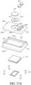
- Figure 17A is a schematic exploded view of the device 5 illustrated in Figures 16A-16F as seen from above.
- Figure 17B is a schematic exploded view of the device 5 illustrated in Figures 16A-16F as seen from below.
- Figure 18A is a schematic perspective view of the lower portion 134 of the device 5 illustrated in Figures 16A-17B .
- Figure 18B is a schematic bottom plan view of the lower portion 134 illustrated in Figure 18A .
- Figure 18C is a schematic side view of the lower portion 134 illustrated in Figures 18A and 18B with the molding.
- Figure 19A is a schematic bottom plan view of the upper portion 132 of the device 5 illustrated in Figures 16A-17B .
- Figure 19B is a schematic perspective view of the upper portion 132 illustrated in Figure 19A .
- Figure 19C is a schematic side view of the upper portion 132 illustrated in Figures 19A and 19B .
- Figure 20A is a schematic perspective view of the membrane 138 of the device 5 illustrated in Figures 16A-17B .
- Figure 20B is a schematic perspective view of the filter 139 of the device 5 illustrated in Figures 16A-17B .
- the membrane 138 can comprise a plurality of layers.
- the membrane 138 can include a membrane body or a hydrophobic layer 151 (e.g., PTFE) and adhesive layer 153.
- the adhesive layer 153 can adhere the membrane 138 to the upper portion 132 of the housing 130 over the access port 136.
- the adhesive layer 153 can adhere the membrane 138 to a recess formed at the bottom side 132b of the upper portion 132 and over the access port 136.
- the adhesive layer 153 can adhere the membrane 138 to the upper side 132a of the upper portion 132 over the access port 136.
- the filter 139 can include a filter layer 150 and an adhesive layer 152.
- the adhesive layer 152 can adhere the filter layer 150 to a recess formed in the upper portion 132 of the housing 130 and over the access port 136.
- the access port 136 can be structured such that when the filter 139 is placed in the access port 136, the top side 132a of the upper portion 132 can be generally planar.
- the filter layer 150 can comprise any suitable materials.
- the filter 139 can include any suitable additional layers. In some applications, the filter 139 can filter unwanted materials that might interfere with detection of the gas(es) of interest.
- the filter 139 can comprise activated carbon that can react with alcohol (e.g., adsorb alcohol).
- the filter 139 can comprise activated woven carbon cloth.
- the activated woven carbon cloth can be Flexzorb TM ACC, manufactured by Chemviron, for all of the embodiments herein that include a filter.
- the lower portion 134 can include a plurality of holes 154 for conductive plugs 156.
- the conductive plugs 156 can comprise, for example, a solder plug or a conductive epoxy plug.
- the conductive plug 156 can be connected to ends 147a of the arms 147 formed in the upper portion 132.
- Figure 21A is a schematic top plan view of a lead frame structure 160 according to one embodiment.
- Figure 21B is a schematic side view of the lead frame structure 160 illustrated in Figure 21A .
- Figure 21C is a schematic bottom perspective view of the lead frame structure 160 illustrated in Figures 21A and 21B .
- the lead frame structure 160 can comprise the plurality of electrodes 145, and the arms 147 that extends from the electrodes 145.
- the ends 147a of the arms 147 and/or the electrodes 145 can be coated with a protective layer (e.g., a gold layer).
- the electrodes 145 can be coated with a carbon black or other catalyst layer.
- the lead frame structure 160 can comprise various metal materials, such as copper, stainless steel, etc.
- the lead frame structure 160 can comprise conductive non-metal materials, such as conductive ABS.
- a method of manufacturing a device as defined by claims 13 or 14 includes fabricating a housing that has an upper portion and a lower portion.
- the method can include fabricating a lead frame that has a plurality of electrodes and arms extending from the electrodes.
- Fabricating the housing includes a molding process, for example, single or double shots molding.
- fabricating the lead frame can include providing a conductive plastic material in voids or grooves formed in a the housing.
- the housing can be defined by a molding material (e.g., liquid crystal polymer (LCP) or acrylonitrile butadiene styrene (ABS)).
- LCP liquid crystal polymer
- ABS acrylonitrile butadiene styrene
- fabricating the housing can include ovemolding the lead frame (metal or conductively-filled plastic) by a molding material (e.g., LCP or ABS).
- fabricating the housing can include providing the upper portion (e.g., a first element) and providing the lower portion (e.g., a second element).
- the lower portion can have a chamber configured to receive an electrochemical solution.
- the upper portion can have a plurality of electrodes, an access port, and/or a fill port.
- fabricating the housing can include bonding the upper potion and the lower portion.
- the upper portion and the lower portion can be bonded by way of an adhesive.
- the upper portion and the lower portion can be monolithically formed.
- fabricating the housing can include providing a seal plate configured to seal the chamber.
- the method includes also providing a membrane and optionally also a filter to the access port.
- the membrane allows gas communication between the chamber and the outside environs while preventing liquid communication between the chamber and the outside environs.
- the membrane can be attached to the housing by way of an adhesive, ultrasonic welding, or thermal welding.
- the method can also include filling an electrochemical solution into the chamber.
- the electrochemical solution can be filled into the chamber through the fill port.
- the fill port can be sealed by way of a plug, and/or epoxy, potting materials.
- the method can also include forming an interconnect structure in the device.
- the lower potion can include a through via (e.g., through mold via) that can at least partially provide interconnection between the plurality of electrodes to an external substrate or an external device.
- the method also includes providing a system in package (SiP).
- SiP can be provided into a cavity formed in the housing.
- the cavity can be formed in the lower portion of the housing.
- SiP can be over molded directly into the lower portion of the package.
Landscapes
- Chemical & Material Sciences (AREA)
- Life Sciences & Earth Sciences (AREA)
- Health & Medical Sciences (AREA)
- Engineering & Computer Science (AREA)
- General Physics & Mathematics (AREA)
- Pathology (AREA)
- Immunology (AREA)
- General Health & Medical Sciences (AREA)
- Biochemistry (AREA)
- Analytical Chemistry (AREA)
- Physics & Mathematics (AREA)
- Electrochemistry (AREA)
- Chemical Kinetics & Catalysis (AREA)
- Molecular Biology (AREA)
- Combustion & Propulsion (AREA)
- Food Science & Technology (AREA)
- Medicinal Chemistry (AREA)
- Sustainable Development (AREA)
- General Chemical & Material Sciences (AREA)
- Manufacturing & Machinery (AREA)
- Sustainable Energy (AREA)
- Electrolytic Production Of Non-Metals, Compounds, Apparatuses Therefor (AREA)
Description
- The field relates to electrochemical devices, and, in particular, to gas sensor devices.
- Electrochemical devices can include electrochemical sensor devices. An electrochemical sensor device can observe chemical reactions by monitoring changes in electrical properties (e.g., voltage and current). The electrochemical sensor device can be a gas sensor device for detecting gases. The electrochemical sensor device can include an electrochemical solution or material and electrodes.
EP 3 480 590 A1 discloses a gas sensor package including a housing defining a first chamber and a second chamber with the electrolyte being provided in the first chamber.US 7 077 938 B1 discloses an electrochemical gas sensor having a planar substrate with at least one planar electrode formed thereon and a housing defining a reservoir containing an electrolyte.US 2012/065617 A1 discloses a configuration for a sensor for immittance spectroscopy. - In one aspect, a gas sensor is disclosed according to
claim 1. - In one embodiment, the gas sensor can also include a microcontroller packaged in the housing and electrically coupled to the plurality of electrodes.
- In one embodiment, the housing includes polymer or plastic.
- In one embodiment, at least one of the plurality of electrodes includes conductive non-metal materials filled with carbon fiber.
- In one embodiment, the gas sensor further includes conductive arms extending horizontally from the plurality of electrodes. A thickness of the electrode can be greater than a thickness of the conductive arms. The plurality of electrodes can be in electrical communication with an interconnect structure that is formed in the housing. The interconnect structures can include the conductive arms and a plurality of interconnects that extend at least partially through the lower portion from a top side of the lower portion.
- In one embodiment, the housing includes a fill port that is sealed. The electrochemical solution can be disposed in the chamber through the fill port.
- The access port includes a membrane that allows gas communication between the chamber and the outside environs while preventing liquid communication between the chamber and the outside environs.
- In one embodiment, the lower portion of the housing further includes a cavity that is separate from the chamber. The cavity can be configured to receive an electrical component. The cavity can be configured to receive a plurality of electrical components.
- In one embodiment, the plurality of electrodes include or more of carbon black, iridium black, platinum black, gold black, or ruthenium black.
- In one aspect, a gas sensor is disclosed according to claim 8.
- In one embodiment, the housing includes polymer or plastic molded over the plurality of electrodes.
- In one embodiment, the access port is configured to provide fluid communication between the chamber and the outside environs.
- The access port includes a membrane that allows gas communication between the interior of the housing and the outside environs while preventing liquid communication between the interior of the housing and the outside environs.
- In one embodiment, the plurality of electrodes are in electrical communication with an interconnect structure formed in the lower portion of the housing. The interconnect structures can include a plurality of interconnects extending at least partially through the lower portion from a top side of the lower portion.
- In one embodiment, the lower portion of the housing further includes a cavity that is separate from the chamber. The cavity can be configured to receive an electrical component. At least a portion of the upper portion of the housing can be covered with the catalytic material.
- In one aspect, a method of manufacturing a gas sensor is disclosed according to claim 13.
- In another aspect, a method of manufacturing a gas sensor is disclosed according to
claim 14. - Embodiments of this disclosure will now be described, by way of non-limiting example, with reference to the accompanying drawings.
-
Figure 1A is a schematic top perspective view of a device according to one embodiment. -
Figure 1B is a schematic bottom perspective view of the device illustrated inFigure 1A . -
Figure 2A is a schematic side view of the device illustrated inFigures 1A and1B . -
Figure 2B is a schematic side view of the device illustrated inFigures 1A-2A with internal components of the device shown in dashed lines. -
Figure 3A is a schematic top perspective view of the device illustrated inFigures 1A-2B with internal components of the device shown in dashed lines. -
Figure 3B is a schematic bottom perspective view of the device illustrated inFigures 1A-3A with internal components of the device shown in dashed lines. -
Figure 4A is a schematic exploded view of the device illustrated inFigures 1A-3B as seen from a perspective view from above. -
Figure 4B is a schematic exploded view of the device illustrated inFigures 1A-4A as seen from a perspective view from below. -
Figure 5A is a schematic perspective cut-away view of the device ofFigures 1A-4B . -
Figure 5B is an enlarged view of a portion ofFigure 5A . -
Figure 6A is a schematic top perspective view of an upper portion of a housing. -
Figure 6B is a view of the upper portion ofFigure 6A with components within the upper portion shown in dashed lines. -
Figure 6C is a schematic bottom, exploded perspective view of the upper portion ofFigure 6A with solder balls separated from the upper portion. -
Figure 7A is a schematic top perspective view of a lead frame that includes electrodes and arms for use within the housing ofFigures 1A-6C , according to one embodiment. -
Figure 7B is a schematic bottom perspective view of the lead frame illustrated inFigure 7A . -
Figure 8A is a schematic top perspective view of a device according to another embodiment. -
Figure 8B is a schematic bottom perspective view of the device illustrated inFigure 8A . -
Figure 8C is a schematic side view of the device illustrated inFigures 8A and8B . -
Figure 8D is a schematic side view of the device with internal components of the device shown in dashed lines. -
Figure 9A is a schematic top perspective view of a device according to another embodiment. -
Figure 9B is a schematic bottom perspective view of the device illustrated inFigure 9A . -
Figure 9C is a schematic bottom perspective view of the device illustrated inFigures 9A and9B with a lower seal plate omitted. -
Figure 9D is a schematic side view of the device illustrated inFigures 9A and9B . -
Figure 9E is a schematic side view of the device with internal components of the device shown in dashed lines. -
Figure 10A is a schematic top perspective view of a device according to another embodiment. -
Figure 10B is a schematic bottom perspective view of the device illustrated inFigure 10A . -
Figure 10C is a schematic top perspective view of the device with internal components of the device shown in dashed lines. -
Figure 10D is a schematic bottom perspective view of the device with a lower portion and a printed circuit board assembly (PCBA) and internal components in the device shown in dashed lines. -
Figure 11A is a schematic exploded view of the device illustrated inFigures 10A-10D as seen from a perspective view from above. -
Figure 11B is a schematic exploded view of the device illustrated inFigures 10A-10D as seen from a perspective view from below. -
Figure 12 is a schematic perspective cut-away view of the device ofFigures 10A-11B . -
Figure 13A is a bottom plan view of an upper portion of the device ofFigures 10A-11B . -
Figure 13B is a schematic perspective view of the upper portion illustrated inFigure 13A with internal components of the upper portion shown in dashed lines. -
Figure 13C is a schematic perspective view of a membrane according to one embodiment. -
Figure 14A is a schematic top plan view of a lead frame structure for an electrochemical sensor according to one embodiment. -
Figure 14B is a schematic side view of the lead frame structure illustrated inFigure 14A . -
Figure 14C is a schematic bottom perspective view of the lead frame structure illustrated inFigures 14A and14B . -
Figure 15A is a schematic perspective view of a system in package (SiP) according to one embodiment. -
Figure 15B is a schematic bottom plan view of the SiP illustrated inFigure 15A . -
Figure 15C is a schematic perspective view of the SiP ofFigures 15A-15B with internal components in the SiP shown in dashed lines. -
Figure 16A is a schematic top perspective view of a device according to another embodiment. -
Figure 16B is a schematic bottom perspective view of the device illustrated inFigure 16A . -
Figure 16C is a schematic top perspective view of the device ofFigures 16A-16B with internal components of the device shown in dashed lines. -
Figure 16D is a schematic bottom perspective view of the device ofFigures 16A-16C with internal components of the device shown in dashed lines. -
Figure 16E is a schematic perspective cut-away view of the device ofFigures 16A-16D . -
Figure 16F is a schematic perspective view of another cut-away view of the device ofFigures 16A-16E . -
Figure 17A is a schematic exploded view of the device illustrated inFigures 16A-16F as seen from an angle. -
Figure 17B is a schematic exploded view of the device illustrated inFigures 16A-16F as seen from another angle. -
Figure 18A is a schematic perspective view of a lower portion of the device illustrated inFigures 16A-17B . -
Figure 18B is a schematic bottom plan view of the lower portion illustrated inFigure 18A . -
Figure 18C is a schematic side view of the device illustrated inFigures 16A-17B with internal components of the device shown in dashed lines. -
Figure 19A is a schematic bottom plan view of the upper portion of the device illustrated inFigures 16A-17B . -
Figure 19B is a schematic perspective view of the upper portion illustrated inFigure 19A , with internal components of the upper portion shown in dashed lines. -
Figure 19C is a schematic side view of the upper portion illustrated inFigures 19A and19B with internal components of the device shown in dashed lines. -
Figure 20A is a schematic perspective view of a membrane for the device illustrated inFigures 16A-17B . -
Figure 20B is a schematic perspective view of a filter of the device illustrated inFigures 16A-17B . -
Figure 21A is a schematic top plan view of a lead frame structure for an electrochemical sensor according to one embodiment. -
Figure 21B is a schematic side view of the lead frame structure illustrated inFigure 21A . -
Figure 21C is a schematic bottom perspective view of the lead frame structure illustrated inFigures 21A and21B . - Electrochemical devices disclosed herein may be used as sensors. For example, an electrochemical device disclosed herein can be a gas sensor. Electrochemical devices disclosed herein can be manufactured using, for example, compact packaging platforms, such as a lead frame package, a ball grid array (BGA) package, and a land grid array (LGA) package. The electrochemical device can be used in, for example, a mobile device.
- An electrochemical device can include a chamber for receiving a liquid or wicking material. The chamber can receive, for example, an electrochemical material or solution (e.g., sulfuric acid). The electrochemical device can also include electrodes that are in contact with the electrochemical material. The electrodes can detect changes in electrical properties (e.g., voltage and current) of the electrochemical material due to an electrochemical material reaction. For example, the electrochemical material can react with gas. In some applications, the electrochemical device can be used to detect harmful gas (e.g., carbon monoxide) in an area.
- In certain manufacturing processes, it can be difficult to manufacture relatively small electrochemical devices, and/or manufacture relatively small electrochemical devices with relatively low cost. Some electrochemical devices disclosed herein can include a housing that is at least partially defined by a molded lead frame. Such electrochemical devices with a molded lead frame can be manufactured using a relatively low cost manufacturing method, such as a molding process. Also, the molding process can be suitable for manufacturing relatively small electrochemical devices at much lower expense compared to other technologies for small electrochemical devices.
- Various embodiments disclosed herein relate to an electrochemical device. In one aspect, an electrochemical device can include a housing that has an upper portion and a lower portion. The upper portion can be a first element and the lower potion can be a second element that is attached to the first element, in some embodiments. The electrochemical device can also include a chamber formed in the lower portion of the housing. The chamber can receive an electrochemical solution. In some embodiments, the electrochemical solution includes sulfuric acid, which advantageously has relatively high conductivity and water content for aiding electrochemical reactions. The electrochemical solution can react with molecules, such as gas molecules. The electrochemical solution can change its electrical properties (e.g., voltage or current) due to the reaction(s) with the molecules. In some embodiments, the electrochemical solution can react with the molecules indirectly via a catalyst. The electrochemical device can also include a plurality of electrodes formed in the upper portion of the housing. The plurality of electrodes can be exposed to the chamber. In some embodiments, the plurality of electrodes can include a sensing electrode, counter electrode, and/or a reference electrode. The plurality of electrodes can include a catalyst that react with the electrochemical solution and/or the target molecules. Oxidation and/or reduction reactions can occur at an interface between the catalyst and the electrochemical solution. The plurality of electrodes can detect or monitor the changes in electrical properties of the electrochemical solution. The monitored electrical properties can be analyzed and/or processed to determine the molecules that reacted with the electrochemical solution. The electrochemical device can further include an access port formed in the upper portion of the housing. The access port can provide fluid communication between the interior of the housing (e.g., the chamber) and the outside environs. Therefore, in some embodiments, the gas molecules can access the interior of the housing (e.g., the chamber or the electrode) through the access port.
-
Figure 1A is a schematic top perspective view of adevice 1 according to one embodiment.Figure 1B is a schematic bottom perspective view of thedevice 1 illustrated inFigure 1A . For example, thedevice 1 can be used as an electrochemical device, such as a gas sensor. Thedevice 1 can include ahousing 10 that has anupper portion 12 and alower potion 14. In the illustrated embodiment, theupper portion 12 and thelower portion 14 can be separate elements. For example, theupper portion 12 can be defined by a second element and thelower portion 14 can be defined by a first element that is coupled to the second element. In such embodiments, theupper portion 12 and thelower portion 14 can be bonded by an adhesive, and/or other bonding methods, such as ultrasonic bonding. Theupper portion 12 and thelower portion 14 can be manufactured separately, in some embodiments. - The
housing 10 can comprise any suitable material. In some embodiments, thehousing 10 can comprise a molding material, such as plastic or polymer (e.g., liquid crystal polymer (LCP) or acrylonitrile butadiene styrene (ABS)). Thehousing 10 has a generally cuboid shape. However, thehousing 10 can have any suitable shape. In some embodiments, the upper portion can comprise conductors integrated with the plastic, such as a molded metal lead frame, or a molded lead frame with conductive non-metal materials, such as conductive ABS, embedded in a non-conductive plastic mold. - The
housing 10 ofdevice 1 can have alength 11, a width w1, and a height (a height h1 of theupper portion 12 plus a height h2 of the lower portion 14). In some embodiments, thelength 11 of thehousing 10 can be in a range of, for example, 5 mm to 25 mm, in a range of, for example, 10 mm to 25 mm, in a range of, for example, 5 mm to 20 mm, or in a range of, for example, 10 mm to 20 mm. In some embodiments, the width w1 of thehousing 10 can be in a range of, for example, 5 mm to 25 mm, in a range of, for example, 10 mm to 25 mm, in a range of, for example, 5 mm to 20 mm, or in a range of, for example, 10 mm to 20 mm. In some embodiments, the height h1 of theupper portion 12 can be in a range of, for example, 0.5 mm to 3 mm, in a range of, for example, 1 mm to 3 mm, in a range of, for example, 0.5 mm to 2 mm, or in a range of, for example, 1 mm to 2 mm. In some embodiments, the height h2 of thelower portion 14 can be in a range of, for example, 0.5 mm to 3 mm, in a range of, for example, 1 mm to 3 mm, in a range of, for example, 0.5 mm to 2 mm, or in a range of, for example, 1 mm to 2 mm. - The
upper portion 12 of thehousing 10 has atop side 12a and abottom side 12b opposite thetop side 12a. Thelower portion 14 of the housing has atop side 14a and abottom side 14b opposite thetop side 14a. Thebottom side 12b of theupper portion 12 and thetop side 14a of thelower portion 14 can be coupled together. In some embodiments, thebottom side 12b of theupper portion 12 and thetop side 14a of thelower portion 14 can be bonded by way of an adhesive, and/or other bonding methods, such as ultrasonic welding. In some embodiments, thetop side 12a of theupper potion 12 can define atop side 10a of thehousing 10. In some embodiments, thebottom side 14b of thelower potion 14 can define abottom side 10b of thehousing 10. - As illustrated in
Figure 1A , thedevice 1 includes anaccess port 16 formed in theupper portion 12 of thehousing 10. In some embodiments, thedevice 1 can include more than one access port. Theaccess port 16 provides fluid communication between an interior of thedevice 1 and the outside environs. Amembrane 18 is provided in theaccess port 16. Themembrane 18 allows gas to pass through while preventing liquid from passing through, thus retaining electrolyte in the cavity, while allowing analyte gases to pass. - The
device 1 can also include aplug 20 that seals a fill port 28 (seeFigure 2B ). Theplug 20 can be made of the same of a different material as the material of thehousing 10. For example, the plug can comprise a molding material such as liquid crystal polymer (LCP) or acrylonitrile butadiene styrene (ABS). The fill port can be used for filling a filler material (e.g., an electrochemical solution) into a chamber defined in thedevice 1. Theplug 20 can comprise epoxy or potting materials that are compatible or non-reactive with the electrochemical solution. - As illustrated in
Figure 1B , thedevice 1 can also include a plurality ofleads 22 on thebottom side 10b of thehousing 10. In some embodiments, theleads 22 can be configured to attach to a substrate (e.g., printed circuit board (PCB)), or another device, thereby connecting thedevice 1 with the substrate or the device. For example, theleads 22 can be formed of balls of solder material such that thebottom side 10b of the housing serves as a ball grid array (BGA) connection to lower elements of an electrical system, such as a circuit board. -
Figure 2A is a schematic side view of thedevice 1 illustrated inFigures 1A and1B . Theplug 20 can protrude relative to thetop side 10a of thehousing 10, in thedevice 1 illustrated inFigure 2A . However, in some embodiments theplug 20 can be generally flush with the top side of 10a of thehousing 10. The leads 22 can protrude relative to thebottom side 10b of thehousing 10. -
Figure 2B is a schematic side view of thedevice 1 illustrated inFigures 1A-2A . As illustrated inFigure 2B , thedevice 1 includes achamber 24 that can be formed in thelower portion 14 of thehousing 10. Thedevice 1 includes also a plurality ofelectrodes 26 that are formed in theupper portion 12 of thehousing 10. Alternatively or in addition, the plurality ofelectrodes 26 can be formed in thelower portion 14 of thehousing 10, in some examples, however, the formation of electrodes in thelower portion 14 is not covered by the claims. The plurality ofelectrodes 26 can be at least partially exposed to thechamber 24. In some embodiments, theelectrodes 26 can include a sensing electrode, counter electrode, and/or a reference electrode, which are provided with separate interconnects to connect each sensor to an internal or external processor. In some embodiments, the electrodes can include a circle electrode and a half-moon electrode. - In some embodiments, the
chamber 24 can receive a filler material (e.g., an electrochemical solution). Thechamber 24 can be fully or partially filled with the electrochemical solution. Theaccess port 16 can provide fluid communication between thechamber 24 and the outside environs. For example, gas (e.g., carbon monoxide) can enter thechamber 24 through theaccess port 16. In some embodiments, theaccess port 16 can allow gas transmission but prevent liquid transmission to keep the electrochemical solution within thedevice 1. The gas entering into thechamber 24 can react with the electrochemical solution disposed in thechamber 24. In some embodiments, the gas entering into thechamber 24 can react with the electrochemical solution disposed in thechamber 24 at a catalyst surface interface. The filler material can include a wicking material, which is typically a compressible material. The design of the interior surfaces of the housing can include features that compress the wicking material at the locations of the plurality of electrodes 26 (e.g., a surface of the catalyst of the electrodes), thereby ensuring wetting the plurality ofelectrodes 26 with the electrochemical solution. The wicking material can be applied to any of the electrodes disclosed herein. - In some embodiments, the electrochemical solution can be provided into the
chamber 24 through afill port 28 formed in theupper portion 12 of thehousing 10. Alternatively or in addition, thefill port 28 can be formed in thelower portion 14 of thehousing 10, in some embodiments. Thefill port 28 can be sealed with theplug 20. In some embodiments, theplug 20 can comprise epoxy, potting materials, or tapes with an acid compatible adhesive that are compatible or non-reactive with the electrochemical solution, after the electrochemical solution has been provided into thechamber 24. In some embodiments, the electrochemical solution can be provided after theupper portion 12 and thelower portion 14 are bonded together to define thehousing 10. Certain bonding processes apply heat with relatively high temperature for bonding. Therefore, in some embodiments, providing the electrochemical solution into thechamber 24 after bonding can prevent the electrochemical solution from being heated to a relatively high temperature during the bonding process. - As explained above, the
membrane 18 within theaccess port 16 allows gas to pass through while preventing liquid from passing through. Themembrane 18 prevents the electrochemical solution from leaking outside of thedevice 1. Therefore, thechamber 24 can be at least partially sealed by themembrane 18 from the outside environs while being fluidly communicative with the outside environ for gas sensing applications. Themembrane 18 can comprise a commercially available gas-permeable and liquid impermeable membrane, such as those manufactured by W.L. Gore & Associates, Inc. (Newark, DE). - The plurality of
electrodes 26 can be in contact with the electrochemical solution in thechamber 24. In some embodiments, the plurality ofelectrodes 26 can be used to monitor changes in electrical properties of the electrochemical solution due to chemical reactions. The observed changes in electrical properties of the electrochemical solution can be analyzed and/or processed to determine the molecules of the gas that enter thechamber 24. - In some embodiments, the plurality of
electrodes 26 can comprise a metal lead frame (e.g., a copper lead frame), or a lead frame embedding conductive non-metallic materials, such as conductive ABS. In some embodiments, the plurality ofelectrodes 26 can be connected to an interconnect structure. The interconnect structure can includearms 30 that horizontally extend at least partially through theupper portion 12 of thehousing 10. The interconnect structure can include vertical interconnects (e.g., solder plugs 32). The solder plugs 32 can extend at least partially through thelower portion 14 of thehousing 10. In some embodiments, the solder plugs 32 can extend through thelower portion 14 of the housing from thetop side 14a to thebottom side 14b of thelower portion 14. The leads 22 can be provided to the corresponding solder plugs 32. In some embodiments, theleads 22, such as BGA solder balls, can electrically and/or mechanically connect the solder plugs 32 to an external substrate (e.g., printed circuit board (PCB)) or another device. -
Figure 3A is a schematic top perspective view of thedevice 1 illustrated inFigures 1A-2B .Figure 3B is a schematic bottom perspective view of thedevice 1 illustrated inFigures 1A-3A . Thearms 30 that extend from the plurality ofelectrodes 26 can horizontally extend at least partially through theupper portion 12 of thehousing 10 in various directions. For example, as illustrated inFigure 3A , there can be threeelectrodes 26 and sixarms 30 that extend outwardly from the threeelectrodes 26 to near edges of the housing 10 (e.g., between thechamber 24 and outer edges of the housing 10). As will be better understood from illustrations described below, for metal lead frame embodiments, thearms 30 can represent half-etched portions of a lead frame that are embedded in molding, whereas the electrode portions and contacts (arm ends 30a) to the vertical interconnects (solder plugs 32) can be thicker portions of the lead frame that are exposed by the mold material of theupper portion 12. In some embodiments where conductive non-metallic materials or conductively-filled plastics are used as theelectrodes 26, theelectrodes 26 and thehousing 10 can be separately molded and bonded together, or double molded together (conductively-filled plastic can be first molded in the shape of the lead frame, and overmolded with an insulating plastic, or the insulating housing can be first molded and the conductive plastic interconnects and electrodes molded subsequently into voids in the housing). The conductive filler of the conductively-filled plastic can include, for example, carbon in the form of, for example, fibers or particles, or metal in the form of particles. The conductively-filled plastic can be applied to any of the electrodes disclosed herein in place of the metal of a conventional lead frame. - The
device 1 can comprise avolume expansion feature 34. Thevolume expansion feature 34 can accommodate volume expansion of the electrochemical solution that is disposed in thechamber 24. For example, the electrochemical solution may expand when reacted with gas molecules. In some embodiments, the electrochemical solution can comprise a hygroscopic material and may change its volume due to change in, for example, humidity. For example, where the electrolyte comprises sulfuric acid, the volume may change with the ambient humidity. The expanded volume of the electrochemical solution can escape into thevolume expansion feature 34 thereby mitigating the risk of, for example, excess pressure in the chamber, which might adversely affect themembrane 18 or plug 20. Thevolume expansion feature 34 can comprise a recess or cavity formed on thebottom side 12b of theupper portion 10. A size of thevolume expansion feature 34 can be selected based at least in part on a difference between a volume of the electrochemical solution under maximum and minimum humidity conditions. -
Figure 4A is a schematic exploded view of thedevice 1 illustrated inFigures 1A-3B as seen from an angle.Figure 4B is a schematic exploded view of thedevice 1 illustrated inFigures 1A-4A as seen from another angle. In some embodiments, theupper portion 12 and thelower portion 14 can comprise two separate elements. In such embodiments, theupper portion 12 and thelower portion 14 can be separately manufactured and bonded together to define thehousing 10. In some embodiments, theupper portion 12 and thelower portion 14 can be bonded by way of an intervening adhesive, or some other methods, such as ultrasonic welding. - The
chamber 24 can have any suitable shape. In some embodiments, thechamber 24 can include one or more protrusions to compress the wicking material (when the wicking material is used). The protrusion(s) can be located on the lower portion of the chamber, opposite theelectrodes 26. By compressing the wicking material against the plurality ofelectrodes 26, an improved capillary/wicking action can be provided. This way, the electrode wetting can be more consistent than thechamber 24 without the protrusion, independently of the electrolyte state-of-health and device orientation. - The
lower portion 14 can comprise a plurality of throughholes 36 for the vertical interconnects (e.g., solder plugs 32). In some embodiments, the throughholes 36 can be formed prior to providing the solder plugs 32. For example, the throughholes 36 can be formed by way of drilling. In some embodiments, the throughholes 36 can be formed as thelower portion 14 is formed. For example, the vertical interconnects can be first formed and then overmolded when thelower portion 14 is formed, similar to the embedded lead frame of theupper portion 12. - The
upper portion 12 of thehousing 10 can include connectors 38 (e.g., solder balls) on thebottom side 12b. Theconnectors 38 can be provided to corresponding ends of the arm 30 (see, for example,Figures 6B and6C ). Theconnectors 38 can electrically and/or mechanically connect with the vertical interconnects (solder plugs 32). In some embodiments, theconnectors 38 can help bonding theupper portion 12 and thelower portion 14. -
Figure 5A is a schematic perspective cut-away view of thedevice 1.Figure 5B is an enlarged view of a portion ofFigure 5A . The cross section of thedevice 1 shows thechamber 24 formed in thelower portion 14 of thehousing 10, theelectrodes 26 formed in theupper portion 12 of thehousing 10, thefilter 18 provided in theaccess port 16 formed in theupper portion 12, and theplug 20 that seals thefill port 28 formed in theupper portion 12. - As illustrated in
Figures 5A and5B , theelectrodes 26 can be at least partially exposed to thechamber 24. At least a portion of theelectrodes 26 that is not exposed to thechamber 24 can be embedded in the molding of theupper portion 12. Thearms 30 shown inFigures 3A and3B can be thinner than theelectrodes 26 and thus embedded in the molding of theupper portion 12. In some embodiments, theelectrodes 26 can be positioned near theaccess port 16. Theelectrodes 26 can be spaced apart by the molding material of theupper portion 12 of thehousing 10. In some embodiments, theelectrodes 26 can be generally flush with thebottom side 12b of theupper portion 12. In some embodiments, theelectrodes 26 can protrude relative to thebottom side 12b of theupper portion 12, such that at least a portion of theelectrodes 26 is disposed within thechamber 24. While not illustrated inFigures 4B-5B , it will be understood from the description below that a catalyst layer can coat the underside of the electrodes and can also coat portions of the underside of the insulating plastic of theupper portion 12. - In some embodiments, the
membrane 18 can comprise a plurality of layers. For example, themembrane 18 can include a membrane body 40 (e.g., a polytetrafluoroethylene (PTFE) membrane),adhesive layers 42, and aprotective layer 44. In some embodiments, a cross-interference filter (not illustrated for this embodiment) can also be located at the access port outside themembrane 18. One of theadhesive layers 42 can adhere themembrane 18 to theupper portion 12 of thehousing 10. In some embodiments, as illustrated, theadhesive layer 42 can adhere themembrane 18 to thetop side 12a of theupper portion 12. In some other embodiments, theadhesive layer 42 can adhere themembrane 18 to thebottom side 12b of theupper portion 12. Theadhesive layer 42 can be strong enough to prevent leakage of the electrochemical solution provided in thechamber 24. - The
plug 20 can seal the chamber from outside environs after disposing the electrochemical solution into thechamber 24. In some embodiments, an adhesive (not illustrated) can be provided between theplug 20 and theupper portion 12 of thehousing 10. In some embodiments, theplug 20 can include an encapsulation (not illustrated) to mitigate a risk of leakage of the electrochemical solution. In some other embodiments, epoxy or potting materials that are not reactive with the electrochemical solution can be used to seal the chamber. -
Figure 6A is a schematic perspective view of theupper portion 12 of thehousing 10 without themembrane 18 and theplug 20. The access port 16 (defined in part by a central working or sensing ring electrode embedded in plastic), thefill port 28, the plurality ofelectrodes 26, and thearms 30 can be formed in theupper portion 12. Theelectrodes 26 and thearms 30 can be at least partially embedded (e.g., molded) in theupper portion 12. -
Figure 6C is a schematic perspective view of theupper portion 12 and the connectors 38 (e.g. solder balls). Theconnectors 38 can be provided tocorresponding ends 30a of thearms 30 shown inFigure 6C . In some embodiments, theends 30a of thearms 30 and/or theelectrodes 26 can be coated with a protective layer (e.g., a gold layer). The gold layer can help prevent the base material of lead frame that forms the arm and the electrodes from oxidation. In some embodiments, a coating material can comprise catalyst. In some embodiments, theelectrodes 26 can be aluminum or copper base material coated with a catalytic material such as carbon black, iridium black , a platinum black gold black, and/or ruthenium black. The catalytic material can enhance the performance of theelectrode 26, in some applications. In some embodiments, different coating material(s) can be selected based at least in part on the gas(es) interested to be sensed. The coating material can be coated on theelectrodes 26 in any suitable manner. For example, a coating material (e.g., platinum black) can be coated on theelectrodes 26 by way of screen printing or stencil printing. In such processes, the coating material can be applied as an ink and can be applied over both the undersides of the electrodes and the insulating plastic of theupper part 18 after assembly of the upper part (including placement of themembrane 138 illustrated below). The ink can include hydrophobic particles, such as polytetrafluoroethylene (PTFE) or the line materials. The catalytic layer is illustrated below as the lowest layer of the electrodes exposed to the cavity, for example, inFigures 11A and13B , among others. The Catalyst layer can be applied in any of the embodiments disclosed herein. Though the catalyst material is not illustrated with the plurality ofelectrodes 26 inFigures 1A-9E , the catalyst material can be provided for theelectrodes 26 as illustrated and described in various embodiments disclosed herein. The catalyst material can be coated onto the inner surface of the housing in illustrated embodiments, includingFigures 1A-9E , after assembly of the upper portion of the housing, including the membrane and the filter (if present). The timing of the coating is such that the catalytic material individually coats each electrically separate electrode along with surrounding portions of insulating mold material. In the case of the working or sensing electrode, the catalytic coating can also cover and contact the membrane, ensuring contact of the analyte gas with the catalytic coating that serves as the working electrode. -
Figure 7A is a schematic top perspective view of alead frame 46 that includes theelectrodes 26 andarms 30, according to one embodiment. In some embodiments, thelead frame 46 can comprise a copper lead frame. In some embodiments, thelead frame 46 can comprise a conductive plastic lead frame. The conductive plastic lead frame can include a lead frame that comprises plastic (e.g., liquid crystal polymer (LCP) or acrylonitrile butadiene styrene (ABS)) and carbon fiber. In some embodiments, the carbon fiber or other conductive filler material can be mixed, embedded, or otherwise integrated with the plastic.Figure 7B is a schematic bottom perspective view of thelead frame 46 illustrated inFigure 7A . Thelead frame 46 can be at least partially embedded (e.g., molded) in theupper portion 12 of thehousing 10. In some embodiments, theelectrode 26 can have a curvature. For example, theelectrode 26 can have a round shape, a half-moon shape, and/or a circular shape. In some embodiments, a curved electrode can provide a shorter path through the electrolyte between electrodes (a first electrode and a second electrode) than with an electrode without curvature. When the path between the electrodes is shorter, there can be less resistance than with a longer path between the electrodes, thereby enhancing the accuracy of measurement of changes on electrical properties in the device. - The
arms 30 of thelead frame 46 have a width w2. In some embodiments, the width w2 can be in a range of, for example, 0.5 mm to 5 mm, in a range of, for example, 0.5 mm to 3 mm, or in a range of, for example, 0.8 mm to 1.2 mm. Thearms 30 of theleadframe 46 have a thickness t1 between theelectrodes 26 and theends 30a of thearms 30. The ends 30a of thearms 30 have a thickness t2. Theelectrodes 26 of thelead frame 46 have a thickness t3. In some embodiments, the thickness t1 of thearms 30 can be less than the thickness t2 of theends 30a and/or the thickness t3 of theelectrodes 26. Such an arrangement can be achieved by half-etching thearms 30 during lead frame fabrication so that they may be embedded during molding in polymer, such as LCP or ABS. In some embodiments, the thickness t1 of thearms 30 can be less than seventy percent (70%), between twenty percent (20%) to seventy percent (70%), or between forty percent (40%) to sixty percent (60%), of the thickness t2 of theends 30a and/or the thickness t3 of theelectrodes 26. For example, the thickness t1 of thearms 30 can be about fifty percent (50%). In some embodiments, the thickness t1 of thearms 30 can be in a range of, for example, 0.1 mm to 0.5 mm, in a range of, for example, 0.2 mm to 0.5 mm, or in a range of, for example, 0.1 mm to 0.3 mm. In some embodiments, the thickness t2 of theends 30a of thearms 30 can be in a range of, for example, 0.1 mm to 1 mm, in a range of, for example, 0.2 mm to 0.5 mm, or in a range of, for example, 0.3 mm to 0.7 mm. In some embodiments, the thickness t3 of theelectrodes 26 can be in a range of, for example, 0.1 mm to 1 mm, in a range of, for example, 0.2 mm to 0.5 mm, or in a range of, for example, 0.3 mm to 0.7 mm. As noted above, theelectrodes 26 also include a catalytic layer (not shown inFigure 7B ), such that the thicker portions of thelead frame 46 shown inFigures 7A and7B may be viewed as contacts for catalytic electrodes. -
Figure 8A is a schematic top perspective view of adevice 2 according to one embodiment.Figure 8B is a schematic bottom perspective view of thedevice 2 illustrated inFigure 8A .Figure 8C is a schematic side view of thedevice 2 illustrated inFigures 8A and8B . Unless otherwise noted, components of thedevice 2 may refer to components that are the same as or generally similar to like components of thedevice 1. Thedevice 2 is generally similar to thedevice 1. Instead of having a BGA structure ofdevice 1, thedevice 2 has a land grid array (LGA) structure. In other words, instead of having the BGA balls as theleads 22 on thebottom side 10b of thehousing 10, thedevice 2 comprises a plurality ofLGA pads 50 that are exposed on thebottom side 10b of thehousing 10. - The
device 2 can include ahousing 10 that has anupper portion 12 and alower portion 14, anaccess port 16 formed in theupper portion 12 of thehousing 10, achamber 24 formed in thelower portion 14 of thehousing 10, and a plurality ofelectrodes 26 formed in theupper portion 12 of thehousing 10. Thedevice 2 can also include amembrane 18 in a topside recess surrounding theaccess port 16. The device can also include aplug 20 that can seal afill port 28. Theplug 20 can protrude relative to thetop side 10a of thehousing 10. However, in some embodiments theplug 20 can be generally flush with the top side of 10a of thehousing 10. Alternatively, the plug can comprise epoxy or potting materials that are compatible or non-reactive with the electrochemical solution. Thebottom side 10b of thehousing 10 can be generally planar. -
Interconnects 52 can be formed in thelower portion 14 of thehousing 10. In some embodiments, theinterconnects 52 can extend through thelower portion 14 of thehousing 10 from thetop side 14a to thebottom side 14b of thelower portion 14. The exposed portion of theinterconnects 52 on thebottom side 14b of thelower portion 14 can define theLGA pads 50. In some embodiments, theLGA pads 50 can be coated with a protective layer (e.g., a gold layer). The embodiment ofFigures 8A-8B can be otherwise similar to the embodiment ofFigures 1A-7B . -
Figure 9A is a schematic top perspective view of a device 3 according to one embodiment.Figure 9B is a schematic bottom perspective view of the device 3 illustrated inFigure 9A .Figure 9C is a schematic bottom perspective view of the device 3 illustrated inFigures 9A and9B without aseal plate 54 and without the catalytic layers coating the electrodes and covering theaccess port 16.Figure 9D is a schematic side view of the device 3 illustrated inFigures 9A and9B . Unless otherwise noted, components of the device 3 may refer to components that are the same as or generally similar to like components of thedevices device 1 or a LGA structure ofdevice 2, the device 3 comprises a dual flat package (DFP) structure. In other words, instead of having the solder plugs and the BGA balls as the leads 22 (Figures 1A-7B ) or theinterconnects 52 and the LGA pads 50 (Figures 8A-8D ), the device 3 comprises leads formed bylegs 56 that extend from the housing 10'. - The device 3 can include a housing 10' that has an upper portion 12' and a lower portion 14', an
access port 16 formed in the upper portion 12' of the housing 10', a chamber 24' formed in the lower portion 14' of the housing 10', and a plurality ofelectrodes 26 formed in the upper portion 12' of the housing 10'. The device 3 can also include amembrane 18 and a filter (not shown) in theaccess port 16. The device can also include aplug 20 that can seal afill port 28. Theplug 20 can protrude relative to thetop side 10a' of the housing 10'. However, in some embodiments theplug 20 can be generally flush with the top side of 10a' of the housing 10'. Thebottom side 10b' of the housing 10' can be generally planar. Alternatively, theplug 20 can comprise epoxy or potting materials that are compatible or non-reactive with the electrochemical solution. The device 3 can also include theseal plate 54. - The upper portion 12' and the lower potion 14' of the housing 10' can be monolithically formed. In some embodiments the upper portion 12' and at least part of the lower portion 14' can be manufactured by a single molding process. The lower portion 14' can include the
seal plate 54 as a separate piece that can at least partially seal the chamber 24' from the outside environs. - The
legs 56 can extend from the upper portion 12' of the housing 10'. Thelegs 56 can be connected to the arms 30' and indeed can be integrally formed from the same lead frame. Thelegs 56 can be configured to connect to an external substrate (e.g., a printed circuit board (PCB)) or an external device. In some embodiments, the arms 30' and thelegs 56 can provide electrical pathway between theelectrodes 26 and the external substrate or the external device. Advantageously, all conductors for routing signals to and from theelectrodes 26 can be integrally formed by a single lead frame separate conductors and attendant fabrication steps for the lower portion 14' can be omitted. -
Figure 10A is a schematic top perspective view of a device 4 according to one embodiment.Figure 10B is a schematic bottom perspective view of the device 4 illustrated inFigure 10A . Unless otherwise noted, components of the device 4 may refer to components that are the same as or generally similar to like components of thedevices housing 60 that has anupper portion 62 and alower portion 64, anaccess port 65 formed in theupper portion 64 of thehousing 60, aplug 66 that can seal a fill port 80 (seeFigure 10C ) formed in theupper portion 64, and a printed circuit board assembly (PCBA) 68. Thehousing 60 can be coupled to a top side 68a of thePCBA 68. ThePCBA 68 can havecontact pads 70 at a bottom side 68b of thePCBA 68. In some embodiments, the device 4 can be configured to fit in a micro subscriber identification module (SIM) card socket. -
Figure 10C is a schematic top perspective view of the device 4 with internal components of the device 4.Figure 10D is a schematic bottom perspective view of the device 4 with thelower portion 64 and the dielectric portions of thePCBA 68. The device 4 can also include amembrane 72 formed in theupper portion 62 of thehousing 60, a plurality ofelectrodes 74 formed in theupper portion 62, achamber 76 formed in the upper part of thelower portion 64, and acavity 78 formed in the lower part of thelower portion 64. In some embodiments, themembrane 72 can include an adhesive layer. - The
upper portion 62 can be provided as a molded lead frame. Theelectrodes 74 can be exposed to thechamber 76. Thechamber 76 can receive an electrochemical solution. The electrochemical solution can be disposed into thechamber 76 through thefill port 80. Thefill port 80 can be sealed by way of theplug 66. Alternatively, the plug can comprise epoxy or potting materials that are compatible or non-reactive with the electrochemical solution. Theaccess port 65 can provide fluid communication between thechamber 76 and the outside environs through a gas-permeable and liquid impermeable membrane and a catalytic layer. - The
chamber 76 and thecavity 78 can be formed at different locations of thesecond portion 64. In some embodiments, thechamber 76 can be formed at thetop side 64a of thelower portion 64, and thecavity 78 can be formed at thebottom side 64b of thelower portion 64. Thecavity 78 can be configured to receive components disposed on thePCBA 68, such as processors and/or passive electronic components (e.g., resistors, capacitors, etc.). For example the PCBA can include a precision analog microcontroller with chemical sensor interface (e.g., ADuCM355 manufactured by Analog Devices Inc.). Thelower portion 64 can also includeinterconnects 82 that extend at least partially through thelower portion 64 from thetop side 64a. In some embodiments, theinterconnects 82 can extend through thelower portion 64 from thetop side 64a to thebottom side 64b. - In some embodiments, the
PCBA 68 can include a printed circuit board (PCB) 84 and a plurality ofcomponents 86 disposed on the PCB. Thecomponents 86 can include passive components and/or active components. In some embodiments, thecomponents 86 can process data acquired through theelectrodes 74. In some embodiments, one or more of thecomponents 86 can be electrically connected through an interconnect structure. The interconnect structure can includelead frame arms 88 that horizontally extends at least partially through theupper portion 62, and theinterconnects 82. In some embodiments, ends 88a ofarms 88 can be exposed on thebottom side 62 of theupper portion 62. In some embodiments, the interconnect structure can also include a trace (not illustrated) formed in or on thePCB 84. -
Figure 11A is a schematic exploded view of the device 4 illustrated inFigures 10A-10D as seen from above.Figure 11B is a schematic exploded view of the device 4 illustrated inFigures 10A-10D as seen from below. The lower portion can compriseholes 89 for receiving theinterconnects 82. In some embodiments,solder balls 90 can be provided to connect theinterconnects 82 andpads 92 on a top side 84a of thePCB 84. Theupper portion 62 can comprise avolume expansion feature 96, as explained above. - The
bottom side 62b of theupper portion 62 can comprise acoating material 75. In some embodiments, thecoating material 75 can comprise a catalyst such as carbon black, iridium black, platinum black gold black, and/or ruthenium black. Thus, theelectrodes 74 can include the conductors of the lead frame coated with catalytic material. The catalytic layer can enhance the performance of theelectrode 74, in some applications. In some embodiments, different coating material(s) 75 can be selected based at least in part on the gas(es) interested to be sensed. Thecoating material 75 can be coated on theelectrodes 74 in any suitable manner. For example, the coating material 75 (e.g., platinum black) can be coated on theelectrodes 74 and the plastic underside of theupper portion 62 of the housing by way of screen printing or stencil printing. In such processes, thecoating material 75 can be applied as an ink. The ink can include hydrophobic particles, such as polytetrafluoroethylene (PTFE) or the line materials. Thecatalytic coating material 75 can also cover the underside of themembrane 72 that communicates with theaccess port 65. -
Figure 12 is a schematic perspective cut-away view of the device 4. The cross section of the device 4 includes thechamber 76 formed at thetop side 64a of thelower portion 64, theelectrodes 74 formed in theupper portion 62, acavity 78 formed at thebottom side 64b of thelower portion 64, and theplug 66 that seals thefill port 80 formed in theupper portion 62. In some embodiments, thecavity 78 can have varying depths or heights for receiving different components having different heights. -
Figure 13A is a bottom plan view of theupper portion 62 of the device 4 without theplug 66.Figure 13B is a schematic perspective view of theupper portion 62 illustrated inFigure 13A with the molding of theupper portion 62. Theupper portion 62 can include themembrane 72, theelectrodes 74, thearms 88 that extends from theelectrodes 74 having arm ends 88', thefill port 80, and avolume expansion feature 96. In some embodiments, as illustrated, theelectrodes 74 can include the coating material 75 (such as carbon black), and thecoating material 75 can also cover themembrane 72. In some embodiments, the ends 88' of thearms 88 can be coated with a protective layer (e.g., a gold layer). As in the prior embodiments, thearms 88 can be half-etched portions of a lead frame, while the arm ends 88' andelectrodes 74 represent unetched thicker portions of the lead frame, or a conductively-filled plastic can be molded in these shapes. -
Figure 13C is a schematic perspective view of themembrane 72 according to one embodiment. Themembrane 72 can include anadhesive layer 100 and amembrane body 102. Themembrane 72 can also include a protective layer (not illustrated). The dimension of themembrane 72 can be selected such that the filter effectively seals thechamber 78 when provided in theupper portion 62. Themembrane 72 can also be embedded in the mold (e.g., LCP or ABS) of the molded lead frame that defines theupper portion 62 - The
membrane 72 has a diameter d1. In some embodiments, the diameter d1 of themembrane 72 can be in a range of, for example, 2.5 mm to 10 mm, in a range of, for example, 3 mm to 10 mm, in a range of, for example, 2.5 mm to 5 mm, or in a range of, for example, 3 mm to 5 mm. Themembrane 72 has a thickness t4. In some embodiments, the thickness t4 of themembrane 72 can be in a range of, for example, 0.2 mm to 0.5 mm, in a range of, for example, 0.3 mm to 0.5 mm, in a range of, for example, 0.2 mm to 0.4 mm, or in a range of, for example, 0.3 mm to 0.4 mm. - The
adhesive layer 100 has an inner diameter d2. In some embodiments, the inner diameter d2 of theadhesive layer 100 can be in a range of, for example, 1 mm to 5 mm, in a range of, for example, 1.5 mm to 5 mm, in a range of, for example, 0.5 mm to 3 mm, or in a range of, for example, 1.5 mm to 3 mm. - The
adhesive layer 100 has a thickness t5. In some embodiments, the thickness t5 of theadhesive layer 100 can be in a range of, for example, 0.05 mm to 0.5 mm, in a range of, for example, 0.08 mm to 0.5 mm, in a range of, for example, 0.05 mm to 0.2 mm, or in a range of, for example, 0.08 mm to 0.2 mm. - The
membrane body 102 has a thickness t6. In some embodiments, the thickness t6 of themembrane body 102 can be in a range of, for example, 0.2 mm to 0.5 mm, in a range of, for example, 0.3 mm to 0.5 mm, in a range of, for example, 0.2 mm to 0.4 mm, or in a range of, for example, 0.3 mm to 0.4 mm. -
Figure 14A is a schematic top plan view of alead frame structure 104 that can be included in any devices discloses herein.Figure 14B is a schematic side view of thelead frame structure 104 illustrated inFigure 14A .Figure 14C is a schematic bottom perspective view of thelead frame structure 104 illustrated inFigures 14A and14B . Thelead frame structure 104 can have similar functionality as thelead frame 46. Thelead frame structure 104 can comprise the plurality of electrodes 74 (thicker portions of thelead frame structure 104 in ring and arc shapes, as best seen inFigure 14C ), and thearms 88 that extend from theelectrodes 74. In some embodiments, the ends 88a of thearms 88 and/or theelectrodes 74 can be coated with a protective layer (e.g., a gold layer). In some embodiments, theelectrodes 74 can be coated with a carbon black layer, an iridium black layer, a platinum black layer gold black, ruthenium black or a mixture of such catalytic materials, such that the illustratedelectrodes 74 can be considered contacts to electrodes formed by the catalytic layer. -
Figure 15A is a schematic perspective view of a system in package (SiP) 110 that can be used with any of the devices disclosed herein, according to one embodiment.Figure 15B is a schematic bottom plan view of theSiP 110 illustrated inFigure 15A .Figure 15C is a schematic perspective view of theSiP 110 with anovermold 112. - The
SiP 110 includes a substrate 114 (e.g., a laminate substrate),components 118 disposed on thesubstrate 114, and theovermold 112 over thecomponents 118. In some embodiments, thecomponents 118 can include stacked dies. For example, afirst die 120 can be mounted on a top side of thesubstrate 114, and asecond die 122 can be mounted on thefirst die 120. In some embodiments one or more of thecomponents 118 of theSiP 110 can analyze, process, and/or pre-process the monitored changes in electrical properties (e.g., voltage or current) of the electrochemical solution. In such embodiments, the one or more of thecomponents 118 of theSiP 110 can connect to the electrodes in the device. - The
SiP 110 can comprisecontact pads 116 on a bottom side of theSiP 110. The number, the shape, and/or the locations of thecontact pads 116 can vary. In some embodiments, thecontact pads 116 can be distributed symmetrically or asymmetrically on the bottom side of theSiP 110. In some embodiments, sizes of thecontact pads 116 can vary. Thecontact pads 116 have a width w3, and a length l2. In some embodiments, thecontact pads 116 can comprise square pads. In such embodiments, the width w3 and the length l2 can be the same. In some embodiments, the width w3 of acontact pad 116 can be in a range of, for example, 0.1 mm to 1 mm, in a range of, for example, 0.3 mm to 1 mm, in a range of, for example, 0.1 mm to 0.7 mm, or in a range of, for example, 0.3 mm to 0.7 mm. In some embodiments, the length l2 of acontact pad 116 can be in a range of, for example, 0.1 mm to 1 mm, in a range of, for example, 0.3 mm to 1 mm, in a range of, for example, 0.1 mm to 0.7 mm, or in a range of, for example, 0.3 mm to 0.7 mm. -
Figure 16A is a schematic top perspective view of adevice 5 according to one embodiment.Figure 16B is a schematic bottom perspective view of thedevice 5 illustrated inFigure 16A .Figure 16C is a schematic top perspective view of thedevice 5 with the mold material of ahousing 130.Figure 16D is a schematic bottom perspective view of thedevice 5 with the mold material of thehousing 130.Figure 16E is a schematic perspective cut-away view of thedevice 5.Figure 16F is a schematic perspective view of a different cut-away of thedevice 5. Unless otherwise noted, components of thedevice 5 may refer to components that are the same as or generally similar to like components of thedevices - The
device 5 can include ahousing 130 that has anupper portion 132 and alower portion 134. Thedevice 5 can also include anaccess port 136 formed in theupper portion 132, amembrane 138 in theaccess port 136 at or near abottom side 132b of theupper portion 132, afilter 139 in theaccess port 136 at or near atop side 132a of theupper portion 132, afirst fill port 140a and asecond fill port 140b formed in theupper portion 132, and afirst plug 142a and asecond plug 142b in therespective fill ports bottom side 132b of theupper portion 132 can comprise acoating material 149. In some embodiments, thecoating material 149 can comprise catalyst. Thedevice 5 can comprisecontact pads 144 on abottom side 134b of thelower portion 134. The contact pads can be made, in some embodiments, by molded interconnect method that involves selective laser ablation followed by electroless plating of conductive materials, such as Ni/Au. Thedevice 5 can include a plurality ofelectrodes 145 formed in theupper portion 132, andarms 147 that horizontally extend at least partially through theupper portion 132. The upper portion can be formed as a molded lead frame, with the lead frame providing theelectrodes 145 and arms. Alternatively, the electrodes can be made of conductive non-metal materials, such as conductive ABS. - The
device 5 can include achamber 146 formed in thelower portion 134 of thehousing 130, and acavity 148 formed in thelower portion 134. In some embodiments, thechamber 146 can receive an electrochemical solution. In some embodiments, thecavity 148 can receive components, such as processors and/or passive components. In some embodiments, the cavity can receive system in package (SiP) 110. SiP can also be overmolded into thelower portion 134 instead of being put into a pre-made cavity. - In some embodiments, the electrochemical solution can be provided into the
chamber 146 through thefirst fill port 140a or thesecond fill port 140b formed in theupper portion 132 of thehousing 130. Thefirst fill port 140a and thesecond fill port 140b can be generally similar to thefill ports device 5, one of the two fillports first fill port 140a) and the other fill port (the second fill port) can act as a vent hole. -
Figure 17A is a schematic exploded view of thedevice 5 illustrated inFigures 16A-16F as seen from above.Figure 17B is a schematic exploded view of thedevice 5 illustrated inFigures 16A-16F as seen from below.Figure 18A is a schematic perspective view of thelower portion 134 of thedevice 5 illustrated inFigures 16A-17B .Figure 18B is a schematic bottom plan view of thelower portion 134 illustrated inFigure 18A .Figure 18C is a schematic side view of thelower portion 134 illustrated inFigures 18A and18B with the molding.Figure 19A is a schematic bottom plan view of theupper portion 132 of thedevice 5 illustrated inFigures 16A-17B .Figure 19B is a schematic perspective view of theupper portion 132 illustrated inFigure 19A .Figure 19C is a schematic side view of theupper portion 132 illustrated inFigures 19A and19B .Figure 20A is a schematic perspective view of themembrane 138 of thedevice 5 illustrated inFigures 16A-17B .Figure 20B is a schematic perspective view of thefilter 139 of thedevice 5 illustrated inFigures 16A-17B . - In some embodiments, the
membrane 138 can comprise a plurality of layers. For example, themembrane 138 can include a membrane body or a hydrophobic layer 151 (e.g., PTFE) andadhesive layer 153. In some embodiments, theadhesive layer 153 can adhere themembrane 138 to theupper portion 132 of thehousing 130 over theaccess port 136. In the illustrated embodiment, theadhesive layer 153 can adhere themembrane 138 to a recess formed at thebottom side 132b of theupper portion 132 and over theaccess port 136. In some other embodiments, theadhesive layer 153 can adhere themembrane 138 to theupper side 132a of theupper portion 132 over theaccess port 136. Theadhesive layer 153 can seal themembrane 138 over theaccess port 136 to prevent leakage of the electrochemical solution provided in thechamber 146. In other embodiments, themembrane 138 can be fixed to the housing over theaccess port 136 without a separate adhesive layer, such as by welding or heat treatment. - The
filter 139 can include afilter layer 150 and anadhesive layer 152. Theadhesive layer 152 can adhere thefilter layer 150 to a recess formed in theupper portion 132 of thehousing 130 and over theaccess port 136. In some embodiments, theaccess port 136 can be structured such that when thefilter 139 is placed in theaccess port 136, thetop side 132a of theupper portion 132 can be generally planar. Thefilter layer 150 can comprise any suitable materials. Thefilter 139 can include any suitable additional layers. In some applications, thefilter 139 can filter unwanted materials that might interfere with detection of the gas(es) of interest. In some embodiments, thefilter 139 can comprise activated carbon that can react with alcohol (e.g., adsorb alcohol). In some embodiments, thefilter 139 can comprise activated woven carbon cloth. For example, the activated woven carbon cloth can be Flexzorb™ ACC, manufactured by Chemviron, for all of the embodiments herein that include a filter. - In some embodiments, the
lower portion 134 can include a plurality ofholes 154 forconductive plugs 156. The conductive plugs 156 can comprise, for example, a solder plug or a conductive epoxy plug. Theconductive plug 156 can be connected to ends 147a of thearms 147 formed in theupper portion 132. -
Figure 21A is a schematic top plan view of alead frame structure 160 according to one embodiment.Figure 21B is a schematic side view of thelead frame structure 160 illustrated inFigure 21A .Figure 21C is a schematic bottom perspective view of thelead frame structure 160 illustrated inFigures 21A and21B . Thelead frame structure 160 can comprise the plurality ofelectrodes 145, and thearms 147 that extends from theelectrodes 145. In some embodiments, theends 147a of thearms 147 and/or theelectrodes 145 can be coated with a protective layer (e.g., a gold layer). In some embodiments, theelectrodes 145 can be coated with a carbon black or other catalyst layer. In some embodiments, thelead frame structure 160 can comprise various metal materials, such as copper, stainless steel, etc. In some embodiments, thelead frame structure 160 can comprise conductive non-metal materials, such as conductive ABS. - The devices disclosed herein can be manufactured using any suitable methods. A method of manufacturing a device as defined by
claims 13 or 14, includes fabricating a housing that has an upper portion and a lower portion. The method can include fabricating a lead frame that has a plurality of electrodes and arms extending from the electrodes. Fabricating the housing includes a molding process, for example, single or double shots molding. In some embodiments, fabricating the lead frame can include providing a conductive plastic material in voids or grooves formed in a the housing. In some embodiments, the housing can be defined by a molding material (e.g., liquid crystal polymer (LCP) or acrylonitrile butadiene styrene (ABS)). Fabricating the housing can include ovemolding the lead frame (metal or conductively-filled plastic) by a molding material (e.g., LCP or ABS). In some embodiments, fabricating the housing can include providing the upper portion (e.g., a first element) and providing the lower portion (e.g., a second element). The lower portion can have a chamber configured to receive an electrochemical solution. The upper portion can have a plurality of electrodes, an access port, and/or a fill port. In some embodiments, fabricating the housing can include bonding the upper potion and the lower portion. In some embodiments the upper portion and the lower portion can be bonded by way of an adhesive. In some embodiments, the upper portion and the lower portion can be monolithically formed. In some embodiments, fabricating the housing can include providing a seal plate configured to seal the chamber. - The method includes also providing a membrane and optionally also a filter to the access port. The membrane allows gas communication between the chamber and the outside environs while preventing liquid communication between the chamber and the outside environs. In some embodiments, the membrane can be attached to the housing by way of an adhesive, ultrasonic welding, or thermal welding.
- In some embodiments, the method can also include filling an electrochemical solution into the chamber. The electrochemical solution can be filled into the chamber through the fill port. The fill port can be sealed by way of a plug, and/or epoxy, potting materials.
- In some embodiments, the method can also include forming an interconnect structure in the device. For example, the lower potion can include a through via (e.g., through mold via) that can at least partially provide interconnection between the plurality of electrodes to an external substrate or an external device.
- In some embodiments, the method also includes providing a system in package (SiP). In some embodiments, the SiP can be provided into a cavity formed in the housing. For example, the cavity can be formed in the lower portion of the housing. In some embodiments, SiP can be over molded directly into the lower portion of the package.
Claims (14)
- A gas sensor (1) comprising:a housing (10) having an upper portion (12) and a lower portion (14);a chamber (24) formed in the lower portion (14) of the housing (10), the chamber (24) configured to receive an electrochemical solution;a plurality of electrodes (26) formed in the upper portion (12) of the housing; the plurality of electrodes (26) molded in the upper portion (12) of the housing and at least partially exposed to the chamber (24);an access port (16) formed in the upper portion (12), the access port (16) configured to provide fluid communication between an interior of the housing and the outside environs,wherein the access port (16) comprises a membrane (18) that allows gas communication between the chamber and the outside environs while preventing liquid communication between the chamber and the outside environs.
- The gas sensor (1) of Claim 1, further comprising a microcontroller packaged in the housing and electrically coupled to the plurality of electrodes (26).
- The gas sensor (1) of Claims 1 or 2, wherein the housing (10) comprises polymer or plastic molded over the plurality of electrodes.
- The gas sensor (1) of Claims 1, 2 or 3, wherein at least one of the plurality of electrodes (26) comprises conductively-filled plastic material.
- The gas sensor (1) of any preceding Claim, further comprising conductive arms (30) extending horizontally from the plurality of electrodes (26), a thickness of the electrode is greater than a thickness of the conductive arms (30); and optionally wherein the plurality of electrodes (26) are in electrical communication with an interconnect structure (26, 32) formed in the housing, the interconnect structures (26, 32) comprising the conductive arms (26) and a plurality of interconnects (32) extending at least partially through the lower portion (14) from a top side (14a) of the lower portion (14).
- The gas sensor (1) of any preceding Claim, wherein the housing (10) comprises a fill port (28) for the electrochemical solution that is sealed.
- The gas sensor (1) of any preceding Claim, wherein the plurality of electrodes (26) comprise at least one catalytic material selected from the group consisting of carbon black, iridium black, platinum black, gold black, and ruthenium black; and/or wherein at least a portion of the upper portion (12) of the housing (10) is covered with the catalytic material.
- A gas sensor (1) comprising:a housing (10) having an upper portion (12) and a lower portion (14),a chamber (24) formed in the lower portion (14) of the housing, the chamber configured to receive an electrochemical solution;a molded lead frame structure (46, 104) formed in the upper portion of the housing, the lead frame (46, 104) comprising a plurality of electrodes (26,74), the plurality of electrodes at least partially exposed to the chamber (24); andan access port (16) formed in the upper portion (12), the access port configured to provide fluid communication between an interior of the housing and the outside environs, wherein the access port comprises a membrane (18) that allows gas communication between the interior of the housing and the outside environs while preventing liquid communication between the interior of the housing and the outside environs.
- The gas sensor of Claim 8, wherein the housing (10)comprises polymer or plastic molded over the lead frame structure.
- The gas sensor of Claims 8 or 9, wherein the access port (16) is configured to provide fluid communication between the chamber and the outside environs.
- The gas sensor of any of Claims 8 to 10, wherein the plurality of electrodes (26, 74) are in electrical communication with an interconnect structure formed in the lower portion (14) of the housing, the interconnect structures comprising a plurality of interconnects extending at least partially through the lower portion from a top side of the lower portion.
- The gas sensor of any of Claims 8 to 11, wherein the lower portion (14) of the housing (10) further comprising a cavity (148) separate from the chamber (146), the cavity is configured to receive an electrical component.
- A method of manufacturing a gas sensor, the method comprising:providing a first element (14);providing a second element (12) having a plurality of molded electrodes (26) and an access port (16) ;coupling the first element and the second element to define a chamber (24) in the first element (14) between the first element and the second element with the plurality of electrodes (26) being at least partially exposed to the chamber, the chamber configured to receive and retain an electrochemical solution;wherein the access port (16) is configured to provide fluid communication between an interior of the housing and the outside environs andproviding a membrane (18) within the access port (16), wherein the membrane allows gas communication between the chamber and the outside environs while preventing liquid communication between the chamber and the outside environs.
- A method of manufacturing a gas sensor, the method comprising:providing a first element (14);providing a second element (12) having a plurality of molded electrodes (26) and an access port (16) ;coupling the first element and the second element to define a chamber (24) in the first element (14) between the first element and the second element with the plurality of electrodes (26) being at least partially exposed to the chamber, the chamber configured to receive and retain an electrochemical solution;wherein the access port (16) is configured to provide fluid communication between an interior of the housing and the outside environs;fabricating the second element (12) by way of a molded lead frame fabrication process such that the resulting molded lead frame (46, 104) comprises the plurality of electrodes (26); andproviding a membrane (18) within the access port (16), wherein the membrane allows gas communication between the interior of the housing and the outside environs while preventing liquid communication between the interior of the housing and the outside environs.
Applications Claiming Priority (1)
| Application Number | Priority Date | Filing Date | Title |
|---|---|---|---|
| US16/689,966 US12474290B2 (en) | 2019-11-20 | 2019-11-20 | Electrochemical device |
Publications (2)
| Publication Number | Publication Date |
|---|---|
| EP3828536A1 EP3828536A1 (en) | 2021-06-02 |
| EP3828536B1 true EP3828536B1 (en) | 2025-06-18 |
Family
ID=73172486
Family Applications (1)
| Application Number | Title | Priority Date | Filing Date |
|---|---|---|---|
| EP20206101.6A Active EP3828536B1 (en) | 2019-11-20 | 2020-11-06 | Electrochemical device |
Country Status (3)
| Country | Link |
|---|---|
| US (1) | US12474290B2 (en) |
| EP (1) | EP3828536B1 (en) |
| CN (1) | CN112825362A (en) |
Families Citing this family (2)
| Publication number | Priority date | Publication date | Assignee | Title |
|---|---|---|---|---|
| US11587839B2 (en) | 2019-06-27 | 2023-02-21 | Analog Devices, Inc. | Device with chemical reaction chamber |
| US12474290B2 (en) | 2019-11-20 | 2025-11-18 | Analog Devices International Unlimited Company | Electrochemical device |
Family Cites Families (237)
| Publication number | Priority date | Publication date | Assignee | Title |
|---|---|---|---|---|
| US3675501A (en) | 1971-03-19 | 1972-07-11 | Kanter American Quality De | Disposable thermometer |
| DE2503176C2 (en) | 1975-01-27 | 1983-11-10 | Fresenius AG, 6380 Bad Homburg | Ion selective electrode |
| US4267509A (en) | 1978-11-01 | 1981-05-12 | Graham W Gordon | Magneto-optical colloidal cell and device |
| EP0015322A1 (en) | 1979-02-28 | 1980-09-17 | Krückemeier, Horst | Radiation energy collector for conversion to electricity |
| EP0064337B1 (en) * | 1981-04-30 | 1986-02-12 | National Research Development Corporation | Carbon dioxide measurement |
| JPS6012780A (en) | 1983-07-01 | 1985-01-23 | Matsushita Electric Ind Co Ltd | storage solar cell |
| US4575330A (en) | 1984-08-08 | 1986-03-11 | Uvp, Inc. | Apparatus for production of three-dimensional objects by stereolithography |
| US4671852A (en) | 1986-05-07 | 1987-06-09 | The Standard Oil Company | Method of forming suspended gate, chemically sensitive field-effect transistor |
| US4752352A (en) | 1986-06-06 | 1988-06-21 | Michael Feygin | Apparatus and method for forming an integral object from laminations |
| JPS6326569A (en) | 1986-07-18 | 1988-02-04 | Toshiba Corp | Ion selective electrode device |
| US4863538A (en) | 1986-10-17 | 1989-09-05 | Board Of Regents, The University Of Texas System | Method and apparatus for producing parts by selective sintering |
| DE3723798A1 (en) * | 1987-07-18 | 1989-01-26 | Viktor Dulger | Test apparatus for substances containing chlorine |
| DE3921528A1 (en) | 1989-06-30 | 1991-01-10 | Draegerwerk Ag | MEASURING CELL FOR ELECTROCHEMICAL GAS DETECTION |
| US5173166A (en) | 1990-04-16 | 1992-12-22 | Minitech Co. | Electrochemical gas sensor cells |
| JPH04152664A (en) | 1990-10-17 | 1992-05-26 | Seiko Epson Corp | Semiconductor device |
| US5348693A (en) | 1991-11-12 | 1994-09-20 | Advanced Cardiovascular Systems, Inc. | Formation of three dimensional objects and assemblies |
| JP3124613B2 (en) | 1992-03-11 | 2001-01-15 | ローム株式会社 | Thin film resistor |
| US5313365A (en) | 1992-06-30 | 1994-05-17 | Motorola, Inc. | Encapsulated electronic package |
| JP3372583B2 (en) | 1993-02-25 | 2003-02-04 | 株式会社ロケットシステム | Solar power generator |
| DE4335409C2 (en) * | 1993-10-18 | 1996-09-19 | Draegerwerk Ag | Electrochemical measuring cell with a gas-permeable housing |
| GB9414360D0 (en) | 1994-07-15 | 1994-09-07 | Enviromed Plc | Packaging |
| GB2292805B (en) * | 1994-08-26 | 1998-09-09 | Mil Ram Techn Inc | Method and apparatus for the detection of toxic gases |
| DE19622671A1 (en) | 1995-06-30 | 1997-01-02 | Basf Magnetics Gmbh | Temperature indicator for refrigerated products |
| AU3077697A (en) | 1996-05-24 | 1997-12-09 | Digital D.J. Incorporated | Liquid crystal display device with integrated solar power source and antenna |
| JPH1051017A (en) | 1996-08-02 | 1998-02-20 | Sanyo Electric Co Ltd | Semiconductor device |
| US5870482A (en) | 1997-02-25 | 1999-02-09 | Knowles Electronics, Inc. | Miniature silicon condenser microphone |
| US6075239A (en) | 1997-09-10 | 2000-06-13 | Lucent Technologies, Inc. | Article comprising a light-actuated micromechanical photonic switch |
| AU6165999A (en) | 1998-09-30 | 2000-04-17 | Teledyne Industries, Inc. | Method and apparatus for improved gas sensor |
| GB9925187D0 (en) * | 1999-10-26 | 1999-12-22 | Central Research Lab Ltd | Electrochemical gas sensor |
| US6310339B1 (en) | 1999-10-28 | 2001-10-30 | Hrl Laboratories, Llc | Optically controlled MEM switches |
| JP2002111041A (en) | 2000-09-27 | 2002-04-12 | Seiko Epson Corp | Semiconductor device and manufacturing method thereof |
| US7434305B2 (en) | 2000-11-28 | 2008-10-14 | Knowles Electronics, Llc. | Method of manufacturing a microphone |
| US7166910B2 (en) | 2000-11-28 | 2007-01-23 | Knowles Electronics Llc | Miniature silicon condenser microphone |
| JP2002246514A (en) | 2001-02-14 | 2002-08-30 | Fuji Electric Co Ltd | Semiconductor device |
| US6872297B2 (en) | 2001-05-31 | 2005-03-29 | Instrumentation Laboratory Company | Analytical instruments, biosensors and methods thereof |
| US6765287B1 (en) | 2001-07-27 | 2004-07-20 | Charles W. C. Lin | Three-dimensional stacked semiconductor package |
| EP1456637A2 (en) | 2001-12-14 | 2004-09-15 | Rosemount Analytical Inc. | A pH SENSOR WITH INTERNAL SOLUTION GROUND |
| CN100343670C (en) | 2001-12-21 | 2007-10-17 | 皇家飞利浦电子股份有限公司 | Sensors and methods for measuring areal density of magnetic nanoparticles on microarrays |
| US6879429B2 (en) | 2002-05-15 | 2005-04-12 | Jds Uniphase Inc. | Drive circuit for a MEMS device |
| JP2004024551A (en) | 2002-06-26 | 2004-01-29 | Renesas Technology Corp | Semiconductor device for sensor system |
| US6800930B2 (en) | 2002-07-31 | 2004-10-05 | Micron Technology, Inc. | Semiconductor dice having back side redistribution layer accessed using through-silicon vias, and assemblies |
| US6781231B2 (en) | 2002-09-10 | 2004-08-24 | Knowles Electronics Llc | Microelectromechanical system package with environmental and interference shield |
| JP2004207540A (en) | 2002-12-26 | 2004-07-22 | Kyocera Corp | Composite electronic component and method for adjusting characteristics thereof |
| US7255551B2 (en) | 2003-01-08 | 2007-08-14 | Eoplex Technologies, Inc. | High volume print-forming system |
| AU2003900180A0 (en) | 2003-01-16 | 2003-01-30 | Silverbrook Research Pty Ltd | Method and apparatus (dam001) |
| US7382048B2 (en) | 2003-02-28 | 2008-06-03 | Knowles Electronics, Llc | Acoustic transducer module |
| US7126822B2 (en) | 2003-03-31 | 2006-10-24 | Intel Corporation | Electronic packages, assemblies, and systems with fluid cooling |
| JP2004319550A (en) | 2003-04-11 | 2004-11-11 | Hitachi Ltd | Semiconductor device |
| WO2004100473A2 (en) | 2003-04-30 | 2004-11-18 | Analog Devices, Inc. | Signal isolators using micro-transformers |
| JP4869546B2 (en) | 2003-05-23 | 2012-02-08 | ルネサスエレクトロニクス株式会社 | Semiconductor device |
| JP4016340B2 (en) | 2003-06-13 | 2007-12-05 | ソニー株式会社 | Semiconductor device, mounting structure thereof, and manufacturing method thereof |
| US20050051781A1 (en) | 2003-09-08 | 2005-03-10 | United Epitaxy Company, Ltd. | Light emitting diode and method of making the same |
| KR100537093B1 (en) | 2003-10-02 | 2005-12-16 | 한국과학기술연구원 | Carbon nanotubes based gas sensor on mems structure and method for fabricating thereof |
| WO2005043868A1 (en) | 2003-10-31 | 2005-05-12 | Matsushita Electric Industrial Co., Ltd. | Connection device, electronic apparatus with the same, and folding portable terminal device |
| JP3967713B2 (en) | 2003-12-09 | 2007-08-29 | 株式会社東芝 | Relay circuit and switching element |
| EP1706734A1 (en) | 2004-01-21 | 2006-10-04 | Rosemount Analytical Inc. | Ion sensitive field effect transistor (isfet) sensor with improved gate configuration |
| WO2005086532A2 (en) | 2004-03-01 | 2005-09-15 | Tessera, Inc. | Packaged acoustic and electromagnetic transducer chips |
| WO2005086535A1 (en) | 2004-03-09 | 2005-09-15 | Matsushita Electric Industrial Co., Ltd. | Electret capacitor microphone |
| JP2005283389A (en) | 2004-03-30 | 2005-10-13 | Seiko Epson Corp | Semiconductor device and semiconductor wafer |
| JP4628008B2 (en) | 2004-03-31 | 2011-02-09 | セイコーインスツル株式会社 | Electronic circuit device having a silicon substrate |
| JPWO2005101476A1 (en) | 2004-04-16 | 2008-03-06 | 独立行政法人科学技術振興機構 | Semiconductor element and method of manufacturing semiconductor element |
| TWI237883B (en) | 2004-05-11 | 2005-08-11 | Via Tech Inc | Chip embedded package structure and process thereof |
| JP2005353867A (en) | 2004-06-11 | 2005-12-22 | Mitsubishi Electric Corp | Semiconductor device |
| US7139172B2 (en) | 2004-07-01 | 2006-11-21 | International Business Machines Corporation | Apparatus and methods for microchannel cooling of semiconductor integrated circuit packages |
| US20090008792A1 (en) | 2004-11-19 | 2009-01-08 | Industrial Technology Research Institute | Three-dimensional chip-stack package and active component on a substrate |
| WO2006085443A1 (en) | 2005-02-10 | 2006-08-17 | Matsushita Electric Industrial Co., Ltd. | Fluid chip, control method for movement of fluid employing it, and chemical reactor |
| JP4688526B2 (en) | 2005-03-03 | 2011-05-25 | Okiセミコンダクタ株式会社 | Semiconductor device and manufacturing method thereof |
| US20070071268A1 (en) | 2005-08-16 | 2007-03-29 | Analog Devices, Inc. | Packaged microphone with electrically coupled lid |
| KR100716826B1 (en) | 2005-05-10 | 2007-05-09 | 삼성전기주식회사 | Manufacturing Method of Board with Electronic Component |
| US7973398B2 (en) | 2005-05-12 | 2011-07-05 | Unimicron Technology Corp. | Embedded chip package structure with chip support protruding section |
| US7168288B2 (en) | 2005-05-24 | 2007-01-30 | Honeywell International Inc. | Hydrogen sulfide generator for sensor calibration |
| JP4311376B2 (en) | 2005-06-08 | 2009-08-12 | セイコーエプソン株式会社 | Semiconductor device, semiconductor device manufacturing method, electronic component, circuit board, and electronic apparatus |
| US20060283252A1 (en) | 2005-06-17 | 2006-12-21 | Honeywell International Inc. | Passive acoustic wave sensor system |
| KR100618903B1 (en) | 2005-06-18 | 2006-09-01 | 삼성전자주식회사 | Semiconductor integrated circuit having independent power supply and semiconductor integrated circuit comprising semiconductor integrated circuit and method for forming semiconductor integrated circuit |
| US7202552B2 (en) | 2005-07-15 | 2007-04-10 | Silicon Matrix Pte. Ltd. | MEMS package using flexible substrates, and method thereof |
| US20100155863A1 (en) | 2005-08-11 | 2010-06-24 | Koninklijke Philips Electronics, N.V. | Method for manufacturing a microelectronic package comprising a silicon mems microphone |
| JP4463178B2 (en) | 2005-09-30 | 2010-05-12 | Okiセミコンダクタ株式会社 | Semiconductor device and manufacturing method thereof |
| US8728289B2 (en) | 2005-12-15 | 2014-05-20 | Medtronic, Inc. | Monolithic electrodes and pH transducers |
| US7435619B2 (en) | 2006-02-14 | 2008-10-14 | Stats Chippac Ltd. | Method of fabricating a 3-D package stacking system |
| KR100787234B1 (en) | 2006-02-17 | 2007-12-21 | 한국기계연구원 | Particle Separation Device and Particle Separation Method |
| JP4796868B2 (en) | 2006-03-01 | 2011-10-19 | エヌイーシーコンピュータテクノ株式会社 | ELECTRONIC CIRCUIT STRUCTURE, ELECTRONIC DEVICE EQUIPPED WITH THE STRUCTURE, THERMAL ELECTRIC POWER GENERATION METHOD, SUPPORT POWER GENERATION METHOD, AND SEMICONDUCTOR BARE CHIP |
| US8546929B2 (en) | 2006-04-19 | 2013-10-01 | Stats Chippac Ltd. | Embedded integrated circuit package-on-package system |
| US7859098B2 (en) | 2006-04-19 | 2010-12-28 | Stats Chippac Ltd. | Embedded integrated circuit package system |
| KR100722686B1 (en) | 2006-05-09 | 2007-05-30 | 주식회사 비에스이 | Silicon condenser microphone with additional back chamber and acoustic holes formed in the substrate |
| US7763488B2 (en) | 2006-06-05 | 2010-07-27 | Akustica, Inc. | Method of fabricating MEMS device |
| US7884464B2 (en) | 2006-06-27 | 2011-02-08 | Advanced Chip Engineering Technologies Inc. | 3D electronic packaging structure having a conductive support substrate |
| US7550834B2 (en) | 2006-06-29 | 2009-06-23 | Sandisk Corporation | Stacked, interconnected semiconductor packages |
| JP2008017421A (en) | 2006-07-10 | 2008-01-24 | Seiko Epson Corp | Semiconductor device |
| US7719427B2 (en) | 2006-08-18 | 2010-05-18 | Chung Yuan Christian University | Wireless pH measurement system |
| US20080054431A1 (en) | 2006-08-31 | 2008-03-06 | Tingqing Wang | Embedded package in package |
| TWI319690B (en) | 2006-09-08 | 2010-01-11 | Ind Tech Res Inst | Structure and manufacturing method of inversed microphone module and microphone chip component |
| EP1908727A1 (en) | 2006-10-03 | 2008-04-09 | Seiko Epson Corporation | Wafer-level MEMS package and manufacturing method thereof |
| US7901989B2 (en) | 2006-10-10 | 2011-03-08 | Tessera, Inc. | Reconstituted wafer level stacking |
| US8295528B2 (en) | 2006-11-23 | 2012-10-23 | Epcos Ag | Board mounting of microphone transducer |
| US20080175425A1 (en) | 2006-11-30 | 2008-07-24 | Analog Devices, Inc. | Microphone System with Silicon Microphone Secured to Package Lid |
| US8445966B2 (en) | 2006-12-20 | 2013-05-21 | Spansion Llc | Method and apparatus for protection against process-induced charging |
| US7875942B2 (en) | 2007-01-04 | 2011-01-25 | Stmicroelectronics, S.R.L. | Electronic device including MEMS devices and holed substrates, in particular of the LGA or BGA type |
| ITMI20070099A1 (en) | 2007-01-24 | 2008-07-25 | St Microelectronics Srl | ELECTRONIC DEVICE INCLUDING DIFFERENTIAL SENSOR DEVICES MEMS AND SUBSTRATES LAUNDRY |
| JP4680220B2 (en) * | 2007-03-23 | 2011-05-11 | 日東電工株式会社 | Waterproof ventilation filter, waterproof ventilation member and housing |
| US8706208B2 (en) | 2007-03-24 | 2014-04-22 | Board Of Regents, The University Of Texas System | Passive wireless gastroesophageal sensor |
| DE102007020656B4 (en) | 2007-04-30 | 2009-05-07 | Infineon Technologies Ag | Semiconductor chip workpiece, semiconductor device, and method of manufacturing a semiconductor chip workpiece |
| SG148054A1 (en) | 2007-05-17 | 2008-12-31 | Micron Technology Inc | Semiconductor packages and method for fabricating semiconductor packages with discrete components |
| US9078068B2 (en) | 2007-06-06 | 2015-07-07 | Invensense, Inc. | Microphone with aligned apertures |
| US8103027B2 (en) | 2007-06-06 | 2012-01-24 | Analog Devices, Inc. | Microphone with reduced parasitic capacitance |
| US7553752B2 (en) | 2007-06-20 | 2009-06-30 | Stats Chippac, Ltd. | Method of making a wafer level integration package |
| TW200913178A (en) | 2007-07-31 | 2009-03-16 | Yamaha Corp | Semiconductor device, pre-mold package, and manufacturing method therefor |
| KR101430166B1 (en) | 2007-08-06 | 2014-08-13 | 삼성전자주식회사 | Multi-stack memory device |
| US11133350B2 (en) | 2007-08-29 | 2021-09-28 | Texas Instruments Incorporated | Integrated circuit with thermoelectric power supply |
| US8350382B2 (en) | 2007-09-21 | 2013-01-08 | Infineon Technologies Ag | Semiconductor device including electronic component coupled to a backside of a chip |
| JP2009081160A (en) | 2007-09-25 | 2009-04-16 | Citizen Holdings Co Ltd | Solar cell and electronic device |
| JP2009081100A (en) | 2007-09-27 | 2009-04-16 | Panasonic Corp | Induction heating cooker |
| US7691747B2 (en) | 2007-11-29 | 2010-04-06 | STATS ChipPAC, Ltd | Semiconductor device and method for forming passive circuit elements with through silicon vias to backside interconnect structures |
| JP4485568B2 (en) | 2007-12-07 | 2010-06-23 | 株式会社日立製作所 | Semiconductor device for sensor system |
| US7759212B2 (en) | 2007-12-26 | 2010-07-20 | Stats Chippac, Ltd. | System-in-package having integrated passive devices and method therefor |
| US7888754B2 (en) | 2007-12-28 | 2011-02-15 | Yamaha Corporation | MEMS transducer |
| US7876167B1 (en) | 2007-12-31 | 2011-01-25 | Silicon Laboratories Inc. | Hybrid system having a non-MEMS device and a MEMS device |
| KR100927725B1 (en) | 2008-01-25 | 2009-11-18 | 삼성에스디아이 주식회사 | Solar cell and manufacturing method thereof |
| US20090194829A1 (en) | 2008-01-31 | 2009-08-06 | Shine Chung | MEMS Packaging Including Integrated Circuit Dies |
| US20090204250A1 (en) | 2008-02-08 | 2009-08-13 | General Electric Company | System and method for integrating rfid sensors in manufacturing system comprising single use components |
| WO2009103034A2 (en) | 2008-02-13 | 2009-08-20 | Board Of Regents, The University Of Texas System | System, method and apparatus for an amorphous iridium oxide film ph sensor |
| USD575056S1 (en) | 2008-02-19 | 2008-08-19 | Incase Designs Corporation | Portable electronic device case |
| JP2009200189A (en) | 2008-02-21 | 2009-09-03 | Canon Inc | Electronic component-mounted semiconductor chip |
| KR20090117004A (en) | 2008-05-08 | 2009-11-12 | 앰코 테크놀로지 코리아 주식회사 | Embedded chip scale package and its manufacturing method |
| US8853830B2 (en) | 2008-05-14 | 2014-10-07 | Taiwan Semiconductor Manufacturing Company, Ltd. | System, structure, and method of manufacturing a semiconductor substrate stack |
| US7648911B2 (en) | 2008-05-27 | 2010-01-19 | Stats Chippac, Ltd. | Semiconductor device and method of forming embedded passive circuit elements interconnected to through hole vias |
| US7851893B2 (en) | 2008-06-10 | 2010-12-14 | Stats Chippac, Ltd. | Semiconductor device and method of connecting a shielding layer to ground through conductive vias |
| US8274147B2 (en) | 2008-06-19 | 2012-09-25 | Broadcom Corporation | Method and system for intra-printed circuit board communication via waveguides |
| US7858512B2 (en) | 2008-06-26 | 2010-12-28 | Wafer-Level Packaging Portfolio Llc | Semiconductor with bottom-side wrap-around flange contact |
| US20090320698A1 (en) | 2008-06-26 | 2009-12-31 | Laperna Wong Michele Katherine | Multiple-emusion print screen and method for making same |
| US8280207B2 (en) | 2008-11-06 | 2012-10-02 | Luxtera Inc. | Method and system for coupling optical signals into silicon optoelectronic chips |
| US8491830B2 (en) | 2008-07-11 | 2013-07-23 | Eoplex Limited | Boundary configurations for multi-material print-forming |
| KR100963296B1 (en) | 2008-07-11 | 2010-06-11 | 주식회사 비에스이 | Variable directional microphone assembly and method of manufacturing the same |
| JP5769964B2 (en) | 2008-07-11 | 2015-08-26 | ローム株式会社 | MEMS device |
| US8264055B2 (en) | 2008-08-08 | 2012-09-11 | Texas Instruments Incorporated | CMOS thermoelectric refrigerator |
| US8728846B2 (en) | 2008-08-20 | 2014-05-20 | Texas Instruments Incorporated | Vertical thermoelectric structures |
| US7983059B2 (en) | 2008-09-02 | 2011-07-19 | Analog Devices, Inc. | High frequency power converter based on transformers |
| US8067305B2 (en) | 2008-09-03 | 2011-11-29 | Ultratech, Inc. | Electrically conductive structure on a semiconductor substrate formed from printing |
| JP2010087021A (en) | 2008-09-29 | 2010-04-15 | Fujikura Ltd | Hybrid circuit device, manufacturing method therefor, and hybrid circuit laminate |
| US8368654B2 (en) | 2008-09-30 | 2013-02-05 | Apple Inc. | Integrated touch sensor and solar assembly |
| US20100086146A1 (en) | 2008-10-02 | 2010-04-08 | Fortemedia, Inc. | Silicon-based microphone package |
| US8013404B2 (en) | 2008-10-09 | 2011-09-06 | Shandong Gettop Acoustic Co. Ltd. | Folded lead-frame packages for MEMS devices |
| JP5250385B2 (en) * | 2008-10-30 | 2013-07-31 | 株式会社船井電機新応用技術研究所 | Concentration measurement system |
| BRPI0916044B1 (en) | 2008-11-04 | 2019-06-18 | Eaton Corporation | SOLAR GENERATOR |
| US8624360B2 (en) | 2008-11-13 | 2014-01-07 | Taiwan Semiconductor Manufacturing Company, Ltd. | Cooling channels in 3DIC stacks |
| US8362589B2 (en) | 2008-11-21 | 2013-01-29 | Xilinx, Inc. | Integrated capacitor with cabled plates |
| US8749027B2 (en) | 2009-01-07 | 2014-06-10 | Taiwan Semiconductor Manufacturing Company, Ltd. | Robust TSV structure |
| US7960809B2 (en) | 2009-01-16 | 2011-06-14 | International Business Machines Corporation | eFuse with partial SiGe layer and design structure therefor |
| US8199939B2 (en) | 2009-01-21 | 2012-06-12 | Nokia Corporation | Microphone package |
| US8067816B2 (en) | 2009-02-03 | 2011-11-29 | Qualcomm Incorporated | Techniques for placement of active and passive devices within a chip |
| JP5321111B2 (en) | 2009-02-13 | 2013-10-23 | 船井電機株式会社 | Microphone unit |
| US8115283B1 (en) | 2009-07-14 | 2012-02-14 | Amkor Technology, Inc. | Reversible top/bottom MEMS package |
| CN102341951A (en) | 2009-03-06 | 2012-02-01 | 日本电气株式会社 | Photoelectric conversion element, process for producing same, optical sensor, and solar cell |
| US8101898B2 (en) | 2009-03-23 | 2012-01-24 | General Electric Company | Optically gated MEMS switch |
| WO2010117874A2 (en) | 2009-04-05 | 2010-10-14 | Microstaq, Inc. | Method and structure for optimizing heat exchanger performance |
| KR20100112699A (en) | 2009-04-10 | 2010-10-20 | (주)엠투엔 | Gas sensing device and method for manufacturing the same |
| JP5214525B2 (en) | 2009-04-20 | 2013-06-19 | ルネサスエレクトロニクス株式会社 | Semiconductor device |
| US8604898B2 (en) | 2009-04-20 | 2013-12-10 | International Business Machines Corporation | Vertical integrated circuit switches, design structure and methods of fabricating same |
| EP2252077B1 (en) | 2009-05-11 | 2012-07-11 | STMicroelectronics Srl | Assembly of a capacitive acoustic transducer of the microelectromechanical type and package thereof |
| JP5398908B2 (en) | 2009-05-27 | 2014-01-29 | コーニンクレッカ フィリップス エヌ ヴェ | Sensor used |
| CN201490184U (en) | 2009-06-22 | 2010-05-26 | 党兵 | Integrated circuit chip with microfluidic cooling channel and its packaging structure |
| US8395252B1 (en) | 2009-11-13 | 2013-03-12 | MCube Inc. | Integrated MEMS and CMOS package and method |
| CN101959106A (en) | 2009-07-16 | 2011-01-26 | 鸿富锦精密工业(深圳)有限公司 | Packaging structure of microphone of micro electromechanical system and packaging method thereof |
| DE102009028854B4 (en) | 2009-08-25 | 2024-04-25 | Robert Bosch Gmbh | Coil design for miniaturized fluxgate sensors |
| US8390083B2 (en) | 2009-09-04 | 2013-03-05 | Analog Devices, Inc. | System with recessed sensing or processing elements |
| US8159060B2 (en) | 2009-10-29 | 2012-04-17 | International Business Machines Corporation | Hybrid bonding interface for 3-dimensional chip integration |
| US8436698B2 (en) | 2009-11-02 | 2013-05-07 | Harris Corporation | MEMS-based tunable filter |
| US8402666B1 (en) | 2009-11-30 | 2013-03-26 | Mcube, Inc. | Magneto meter using lorentz force for integrated systems |
| US8637943B1 (en) | 2010-01-04 | 2014-01-28 | MCube Inc. | Multi-axis integrated MEMS devices with CMOS circuits and method therefor |
| US8253389B2 (en) | 2010-02-17 | 2012-08-28 | Texas Instruments Incorporated | Battery protection circuit and method for energy harvester circuit |
| US8577063B2 (en) | 2010-02-18 | 2013-11-05 | Analog Devices, Inc. | Packages and methods for packaging MEMS microphone devices |
| CN102859688B (en) | 2010-02-26 | 2015-05-27 | 优博创新科技产权有限公司 | Semiconductor package for microelectromechanical system device and manufacturing method thereof |
| KR20110125359A (en) | 2010-05-13 | 2011-11-21 | 서울대학교산학협력단 | Reference electrode assembly and pH measurement device using the same |
| JP4947191B2 (en) | 2010-06-01 | 2012-06-06 | オムロン株式会社 | microphone |
| DE102010023129A1 (en) | 2010-06-09 | 2011-12-15 | Basf Se | Method and device for determining the flow velocity of magnetic or ferromagnetic particles and their use |
| US8339798B2 (en) | 2010-07-08 | 2012-12-25 | Apple Inc. | Printed circuit boards with embedded components |
| BR112013005720A2 (en) | 2010-09-09 | 2019-09-24 | S E A Medical Systems Inc | sensor for immittance spectroscopy, immittance spectroscopy systems and for accumulating and identifying drug residues, methods of determining the identity and / or concentration of a drug, for accumulating and identifying drug residue, for determining the identity and concentration of a drug and to precisely and automatically supply a drug, and a fully automated medical system |
| WO2012037492A2 (en) | 2010-09-18 | 2012-03-22 | Janusz Bryzek | Multi-die mems package |
| US8671871B2 (en) | 2010-09-29 | 2014-03-18 | Temptime Corporation | Temperature-activated time-temperature indicator |
| US9784708B2 (en) | 2010-11-24 | 2017-10-10 | Spec Sensors, Llc | Printed gas sensor |
| US10761046B2 (en) | 2010-11-24 | 2020-09-01 | Sensirion Ag | Electrochemical sensors and packaging and related methods |
| US8569861B2 (en) | 2010-12-22 | 2013-10-29 | Analog Devices, Inc. | Vertically integrated systems |
| AT511171A1 (en) | 2011-03-11 | 2012-09-15 | Suess Dieter Dr | SENSOR FOR THE CONTACTLESS MEASUREMENT OF TEMPERATURES THROUGH THE USE OF FIRST-ORDER PHASE TRANSITIONS |
| US8447057B2 (en) | 2011-03-18 | 2013-05-21 | Analog Devices, Inc. | Packages and methods for packaging MEMS microphone devices |
| US8574413B2 (en) | 2011-03-18 | 2013-11-05 | Digital Concepts Of Missouri, Inc. | Electrodes, sensors and methods for measuring components in water |
| US8625832B2 (en) | 2011-04-04 | 2014-01-07 | Invensense, Inc. | Packages and methods for packaging microphone devices |
| JP6335782B2 (en) | 2011-07-13 | 2018-05-30 | ヌボトロニクス、インク. | Method for fabricating electronic and mechanical structures |
| US8659149B2 (en) | 2011-08-09 | 2014-02-25 | National Semiconductor Corporation | Semiconductor structure with galvanic isolation |
| SE536670C2 (en) | 2011-08-26 | 2014-05-13 | Digital Metal Ab | Layer-based manufacture of free-form micro-components of multimaterial |
| US8502329B2 (en) | 2011-09-01 | 2013-08-06 | Solid State System Co., Ltd. | Micro-electro-mechanical systems (MEMS) device and method for fabricating the same |
| US8852513B1 (en) | 2011-09-30 | 2014-10-07 | Silicon Laboratories Inc. | Systems and methods for packaging integrated circuit gas sensor systems |
| ITTO20110980A1 (en) | 2011-10-27 | 2013-04-28 | St Microelectronics Srl | ENCLOSED SCREENED STRUCTURE AND RELATIVE MANUFACTURING METHOD |
| US9059175B2 (en) | 2011-11-16 | 2015-06-16 | International Business Machines Corporation | Forming BEOL line fuse structure |
| DE102011086722A1 (en) | 2011-11-21 | 2013-05-23 | Robert Bosch Gmbh | Micromechanical functional device, in particular speaker device, and corresponding manufacturing method |
| DE102012208033B4 (en) | 2012-05-14 | 2020-08-06 | Robert Bosch Gmbh | Hybrid integrated component and method for its production |
| WO2013171636A1 (en) | 2012-05-17 | 2013-11-21 | Eagantu Ltd. | Three-dimensional modules for electronic integration |
| US8842858B2 (en) | 2012-06-21 | 2014-09-23 | Invensense, Inc. | Electret condenser microphone |
| US9078063B2 (en) | 2012-08-10 | 2015-07-07 | Knowles Electronics, Llc | Microphone assembly with barrier to prevent contaminant infiltration |
| GB2507042B (en) | 2012-10-16 | 2018-07-11 | Schlumberger Holdings | Electrochemical hydrogen sensor |
| US9156680B2 (en) | 2012-10-26 | 2015-10-13 | Analog Devices, Inc. | Packages and methods for packaging |
| HK1217364A1 (en) | 2013-01-11 | 2017-01-06 | Northeastern University | Saliva glucose monitoring system |
| US8965027B2 (en) | 2013-02-15 | 2015-02-24 | Invensense, Inc. | Packaged microphone with frame having die mounting concavity |
| US20140250975A1 (en) | 2013-03-05 | 2014-09-11 | Michael John Kane | Handheld gas analyzer with sensor on chip |
| US10154330B2 (en) | 2013-07-03 | 2018-12-11 | Harman International Industries, Incorporated | Gradient micro-electro-mechanical systems (MEMS) microphone |
| CN203376285U (en) * | 2013-08-07 | 2014-01-01 | 饶阳县清川环境监测仪器有限责任公司 | Electrochemistry gas sensor |
| US9851336B2 (en) | 2013-09-16 | 2017-12-26 | Lg Innotek Co., Ltd. | Gas sensor package |
| CN104458865B (en) | 2013-09-16 | 2018-11-16 | Lg伊诺特有限公司 | Gas sensor assemblies |
| EP2857349B1 (en) | 2013-10-01 | 2020-08-05 | LG Innotek Co., Ltd. | Gas sensor package |
| KR20150072687A (en) | 2013-12-20 | 2015-06-30 | 삼성전기주식회사 | Gas sensor package |
| TW201525442A (en) | 2013-12-27 | 2015-07-01 | 菱生精密工業股份有限公司 | Gas sensor for micro package structure and manufacturing method thereof |
| US9754848B2 (en) | 2014-01-14 | 2017-09-05 | Lg Innotek Co., Ltd. | Gas sensor package |
| US9818665B2 (en) | 2014-02-28 | 2017-11-14 | Infineon Technologies Ag | Method of packaging a semiconductor chip using a 3D printing process and semiconductor package having angled surfaces |
| GB2525393A (en) | 2014-04-22 | 2015-10-28 | Sprue Safety Products Ltd | Electrochemical cell |
| US9851327B2 (en) * | 2014-06-02 | 2017-12-26 | Maxim Integrated Products, Inc. | Photopatternable glass micro electrochemical cell and method |
| EP2765410B1 (en) | 2014-06-06 | 2023-02-22 | Sensirion AG | Gas sensor package |
| CN106687804A (en) | 2014-07-24 | 2017-05-17 | 斯佩克传感器有限责任公司 | Electrochemical sensors and packaging and related methods |
| US9851328B2 (en) * | 2014-08-18 | 2017-12-26 | Stmicroelectronics Pte Ltd | Compact microelectronic integrated gas sensor |
| US10191008B2 (en) * | 2014-12-19 | 2019-01-29 | Life Safety Distribution Ag | Gas sensor with solid electrolyte having water vapor diffusion barrier coating |
| WO2016146374A1 (en) | 2015-03-17 | 2016-09-22 | Philips Lighting Holding B.V. | Making 3d printed shapes with interconnects and embedded components. |
| US9983164B1 (en) | 2015-03-18 | 2018-05-29 | Maxim Integrated Products, Inc. | Mobile electrochemical air quality meter |
| KR20160120437A (en) | 2015-04-08 | 2016-10-18 | 남성원 | Oxygen and carbon dioxide gas real-time detecting sensor and a method of manufacturing the gas sensors and the detection method of the gas composition within the packaging container using the same |
| WO2017027376A1 (en) | 2015-08-07 | 2017-02-16 | Massachusetts Institute Of Technology | Subcutaneous drug delivery device with manual activation and deactivation of drug release |
| CN108495712A (en) | 2015-11-23 | 2018-09-04 | 伯克利之光生命科技公司 | In situ generated microfluidic isolation structures, kits and methods of use thereof |
| US20180266984A1 (en) * | 2015-12-09 | 2018-09-20 | Honeywell International Inc. | Electrochemical sensor and electronics on a ceramic substrate |
| US10288582B2 (en) | 2016-01-12 | 2019-05-14 | Analog Devices Global | Integrated ion sensing apparatus and methods |
| US20170336343A1 (en) * | 2016-05-19 | 2017-11-23 | InSyte Systems | Integrated sensing device for detecting gasses |
| US10598549B2 (en) | 2016-08-04 | 2020-03-24 | The Vollrath Company, L.L.C. | Wireless temperature probe |
| JP6375343B2 (en) * | 2016-08-25 | 2018-08-15 | Nissha株式会社 | Gas sensor |
| US10620151B2 (en) | 2016-08-30 | 2020-04-14 | Analog Devices Global | Electrochemical sensor, and a method of forming an electrochemical sensor |
| US11231389B2 (en) * | 2016-09-30 | 2022-01-25 | Honeywell International Inc. | Method and apparatus for electrolyte concentration measurement in an electrochemical sensor |
| CN116124856B (en) | 2017-05-15 | 2025-11-04 | 亚德诺半导体国际无限责任公司 | Integrated ion sensing devices and methods |
| US11268928B2 (en) | 2017-06-27 | 2022-03-08 | Honeywell International Inc. | Compact gas sensor including a MEMS element having capillaries to facilitate gas diffusion |
| US10610865B2 (en) | 2017-08-22 | 2020-04-07 | 10X Genomics, Inc. | Droplet forming devices and system with differential surface properties |
| US10730743B2 (en) * | 2017-11-06 | 2020-08-04 | Analog Devices Global Unlimited Company | Gas sensor packages |
| WO2019144129A1 (en) * | 2018-01-22 | 2019-07-25 | InSyte Systems, Inc. | Chip-scale sensing device for low density material |
| US11587839B2 (en) | 2019-06-27 | 2023-02-21 | Analog Devices, Inc. | Device with chemical reaction chamber |
| US12474290B2 (en) | 2019-11-20 | 2025-11-18 | Analog Devices International Unlimited Company | Electrochemical device |
| EP3896470B1 (en) | 2020-04-15 | 2023-06-07 | Consiglio Nazionale Delle Ricerche | A device for sensing a magnetic field |
-
2019
- 2019-11-20 US US16/689,966 patent/US12474290B2/en active Active
-
2020
- 2020-11-06 EP EP20206101.6A patent/EP3828536B1/en active Active
- 2020-11-20 CN CN202011310987.9A patent/CN112825362A/en active Pending
Also Published As
| Publication number | Publication date |
|---|---|
| US12474290B2 (en) | 2025-11-18 |
| EP3828536A1 (en) | 2021-06-02 |
| US20210148852A1 (en) | 2021-05-20 |
| CN112825362A (en) | 2021-05-21 |
Similar Documents
| Publication | Publication Date | Title |
|---|---|---|
| EP3480590B1 (en) | Gas sensor packages | |
| US12476155B2 (en) | O-ring seals for fluid sensing | |
| US7514297B2 (en) | Methods for a multiple die integrated circuit package | |
| US7511371B2 (en) | Multiple die integrated circuit package | |
| EP3828536B1 (en) | Electrochemical device | |
| US9513254B2 (en) | Microfluidic sensor package structure and method | |
| US10466229B2 (en) | Sensor assembly | |
| CN110770556A (en) | Sensor unit for detecting spatial temperature distribution and method of manufacturing sensor unit | |
| US20080150159A1 (en) | Semiconductor Package with Perforated Substrate | |
| JP2006084232A (en) | Capacitive humidity sensor | |
| US7332808B2 (en) | Semiconductor module and method of manufacturing the same | |
| US20070224847A1 (en) | Connector resiliently deformed easily with small load and method of manufacturing the same | |
| KR20190074450A (en) | Sensor package, Method of manufacturing sensor package, and Method of manufacturing lid structure | |
| CN111351530B (en) | Sensor and preparation method thereof | |
| US20040231402A1 (en) | Sensor element, in particular an oil condition sensor element, and a fluid sensor having a sensor element of this type | |
| EP2595462B1 (en) | Layered composite circuit with integrated components which are accessible from outside | |
| CN110947434A (en) | Electronic package and method of making the same | |
| US20030150634A1 (en) | Undetachable electrical and mechnical connection, contact element for an undetachable electrical and mechanical connection, and method of producing such an electrical and mechanical connection | |
| JP4304482B2 (en) | Pressure sensor | |
| US20250076093A1 (en) | Metal-lined package cavity for fluid sensors | |
| CN113460947A (en) | Sensor package and method for manufacturing a sensor package | |
| CN114597186B (en) | Chip module, use of a chip module, test arrangement and test method | |
| TWI475662B (en) | Multi-die integrated circuit package | |
| CN119768362A (en) | Biosensor chip packaging structure, PCB and microfluidic detection device | |
| JPH11326085A (en) | Sensor |
Legal Events
| Date | Code | Title | Description |
|---|---|---|---|
| PUAI | Public reference made under article 153(3) epc to a published international application that has entered the european phase |
Free format text: ORIGINAL CODE: 0009012 |
|
| STAA | Information on the status of an ep patent application or granted ep patent |
Free format text: STATUS: THE APPLICATION HAS BEEN PUBLISHED |
|
| AK | Designated contracting states |
Kind code of ref document: A1 Designated state(s): AL AT BE BG CH CY CZ DE DK EE ES FI FR GB GR HR HU IE IS IT LI LT LU LV MC MK MT NL NO PL PT RO RS SE SI SK SM TR |
|
| STAA | Information on the status of an ep patent application or granted ep patent |
Free format text: STATUS: REQUEST FOR EXAMINATION WAS MADE |
|
| 17P | Request for examination filed |
Effective date: 20211123 |
|
| RBV | Designated contracting states (corrected) |
Designated state(s): AL AT BE BG CH CY CZ DE DK EE ES FI FR GB GR HR HU IE IS IT LI LT LU LV MC MK MT NL NO PL PT RO RS SE SI SK SM TR |
|
| STAA | Information on the status of an ep patent application or granted ep patent |
Free format text: STATUS: EXAMINATION IS IN PROGRESS |
|
| 17Q | First examination report despatched |
Effective date: 20230620 |
|
| GRAP | Despatch of communication of intention to grant a patent |
Free format text: ORIGINAL CODE: EPIDOSNIGR1 |
|
| STAA | Information on the status of an ep patent application or granted ep patent |
Free format text: STATUS: GRANT OF PATENT IS INTENDED |
|
| RIC1 | Information provided on ipc code assigned before grant |
Ipc: G01N 33/00 20060101ALN20250114BHEP Ipc: G01N 27/404 20060101AFI20250114BHEP |
|
| INTG | Intention to grant announced |
Effective date: 20250124 |
|
| GRAS | Grant fee paid |
Free format text: ORIGINAL CODE: EPIDOSNIGR3 |
|
| GRAA | (expected) grant |
Free format text: ORIGINAL CODE: 0009210 |
|
| STAA | Information on the status of an ep patent application or granted ep patent |
Free format text: STATUS: THE PATENT HAS BEEN GRANTED |
|
| AK | Designated contracting states |
Kind code of ref document: B1 Designated state(s): AL AT BE BG CH CY CZ DE DK EE ES FI FR GB GR HR HU IE IS IT LI LT LU LV MC MK MT NL NO PL PT RO RS SE SI SK SM TR |
|
| REG | Reference to a national code |
Ref country code: GB Ref legal event code: FG4D |
|
| REG | Reference to a national code |
Ref country code: CH Ref legal event code: EP |
|
| REG | Reference to a national code |
Ref country code: DE Ref legal event code: R096 Ref document number: 602020052854 Country of ref document: DE |
|
| REG | Reference to a national code |
Ref country code: CH Ref legal event code: EP |
|
| REG | Reference to a national code |
Ref country code: IE Ref legal event code: FG4D |
|
| PG25 | Lapsed in a contracting state [announced via postgrant information from national office to epo] |
Ref country code: FI Free format text: LAPSE BECAUSE OF FAILURE TO SUBMIT A TRANSLATION OF THE DESCRIPTION OR TO PAY THE FEE WITHIN THE PRESCRIBED TIME-LIMIT Effective date: 20250618 |
|
| REG | Reference to a national code |
Ref country code: LT Ref legal event code: MG9D |
|
| PG25 | Lapsed in a contracting state [announced via postgrant information from national office to epo] |
Ref country code: GR Free format text: LAPSE BECAUSE OF FAILURE TO SUBMIT A TRANSLATION OF THE DESCRIPTION OR TO PAY THE FEE WITHIN THE PRESCRIBED TIME-LIMIT Effective date: 20250919 Ref country code: NO Free format text: LAPSE BECAUSE OF FAILURE TO SUBMIT A TRANSLATION OF THE DESCRIPTION OR TO PAY THE FEE WITHIN THE PRESCRIBED TIME-LIMIT Effective date: 20250918 |
|
| PG25 | Lapsed in a contracting state [announced via postgrant information from national office to epo] |
Ref country code: BG Free format text: LAPSE BECAUSE OF FAILURE TO SUBMIT A TRANSLATION OF THE DESCRIPTION OR TO PAY THE FEE WITHIN THE PRESCRIBED TIME-LIMIT Effective date: 20250618 |
|
| PG25 | Lapsed in a contracting state [announced via postgrant information from national office to epo] |
Ref country code: HR Free format text: LAPSE BECAUSE OF FAILURE TO SUBMIT A TRANSLATION OF THE DESCRIPTION OR TO PAY THE FEE WITHIN THE PRESCRIBED TIME-LIMIT Effective date: 20250618 |
|
| PG25 | Lapsed in a contracting state [announced via postgrant information from national office to epo] |
Ref country code: RS Free format text: LAPSE BECAUSE OF FAILURE TO SUBMIT A TRANSLATION OF THE DESCRIPTION OR TO PAY THE FEE WITHIN THE PRESCRIBED TIME-LIMIT Effective date: 20250918 |
|
| REG | Reference to a national code |
Ref country code: NL Ref legal event code: MP Effective date: 20250618 |
|
| PG25 | Lapsed in a contracting state [announced via postgrant information from national office to epo] |
Ref country code: LV Free format text: LAPSE BECAUSE OF FAILURE TO SUBMIT A TRANSLATION OF THE DESCRIPTION OR TO PAY THE FEE WITHIN THE PRESCRIBED TIME-LIMIT Effective date: 20250618 |
|
| PG25 | Lapsed in a contracting state [announced via postgrant information from national office to epo] |
Ref country code: NL Free format text: LAPSE BECAUSE OF FAILURE TO SUBMIT A TRANSLATION OF THE DESCRIPTION OR TO PAY THE FEE WITHIN THE PRESCRIBED TIME-LIMIT Effective date: 20250618 |
|
| PG25 | Lapsed in a contracting state [announced via postgrant information from national office to epo] |
Ref country code: PT Free format text: LAPSE BECAUSE OF FAILURE TO SUBMIT A TRANSLATION OF THE DESCRIPTION OR TO PAY THE FEE WITHIN THE PRESCRIBED TIME-LIMIT Effective date: 20251020 |
|
| REG | Reference to a national code |
Ref country code: AT Ref legal event code: MK05 Ref document number: 1804596 Country of ref document: AT Kind code of ref document: T Effective date: 20250618 |
|
| PG25 | Lapsed in a contracting state [announced via postgrant information from national office to epo] |
Ref country code: IS Free format text: LAPSE BECAUSE OF FAILURE TO SUBMIT A TRANSLATION OF THE DESCRIPTION OR TO PAY THE FEE WITHIN THE PRESCRIBED TIME-LIMIT Effective date: 20251018 |
|
| PGFP | Annual fee paid to national office [announced via postgrant information from national office to epo] |
Ref country code: DE Payment date: 20251022 Year of fee payment: 6 |
|
| PGFP | Annual fee paid to national office [announced via postgrant information from national office to epo] |
Ref country code: GB Payment date: 20251023 Year of fee payment: 6 |
|
| PG25 | Lapsed in a contracting state [announced via postgrant information from national office to epo] |
Ref country code: AT Free format text: LAPSE BECAUSE OF FAILURE TO SUBMIT A TRANSLATION OF THE DESCRIPTION OR TO PAY THE FEE WITHIN THE PRESCRIBED TIME-LIMIT Effective date: 20250618 Ref country code: SM Free format text: LAPSE BECAUSE OF FAILURE TO SUBMIT A TRANSLATION OF THE DESCRIPTION OR TO PAY THE FEE WITHIN THE PRESCRIBED TIME-LIMIT Effective date: 20250618 |
|
| PGFP | Annual fee paid to national office [announced via postgrant information from national office to epo] |
Ref country code: FR Payment date: 20251022 Year of fee payment: 6 |
|
| PG25 | Lapsed in a contracting state [announced via postgrant information from national office to epo] |
Ref country code: CZ Free format text: LAPSE BECAUSE OF FAILURE TO SUBMIT A TRANSLATION OF THE DESCRIPTION OR TO PAY THE FEE WITHIN THE PRESCRIBED TIME-LIMIT Effective date: 20250618 |
|
| PG25 | Lapsed in a contracting state [announced via postgrant information from national office to epo] |
Ref country code: PL Free format text: LAPSE BECAUSE OF FAILURE TO SUBMIT A TRANSLATION OF THE DESCRIPTION OR TO PAY THE FEE WITHIN THE PRESCRIBED TIME-LIMIT Effective date: 20250618 |
|
| PG25 | Lapsed in a contracting state [announced via postgrant information from national office to epo] |
Ref country code: EE Free format text: LAPSE BECAUSE OF FAILURE TO SUBMIT A TRANSLATION OF THE DESCRIPTION OR TO PAY THE FEE WITHIN THE PRESCRIBED TIME-LIMIT Effective date: 20250618 |
|
| PG25 | Lapsed in a contracting state [announced via postgrant information from national office to epo] |
Ref country code: RO Free format text: LAPSE BECAUSE OF FAILURE TO SUBMIT A TRANSLATION OF THE DESCRIPTION OR TO PAY THE FEE WITHIN THE PRESCRIBED TIME-LIMIT Effective date: 20250618 Ref country code: SK Free format text: LAPSE BECAUSE OF FAILURE TO SUBMIT A TRANSLATION OF THE DESCRIPTION OR TO PAY THE FEE WITHIN THE PRESCRIBED TIME-LIMIT Effective date: 20250618 |
|
| PG25 | Lapsed in a contracting state [announced via postgrant information from national office to epo] |
Ref country code: ES Free format text: LAPSE BECAUSE OF FAILURE TO SUBMIT A TRANSLATION OF THE DESCRIPTION OR TO PAY THE FEE WITHIN THE PRESCRIBED TIME-LIMIT Effective date: 20250618 |
|
| REG | Reference to a national code |
Ref country code: DE Ref legal event code: R097 Ref document number: 602020052854 Country of ref document: DE |
|
| PG25 | Lapsed in a contracting state [announced via postgrant information from national office to epo] |
Ref country code: DK Free format text: LAPSE BECAUSE OF FAILURE TO SUBMIT A TRANSLATION OF THE DESCRIPTION OR TO PAY THE FEE WITHIN THE PRESCRIBED TIME-LIMIT Effective date: 20250618 |
|
| PG25 | Lapsed in a contracting state [announced via postgrant information from national office to epo] |
Ref country code: IT Free format text: LAPSE BECAUSE OF FAILURE TO SUBMIT A TRANSLATION OF THE DESCRIPTION OR TO PAY THE FEE WITHIN THE PRESCRIBED TIME-LIMIT Effective date: 20250618 |
|
| PLBE | No opposition filed within time limit |
Free format text: ORIGINAL CODE: 0009261 |
|
| STAA | Information on the status of an ep patent application or granted ep patent |
Free format text: STATUS: NO OPPOSITION FILED WITHIN TIME LIMIT |
|
| REG | Reference to a national code |
Ref country code: CH Ref legal event code: L10 Free format text: ST27 STATUS EVENT CODE: U-0-0-L10-L00 (AS PROVIDED BY THE NATIONAL OFFICE) Effective date: 20260430 |