EP3825723A1 - Semiconductor photodetection device - Google Patents
Semiconductor photodetection device Download PDFInfo
- Publication number
- EP3825723A1 EP3825723A1 EP19837776.4A EP19837776A EP3825723A1 EP 3825723 A1 EP3825723 A1 EP 3825723A1 EP 19837776 A EP19837776 A EP 19837776A EP 3825723 A1 EP3825723 A1 EP 3825723A1
- Authority
- EP
- European Patent Office
- Prior art keywords
- semiconductor
- wire
- main surface
- cells
- light
- Prior art date
- Legal status (The legal status is an assumption and is not a legal conclusion. Google has not performed a legal analysis and makes no representation as to the accuracy of the status listed.)
- Granted
Links
Images





Classifications
-
- G—PHYSICS
- G01—MEASURING; TESTING
- G01S—RADIO DIRECTION-FINDING; RADIO NAVIGATION; DETERMINING DISTANCE OR VELOCITY BY USE OF RADIO WAVES; LOCATING OR PRESENCE-DETECTING BY USE OF THE REFLECTION OR RERADIATION OF RADIO WAVES; ANALOGOUS ARRANGEMENTS USING OTHER WAVES
- G01S7/00—Details of systems according to groups G01S13/00, G01S15/00, G01S17/00
- G01S7/48—Details of systems according to groups G01S13/00, G01S15/00, G01S17/00 of systems according to group G01S17/00
- G01S7/483—Details of pulse systems
- G01S7/486—Receivers
- G01S7/4861—Circuits for detection, sampling, integration or read-out
- G01S7/4863—Detector arrays, e.g. charge-transfer gates
-
- G—PHYSICS
- G01—MEASURING; TESTING
- G01S—RADIO DIRECTION-FINDING; RADIO NAVIGATION; DETERMINING DISTANCE OR VELOCITY BY USE OF RADIO WAVES; LOCATING OR PRESENCE-DETECTING BY USE OF THE REFLECTION OR RERADIATION OF RADIO WAVES; ANALOGOUS ARRANGEMENTS USING OTHER WAVES
- G01S7/00—Details of systems according to groups G01S13/00, G01S15/00, G01S17/00
- G01S7/48—Details of systems according to groups G01S13/00, G01S15/00, G01S17/00 of systems according to group G01S17/00
- G01S7/483—Details of pulse systems
- G01S7/486—Receivers
- G01S7/4861—Circuits for detection, sampling, integration or read-out
-
- G—PHYSICS
- G01—MEASURING; TESTING
- G01S—RADIO DIRECTION-FINDING; RADIO NAVIGATION; DETERMINING DISTANCE OR VELOCITY BY USE OF RADIO WAVES; LOCATING OR PRESENCE-DETECTING BY USE OF THE REFLECTION OR RERADIATION OF RADIO WAVES; ANALOGOUS ARRANGEMENTS USING OTHER WAVES
- G01S17/00—Systems using the reflection or reradiation of electromagnetic waves other than radio waves, e.g. lidar systems
- G01S17/88—Lidar systems specially adapted for specific applications
- G01S17/89—Lidar systems specially adapted for specific applications for mapping or imaging
-
- G—PHYSICS
- G01—MEASURING; TESTING
- G01S—RADIO DIRECTION-FINDING; RADIO NAVIGATION; DETERMINING DISTANCE OR VELOCITY BY USE OF RADIO WAVES; LOCATING OR PRESENCE-DETECTING BY USE OF THE REFLECTION OR RERADIATION OF RADIO WAVES; ANALOGOUS ARRANGEMENTS USING OTHER WAVES
- G01S7/00—Details of systems according to groups G01S13/00, G01S15/00, G01S17/00
- G01S7/48—Details of systems according to groups G01S13/00, G01S15/00, G01S17/00 of systems according to group G01S17/00
- G01S7/481—Constructional features, e.g. arrangements of optical elements
-
- G—PHYSICS
- G01—MEASURING; TESTING
- G01S—RADIO DIRECTION-FINDING; RADIO NAVIGATION; DETERMINING DISTANCE OR VELOCITY BY USE OF RADIO WAVES; LOCATING OR PRESENCE-DETECTING BY USE OF THE REFLECTION OR RERADIATION OF RADIO WAVES; ANALOGOUS ARRANGEMENTS USING OTHER WAVES
- G01S7/00—Details of systems according to groups G01S13/00, G01S15/00, G01S17/00
- G01S7/48—Details of systems according to groups G01S13/00, G01S15/00, G01S17/00 of systems according to group G01S17/00
- G01S7/481—Constructional features, e.g. arrangements of optical elements
- G01S7/4814—Constructional features, e.g. arrangements of optical elements of transmitters alone
- G01S7/4815—Constructional features, e.g. arrangements of optical elements of transmitters alone using multiple transmitters
-
- G—PHYSICS
- G01—MEASURING; TESTING
- G01S—RADIO DIRECTION-FINDING; RADIO NAVIGATION; DETERMINING DISTANCE OR VELOCITY BY USE OF RADIO WAVES; LOCATING OR PRESENCE-DETECTING BY USE OF THE REFLECTION OR RERADIATION OF RADIO WAVES; ANALOGOUS ARRANGEMENTS USING OTHER WAVES
- G01S7/00—Details of systems according to groups G01S13/00, G01S15/00, G01S17/00
- G01S7/48—Details of systems according to groups G01S13/00, G01S15/00, G01S17/00 of systems according to group G01S17/00
- G01S7/481—Constructional features, e.g. arrangements of optical elements
- G01S7/4816—Constructional features, e.g. arrangements of optical elements of receivers alone
-
- G—PHYSICS
- G01—MEASURING; TESTING
- G01S—RADIO DIRECTION-FINDING; RADIO NAVIGATION; DETERMINING DISTANCE OR VELOCITY BY USE OF RADIO WAVES; LOCATING OR PRESENCE-DETECTING BY USE OF THE REFLECTION OR RERADIATION OF RADIO WAVES; ANALOGOUS ARRANGEMENTS USING OTHER WAVES
- G01S7/00—Details of systems according to groups G01S13/00, G01S15/00, G01S17/00
- G01S7/48—Details of systems according to groups G01S13/00, G01S15/00, G01S17/00 of systems according to group G01S17/00
- G01S7/481—Constructional features, e.g. arrangements of optical elements
- G01S7/4817—Constructional features, e.g. arrangements of optical elements relating to scanning
-
- G—PHYSICS
- G01—MEASURING; TESTING
- G01S—RADIO DIRECTION-FINDING; RADIO NAVIGATION; DETERMINING DISTANCE OR VELOCITY BY USE OF RADIO WAVES; LOCATING OR PRESENCE-DETECTING BY USE OF THE REFLECTION OR RERADIATION OF RADIO WAVES; ANALOGOUS ARRANGEMENTS USING OTHER WAVES
- G01S7/00—Details of systems according to groups G01S13/00, G01S15/00, G01S17/00
- G01S7/48—Details of systems according to groups G01S13/00, G01S15/00, G01S17/00 of systems according to group G01S17/00
- G01S7/483—Details of pulse systems
- G01S7/486—Receivers
-
- H—ELECTRICITY
- H04—ELECTRIC COMMUNICATION TECHNIQUE
- H04N—PICTORIAL COMMUNICATION, e.g. TELEVISION
- H04N25/00—Circuitry of solid-state image sensors [SSIS]; Control thereof
- H04N25/70—SSIS architectures; Circuits associated therewith
- H04N25/76—Addressed sensors, e.g. MOS or CMOS sensors
- H04N25/766—Addressed sensors, e.g. MOS or CMOS sensors comprising control or output lines used for a plurality of functions, e.g. for pixel output, driving, reset or power
-
- H—ELECTRICITY
- H10—SEMICONDUCTOR DEVICES; ELECTRIC SOLID-STATE DEVICES NOT OTHERWISE PROVIDED FOR
- H10F—INORGANIC SEMICONDUCTOR DEVICES SENSITIVE TO INFRARED RADIATION, LIGHT, ELECTROMAGNETIC RADIATION OF SHORTER WAVELENGTH OR CORPUSCULAR RADIATION
- H10F39/00—Integrated devices, or assemblies of multiple devices, comprising at least one element covered by group H10F30/00, e.g. radiation detectors comprising photodiode arrays
- H10F39/011—Manufacture or treatment of image sensors covered by group H10F39/12
- H10F39/024—Manufacture or treatment of image sensors covered by group H10F39/12 of coatings or optical elements
-
- H—ELECTRICITY
- H10—SEMICONDUCTOR DEVICES; ELECTRIC SOLID-STATE DEVICES NOT OTHERWISE PROVIDED FOR
- H10F—INORGANIC SEMICONDUCTOR DEVICES SENSITIVE TO INFRARED RADIATION, LIGHT, ELECTROMAGNETIC RADIATION OF SHORTER WAVELENGTH OR CORPUSCULAR RADIATION
- H10F39/00—Integrated devices, or assemblies of multiple devices, comprising at least one element covered by group H10F30/00, e.g. radiation detectors comprising photodiode arrays
- H10F39/10—Integrated devices
- H10F39/103—Integrated devices the at least one element covered by H10F30/00 having potential barriers, e.g. integrated devices comprising photodiodes or phototransistors
-
- H—ELECTRICITY
- H10—SEMICONDUCTOR DEVICES; ELECTRIC SOLID-STATE DEVICES NOT OTHERWISE PROVIDED FOR
- H10F—INORGANIC SEMICONDUCTOR DEVICES SENSITIVE TO INFRARED RADIATION, LIGHT, ELECTROMAGNETIC RADIATION OF SHORTER WAVELENGTH OR CORPUSCULAR RADIATION
- H10F39/00—Integrated devices, or assemblies of multiple devices, comprising at least one element covered by group H10F30/00, e.g. radiation detectors comprising photodiode arrays
- H10F39/10—Integrated devices
- H10F39/107—Integrated devices having multiple elements covered by H10F30/00 in a repetitive configuration, e.g. radiation detectors comprising photodiode arrays
-
- H—ELECTRICITY
- H10—SEMICONDUCTOR DEVICES; ELECTRIC SOLID-STATE DEVICES NOT OTHERWISE PROVIDED FOR
- H10F—INORGANIC SEMICONDUCTOR DEVICES SENSITIVE TO INFRARED RADIATION, LIGHT, ELECTROMAGNETIC RADIATION OF SHORTER WAVELENGTH OR CORPUSCULAR RADIATION
- H10F39/00—Integrated devices, or assemblies of multiple devices, comprising at least one element covered by group H10F30/00, e.g. radiation detectors comprising photodiode arrays
- H10F39/10—Integrated devices
- H10F39/12—Image sensors
- H10F39/18—Complementary metal-oxide-semiconductor [CMOS] image sensors; Photodiode array image sensors
-
- H—ELECTRICITY
- H10—SEMICONDUCTOR DEVICES; ELECTRIC SOLID-STATE DEVICES NOT OTHERWISE PROVIDED FOR
- H10F—INORGANIC SEMICONDUCTOR DEVICES SENSITIVE TO INFRARED RADIATION, LIGHT, ELECTROMAGNETIC RADIATION OF SHORTER WAVELENGTH OR CORPUSCULAR RADIATION
- H10F39/00—Integrated devices, or assemblies of multiple devices, comprising at least one element covered by group H10F30/00, e.g. radiation detectors comprising photodiode arrays
- H10F39/80—Constructional details of image sensors
- H10F39/807—Pixel isolation structures
-
- H—ELECTRICITY
- H10—SEMICONDUCTOR DEVICES; ELECTRIC SOLID-STATE DEVICES NOT OTHERWISE PROVIDED FOR
- H10F—INORGANIC SEMICONDUCTOR DEVICES SENSITIVE TO INFRARED RADIATION, LIGHT, ELECTROMAGNETIC RADIATION OF SHORTER WAVELENGTH OR CORPUSCULAR RADIATION
- H10F39/00—Integrated devices, or assemblies of multiple devices, comprising at least one element covered by group H10F30/00, e.g. radiation detectors comprising photodiode arrays
- H10F39/80—Constructional details of image sensors
- H10F39/811—Interconnections
-
- G—PHYSICS
- G01—MEASURING; TESTING
- G01S—RADIO DIRECTION-FINDING; RADIO NAVIGATION; DETERMINING DISTANCE OR VELOCITY BY USE OF RADIO WAVES; LOCATING OR PRESENCE-DETECTING BY USE OF THE REFLECTION OR RERADIATION OF RADIO WAVES; ANALOGOUS ARRANGEMENTS USING OTHER WAVES
- G01S7/00—Details of systems according to groups G01S13/00, G01S15/00, G01S17/00
- G01S7/48—Details of systems according to groups G01S13/00, G01S15/00, G01S17/00 of systems according to group G01S17/00
- G01S7/497—Means for monitoring or calibrating
-
- H—ELECTRICITY
- H10—SEMICONDUCTOR DEVICES; ELECTRIC SOLID-STATE DEVICES NOT OTHERWISE PROVIDED FOR
- H10F—INORGANIC SEMICONDUCTOR DEVICES SENSITIVE TO INFRARED RADIATION, LIGHT, ELECTROMAGNETIC RADIATION OF SHORTER WAVELENGTH OR CORPUSCULAR RADIATION
- H10F30/00—Individual radiation-sensitive semiconductor devices in which radiation controls the flow of current through the devices, e.g. photodetectors
- H10F30/20—Individual radiation-sensitive semiconductor devices in which radiation controls the flow of current through the devices, e.g. photodetectors the devices having potential barriers, e.g. phototransistors
- H10F30/21—Individual radiation-sensitive semiconductor devices in which radiation controls the flow of current through the devices, e.g. photodetectors the devices having potential barriers, e.g. phototransistors the devices being sensitive to infrared, visible or ultraviolet radiation
- H10F30/22—Individual radiation-sensitive semiconductor devices in which radiation controls the flow of current through the devices, e.g. photodetectors the devices having potential barriers, e.g. phototransistors the devices being sensitive to infrared, visible or ultraviolet radiation the devices having only one potential barrier, e.g. photodiodes
- H10F30/225—Individual radiation-sensitive semiconductor devices in which radiation controls the flow of current through the devices, e.g. photodetectors the devices having potential barriers, e.g. phototransistors the devices being sensitive to infrared, visible or ultraviolet radiation the devices having only one potential barrier, e.g. photodiodes the potential barrier working in avalanche mode, e.g. avalanche photodiodes
-
- H—ELECTRICITY
- H10—SEMICONDUCTOR DEVICES; ELECTRIC SOLID-STATE DEVICES NOT OTHERWISE PROVIDED FOR
- H10F—INORGANIC SEMICONDUCTOR DEVICES SENSITIVE TO INFRARED RADIATION, LIGHT, ELECTROMAGNETIC RADIATION OF SHORTER WAVELENGTH OR CORPUSCULAR RADIATION
- H10F39/00—Integrated devices, or assemblies of multiple devices, comprising at least one element covered by group H10F30/00, e.g. radiation detectors comprising photodiode arrays
- H10F39/80—Constructional details of image sensors
- H10F39/805—Coatings
- H10F39/8057—Optical shielding
Definitions
- the present invention relates to a semiconductor photodetection device.
- Patent Literature 1 discloses a photodiode array (semiconductor photodetection device) that makes use of avalanche multiplication. With this semiconductor photodetection device, a plurality of avalanche photodiodes are formed on a semiconductor substrate. Mutually adjacent avalanche photodiodes (cells) are separated from each other by a separating portion formed of a trench.
- Patent Literature 1 Japanese Unexamined Patent Publication No. 2006-179828
- An object of one aspect of the present invention is to provide a semiconductor photodetection device that reduces optical crosstalk even more reliably.
- an avalanche photodiode may generate secondary light different from incident light.
- the avalanche photodiode included in the adjacent cell may perform avalanche multiplication of a carrier generated by the incident secondary light.
- the phenomenon in which the secondary light is incident on the adjacent cell is called optical crosstalk.
- a light-shielding member disposed inside the trench reduces the optical crosstalk mentioned above.
- a low refractive index substance is disposed inside the trench as the light-shielding member.
- the low refractive index substance has a lower refractive index than the semiconductor substrate.
- the low refractive index substance reflects plasma emission generated during carrier multiplication in the avalanche photodiode.
- the present inventors carried out intensive research on a configuration that reduces optical crosstalk even more reliably.
- the present inventors found out a configuration in which a light-shielding member includes a portion that projects out from a semiconductor substrate.
- the portion projecting out from the semiconductor substrate will be referred to as the "projecting portion”.
- the configuration in which the light-shielding member includes the projecting portion secondary light is prevented even more reliably from being incident on an avalanche photodiode in an adjacent cell in comparison to a configuration in which the light-shielding member does not include the projecting portion.
- the present inventors also found that a new problem arises when the light-shielding member includes the projecting portion.
- the projecting portion is less likely to be protected by the semiconductor substrate in comparison to a portion of the light-shielding member that is positioned inside the semiconductor substrate (trench).
- the projecting portion may thus be exposed to an atmospheric environment outside the semiconductor substrate.
- the light-shielding member, including the projecting portion may corrode. If the light-shielding member corrodes, the light-shielding member is unlikely to reduce optical crosstalk.
- the present inventors found out a configuration in which an insulating layer covers the projecting portion. With this configuration, even if the light-shielding member includes the projecting portion, it is unlikely to be exposed to the atmospheric environment outside the semiconductor substrate. The light-shielding member is thus unlikely to corrode and the light-shielding member reduces optical crosstalk reliably.
- a semiconductor photodetection device includes a semiconductor substrate having a first main surface and a second main surface that oppose each other and a plurality of cells that are arrayed two-dimensionally in a matrix, a first wire that is electrically connected to each of the plurality of cells, a second wire that is electrically connected to each of the plurality of cells, a light-shielding member that optically separates mutually adjacent cells of the plurality of cells, and an insulating film that covers the light-shielding member.
- the first wire is disposed on the first main surface of the semiconductor substrate.
- the second wire is disposed on the first main surface of the semiconductor substrate.
- Each of the plurality of cells includes at least one avalanche photodiode arranged to operate in a Geiger mode.
- the avalanche photodiode includes a first semiconductor region and a second semiconductor region of a conductivity type differing from the first semiconductor region. The first semiconductor region and the second semiconductor region form a portion of the first main surface.
- the first wire is electrically connected to the first semiconductor region of the avalanche photodiode included in each of the plurality of cells.
- the second wire is electrically connected to the second semiconductor region of the avalanche photodiode included in each of the plurality of cells.
- a trench penetrating through the semiconductor substrate is formed in the semiconductor substrate to surround each of the plurality of cells when viewed in a direction orthogonal to the first main surface.
- the light-shielding member includes a first portion extending in a thickness direction of the semiconductor substrate between an opening end of the trench at the first main surface and an opening end of the trench at the second main surface and a second portion projecting out from the second main surface.
- the insulating film includes a portion that covers the second portion.
- the light-shielding member includes not just the first portion but also the second portion that projects out from the second main surface and therefore, as mentioned above, with this one aspect, secondary light is prevented even more reliably from being incident on an avalanche photodiode in an adjacent cell.
- the insulating film includes the portion that covers the second portion and therefore, the second portion is unlikely to be exposed to an atmospheric environment outside the semiconductor substrate. Therefore, as mentioned above, with this one aspect, the light-shielding member is unlikely to corrode and the light-shielding member reduces optical crosstalk reliably.
- the light-shielding member may be made of a material that reflects light.
- the present configuration light, which is incident toward the light-shielding member among the light incident on the semiconductor photodetection device, is reflected by the light-shielding member. A portion of the light that is incident toward the light-shielding member may thus be reflected toward a pn junction formed in an avalanche photodiode. Therefore, with the present configuration , an amount of photoelectrons generated in the avalanche photodiodes may increase in comparison to a case where the light-shielding member is made of a material that absorbs light. Consequently, sensitivity of the semiconductor photodetection device may be improved.
- each region of the semiconductor substrate surrounded by the trench may include a first region positioned at an inner side and a second region positioned at an outer side of the first region to surround the first region when viewed in the direction orthogonal to the first main surface.
- the second main surface may include a tapered surface that is inclined such that a length of the second region in the thickness direction of the semiconductor substrate increases as a distance to the trench decreases.
- the insulating film may include a portion that contacts a side surface of the trench and covers the first portion.
- the portion that covers the second portion and the portion that covers the first portion may be formed integrally.
- the portion of the insulating film that covers the first portion secures electrical insulation between the semiconductor substrate and the light-shielding member.
- the light-shielding member is covered reliably and durability of the light-shielding member is improved because the portion that covers the second portion and the portion that covers the first portion are formed integrally. Therefore, with the present configuration, optical crosstalk is reduced even more reliably in comparison to a configuration where the portion that covers the second portion and the portion that covers the first portion are formed as separate bodies.
- the semiconductor photodetection device may further include a holding member that holds the semiconductor substrate and an adhesive layer that adheres the holding member and the second main surface together.
- the second portion and the portion of the insulating film that covers the second portion may be positioned inside the adhesive layer.
- the plurality of cells may be arrayed two-dimensionally in M rows and N columns (M and N are integers not less than 2).
- the first wire may include a plurality of first branch wires that are respectively provided for each of M first cell groups each including N cells aligned in a row direction.
- the second wire may include a plurality of second branch wires that are respectively provided for each of N second cell groups each including M cells aligned in a column direction.
- Each first branch wire may be electrically connected to the N cells included in the corresponding first cell group among the M first cell groups.
- Each second branch wire may be electrically connected to the M cells included in the corresponding second cell group among the N second cell groups.
- a first branch wire is provided for each row and a second branch wire is provided for each column. Therefore, for example, in a case where each of the plurality of cells is to be connected to common potentials via each of the first wire and the second wire, the number of wires on the first main surface is lessened in comparison to a case where wires are respectively provided for each cell.
- the present configuration thus simplifies the configuration of the first wire and the second wire that are electrically connected to the avalanche photodiode included in each cell.
- the plurality of cells may be arrayed two-dimensionally in M rows and N columns (M and N are integers not less than 2).
- the first wire may include a plurality of first branch wires.
- the second wire may include a plurality of second branch wires.
- Each of the plurality of first branch wires and each of the plurality of second branch wires may be provided alternately along a column direction in which M cells are aligned.
- Each first branch wire may be electrically connected to (2 ⁇ N) cells included in first cell groups of the (2 ⁇ m-1)th row and the (2 ⁇ m)th row among M first cell groups each including N cells aligned in a row direction.
- Each second branch wire may be electrically connected to (2 ⁇ N) cells included in first cell groups of the (2 ⁇ m)th row and the (2 ⁇ m+1)th row among the M first cell groups.
- m may be an integer not less than 1.
- the first branch wires and the second branch wires are provided alternately according to each row. Therefore, for example, in a case where each of the plurality of cells is to be connected to common potentials via each of the first wire and the second wire, the number of wires on the first main surface is lessened in comparison to a case where wires are respectively provided for each cell.
- the present configuration thus simplifies the configuration of the first wire and the second wire electrically connected to the avalanche photodiode included in each cell.
- each second branch wire may be connected to the second semiconductor region of the avalanche photodiode included in the corresponding cell among the plurality of cells.
- the shortest distance between the first semiconductor region and a connection portion of the second branch wire and the second semiconductor region may be greater than the shortest distance between the first semiconductor region and the trench.
- the semiconductor photodetection device that reduces optical crosstalk even more reliably is provided.
- FIG. 1 is a schematic configuration diagram of a semiconductor photodetection device according to a first embodiment.
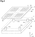
- FIG. 2 is a perspective view showing a portion of the semiconductor photodetection device shown in FIG. 1 .
- FIG. 3 is a plan view of a semiconductor substrate shown in FIG. 1 .
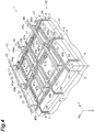
- FIG. 4 is a perspective view showing the semiconductor substrate shown in FIG. 1 .
- FIG. 5 is a diagram showing a sectional configuration of the semiconductor photodetection device shown in FIG. 1 .
- FIG. 6 is a plan view showing the semiconductor substrate shown in FIG. 1 .
- the semiconductor photodetection device 1 includes a glass substrate 2, a semiconductor substrate 3, a wiring layer 4, and a circuit board 5.
- the glass substrate 2, the semiconductor substrate 3, the wiring layer 4, and the circuit board 5 are disposed in that order in a Z-axis direction.
- the glass substrate 2, the semiconductor substrate 3, the wiring layer 4, and the circuit board 5 have rectangular shapes in plan view.
- the semiconductor photodetection device 1 is, for example, disposed such that light to be detected is incident on the glass substrate 2 and detects incident light, which is the light made incident.
- the glass substrate 2 is made of a transparent glass material that transmits light.
- the glass substrate 2 has a main surface 2A and a main surface 2B, which oppose each other, and side surfaces 2C.
- the main surface 2A and the main surface 2B are flat surfaces.
- the glass substrate 2 is adhered to the semiconductor substrate 3 by an optical adhesive OA.
- the optical adhesive OA is, for example, a resin having a light transmitting property.
- the glass substrate 2 may be formed directly on the semiconductor substrate 3.
- the glass substrate 2 has a function of holding the semiconductor substrate 3.
- the glass substrate 2 constitutes a holding member and the optical adhesive OA constitutes an adhesive layer.
- the semiconductor substrate 3 is made of Si (silicon), and is a p-type conductivity semiconductor substrate.
- the semiconductor substrate 3 has a main surface 3A and a main surface 3B, which oppose each other, and side surfaces 3C.
- the main surface 3A of the semiconductor substrate 3 and the main surface 2B of the glass substrate 2 oppose each other via the optical adhesive OA.
- the main surface 3A is a surface onto which light to the semiconductor substrate 3 is incident.. In the present embodiment, incident light is incident on the semiconductor substrate 3 upon transmission through the glass substrate 2.
- the main surface 3B is the first main surface
- the main surface 3A is the second main surface.
- the detailed configuration of the semiconductor substrate 3 will be described below.
- the wiring layer 4 is disposed between the semiconductor substrate 3 and the circuit board 5.
- the wiring layer 4 is provided at the main surface 3B of the semiconductor substrate 3.
- the wiring layer 4 has a function of electrically connecting the semiconductor substrate 3 and the circuit board 5. The detailed configuration of the wiring layer 4 will be described below.
- the circuit board 5 has a main surface 5A and a main surface 5B, which oppose each other, and side surfaces 5C.
- the main surface 5A of the circuit board 5 and the main surface 3B of the semiconductor substrate 3 oppose each other via the wiring layer 4.
- a side surface 2C of the glass substrate 2, a side surface 3C of the semiconductor substrate 3, and a side surface 5C of the circuit board 5 are flush with each other.
- respective outer edges of the glass substrate 2, the semiconductor substrate 3, and the circuit board 5 are matched to each other.
- the respective outer edges of the glass substrate 2, the semiconductor substrate 3, and the circuit board 5 do not have to be matched to each other.
- an area of the circuit board 5 may be larger than respective areas of the glass substrate 2 and the semiconductor substrate 3.
- the side surfaces 5C of the circuit board 5 are positioned further outward in an XY axis plane than the side surfaces 2C of the glass substrate 2 and the side surfaces 3C of the semiconductor substrate 3.
- the circuit board 5 constitutes, for example, an ASIC (Application Specific Integrated Circuit).
- a plane parallel to the respective main surfaces of the semiconductor substrate 3 and the circuit board 5 is the XY axis plane and a direction orthogonal to the respective main surfaces is the Z axis direction.
- the semiconductor substrate 3, the wiring layer 4, and the circuit board 5 of the semiconductor photodetection device 1 are shown schematically.
- illustration of the glass substrate 2 is omitted and an interior of the wiring layer 4 is shown.
- the semiconductor substrate 3 includes a plurality of cells U that are arrayed two-dimensionally in a matrix.
- the plurality of cells U are arrayed two-dimensionally in M rows and N columns.
- M and N are integers not less than 2.
- the number of the cells U is, for example, "1024 (32 rows ⁇ 32 columns)”.
- An interval W between mutually adjacent cells U is, for example, approximately 10 to 500 ⁇ m.
- Each of the plurality of cells U includes one or a plurality of avalanche photodiodes APD.
- APD avalanche photodiode
- the wiring layer 4 includes a plurality (four, in the present embodiment) of bump electrodes 41a to 41d.
- the bump electrodes 41a to 41d are provided at positions corresponding to corner portions of the semiconductor substrate 3 and corner portions of the circuit board 5 in the XY axis plane.
- one side surface among a pair of side surfaces opposing each other in the Z axis direction is connected to an electrode pad included in the wiring layer 4 and the other side surface is connected to an electrode pad provided on the main surface 5A of the circuit board 5.
- an overall length of the wiring layer 4 is greater than a length of each of the bump electrodes 41a to 41d.
- wires of the wiring layer 4 electrically connected to an anode of each avalanche photodiode APD are electrically connected via the bump electrode 41a to the circuit board 5.
- Wires of the wiring layer 4 electrically connected to a cathode of each avalanche photodiode APD are electrically connected via the bump electrode 41b to the circuit board 5.
- the bump electrode 41c and the bump electrode 41d are dummy bump electrodes and serve a role of preventing the semiconductor substrate 3 from becoming inclined with respect to the circuit board 5.
- each avalanche photodiode APD includes an n-type conductivity semiconductor region 31, and a p-type conductivity semiconductor region 32.
- the semiconductor region 31 and the semiconductor region 32 form a pn junction of the avalanche photodiode APD.
- Each avalanche photodiode APD includes a p-type conductivity semiconductor region 33.
- An impurity concentration of the semiconductor region 33 is higher than an impurity concentration of the semiconductor region 32.
- the bias voltage is not less than a breakdown voltage of each avalanche photodiode APD.
- each avalanche photodiode APD operates in a Geiger mode when the bias voltage is applied.
- the semiconductor region 31 is a first semiconductor region
- a semiconductor region constituted of the semiconductor region 32 and the semiconductor region 33 is a second semiconductor region.
- the semiconductor region 32 surrounds the semiconductor region 31 (side surfaces and bottom surface), and the semiconductor region 33 surrounds the semiconductor region 32 (side surfaces and bottom surface).
- the semiconductor region 33 includes a region 33a, opposing the semiconductor region 31 via the semiconductor region 32, and a region 33b, connected to the region 33a.
- the region 33b intersects with or is orthogonal to the region 33a when viewed in an X axis direction or a Y axis direction.
- the region 33b has a frame shape.
- the region 33b surrounds a semiconductor region constituted of the semiconductor region 31, the semiconductor region 32, and the region 33a.
- the region 33b has a rectangular frame shape when viewed in the Z axis direction.
- the semiconductor region 31, the semiconductor region 32, and the region 33b of the semiconductor region 33 form the main surface 3B of the semiconductor substrate 3.
- each of the semiconductor region 31, the semiconductor region 32, and the region 33b form a portion of the main surface 3B.
- the region 33a and the region 33b form the main surface 3A of the semiconductor substrate 3.
- the region 33a, the semiconductor region 32, and the semiconductor region 31 are disposed in that order from the optical adhesive OA (circuit board 5) in the Z axis direction.
- a peripheral edge of the semiconductor region 33 when viewed in the Z axis direction forms a peripheral edge of each avalanche photodiode APD (each cell U).
- a trench 34 is formed in the semiconductor substrate 3. Outer side surfaces in the X axis direction or the Y axis direction of the regions 33b of the semiconductor regions 33 form side surfaces of the trench 34.
- the trench 34 opens to the main surface 3A and the main surface 3B. In other words, the trench 34 penetrates through the semiconductor substrate 3 in a direction (the Z axis direction) in which the main surface 3A and the main surface 3B oppose each other.
- the Z axis direction is also a thickness direction of the semiconductor substrate 3.
- the trench 34 physically separates mutually adjacent cells U, among the plurality of cells U, from each other. Specifically, the trench 34 surrounds each of the plurality of cells U when viewed in a direction (the Z axis direction) orthogonal to the main surface 3A.
- the trench 34 is formed in a lattice in the semiconductor substrate 3 when viewed in the Z axis direction. In the present embodiment, the trench 34 is formed in a substantially square lattice in the semiconductor substrate 3 when viewed in the Z axis direction.
- the semiconductor photodetection device 1 includes a light-shielding member 6 and an insulating film 7.
- the light-shielding member 6 is provided in the trench 34 formed in the semiconductor substrate 3.
- the insulating film 7 covers the light-shielding member 6.
- the light-shielding member 6 is made of a material that reflects light.
- the light-shielding member 6 may instead be made of a material that absorbs light without reflecting it.
- the material included in the light-shielding member 6 is, for example, tungsten.
- the light-shielding member 6, covered by the insulating film 7, is disposed to fill the trench 34 and projects out toward the glass substrate 2 from the main surface 3A.
- the light-shielding member 6 includes a portion 6a, positioned inside the trench 34, and a portion 6b, projecting out from the main surface 3A of the semiconductor substrate 3.
- the portion 6b of the light-shielding member 6 is positioned inside the optical adhesive OA.
- the portion 6a of the light-shielding member 6 is positioned inside the trench 34 to surround each of the plurality of cells U when viewed in the Z axis direction.
- a length of the portion 6a of the light-shielding member 6 in the Z axis direction is substantially the same as a length of the trench 34 in the Z axis direction.
- the portion 6a of the light-shielding member 6 extends in the Z axis direction between an opening end at the main surface 3B and an opening end at the main surface 3A of the trench 34.
- positions in the Z axis direction of one end, among both ends in the Z axis direction of the light-shielding member 6, that is close to the main surface 3B and the main surface 3B are substantially the same as each other.
- the positions in the Z axis direction of the one end, among both ends in the Z axis direction of the light-shielding member 6, that is close to the main surface 3B and the main surface 3B may differ from each other. That is, a surface of the one end of the light-shielding member 6 and the main surface 3B do not have to be flush with each other.
- the portion 6a of the light-shielding member 6 opposes inner side surfaces of the trench 34 via the insulating film 7.
- the portion 6a of the light-shielding member 6 is positioned between outer surfaces of respective semiconductor regions 33 of mutually adjacent avalanche photodiodes APD in the X axis direction or the Y axis direction.
- the portion 6b constitutes the second portion.
- the light-shielding member 6 has a shape corresponding to the trench 34 when viewed in the Z axis direction.
- the light-shielding member 6 has a lattice shape when viewed in the Z axis direction.
- the light-shielding member 6 has a substantially square lattice shape when viewed in the Z axis direction.
- the insulating film 7 covers surfaces, other than the surface exposed from the main surface 3B, of the light-shielding member 6. Specifically, side surfaces of the portion 6a of the light-shielding member 6 and a surface of the portion 6b of the light-shielding member 6 are covered by the integrally-formed insulating film 7.
- the insulating film 7 includes a portion covering the side surfaces of the portion 6a of the light-shielding member 6 and a portion covering the surface of the portion 6b of the light-shielding member 6.
- the insulating film 7 (the portion covering the side surfaces of the portion 6a) is positioned between the light-shielding member 6 and the semiconductor region 33.
- Insulation between the semiconductor region 33 (the avalanche photodiodes APD) and the light-shielding member 6 is thereby secured.
- the portion of the insulating film 7 covering the surface of the portion 6b of the light-shielding member 6 is positioned inside the optical adhesive OA.
- the portion of the insulating film 7 covering the surface of the portion 6b of the light-shielding member 6 contacts the optical adhesive OA.
- the material including the insulating film 7 is selected, for example, in consideration of an insulating property between the semiconductor region 33 and the light-shielding member 6, a bonding property with the light-shielding member 6.
- the insulating film 7 is made, for example, of SiO 2 (silicon dioxide).
- each region (each avalanche photodiode APD) of the semiconductor substrate 3 surrounded by the trench 34 includes a first region positioned at an inner side and a second region positioned at an outer side of the first region to surround the first region.
- the first region is the semiconductor region constituted of the semiconductor region 31, the semiconductor region 32, and the region 33a of the semiconductor region 33.
- the second region is a semiconductor region constituted of the region 33b of the semiconductor region 33.
- the main surface 3A includes a tapered surface 33c that is inclined such that a length of the second region (region 33b) in the Z axis direction increases as a distance to the trench 34 decreases.
- the tapered surface 33c formed on the main surface 3A surrounds the first region when viewed in the Z axis direction.
- the region 33b of the semiconductor region 33 projects out toward the glass substrate 2 from a portion of the main surface 3A that is constituted of the region 33a of the semiconductor region 33.
- an edge of the tapered surface 33c close to the trench 34 forms the peripheral edge of each avalanche photodiode APD.
- the wiring layer 4 includes a wire 42, a wire 43, and an insulating layer 44.
- the wire 42 applies the bias voltage to the avalanche photodiode APD in each cell U.
- the wire 43 outputs the signal from the avalanche photodiode APD in each cell U. Illustration of the insulating layer 44 is omitted in FIG. 4 and FIG. 6 . In FIG. 5 , a sectional configuration of the insulating layer 44 is shown and hatching of the insulating layer 44 is omitted.
- mutually adjacent cells U are physically separated from each other by the trench 34 and are thus not electrically connected. Therefore, to make the avalanche photodiode APD included in each cell U operate, the wire 42 and the wire 43 are physically and electrically connected to each cell U.
- the wire 42 electrically connects the bump electrode 41a and each of the plurality of cells U.
- the circuit board 5 is electrically connected to the anode (semiconductor region 33) of the avalanche photodiode APD included in each cell U via the bump electrode 41a and the wire 42.
- the wire 43 electrically connects the bump electrode 41b and each of the plurality of cells U.
- the circuit board 5 is electrically connected to the cathode (semiconductor region 31) of the avalanche photodiode APD included in each cell U via the bump electrode 41b and the wire 43.
- the wire 42 and the wire 43 are provided on the main surface 3B of the semiconductor substrate 3. In the present embodiment, the wire 42 and the wire 43 oppose the main surface 3B via the insulating layer 44. For example, when the wire 42 constitutes a second wire, the wire 43 constitutes a first wire.
- the wire 42 includes a plurality of branch wires 45 and a common wire 46.
- the plurality of branch wires 45 are provided for a plurality of cell groups (referred to hereinafter as "column direction cell groups"), each including a plurality of cells U aligned in a column direction, and in correspondence with each column direction cell group.
- the plurality of branch wires 45 are respectively provided for each of N column direction cell groups that each include M cells U aligned in the column direction.
- the column direction is the Y axis direction and a row direction, to be described below, is the X axis direction.
- the plurality of column direction cell groups constitute N second cell groups.
- Each branch wire 45 includes a common wire 45a and a plurality of connection wires 45b.
- the common wire 45a of each branch wire 45 is disposed along the direction in which the plurality of cells U, included in the column direction cell group positioned at the corresponding column, are aligned.
- the plurality of common wires 45a are provided substantially in parallel to each other. In other words, the plurality of common wires 45a are aligned along the row direction in correspondence with the respective column direction cell groups.
- the plurality of connection wires 45b electrically connect each common wire 45a and the semiconductor regions 33 of the respective avalanche photodiodes APD included in the corresponding column direction cell group. When viewed in the X axis direction, the common wire 45a and each connection wire 45b intersect each other.
- the common wire 45a and the plurality of connection wires 45b are made of the same metal material and are made, for example, of aluminum.
- the common wire 45a and the plurality of connection wires 45b may be made of a metal material.
- the metal material includes Cu (copper), Ti (titanium), Ni (nickel), Au (gold), or Pt (platinum).
- the plurality of branch wires 45 constitute a plurality of second branch wires.
- Each of the plurality of branch wires 45 is connected to the common wire 46.
- the common wire 45a of each of the plurality of branch wires 45 is electrically connected to the common wire 46.
- the common wire 46 intersects each common wire 45a when viewed in the Z axis direction.
- the common wire 46 is disposed, for example, in a region outside an incidence region, which, in the semiconductor substrate 3, is formed to include all of the plurality of cells U.
- the incidence region indicates, for example, a range in the semiconductor photodetection device 1 in which the light to be detected is incident.
- the common wire 46 is electrically connected to the bump electrode 41a.
- the common wire 46 is made of the same metal material as the plurality of branch wires 45.
- the wire 43 includes a plurality of branch wires 47 and a common wire 48.
- the plurality of branch wires 47 are provided for a plurality of cell groups (referred to hereinafter as "row direction cell groups"), each including a plurality of cells U aligned in a row direction, and in correspondence with each row direction cell group.
- the plurality of branch wires 47 are respectively provided for each of M row direction cell groups that each include N cells U aligned in the row direction.
- the plurality of row direction cell groups constitute M first cell groups.
- Each branch wire 47 includes a common wire 47a, a plurality of quenching resistors 47b, and a plurality of connection wires 47c.
- the common wire 47a of each branch wire 47 is disposed along the direction in which the plurality of cells U, included in the row direction cell group positioned at the corresponding row, are aligned.
- the plurality of common wires 47a are provided substantially in parallel to each other. In other words, the plurality of common wires 47a are aligned along the column direction in correspondence with each row direction cell group.
- the plurality of common wires 47a intersect the plurality of common wires 45a when viewed in the Z axis direction.
- Each of the plurality of common wires 47a is electrically connected to the semiconductor regions 31 of the respective avalanche photodiodes APD included in the row direction cell groups corresponding to each common wire 47a via the quenching resistors 47b and the connection wires 47c.
- the common wire 47a and each connection wire 47c intersect each other.
- the common wire 47a and the connection wire 47c are made of the same metal material and are made, for example, of aluminum.
- the common wire 47a and the connection wire 47c may be made of a metal material.
- the metal material includes Cu (copper), Ti (titanium), Ni (nickel), Au (gold), or Pt (platinum).
- the quenching resistor 47b When viewed in the Z axis direction, the quenching resistor 47b is disposed to be oriented along peripheral edge of the semiconductor region 31.
- the quenching resistors 47b are made of a material of higher resistance value than the material forming the common wires 47a and the connection wires 47c and are made, for example, of SiCr (silicon chromium).
- the quenching resistors 47b may be made of polysilicon, NiCr (nickel chromium), or FeCr (ferrochrome).
- the plurality of branch wires 47 constitute a plurality of first branch wires.
- Each of the plurality of branch wires 47 is connected to the common wire 48.
- the common wire 47a of each of the plurality of branch wires 47 is electrically connected to the common wire 48.
- the common wire 48 intersects each common wire 47a when viewed in the Z axis direction.
- the common wire 48 and the common wire 46 of the wire 42 are disposed to intersect mutually when viewed in the Z axis direction.
- the common wire 48 is disposed, for example, in a region outside the incidence region in the semiconductor substrate 3.
- the common wire 48 is electrically connected to the bump electrode 41b.
- the common wire 48 is made of the same metal material as the common wires 47a and the connection wires 47c.
- the positions in the Z axis direction of the common wires 45a of the wire 42, the common wires 47a of the wire 43, and quenching resistors 47b of the wire 43 differ from each other.
- the common wires 47a, the quenching resistors 47b, and the common wires 45a are disposed in that order from the main surface 3B of the semiconductor substrate 3.
- Cross-sectional shapes of the common wires 45a, the common wires 47a, and the quenching resistors 47b in a plane orthogonal to the X axis direction or the Y axis direction are, for example, rectangular.
- Cross-sectional shapes of the connection wires 45b of the wire 42 and the connection wires 47c of the wire 43 in a plane orthogonal to the Z axis direction are, for example, rectangular.
- a thickness (length in the Z axis direction) of the common wire 45a is approximately 600 nm
- a thickness of the common wire 47a is approximately 600 nm
- a thickness of the quenching resistor 47b is approximately 5 nm.
- a clearance in the Z axis direction between the common wire 45a and the quenching resistor 47b is approximately 300 nm
- a clearance in the Z axis direction between the common wire 47a and the quenching resistor 47b is approximately 300 nm.
- a clearance between the common wire 47a and the main surface 3B of the semiconductor substrate 3 is approximately 300 nm.
- the insulating layer 44 covers the wire 42 and the wire 43.
- the insulating layer 44 is made of a material capable of securing insulation between the wire 42 and the wire 43 that are connected to mutually different potentials and is made, for example, of SiO 2 (silicon oxide). As an example, a thickness of the insulating layer 44 is approximately 2.5 ⁇ m.
- the insulating layer 44 may cover entireties of the wire 42 and the wire 43 with the exception of connection portions to the semiconductor substrate 3 and the circuit board 5.
- the insulating layer 44 may cover a portion of the wire 42 and a portion of the wire 43. In this case, the insulating layer 44 may cover the branch wires 45 of the wire 42 and the branch wires 47 of the wire 43.
- each avalanche photodiode APD forms a light receiving region.
- the light receiving region is formed of the semiconductor region 31 and the semiconductor region 32.
- a contact resistance between the avalanche photodiode APD and the wire 42 is reduced by the wire 42 being electrically connected to the semiconductor region 32 via the semiconductor region 33 of higher impurity concentration than the semiconductor region 32.
- the wire 42 (connection wire 45b) is electrically connected to one corner portion 33d of the semiconductor region 33 (see FIG. 6 ).
- the peripheral edge of the semiconductor region 31 includes a curved portion 31a at a position corresponding to the corner portion 33d.
- the curved portion 31a is formed to project out toward a center of each avalanche photodiode APD when viewed in the Z axis direction.
- a distance ⁇ between a portion of the corner portion 33d that is a connection portion with the connection wire 45b and the semiconductor region 31 (curved portion 31a) is greater than a distance ⁇ between the trench 34 and the semiconductor region 31.
- the distance ⁇ is the shortest distance between the connection portion, of the connection wire 45b and the semiconductor region 33, and the semiconductor region 31 when viewed in the Z axis direction.
- the distance ⁇ is the shortest distance between the trench 34 and the semiconductor region 31 when viewed in the Z axis direction.
- the bias voltage (reverse bias voltage) is applied all at once to the avalanche photodiodes APD respectively included in the plurality of cells U via the wire 42.
- incident light photon
- photoelectric conversion is performed in an interior of the semiconductor substrate 3 and a photoelectron is generated.
- Avalanche multiplication is performed at a pn junction interface of the avalanche photodiode APD and the multiplied electron group flows into the circuit board 5 via the wire 43.
- a signal (current signal) accompanying the incidence of light is output from the avalanche photodiode APD to the circuit board 5.
- the signal corresponding to the incident light is output to the circuit board 5.
- an incident light amount of the light is measured in accordance with the signal output from the avalanche photodiodes APD in the cells U.
- FIGS. 7(a) to 7(c) and FIGS. 8(a) to 8(c) are diagrams showing the manufacturing process of the semiconductor photodetection device shown in FIG. 1 .
- FIG. 9 is a diagram showing an etching process. In these drawings, cross-sectional shapes of the respective elements are shown and hatching is omitted.
- the manufacturing process of the semiconductor photodetection device 1 shown in FIGS. 7(a) to 7(c) and FIGS. 8(a) to 8(c) includes a temporary bonding step, a polishing step, an etching step, a coating step, a main bonding step, and a peeling step.
- the temporary bonding step, the polishing step, the etching step, the coating step, the main bonding step, and the peeling step are performed in that order.
- an Si (silicon) substrate 8 that is to be a base material of the semiconductor substrate 3 is prepared.
- a trench 34a is formed to surround regions in which the respective cells U (the respective avalanche photodiodes APD) are to be formed.
- the main surface of the Si substrate 8 in which the trench 34a is formed corresponds to the main surface 3B of the semiconductor substrate 3 and hereinafter, this main surface of the Si substrate 8 will also be referred to as the "main surface 3B".
- the Si substrate 8 is a substrate that is thicker than the semiconductor substrate 3 included in the semiconductor photodetection device 1 that is manufactured.
- a depth (length) of the trench 34a is longer than the length of the trench 34 formed in the semiconductor substrate 3.
- An area of the trench 34a when viewed in a direction orthogonal to the main surface 3B is the same as an area of the trench 34.
- the respective semiconductor regions constituting the respective avalanche photodiodes APD are formed, for example, by doping the Si substrate 8, in which the trench 34a is formed, with a p-type impurity and an n-type impurity.
- a Group 13 element for example, B
- a Group 15 element for example, P or As
- the trench 34a may be formed after the respective semiconductor regions constituting the respective avalanche photodiodes APD are formed in the Si substrate 8.
- the light-shielding member 6 covered by the insulating film 7 is formed inside the trench 34a.
- an interior of a region demarcated by a virtual surface that is flush with the main surface 3B and the trench 34a is filled with the light-shielding member 6 and the insulating film 7.
- the light-shielding member 6 that is covered by the insulating film 7 is disposed inside the trench 34a such that one side surface of the light-shielding member 6 that is not covered by the insulating film 7 is exposed from the main surface 3B.
- a temporary holding substrate 9 is then prepared and the temporary holding substrate 9 is adhered onto the main surface 3B of the Si substrate by an adhesive AD that changes in tack strength with temperature.
- the temporary holding substrate 9 is used in the manufacturing process of the semiconductor photodetection device 1.
- the temporary holding substrate 9 is, for example, a glass substrate.
- the adhesive AD has an adhesive strength that maintains an adhered state of the temporary holding substrate 9 and the Si substrate 8 at ordinary temperature, and the adhered state of the Si substrate 8 and the temporary holding substrate 9 is released by the adhesive AD being heated.
- the adhesive AD may have an adhesive strength that maintains the adhered state of the temporary holding substrate 9 and the Si substrate 8 regardless of temperature. In this case, the adhered state of the Si substrate 8 and the temporary holding substrate 9 may be released by irradiating the adhesive AD with light (for example, laser light).
- a main surface of the Si substrate 8 opposite the main surface 3B is polished.
- the Si substrate 8 is polished such that a thickness of the Si substrate 8 becomes a length obtained by adding a predetermined distance to the depth of the trench 34a.
- the thickness of the polished Si substrate 8 is approximately half the thickness of the Si substrate 8 prepared in the temporary bonding step.
- the main surface of the Si substrate 8 opposite the main surface 3B is etched to make the thickness of the Si substrate 8 even thinner and form the main surface 3A of the semiconductor substrate 3.
- the main surface of the Si substrate 8 opposite the main surface 3B is eroded by an etching liquid (etchant) such that the thickness of the Si substrate becomes smaller than the depth of the trench 34a.
- a thickness of the semiconductor substrate 3 (length between the main surface 3A and the main surface 3B) is defined by the thickness of the etched Si substrate 8, a portion of the trench 34a becomes non-existent, and the trench 34 having the same length as that between the main surface 3A and the main surface 3B is formed.
- FIG. 9(a) to FIG. 9(c) The process in which the main surface 3A is formed by the etching step is shown in FIG. 9(a) to FIG. 9(c) .
- FIG. 9(a) to FIG. 9(c) illustration of the temporary holding substrate 9 is omitted.
- An intermediate shown in FIG. 9(a) is the intermediate after polishing of the Si substrate 8 that is shown in FIG. 7(b) and this intermediate is immersed in a caustic agent or other etching liquid. After immersion in the etching liquid, etching progresses at substantially the same rate across an entirety of the main surface of the Si substrate 8 opposite the main surface 3B.
- the thickness of the Si substrate 8 changes substantially uniformly until the thickness of the Si substrate 8 becomes substantially the same as the depth of the trench 34 (total value of the length of the light-shielding member 6 and the thickness of the insulating film 7) as shown in FIG. 9(b) .
- the insulating film 7 covering the light-shielding member 6 is exposed to the etching liquid and even if etching progresses from this state, the insulating film 7 is not etched (eroded). In other words, the light-shielding member 6 and the insulating film 7 are maintained in the prepared shapes.
- plane orientations in which the Si substrate 8 is etched differ from that in the state shown in FIG. 9(b) and etching progresses in the different plane orientations. Specifically, etching progresses at a plane orientation, in which etching progresses in a thickness direction of the Si substrate 8, and plane orientations, in which etching progresses toward a center of the light-shielding member 6 (trench 34a) covered by the insulating film 7. With the plane orientations directed toward the center of the light-shielding member 6, the rate (etching rate) at which etching progresses is slow in comparison to that of the other plane orientation.
- the main surface 3A of the semiconductor substrate 3 formed at the point of end of etching includes the tapered surface 33c (see FIG. 7(c) ).
- the optical adhesive OA is coated onto the main surface 3A of the semiconductor substrate 3.
- the optical adhesive OA is coated to cover an entirety of the surface of the insulating film 7 projecting out from the trench 34.
- the main bonding step in which the glass substrate 2 is adhered onto the main surface 3A of the semiconductor substrate 3 via the optical adhesive OA, is performed as shown in FIG. 8(b) .
- the glass substrate 2 that is adhered in the main bonding step is a member that is included even after manufacture of the semiconductor photodetection device 1.
- the optical adhesive OA differs from the adhesive AD used in the temporary bonding step.
- the temporary holding substrate 9 is peeled from the main surface 3B of the semiconductor substrate 3.
- the temporary holding substrate 9 and the adhesive AD are removed by a machine or a worker after the adhesive AD is heated.
- the trench 34 is thus formed in the semiconductor substrate 3 and the light-shielding member 6 and the insulating film 7 are disposed in the trench 34.
- an avalanche photodiode APD may generate a secondary light different from the incident light.
- the avalanche photodiode APD included in the adjacent cell U may perform avalanche multiplication of a carrier generated by the incident secondary light.
- the trench 34 surrounding each of the plurality of avalanche photodiodes APD when viewed in the Z axis direction, is formed in the semiconductor substrate 3, and the light-shielding member 6, including the portion 6a, positioned inside the trench 34, and the portion 6b, projecting out from main surface 3A, is included.
- a configuration where the light-shielding member 6 includes the portion 6b projecting out from a main surface, prevents secondary light from being incident on an avalanche photodiode APD in an adjacent cell U even more reliably in comparison to a configuration where a light-shielding member does not include a portion that projects out.
- the light-shielding member 6 thus reduces optical crosstalk reliably.
- the portion 6b of the light-shielding member 6 is less likely to be protected by the semiconductor substrate 3 than the portion 6a of the light-shielding member 6 that is positioned inside the semiconductor substrate 3 (trench 34).
- the portion 6b may thus be exposed to an atmospheric environment outside the semiconductor substrate 3.
- the light-shielding member 6, including the portion 6b may corrode. If the light-shielding member 6 corrodes, the light-shielding member 6 is unlikely to reduce optical crosstalk.
- the insulating film 7 includes a portion that covers the surface of the portion 6b of the light-shielding member 6 that projects out from the main surface 3A of the semiconductor substrate 3. Even if the portion 6b of the light-shielding member 6 projects out from the main surface 3A, it is unlikely to be exposed to the atmospheric environment outside the semiconductor substrate 3. The light-shielding member 6 is thus unlikely to corrode and the light-shielding member 6 reduces optical crosstalk reliably.
- the light-shielding member 6 is made of a material that reflects light.
- light which, among the light incident on the semiconductor photodetection device 1, is incident toward the light-shielding member 6, is reflected by the light-shielding member 6.
- a portion of the light that is incident toward the light-shielding member 6 may thus be reflected toward the pn junction formed in an avalanche photodiode APD. Therefore, with the present configuration, an amount of photoelectrons generated in the avalanche photodiodes APD may increase in comparison to a case where the light-shielding member 6 is made of a material that absorbs light. Consequently, detection sensitivity of the incident light at the semiconductor photodetection device 1 may be improved.
- the main surface 3A includes the tapered surface 33c.
- a portion of light which, among the light incident on the semiconductor photodetection device 1, is directed toward the tapered surface 33c, may be reflected by the tapered surface 33c toward the pn junction of an avalanche photodiode APD. Therefore, with the present configuration, the amount of photoelectrons generated in the avalanche photodiodes APD may increase in comparison to a case where an entire surface of the main surface 3A in each avalanche photodiode APD is flat. Consequently, the detection sensitivity of the incident light at the semiconductor photodetection device 1 may be improved.
- the insulating film 7 includes a portion that contacts the side surfaces of the trench 34 and covers the portion 6a of the light-shielding member 6.
- the portion covering the portion 6b and the portion covering the portion 6a are formed integrally.
- the portion of the insulating film 7 covering the portion 6a secures electrical insulation between the semiconductor substrate 3 and the light-shielding member 6.
- the light-shielding member 6 is covered reliably and durability of the light-shielding member 6 is improved because the portion covering the portion 6a and the portion covering the portion 6b are formed integrally. Therefore with the present configuration, optical crosstalk is reduced even more reliably in comparison to a configuration where the portion covering the portion 6a and the portion covering the portion 6b are formed as separate bodies.
- the portion 6b of the light-shielding member 6 and the portion of the insulating film 7 covering the portion 6b are positioned inside the optical adhesive OA.
- the portion 6b of the light-shielding member 6 projecting out from the main surface 3A of the semiconductor substrate 3 is held by the optical adhesive OA and a force of holding the light-shielding member 6 is thus improved, for example, in comparison to a case where the portion of the insulating film 7 covering the portion 6b is exposed to the exterior of the semiconductor substrate 3.
- the plurality of branch wires 45 are respectively provided for each column direction cell group and the plurality of branch wires 47 are respectively provided for each row direction cell group. Therefore, in a case where each of the plurality of avalanche photodiodes APD is to be connected to common potentials via each of the wire 42 and the wire 43, the present configuration simplifies the wires 42 and 43 electrically connected to the avalanche photodiode APD included in each cell U in comparison to a case where a single wire is provided for each cell U.
- Each branch wire 45 (connection wires 45b) is connected to the semiconductor regions 33 of the avalanche photodiodes APD included in the corresponding cells U among the plurality of cells U.
- the shortest distance between the connection portion, of the connection wire 45b and the semiconductor region 33, and the semiconductor region 31 is greater than the shortest distance between the semiconductor region 31 and the trench 34.
- a configuration as in the semiconductor photodetection device described in Patent Document 1 mentioned above may be considered.
- a wire hereinafter referred to as the "anode wire” applying a bias voltage is disposed on one main surface of a semiconductor substrate and a wire (hereinafter referred to as the "cathode wire") outputting a signal is disposed on another main surface of the semiconductor substrate.
- a bias voltage that is not less than the breakdown voltage must be applied and thus a comparatively high voltage is applied to the avalanche photodiode via the anode wire.
- the anode wire does not need to be physically connected to each cell and therefore a degree of freedom of configuration of the anode wire increases. It therefore becomes possible to arrange the wires such as to secure a distance between a connection portion (for example, a portion of a semiconductor region of p-type conductivity) of the avalanche photodiode at which the anode wire is connected and a semiconductor region (for example, a semiconductor region of n-type conductivity) at which the cathode wire is electrically connected and prevent occurrence of dielectric breakdown therebetween.
- a connection portion for example, a portion of a semiconductor region of p-type conductivity
- a semiconductor region for example, a semiconductor region of n-type conductivity
- a region of one cell is small and therefore if the anode wire and the cathode wire are disposed on one main surface, there is concern for occurrence of the abovementioned dielectric breakdown. Therefore generally, the anode wire and the cathode wire are respectively disposed at different main surfaces as described in Patent Document 1.
- both the wire 42, applying the bias voltage to the avalanche photodiode APD in the respective cells U, and the wire 43, outputting the signals from the avalanche photodiode APD in the respective cells U, are provided on the main surface 3B, which is one of the main surfaces of the semiconductor substrate 3.
- the semiconductor photodetection device 1 is made a configuration that is suitable for practical use.
- the semiconductor substrate 3 and the circuit board 5 are electrically connected by providing electrodes or wires (for example, bump electrodes) for connection with the circuit board 5 on the one main surface of the semiconductor substrate 3.
- electrodes or wires for example, bump electrodes
- FIG. 10 is a plan view showing the semiconductor photodetection device according to the second embodiment.
- the semiconductor photodetection device 60 shown in FIG. 10 differs from the semiconductor photodetection device 1 shown in FIG. 1 in the point of including a semiconductor substrate 61 in place of the semiconductor substrate 3 and in the point of including wires 62 and 63 in place of the wires 42 and 43.
- illustration of an insulating layer covering each of the wire 62 and the wire 63 is omitted.
- the semiconductor substrate 61 includes a plurality of cells U that are arrayed two-dimensionally in M rows and N columns. As shown in FIG. 10 , each of the plurality of cells U includes one avalanche photodiode APD. Each of the plurality of cells U may include a plurality of avalanche photodiodes APD.
- the semiconductor substrate 61 has a main surface 61B and a main surface opposing the main surface 61B.
- the avalanche photodiode APD of each of the plurality of cells U includes an n-type conductivity semiconductor region 64, and a p-type conductivity semiconductor region 65. Although unillustrated, in a sectional configuration of the semiconductor substrate 61, the semiconductor region 65 surrounds the semiconductor region 64.
- each avalanche photodiode APD the semiconductor region 64 and the semiconductor region 65 form the main surface 61B of the semiconductor substrate 61.
- the trench 34 is formed to surround the respective cells U (the respective avalanche photodiodes APD) when viewed in the Z axis direction.
- the light-shielding member 6, covered by the insulating film 7, is provided inside the trench 34.
- illustration of the light-shielding member 6 and the insulating film 7 is omitted.
- the light-shielding member 6, covered by the insulating film 7, projects out from the main surface opposing the main surface 61B.
- the surface of the portion of the light-shielding member 6 projecting out from the main surface opposing the main surface 61B is covered by the insulating film 7.
- the semiconductor region 64 constitutes the first semiconductor region
- the semiconductor region 65 constitutes the second semiconductor region.
- the wire 62 includes a plurality of branch wires 66 and a common wire 67.
- the wire 63 includes a plurality of branch wires 68 and a common wire 69.
- a single branch wire 68 among the plurality of branch wires 68 is shown.
- Each of the plurality of branch wires 66 and each of the plurality of branch wires 68 are disposed alternately in the Y axis direction.
- the plurality of branch wires 66 are respectively provided for every two mutually adjacent row direction cell groups
- the plurality of branch wires 68 are respectively provided for every two mutually adjacent row direction cell groups.
- the two row direction cell groups with which each branch wire 66 corresponds is shifted by one row with respect to the two row direction cell groups with which each branch wire 68 corresponds.
- the respective branch wires 68 are respectively provided for every row direction groups of the (2 ⁇ m-1)th row and the (2 ⁇ m)th row, and the respective branch wires 66 are respectively provided for every row direction groups of the (2 ⁇ m)th row and the (2 ⁇ m+1)th row.
- m is an integer not less than 1.
- the respective branch wires 68 may be respectively provided for every row direction groups of the (2 ⁇ m)th row and the (2 ⁇ m+1)th row, and the respective branch wires 66 may be respectively provided for with every row direction groups of the (2 ⁇ m-1)th row and (2 ⁇ m)th row.
- the wire 63 constitutes the first wire.
- the branch wires 66 constitute the second branch wires
- the branch wires 68 constitute the first branch wires.
- Each branch wire 66 includes a common wire 66a and a plurality of connection wires 66b.
- the common wire 66a of each branch wire 66 is disposed between the corresponding two row direction cell groups (above the trench 34) when viewed in the Z axis direction.
- the plurality of connection wires 66b of each branch wire 66 electrically connect the semiconductor regions 65 of the avalanche photodiodes APD, included in the two row direction cell groups corresponding to the branch wire 66, and the common wire 66a.
- the bias voltage is applied to the avalanche photodiodes APD in the (2 ⁇ N) cells U included in two mutually adjacent row direction cell groups via one branch wire 66.
- the branch wire 66 (common wire 66a and connection wires 66b) is made, for example, of the same metal material as the common wire 45a.
- Each of the plurality of branch wires 66 is electrically connected to the common wire 67.
- a wire that is electrically connected to the row direction cell group of just the first row may be connected to the common wire 67.
- a wire that is electrically connected to the row direction cell group of just the M-th row may be connected to the common wire 67.
- the common wire 67 is electrically connected to the bump electrode 41a.
- the common wire 67 is, for example, made of the same metal material as the common wire 46.
- Each branch wire 68 includes a common wire 68a, a plurality of quenching resistors 68b, and a plurality of connection wires 68c.
- the common wire 68a of each branch wire 68 is disposed between the corresponding two row direction cell groups (above the trench 34) when viewed in the Z axis direction.
- the quenching resistor 68b of each branch wire 68 is electrically connected to the common wire 68a and is disposed along a peripheral edge of the semiconductor region 64.
- the connection wire 68c electrically connects the quenching resistor 68b and the semiconductor region 64 of the avalanche photodiode APD.
- the common wire 68a is electrically connected to the semiconductor region 64 of the avalanche photodiode APD via the quenching resistor 68b and the connection wire 68c.
- signals from the avalanche photodiodes APD included in two mutually adjacent row direction cell groups are output via one branch wire 68.
- the common wire 68a and the connection wires 68c are made, for example, of the same metal material as the common wire 47a.
- the quenching resistors 68b are made, for example, of the same material as the quenching resistors 47b.
- Each of the plurality of branch wires 68 is electrically connected to the common wire 69.
- the common wire 69 is electrically connected to the bump electrode 41b.
- a wire that is electrically connected to the row direction cell group of just the first row may be connected to the common wire 69.
- a wire that is electrically connected to the row direction cell group of just the M-th row may be connected to the common wire 69.
- the common wires 66a and the common wires 68a are disposed substantially parallel to each other.
- each common wire 66a and the common wire 67 intersect each other and each common wire 68a and the common wire 69 intersect each other.
- the common wire 67 and the common wire 69 are disposed substantially parallel to each other.
- positions in the Z axis direction of the common wires 66a and the common wires 68a are substantially the same as each other.
- Each semiconductor region 65 has a rectangular frame shape when viewed in the Z axis direction.
- the connection wire 66b is connected in a corner portion 65a of the semiconductor region 65.
- a peripheral edge of each semiconductor region 64 includes an inclined portion 64a that is inclined with respect to the X axis direction and the Y axis direction when viewed in the Z axis direction.
- a distance ⁇ 1 between a connection portion of the connection wire 66b in the corner portion 65a and the semiconductor region 64 (inclined portion 64a) may be greater than a distance ⁇ 1 between the trench 34 and the semiconductor region 64.
- the distance ⁇ 1 is the shortest distance between the connection portion, of the connection wire 66b and the semiconductor region 65, and the semiconductor region 64 when viewed in the Z axis direction.
- the distance ⁇ 1 is the shortest distance between the trench 34 and the semiconductor region 64 when viewed in the Z axis direction.
- the light-shielding member 6 is unlikely to corrode and the light-shielding member 6 reduces optical crosstalk reliably in the semiconductor photodetection device 60 as well.
- the branch wires 66 and the branch wires 68 are provided alternately according to each row. Therefore, for example, in a case where each of the plurality of cells U is to be connected to common potentials via each of the wire 62 and the wire 63, the number of wires on the main surface 61B is lessened in comparison to a case where wires are provided individually for each cell U.
- the present configuration thus simplifies the configuration of the wire 62 and the wire 63 electrically connected to the avalanche photodiode APD included in each cell U.
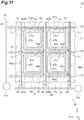
- FIG. 11 is a plan view showing the semiconductor photodetection device according to the third embodiment.
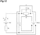
- FIG. 12 is a diagram showing an equivalent circuit of an avalanche photodiode.
- FIG. 13 is a diagram showing an example of a signal output from the avalanche photodiode.
- a semiconductor substrate 71 has an semiconductor region 72 of n-type conductivity and a semiconductor region 73 of p-type conductivity.
- the semiconductor substrate 71 is formed in the same manner as the semiconductor substrate 61 with the exception that a peripheral edge of the semiconductor region 72 does not include an inclined portion and detailed description of the respective semiconductor regions will thus be omitted.
- the trench 34 is formed to surround the respective cells U (the respective avalanche photodiodes APD) when viewed in the Z axis direction.
- the light-shielding member 6, covered by the insulating film 7, is provided inside the trench 34. In FIG. 11 , illustration of the light-shielding member 6 and the insulating film 7 is omitted.
- the light-shielding member 6, covered by the insulating film 7, projects out from the main surface opposing a main surface 71B.
- the surface of the portion of the light-shielding member 6 projecting out from the main surface opposing the main surface 71B is covered by the insulating film 7.
- the semiconductor region 72 constitutes the first semiconductor region
- the semiconductor region 73 constitutes the second semiconductor region.
- a capacitance increasing portion 74 is electrically connected to each common wire 47a. With the exception of a connection portion with the common wire 47a, the capacitance increasing portion 74 is positioned at an inner side of the quenching resistor 47b when viewed in the Z axis direction. A portion of the capacitance increasing portion 74 positioned at the inner side of the quenching resistor 47b is in a plate shape spreading in the XY axis plane and has a rectangular shape when viewed in the Z axis direction. The capacitance increasing portion 74 opposes the semiconductor region 72 of the avalanche photodiode APD.
- a size (area) of the capacitance increasing portion 74 is smaller than the semiconductor region 72, and the capacitance increasing portion 74 has, for example, an area of not less than half the semiconductor region 72.
- the capacitance increasing portion 74 is made, for example, of a metal material.
- the capacitance increasing portion 74 is made, for example, of aluminum.
- the metal material forming the capacitance increasing portion 74 may include Cu (copper), Ti (titanium), Ni (nickel), Au (gold), or Pt (platinum).
- a voltage Vbr indicates the breakdown voltage of the avalanche photodiode APD.
- a voltage Vbias indicates the voltage (bias voltage) applied to the avalanche photodiode APD.
- a resistor Rq indicates the quenching resistor.
- a resistor Rd indicates a serial resistance component that the semiconductor region of the avalanche photodiode APD has.
- a capacitor Cj indicates a static capacitance component that the semiconductor region of the avalanche photodiode APD has.
- a capacitor Cq indicates an effective static capacitance component present between the quenching resistor and the avalanche photodiode APD.
- a signal (current i1) which is in accordance with high frequency components of photoelectrons (carriers) generated by incidence of incident light on the avalanche photodiode APD in the state where the bias voltage is applied, is output not via the resistor Rq (quenching resistor) but via the capacitor Cq.
- a time constant which indicates a response speed of a signal (current i2) output via the resistor Rq, is large in comparison to the signal in accordance with the high frequency components that is output via the capacitor Cq.
- the waveform of the signal from the avalanche photodiode APD that is in accordance with the incident light is indicated as a change with time of a voltage value.
- the light-shielding member 6 is unlikely to corrode and the light-shielding member 6 reduces optical crosstalk reliably in the semiconductor photodetection device 70 as well.
- the main surface 3B, on which the wires 42 and 43 are provided may be the light incidence surface.
- a holding substrate that holds the semiconductor substrate 3 in place of the glass substrate 2 and the circuit board 5 may be provided.
- the semiconductor substrate 3 may be provided on the holding substrate such that the main surface 3A is opposed on the holding substrate.
- the holding substrate may be made of a material that does not transmit light.
- the wiring layer 4 does not have to include the insulating layer 44.
- the insulating layer 44 may be made of a material that transmits light.
- the bias voltage may be applied individually to each of the plurality of cells U.
- the bias voltage may be applied, according to each cell U, to the avalanche photodiode APD included in the cell U.
- the bias voltage may be applied to just specific cells U among the plurality of cells U arrayed in a matrix.
- a wire that applies the bias voltage may be provided individually for each of the plurality of cells U.
- the wire 42 or 62 does not have to include the common wire 46 or 67.
- the bias voltage may be applied, according to every single column direction cell group or every two row direction cell groups via the respective branch wires 45 or 66, to the cells U included in the cell group or groups. For example, in a case where the bias voltage is applied according to every single column direction group via the wire 42, the bias voltage may be applied at timings that differ according to each cell group.
- the output from each of the plurality of cells U may be output individually to the circuit board 5.
- the output of the avalanche photodiode APD included in each cell U may be read according to each cell U.
- layout positions of the respective avalanche photodiodes APD and the outputs from the avalanche photodiodes APD may be associated with each other in the circuit board 5.
- a wire that reads out the signal may be provided individually for each of the plurality of cells U.
- the wire 43 or 63 does not have to include the common wire 48 or 69.
- the signal may be read out, according to every single or two row direction cell group or groups via the respective branch wires 47 or 68, from the cells U included in the cell group or groups.
- the layer structure of the avalanche photodiode APD is not restricted thereto.
- the conductivity type of the semiconductor region 31 may be p-type and the conductivity type of the semiconductor region 32 and the semiconductor region 33 may be n-type.
- the conductivity type of the semiconductor region 64 or 72 may be p-type and the conductivity type of the semiconductor region 65 or 73 may be n-type.
- the semiconductor region 31, 64, or 72 may be constituted of a plurality of semiconductor regions differing mutually in impurity concentration.
- a wire applying the bias voltage may be electrically connected to the semiconductor region 31, 64, or 72, and a wire reading out the signal from the avalanche photodiode APD may be electrically connected to the semiconductor region 32, 33, 65, or 73.
- the portion covering the portion 6a of the light-shielding member 6 and the portion covering the portion 6b of the light-shielding member 6 may be formed as separate bodies.
- the portion covering the portion 6a of the light-shielding member 6 and the portion covering the portion 6b of the light-shielding member 6 are formed integrally, optical crosstalk is reduced even more reliably as mentioned above.
- the insulating film 7 does not to have to cover the light-shielding member 6 directly. In other words, the insulating film 7 may cover the light-shielding member 6 indirectly. For example, another layer may be provided between the insulating film 7 and the light-shielding member 6.
- the light-shielding member 6 may be made of a material not having conductivity. If the light-shielding member 6 is made of a material not having conductivity, the insulating film 7 does not have to cover the portion 6a of the light-shielding member 6. In this case, the insulating film 7 may cover just the portion 6b. For example, the insulating film 7 may cover an entire surface of the light-shielding member 6. In other words, the one end of the light-shielding member 6 in the Z axis direction does not have to be exposed from the semiconductor substrate 3.
- each of the plurality of cells U includes a plurality of avalanche photodiodes APD
- the plurality of avalanche photodiodes APD included in the cell U may be arrayed in a matrix.
- the cathodes and the anodes of the plurality of avalanche photodiodes APD included in the cell U may respectively be electrically connected mutually.
- an electrode connected to a wire electrically connecting and applying the bias voltage to each of the plurality of avalanche photodiodes APD included in the cell U or connected to a wire electrically connecting and reading out the signals from each of the plurality of avalanche photodiodes APD included in the cell U may be provided.
- connection portion of the branch wire 45 (connection wire 45b) and the semiconductor region 31 may be substantially equivalent to the distance ⁇ between the trench 34 and the semiconductor region 31.
- the distance ⁇ is greater than the distance ⁇ , the withstand voltage between the branch wire 45 and the semiconductor region 31 is improved.
- the light-shielding member 6 may be made of a material that absorbs light. On the other hand, when the light-shielding member 6 is made of a material that reflects light, the detection sensitivity of the incident light at the semiconductor photodetection device 1 may be improved as mentioned above.
- the main surface 3A does not have to include the tapered surface 33c. That is, the entirety of the main surface 3A may be substantially flat.
- the detection sensitivity of the incident light at the semiconductor photodetection device 1 may be improved as mentioned above.
Landscapes
- Engineering & Computer Science (AREA)
- Physics & Mathematics (AREA)
- General Physics & Mathematics (AREA)
- Computer Networks & Wireless Communication (AREA)
- Radar, Positioning & Navigation (AREA)
- Remote Sensing (AREA)
- Electromagnetism (AREA)
- Signal Processing (AREA)
- Multimedia (AREA)
- Light Receiving Elements (AREA)
- Optical Radar Systems And Details Thereof (AREA)
- Solid State Image Pick-Up Elements (AREA)
- Photometry And Measurement Of Optical Pulse Characteristics (AREA)
- Photo Coupler, Interrupter, Optical-To-Optical Conversion Devices (AREA)
Abstract
Description
- The present invention relates to a semiconductor photodetection device.
- A semiconductor photodetection device that includes a plurality of cells each including an avalanche photodiode arranged to operate in a Geiger mode is known (for example, Patent Literature 1).
Patent Literature 1 discloses a photodiode array (semiconductor photodetection device) that makes use of avalanche multiplication. With this semiconductor photodetection device, a plurality of avalanche photodiodes are formed on a semiconductor substrate. Mutually adjacent avalanche photodiodes (cells) are separated from each other by a separating portion formed of a trench. - Patent Literature 1: Japanese Unexamined Patent Publication No.
2006-179828 - An object of one aspect of the present invention is to provide a semiconductor photodetection device that reduces optical crosstalk even more reliably.
- In a process of avalanche multiplication, an avalanche photodiode may generate secondary light different from incident light. When the secondary light is incident on an adjacent cell, the avalanche photodiode included in the adjacent cell may perform avalanche multiplication of a carrier generated by the incident secondary light. The phenomenon in which the secondary light is incident on the adjacent cell is called optical crosstalk.
- A light-shielding member disposed inside the trench reduces the optical crosstalk mentioned above. For example, with the semiconductor photodetection device described in
Patent Literature 1, a low refractive index substance is disposed inside the trench as the light-shielding member. The low refractive index substance has a lower refractive index than the semiconductor substrate. The low refractive index substance reflects plasma emission generated during carrier multiplication in the avalanche photodiode. - The present inventors carried out intensive research on a configuration that reduces optical crosstalk even more reliably. As a result, the present inventors found out a configuration in which a light-shielding member includes a portion that projects out from a semiconductor substrate. Hereinafter, the portion projecting out from the semiconductor substrate will be referred to as the "projecting portion". With the configuration in which the light-shielding member includes the projecting portion, secondary light is prevented even more reliably from being incident on an avalanche photodiode in an adjacent cell in comparison to a configuration in which the light-shielding member does not include the projecting portion.
- The present inventors also found that a new problem arises when the light-shielding member includes the projecting portion. The projecting portion is less likely to be protected by the semiconductor substrate in comparison to a portion of the light-shielding member that is positioned inside the semiconductor substrate (trench). The projecting portion may thus be exposed to an atmospheric environment outside the semiconductor substrate. In this case, the light-shielding member, including the projecting portion, may corrode. If the light-shielding member corrodes, the light-shielding member is unlikely to reduce optical crosstalk.
- The present inventors found out a configuration in which an insulating layer covers the projecting portion. With this configuration, even if the light-shielding member includes the projecting portion, it is unlikely to be exposed to the atmospheric environment outside the semiconductor substrate. The light-shielding member is thus unlikely to corrode and the light-shielding member reduces optical crosstalk reliably.
- A semiconductor photodetection device according to one aspect of the present invention includes a semiconductor substrate having a first main surface and a second main surface that oppose each other and a plurality of cells that are arrayed two-dimensionally in a matrix, a first wire that is electrically connected to each of the plurality of cells, a second wire that is electrically connected to each of the plurality of cells, a light-shielding member that optically separates mutually adjacent cells of the plurality of cells, and an insulating film that covers the light-shielding member. The first wire is disposed on the first main surface of the semiconductor substrate. The second wire is disposed on the first main surface of the semiconductor substrate. Each of the plurality of cells includes at least one avalanche photodiode arranged to operate in a Geiger mode. The avalanche photodiode includes a first semiconductor region and a second semiconductor region of a conductivity type differing from the first semiconductor region. The first semiconductor region and the second semiconductor region form a portion of the first main surface. The first wire is electrically connected to the first semiconductor region of the avalanche photodiode included in each of the plurality of cells. The second wire is electrically connected to the second semiconductor region of the avalanche photodiode included in each of the plurality of cells. A trench penetrating through the semiconductor substrate is formed in the semiconductor substrate to surround each of the plurality of cells when viewed in a direction orthogonal to the first main surface. The light-shielding member includes a first portion extending in a thickness direction of the semiconductor substrate between an opening end of the trench at the first main surface and an opening end of the trench at the second main surface and a second portion projecting out from the second main surface. The insulating film includes a portion that covers the second portion.
- With the semiconductor photodetection device according to the one aspect of the present invention, the light-shielding member includes not just the first portion but also the second portion that projects out from the second main surface and therefore, as mentioned above, with this one aspect, secondary light is prevented even more reliably from being incident on an avalanche photodiode in an adjacent cell.
- With this one aspect, the insulating film includes the portion that covers the second portion and therefore, the second portion is unlikely to be exposed to an atmospheric environment outside the semiconductor substrate. Therefore, as mentioned above, with this one aspect, the light-shielding member is unlikely to corrode and the light-shielding member reduces optical crosstalk reliably.
- With the semiconductor photodetection device according to the one aspect, the light-shielding member may be made of a material that reflects light. With the present configuration, light, which is incident toward the light-shielding member among the light incident on the semiconductor photodetection device, is reflected by the light-shielding member. A portion of the light that is incident toward the light-shielding member may thus be reflected toward a pn junction formed in an avalanche photodiode. Therefore, with the present configuration , an amount of photoelectrons generated in the avalanche photodiodes may increase in comparison to a case where the light-shielding member is made of a material that absorbs light. Consequently, sensitivity of the semiconductor photodetection device may be improved.
- With the semiconductor photodetection device according to the one aspect, each region of the semiconductor substrate surrounded by the trench may include a first region positioned at an inner side and a second region positioned at an outer side of the first region to surround the first region when viewed in the direction orthogonal to the first main surface. The second main surface may include a tapered surface that is inclined such that a length of the second region in the thickness direction of the semiconductor substrate increases as a distance to the trench decreases. With the present configuration , a portion of light, which is directed toward the tapered surface among the light incident on the semiconductor photodetection device, may be reflected by the tapered surface toward a pn junction formed in an avalanche photodiode. Therefore, with the present configuration, the amount of photoelectrons generated in the avalanche photodiodes may increase in comparison to a case where the entire second main surface is flat. Consequently, sensitivity of the semiconductor photodetection device may be improved.
- With the semiconductor photodetection device according to the one aspect, the insulating film may include a portion that contacts a side surface of the trench and covers the first portion. The portion that covers the second portion and the portion that covers the first portion may be formed integrally. With the present configuration, the portion of the insulating film that covers the first portion secures electrical insulation between the semiconductor substrate and the light-shielding member. The light-shielding member is covered reliably and durability of the light-shielding member is improved because the portion that covers the second portion and the portion that covers the first portion are formed integrally. Therefore, with the present configuration, optical crosstalk is reduced even more reliably in comparison to a configuration where the portion that covers the second portion and the portion that covers the first portion are formed as separate bodies.
- The semiconductor photodetection device according to the one aspect may further include a holding member that holds the semiconductor substrate and an adhesive layer that adheres the holding member and the second main surface together. The second portion and the portion of the insulating film that covers the second portion may be positioned inside the adhesive layer. With the present configuration, the second portion of the light-shielding member that projects out from the second main surface of the semiconductor substrate is held by the adhesive layer. Therefore, a force of holding the light-shielding member is improved, for example, in comparison to a case where the portion of the insulating film that covers the second portion is exposed to the exterior of the semiconductor substrate.
- With the semiconductor photodetection device according to the one aspect, the plurality of cells may be arrayed two-dimensionally in M rows and N columns (M and N are integers not less than 2). The first wire may include a plurality of first branch wires that are respectively provided for each of M first cell groups each including N cells aligned in a row direction. The second wire may include a plurality of second branch wires that are respectively provided for each of N second cell groups each including M cells aligned in a column direction. Each first branch wire may be electrically connected to the N cells included in the corresponding first cell group among the M first cell groups. Each second branch wire may be electrically connected to the M cells included in the corresponding second cell group among the N second cell groups.
- With the present configuration, a first branch wire is provided for each row and a second branch wire is provided for each column. Therefore, for example, in a case where each of the plurality of cells is to be connected to common potentials via each of the first wire and the second wire, the number of wires on the first main surface is lessened in comparison to a case where wires are respectively provided for each cell. The present configuration thus simplifies the configuration of the first wire and the second wire that are electrically connected to the avalanche photodiode included in each cell.
- With the semiconductor photodetection device according to the one aspect, the plurality of cells may be arrayed two-dimensionally in M rows and N columns (M and N are integers not less than 2). The first wire may include a plurality of first branch wires. The second wire may include a plurality of second branch wires. Each of the plurality of first branch wires and each of the plurality of second branch wires may be provided alternately along a column direction in which M cells are aligned. Each first branch wire may be electrically connected to (2×N) cells included in first cell groups of the (2×m-1)th row and the (2×m)th row among M first cell groups each including N cells aligned in a row direction. Each second branch wire may be electrically connected to (2×N) cells included in first cell groups of the (2×m)th row and the (2×m+1)th row among the M first cell groups. m may be an integer not less than 1.
- With the present configuration, the first branch wires and the second branch wires are provided alternately according to each row. Therefore, for example, in a case where each of the plurality of cells is to be connected to common potentials via each of the first wire and the second wire, the number of wires on the first main surface is lessened in comparison to a case where wires are respectively provided for each cell. The present configuration thus simplifies the configuration of the first wire and the second wire electrically connected to the avalanche photodiode included in each cell.
- With the semiconductor photodetection device according to the one aspect, each second branch wire may be connected to the second semiconductor region of the avalanche photodiode included in the corresponding cell among the plurality of cells. The shortest distance between the first semiconductor region and a connection portion of the second branch wire and the second semiconductor region may be greater than the shortest distance between the first semiconductor region and the trench. With the present configuration, in comparison to a configuration where the shortest distance between the abovementioned connection portion and the first semiconductor region is not more than the shortest distance between the first semiconductor region and the trench, the second branch wire and the first semiconductor region are unlikely to become short-circuited even when a bias voltage is applied to the avalanche photodiodes. The present configuration thus improves a withstand voltage between the second branch wire and the first semiconductor region.
- By the one aspect of the present invention, the semiconductor photodetection device that reduces optical crosstalk even more reliably is provided.
-
-
FIG. 1 is a schematic configuration diagram of a semiconductor photodetection device according to a first embodiment. -
FIG. 2 is a perspective view showing a portion of the semiconductor photodetection device shown inFIG. 1 . -
FIG. 3 is a plan view of a semiconductor substrate shown inFIG. 1 . -
FIG. 4 is a perspective view showing the semiconductor substrate shown inFIG. 1 . -
FIG. 5 is a diagram showing a sectional configuration of the semiconductor photodetection device shown inFIG. 1 . -
FIG. 6 is a plan view showing the semiconductor substrate shown inFIG. 1 . -
FIG. 7 is a diagram showing the manufacturing process of the semiconductor photodetection device shown inFIG. 1 . -
FIG. 8 is a diagram showing the manufacturing process of the semiconductor photodetection device shown inFIG. 1 . -
FIG. 9 is a diagram showing an etching process. -
FIG. 10 is a plan view showing a semiconductor photodetection device according to a second embodiment. -
FIG. 11 is a plan view showing a semiconductor photodetection device according to a third embodiment. -
FIG. 12 is a diagram showing an equivalent circuit of an avalanche photodiode. -
FIG. 13 is a diagram showing an example of a signal output from the avalanche photodiode. - Embodiments of the present invention will be hereinafter described in detail with reference to the attached drawings. In the description, the same reference numerals are used for the same elements or elements having the same functions, and redundant description is omitted.
- First, a semiconductor photodetection device according to a first embodiment will be described with reference to
FIG. 1 to FIG. 6 . -
FIG. 1 is a schematic configuration diagram of a semiconductor photodetection device according to a first embodiment.FIG. 2 is a perspective view showing a portion of the semiconductor photodetection device shown inFIG. 1 .FIG. 3 is a plan view of a semiconductor substrate shown inFIG. 1 .FIG. 4 is a perspective view showing the semiconductor substrate shown inFIG. 1 .FIG. 5 is a diagram showing a sectional configuration of the semiconductor photodetection device shown inFIG. 1 .FIG. 6 is a plan view showing the semiconductor substrate shown inFIG. 1 . - As shown in
FIG. 1 , thesemiconductor photodetection device 1 includes aglass substrate 2, asemiconductor substrate 3, awiring layer 4, and acircuit board 5. Theglass substrate 2, thesemiconductor substrate 3, thewiring layer 4, and thecircuit board 5 are disposed in that order in a Z-axis direction. In the present embodiment, theglass substrate 2, thesemiconductor substrate 3, thewiring layer 4, and thecircuit board 5 have rectangular shapes in plan view. Thesemiconductor photodetection device 1 is, for example, disposed such that light to be detected is incident on theglass substrate 2 and detects incident light, which is the light made incident. - The
glass substrate 2 is made of a transparent glass material that transmits light. Theglass substrate 2 has amain surface 2A and amain surface 2B, which oppose each other, andside surfaces 2C. Themain surface 2A and themain surface 2B are flat surfaces. Theglass substrate 2 is adhered to thesemiconductor substrate 3 by an optical adhesive OA. The optical adhesive OA is, for example, a resin having a light transmitting property. Theglass substrate 2 may be formed directly on thesemiconductor substrate 3. Theglass substrate 2 has a function of holding thesemiconductor substrate 3. For example, theglass substrate 2 constitutes a holding member and the optical adhesive OA constitutes an adhesive layer. - The
semiconductor substrate 3 is made of Si (silicon), and is a p-type conductivity semiconductor substrate. Thesemiconductor substrate 3 has amain surface 3A and amain surface 3B, which oppose each other, andside surfaces 3C. Themain surface 3A of thesemiconductor substrate 3 and themain surface 2B of theglass substrate 2 oppose each other via the optical adhesive OA. Themain surface 3A is a surface onto which light to thesemiconductor substrate 3 is incident.. In the present embodiment, incident light is incident on thesemiconductor substrate 3 upon transmission through theglass substrate 2. For example, when themain surface 3B is the first main surface, themain surface 3A is the second main surface. The detailed configuration of thesemiconductor substrate 3 will be described below. - The
wiring layer 4 is disposed between thesemiconductor substrate 3 and thecircuit board 5. Thewiring layer 4 is provided at themain surface 3B of thesemiconductor substrate 3. Thewiring layer 4 has a function of electrically connecting thesemiconductor substrate 3 and thecircuit board 5. The detailed configuration of thewiring layer 4 will be described below. - The
circuit board 5 has amain surface 5A and amain surface 5B, which oppose each other, andside surfaces 5C. Themain surface 5A of thecircuit board 5 and themain surface 3B of thesemiconductor substrate 3 oppose each other via thewiring layer 4. In the present embodiment, aside surface 2C of theglass substrate 2, aside surface 3C of thesemiconductor substrate 3, and aside surface 5C of thecircuit board 5 are flush with each other. In other words, in plan view, respective outer edges of theglass substrate 2, thesemiconductor substrate 3, and thecircuit board 5 are matched to each other. The respective outer edges of theglass substrate 2, thesemiconductor substrate 3, and thecircuit board 5 do not have to be matched to each other. For example, in plan view, an area of thecircuit board 5 may be larger than respective areas of theglass substrate 2 and thesemiconductor substrate 3. In this case, the side surfaces 5C of thecircuit board 5 are positioned further outward in an XY axis plane than the side surfaces 2C of theglass substrate 2 and the side surfaces 3C of thesemiconductor substrate 3. Thecircuit board 5 constitutes, for example, an ASIC (Application Specific Integrated Circuit). In the present embodiment, a plane parallel to the respective main surfaces of thesemiconductor substrate 3 and thecircuit board 5 is the XY axis plane and a direction orthogonal to the respective main surfaces is the Z axis direction. - In
FIG. 2 , thesemiconductor substrate 3, thewiring layer 4, and thecircuit board 5 of thesemiconductor photodetection device 1 are shown schematically. InFIG. 2 , illustration of theglass substrate 2 is omitted and an interior of thewiring layer 4 is shown. Thesemiconductor substrate 3 includes a plurality of cells U that are arrayed two-dimensionally in a matrix. In other words, the plurality of cells U are arrayed two-dimensionally in M rows and N columns. M and N are integers not less than 2. The number of the cells U is, for example, "1024 (32 rows × 32 columns)". An interval W between mutually adjacent cells U is, for example, approximately 10 to 500 µm. With thesemiconductor substrate 3, a signal in accordance with incident light incident on each cell U is output from each cell U. Each of the plurality of cells U includes one or a plurality of avalanche photodiodes APD. In the following, a case where each of the plurality of cells U includes one avalanche photodiode APD will be described as an example. - The
wiring layer 4 includes a plurality (four, in the present embodiment) ofbump electrodes 41a to 41d. Thebump electrodes 41a to 41d are provided at positions corresponding to corner portions of thesemiconductor substrate 3 and corner portions of thecircuit board 5 in the XY axis plane. With each of thebump electrodes 41a to 41d, one side surface among a pair of side surfaces opposing each other in the Z axis direction is connected to an electrode pad included in thewiring layer 4 and the other side surface is connected to an electrode pad provided on themain surface 5A of thecircuit board 5. In other words, in the Z axis direction, an overall length of thewiring layer 4 is greater than a length of each of thebump electrodes 41a to 41d. In the present embodiment, wires of thewiring layer 4 electrically connected to an anode of each avalanche photodiode APD are electrically connected via thebump electrode 41a to thecircuit board 5. Wires of thewiring layer 4 electrically connected to a cathode of each avalanche photodiode APD are electrically connected via thebump electrode 41b to thecircuit board 5. Thebump electrode 41c and thebump electrode 41d are dummy bump electrodes and serve a role of preventing thesemiconductor substrate 3 from becoming inclined with respect to thecircuit board 5. - As shown in
FIG. 3 andFIG. 4 , each avalanche photodiode APD includes an n-typeconductivity semiconductor region 31, and a p-typeconductivity semiconductor region 32. Thesemiconductor region 31 and thesemiconductor region 32 form a pn junction of the avalanche photodiode APD. Each avalanche photodiode APD includes a p-typeconductivity semiconductor region 33. An impurity concentration of thesemiconductor region 33 is higher than an impurity concentration of thesemiconductor region 32. When incident light enters each avalanche photodiode APD in a state where a bias voltage is applied, a signal (current signal) in accordance with the incident light is generated in each avalanche photodiode APD. The bias voltage is not less than a breakdown voltage of each avalanche photodiode APD. In other words, each avalanche photodiode APD operates in a Geiger mode when the bias voltage is applied. For example, when thesemiconductor region 31 is a first semiconductor region, a semiconductor region constituted of thesemiconductor region 32 and thesemiconductor region 33 is a second semiconductor region. - As shown in
FIG. 5 , thesemiconductor region 32 surrounds the semiconductor region 31 (side surfaces and bottom surface), and thesemiconductor region 33 surrounds the semiconductor region 32 (side surfaces and bottom surface). Thesemiconductor region 33 includes aregion 33a, opposing thesemiconductor region 31 via thesemiconductor region 32, and aregion 33b, connected to theregion 33a. Theregion 33b intersects with or is orthogonal to theregion 33a when viewed in an X axis direction or a Y axis direction. When viewed in the Z axis direction, theregion 33b has a frame shape. In other words, when viewed in the Z axis direction, theregion 33b surrounds a semiconductor region constituted of thesemiconductor region 31, thesemiconductor region 32, and theregion 33a. In the present embodiment, theregion 33b has a rectangular frame shape when viewed in the Z axis direction. In each avalanche photodiode APD, thesemiconductor region 31, thesemiconductor region 32, and theregion 33b of thesemiconductor region 33 form themain surface 3B of thesemiconductor substrate 3. In other words, each of thesemiconductor region 31, thesemiconductor region 32, and theregion 33b form a portion of themain surface 3B. In each avalanche photodiode APD, theregion 33a and theregion 33b (the semiconductor region 33) form themain surface 3A of thesemiconductor substrate 3. In the present embodiment, theregion 33a, thesemiconductor region 32, and thesemiconductor region 31 are disposed in that order from the optical adhesive OA (circuit board 5) in the Z axis direction. A peripheral edge of thesemiconductor region 33 when viewed in the Z axis direction forms a peripheral edge of each avalanche photodiode APD (each cell U). - A
trench 34 is formed in thesemiconductor substrate 3. Outer side surfaces in the X axis direction or the Y axis direction of theregions 33b of thesemiconductor regions 33 form side surfaces of thetrench 34. Thetrench 34 opens to themain surface 3A and themain surface 3B. In other words, thetrench 34 penetrates through thesemiconductor substrate 3 in a direction (the Z axis direction) in which themain surface 3A and themain surface 3B oppose each other. The Z axis direction is also a thickness direction of thesemiconductor substrate 3. Thetrench 34 physically separates mutually adjacent cells U, among the plurality of cells U, from each other. Specifically, thetrench 34 surrounds each of the plurality of cells U when viewed in a direction (the Z axis direction) orthogonal to themain surface 3A. Mutually adjacent cells U are thus electrically separated from each other by thetrench 34. Thetrench 34 is formed in a lattice in thesemiconductor substrate 3 when viewed in the Z axis direction. In the present embodiment, thetrench 34 is formed in a substantially square lattice in thesemiconductor substrate 3 when viewed in the Z axis direction. - The
semiconductor photodetection device 1 includes a light-shieldingmember 6 and an insulatingfilm 7. The light-shieldingmember 6 is provided in thetrench 34 formed in thesemiconductor substrate 3. The insulatingfilm 7 covers the light-shieldingmember 6. The light-shieldingmember 6 is made of a material that reflects light. The light-shieldingmember 6 may instead be made of a material that absorbs light without reflecting it. The material included in the light-shieldingmember 6 is, for example, tungsten. The light-shieldingmember 6, covered by the insulatingfilm 7, is disposed to fill thetrench 34 and projects out toward theglass substrate 2 from themain surface 3A. The light-shieldingmember 6 includes aportion 6a, positioned inside thetrench 34, and aportion 6b, projecting out from themain surface 3A of thesemiconductor substrate 3. - The
portion 6b of the light-shieldingmember 6 is positioned inside the optical adhesive OA. Theportion 6a of the light-shieldingmember 6 is positioned inside thetrench 34 to surround each of the plurality of cells U when viewed in the Z axis direction. A length of theportion 6a of the light-shieldingmember 6 in the Z axis direction is substantially the same as a length of thetrench 34 in the Z axis direction. In other words, theportion 6a of the light-shieldingmember 6 extends in the Z axis direction between an opening end at themain surface 3B and an opening end at themain surface 3A of thetrench 34. In the present embodiment, positions in the Z axis direction of one end, among both ends in the Z axis direction of the light-shieldingmember 6, that is close to themain surface 3B and themain surface 3B are substantially the same as each other. The positions in the Z axis direction of the one end, among both ends in the Z axis direction of the light-shieldingmember 6, that is close to themain surface 3B and themain surface 3B may differ from each other. That is, a surface of the one end of the light-shieldingmember 6 and themain surface 3B do not have to be flush with each other. Theportion 6a of the light-shieldingmember 6 opposes inner side surfaces of thetrench 34 via the insulatingfilm 7. Theportion 6a of the light-shieldingmember 6 is positioned between outer surfaces ofrespective semiconductor regions 33 of mutually adjacent avalanche photodiodes APD in the X axis direction or the Y axis direction. For example, when theportion 6a constitutes the first portion, theportion 6b constitutes the second portion. The light-shieldingmember 6 has a shape corresponding to thetrench 34 when viewed in the Z axis direction. The light-shieldingmember 6 has a lattice shape when viewed in the Z axis direction. In the present embodiment, the light-shieldingmember 6 has a substantially square lattice shape when viewed in the Z axis direction. - The insulating
film 7 covers surfaces, other than the surface exposed from themain surface 3B, of the light-shieldingmember 6. Specifically, side surfaces of theportion 6a of the light-shieldingmember 6 and a surface of theportion 6b of the light-shieldingmember 6 are covered by the integrally-formedinsulating film 7. In other words, the insulatingfilm 7 includes a portion covering the side surfaces of theportion 6a of the light-shieldingmember 6 and a portion covering the surface of theportion 6b of the light-shieldingmember 6. The insulating film 7 (the portion covering the side surfaces of theportion 6a) is positioned between the light-shieldingmember 6 and thesemiconductor region 33. Insulation between the semiconductor region 33 (the avalanche photodiodes APD) and the light-shieldingmember 6 is thereby secured. The portion of the insulatingfilm 7 covering the surface of theportion 6b of the light-shieldingmember 6 is positioned inside the optical adhesive OA. In other words, the portion of the insulatingfilm 7 covering the surface of theportion 6b of the light-shieldingmember 6 contacts the optical adhesive OA. The material including the insulatingfilm 7 is selected, for example, in consideration of an insulating property between thesemiconductor region 33 and the light-shieldingmember 6, a bonding property with the light-shieldingmember 6. The insulatingfilm 7 is made, for example, of SiO2 (silicon dioxide). - When viewed in the Z axis direction, each region (each avalanche photodiode APD) of the
semiconductor substrate 3 surrounded by thetrench 34 includes a first region positioned at an inner side and a second region positioned at an outer side of the first region to surround the first region. In the present embodiment, the first region is the semiconductor region constituted of thesemiconductor region 31, thesemiconductor region 32, and theregion 33a of thesemiconductor region 33. The second region is a semiconductor region constituted of theregion 33b of thesemiconductor region 33. Themain surface 3A includes a taperedsurface 33c that is inclined such that a length of the second region (region 33b) in the Z axis direction increases as a distance to thetrench 34 decreases. In the avalanche photodiode APD included in each cell U, the taperedsurface 33c formed on themain surface 3A surrounds the first region when viewed in the Z axis direction. Theregion 33b of thesemiconductor region 33 projects out toward theglass substrate 2 from a portion of themain surface 3A that is constituted of theregion 33a of thesemiconductor region 33. As viewed from a negative direction of the Z axis, an edge of the taperedsurface 33c close to thetrench 34 forms the peripheral edge of each avalanche photodiode APD. - An example of a detailed configuration of the
wiring layer 4 will now be described. Thewiring layer 4 includes awire 42, awire 43, and an insulatinglayer 44. Thewire 42 applies the bias voltage to the avalanche photodiode APD in each cell U. Thewire 43 outputs the signal from the avalanche photodiode APD in each cell U. Illustration of the insulatinglayer 44 is omitted inFIG. 4 andFIG. 6 . InFIG. 5 , a sectional configuration of the insulatinglayer 44 is shown and hatching of the insulatinglayer 44 is omitted. As mentioned above, mutually adjacent cells U are physically separated from each other by thetrench 34 and are thus not electrically connected. Therefore, to make the avalanche photodiode APD included in each cell U operate, thewire 42 and thewire 43 are physically and electrically connected to each cell U. - The
wire 42 electrically connects thebump electrode 41a and each of the plurality of cells U. In other words, thecircuit board 5 is electrically connected to the anode (semiconductor region 33) of the avalanche photodiode APD included in each cell U via thebump electrode 41a and thewire 42. Thewire 43 electrically connects thebump electrode 41b and each of the plurality of cells U. In other words, thecircuit board 5 is electrically connected to the cathode (semiconductor region 31) of the avalanche photodiode APD included in each cell U via thebump electrode 41b and thewire 43. Thewire 42 and thewire 43 are provided on themain surface 3B of thesemiconductor substrate 3. In the present embodiment, thewire 42 and thewire 43 oppose themain surface 3B via the insulatinglayer 44. For example, when thewire 42 constitutes a second wire, thewire 43 constitutes a first wire. - As shown in
FIG. 4 andFIG. 6 , thewire 42 includes a plurality ofbranch wires 45 and acommon wire 46. The plurality ofbranch wires 45 are provided for a plurality of cell groups (referred to hereinafter as "column direction cell groups"), each including a plurality of cells U aligned in a column direction, and in correspondence with each column direction cell group. In other words, the plurality ofbranch wires 45 are respectively provided for each of N column direction cell groups that each include M cells U aligned in the column direction. In the present embodiment, the column direction is the Y axis direction and a row direction, to be described below, is the X axis direction. For example, the plurality of column direction cell groups constitute N second cell groups. - Each
branch wire 45 includes acommon wire 45a and a plurality ofconnection wires 45b. Thecommon wire 45a of eachbranch wire 45 is disposed along the direction in which the plurality of cells U, included in the column direction cell group positioned at the corresponding column, are aligned. The plurality ofcommon wires 45a are provided substantially in parallel to each other. In other words, the plurality ofcommon wires 45a are aligned along the row direction in correspondence with the respective column direction cell groups. The plurality ofconnection wires 45b electrically connect eachcommon wire 45a and thesemiconductor regions 33 of the respective avalanche photodiodes APD included in the corresponding column direction cell group. When viewed in the X axis direction, thecommon wire 45a and eachconnection wire 45b intersect each other. Thecommon wire 45a and the plurality ofconnection wires 45b are made of the same metal material and are made, for example, of aluminum. Thecommon wire 45a and the plurality ofconnection wires 45b may be made of a metal material. For example, the metal material includes Cu (copper), Ti (titanium), Ni (nickel), Au (gold), or Pt (platinum). For example, the plurality ofbranch wires 45 constitute a plurality of second branch wires. - Each of the plurality of
branch wires 45 is connected to thecommon wire 46. Specifically, thecommon wire 45a of each of the plurality ofbranch wires 45 is electrically connected to thecommon wire 46. For example, thecommon wire 46 intersects eachcommon wire 45a when viewed in the Z axis direction. Thecommon wire 46 is disposed, for example, in a region outside an incidence region, which, in thesemiconductor substrate 3, is formed to include all of the plurality of cells U. The incidence region indicates, for example, a range in thesemiconductor photodetection device 1 in which the light to be detected is incident. Thecommon wire 46 is electrically connected to thebump electrode 41a. For example, thecommon wire 46 is made of the same metal material as the plurality ofbranch wires 45. - The
wire 43 includes a plurality ofbranch wires 47 and acommon wire 48. The plurality ofbranch wires 47 are provided for a plurality of cell groups (referred to hereinafter as "row direction cell groups"), each including a plurality of cells U aligned in a row direction, and in correspondence with each row direction cell group. In other words, the plurality ofbranch wires 47 are respectively provided for each of M row direction cell groups that each include N cells U aligned in the row direction. For example, the plurality of row direction cell groups constitute M first cell groups. - Each
branch wire 47 includes acommon wire 47a, a plurality of quenchingresistors 47b, and a plurality ofconnection wires 47c. Thecommon wire 47a of eachbranch wire 47 is disposed along the direction in which the plurality of cells U, included in the row direction cell group positioned at the corresponding row, are aligned. The plurality ofcommon wires 47a are provided substantially in parallel to each other. In other words, the plurality ofcommon wires 47a are aligned along the column direction in correspondence with each row direction cell group. The plurality ofcommon wires 47a intersect the plurality ofcommon wires 45a when viewed in the Z axis direction. Each of the plurality ofcommon wires 47a is electrically connected to thesemiconductor regions 31 of the respective avalanche photodiodes APD included in the row direction cell groups corresponding to eachcommon wire 47a via the quenchingresistors 47b and theconnection wires 47c. When viewed in the X axis direction, thecommon wire 47a and eachconnection wire 47c intersect each other. Thecommon wire 47a and theconnection wire 47c are made of the same metal material and are made, for example, of aluminum. Thecommon wire 47a and theconnection wire 47c may be made of a metal material. The metal material includes Cu (copper), Ti (titanium), Ni (nickel), Au (gold), or Pt (platinum). When viewed in the Z axis direction, the quenchingresistor 47b is disposed to be oriented along peripheral edge of thesemiconductor region 31. The quenchingresistors 47b are made of a material of higher resistance value than the material forming thecommon wires 47a and theconnection wires 47c and are made, for example, of SiCr (silicon chromium). The quenchingresistors 47b may be made of polysilicon, NiCr (nickel chromium), or FeCr (ferrochrome). For example, the plurality ofbranch wires 47 constitute a plurality of first branch wires. - Each of the plurality of
branch wires 47 is connected to thecommon wire 48. Specifically, thecommon wire 47a of each of the plurality ofbranch wires 47 is electrically connected to thecommon wire 48. Thecommon wire 48 intersects eachcommon wire 47a when viewed in the Z axis direction. For example, thecommon wire 48 and thecommon wire 46 of thewire 42 are disposed to intersect mutually when viewed in the Z axis direction. Thecommon wire 48 is disposed, for example, in a region outside the incidence region in thesemiconductor substrate 3. Thecommon wire 48 is electrically connected to thebump electrode 41b. For example, thecommon wire 48 is made of the same metal material as thecommon wires 47a and theconnection wires 47c. - The positions in the Z axis direction of the
common wires 45a of thewire 42, thecommon wires 47a of thewire 43, and quenchingresistors 47b of thewire 43 differ from each other. In the present embodiment, thecommon wires 47a, the quenchingresistors 47b, and thecommon wires 45a are disposed in that order from themain surface 3B of thesemiconductor substrate 3. Cross-sectional shapes of thecommon wires 45a, thecommon wires 47a, and the quenchingresistors 47b in a plane orthogonal to the X axis direction or the Y axis direction are, for example, rectangular. Cross-sectional shapes of theconnection wires 45b of thewire 42 and theconnection wires 47c of thewire 43 in a plane orthogonal to the Z axis direction are, for example, rectangular. As an example, a thickness (length in the Z axis direction) of thecommon wire 45a is approximately 600 nm, a thickness of thecommon wire 47a is approximately 600 nm, and a thickness of the quenchingresistor 47b is approximately 5 nm. As an example, a clearance in the Z axis direction between thecommon wire 45a and the quenchingresistor 47b is approximately 300 nm, and a clearance in the Z axis direction between thecommon wire 47a and the quenchingresistor 47b is approximately 300 nm. A clearance between thecommon wire 47a and themain surface 3B of thesemiconductor substrate 3 is approximately 300 nm. - The insulating
layer 44 covers thewire 42 and thewire 43. The insulatinglayer 44 is made of a material capable of securing insulation between thewire 42 and thewire 43 that are connected to mutually different potentials and is made, for example, of SiO2 (silicon oxide). As an example, a thickness of the insulatinglayer 44 is approximately 2.5 µm. The insulatinglayer 44 may cover entireties of thewire 42 and thewire 43 with the exception of connection portions to thesemiconductor substrate 3 and thecircuit board 5. The insulatinglayer 44 may cover a portion of thewire 42 and a portion of thewire 43. In this case, the insulatinglayer 44 may cover thebranch wires 45 of thewire 42 and thebranch wires 47 of thewire 43. - The pn junction of each avalanche photodiode APD forms a light receiving region. In the present embodiment, the light receiving region is formed of the
semiconductor region 31 and thesemiconductor region 32. A contact resistance between the avalanche photodiode APD and thewire 42 is reduced by thewire 42 being electrically connected to thesemiconductor region 32 via thesemiconductor region 33 of higher impurity concentration than thesemiconductor region 32. When viewed from a positive direction of the Z axis direction, the wire 42 (connection wire 45b) is electrically connected to onecorner portion 33d of the semiconductor region 33 (seeFIG. 6 ). The peripheral edge of thesemiconductor region 31 includes acurved portion 31a at a position corresponding to thecorner portion 33d. Thecurved portion 31a is formed to project out toward a center of each avalanche photodiode APD when viewed in the Z axis direction. A distance α between a portion of thecorner portion 33d that is a connection portion with theconnection wire 45b and the semiconductor region 31 (curved portion 31a) is greater than a distance β between thetrench 34 and thesemiconductor region 31. The distance α is the shortest distance between the connection portion, of theconnection wire 45b and thesemiconductor region 33, and thesemiconductor region 31 when viewed in the Z axis direction. The distance β is the shortest distance between thetrench 34 and thesemiconductor region 31 when viewed in the Z axis direction. - To describe a photodetection operation in the
semiconductor photodetection device 1, with thesemiconductor photodetection device 1 of the present embodiment, the bias voltage (reverse bias voltage) is applied all at once to the avalanche photodiodes APD respectively included in the plurality of cells U via thewire 42. When incident light (photon) is incident on an avalanche photodiode APD to which the bias voltage is applied, photoelectric conversion is performed in an interior of thesemiconductor substrate 3 and a photoelectron is generated. Avalanche multiplication is performed at a pn junction interface of the avalanche photodiode APD and the multiplied electron group flows into thecircuit board 5 via thewire 43. By the electron group flowing into thecircuit board 5, a signal (current signal) accompanying the incidence of light is output from the avalanche photodiode APD to thecircuit board 5. In the present embodiment, by incident light being incident on an avalanche photodiode APD or avalanche photodiodes APD included in any one or plurality of cells U among the plurality of cells U that are arrayed two-dimensionally, the signal corresponding to the incident light is output to thecircuit board 5. For example, at thecircuit board 5, an incident light amount of the light is measured in accordance with the signal output from the avalanche photodiodes APD in the cells U. - An example of a manufacturing process of the
semiconductor photodetection device 1 according to the present embodiment will now be described with reference toFIG. 7 ,FIG. 8 , andFIG. 9 .FIGS. 7(a) to 7(c) andFIGS. 8(a) to 8(c) are diagrams showing the manufacturing process of the semiconductor photodetection device shown inFIG. 1 .FIG. 9 is a diagram showing an etching process. In these drawings, cross-sectional shapes of the respective elements are shown and hatching is omitted. - The manufacturing process of the
semiconductor photodetection device 1 shown inFIGS. 7(a) to 7(c) andFIGS. 8(a) to 8(c) includes a temporary bonding step, a polishing step, an etching step, a coating step, a main bonding step, and a peeling step. In the manufacturing process of thesemiconductor photodetection device 1 of the present embodiment, the temporary bonding step, the polishing step, the etching step, the coating step, the main bonding step, and the peeling step are performed in that order. - In the temporary bonding step shown in
FIG. 7(a) , first, an Si (silicon)substrate 8 that is to be a base material of thesemiconductor substrate 3 is prepared. In one of the main surfaces of theprepared Si substrate 8, atrench 34a is formed to surround regions in which the respective cells U (the respective avalanche photodiodes APD) are to be formed. The main surface of theSi substrate 8 in which thetrench 34a is formed corresponds to themain surface 3B of thesemiconductor substrate 3 and hereinafter, this main surface of theSi substrate 8 will also be referred to as the "main surface 3B". TheSi substrate 8 is a substrate that is thicker than thesemiconductor substrate 3 included in thesemiconductor photodetection device 1 that is manufactured. A depth (length) of thetrench 34a is longer than the length of thetrench 34 formed in thesemiconductor substrate 3. An area of thetrench 34a when viewed in a direction orthogonal to themain surface 3B is the same as an area of thetrench 34. The respective semiconductor regions constituting the respective avalanche photodiodes APD are formed, for example, by doping theSi substrate 8, in which thetrench 34a is formed, with a p-type impurity and an n-type impurity. As an example, a Group 13 element (for example, B) is used as the p-type impurity and aGroup 15 element (for example, P or As) is used as the n-type impurity. As an impurity doping method, for example, a diffusion method or an ion implantation method is used. For example, thetrench 34a may be formed after the respective semiconductor regions constituting the respective avalanche photodiodes APD are formed in theSi substrate 8. - Subsequently, the light-shielding
member 6 covered by the insulatingfilm 7 is formed inside thetrench 34a. In other words, an interior of a region demarcated by a virtual surface that is flush with themain surface 3B and thetrench 34a is filled with the light-shieldingmember 6 and the insulatingfilm 7. In the present embodiment, the light-shieldingmember 6 that is covered by the insulatingfilm 7 is disposed inside thetrench 34a such that one side surface of the light-shieldingmember 6 that is not covered by the insulatingfilm 7 is exposed from themain surface 3B. Atemporary holding substrate 9 is then prepared and thetemporary holding substrate 9 is adhered onto themain surface 3B of the Si substrate by an adhesive AD that changes in tack strength with temperature. Thetemporary holding substrate 9 is used in the manufacturing process of thesemiconductor photodetection device 1. Thetemporary holding substrate 9 is, for example, a glass substrate. For example, the adhesive AD has an adhesive strength that maintains an adhered state of thetemporary holding substrate 9 and theSi substrate 8 at ordinary temperature, and the adhered state of theSi substrate 8 and thetemporary holding substrate 9 is released by the adhesive AD being heated. For example, the adhesive AD may have an adhesive strength that maintains the adhered state of thetemporary holding substrate 9 and theSi substrate 8 regardless of temperature. In this case, the adhered state of theSi substrate 8 and thetemporary holding substrate 9 may be released by irradiating the adhesive AD with light (for example, laser light). - Subsequently, in the polishing step shown in
FIG. 7(b) , a main surface of theSi substrate 8 opposite themain surface 3B is polished. In the polishing step, theSi substrate 8 is polished such that a thickness of theSi substrate 8 becomes a length obtained by adding a predetermined distance to the depth of thetrench 34a. For example, the thickness of thepolished Si substrate 8 is approximately half the thickness of theSi substrate 8 prepared in the temporary bonding step. - Subsequently, in the etching step shown in
FIG. 7(c) , the main surface of theSi substrate 8 opposite themain surface 3B is etched to make the thickness of theSi substrate 8 even thinner and form themain surface 3A of thesemiconductor substrate 3. In the etching step, the main surface of theSi substrate 8 opposite themain surface 3B is eroded by an etching liquid (etchant) such that the thickness of the Si substrate becomes smaller than the depth of thetrench 34a. A thickness of the semiconductor substrate 3 (length between themain surface 3A and themain surface 3B) is defined by the thickness of theetched Si substrate 8, a portion of thetrench 34a becomes non-existent, and thetrench 34 having the same length as that between themain surface 3A and themain surface 3B is formed. - The process in which the
main surface 3A is formed by the etching step is shown inFIG. 9(a) to FIG. 9(c) . InFIG. 9(a) to FIG. 9(c) , illustration of thetemporary holding substrate 9 is omitted. An intermediate shown inFIG. 9(a) is the intermediate after polishing of theSi substrate 8 that is shown inFIG. 7(b) and this intermediate is immersed in a caustic agent or other etching liquid. After immersion in the etching liquid, etching progresses at substantially the same rate across an entirety of the main surface of theSi substrate 8 opposite themain surface 3B. The thickness of theSi substrate 8 changes substantially uniformly until the thickness of theSi substrate 8 becomes substantially the same as the depth of the trench 34 (total value of the length of the light-shieldingmember 6 and the thickness of the insulating film 7) as shown inFIG. 9(b) . In the state shown inFIG. 9(b) , the insulatingfilm 7 covering the light-shieldingmember 6 is exposed to the etching liquid and even if etching progresses from this state, the insulatingfilm 7 is not etched (eroded). In other words, the light-shieldingmember 6 and the insulatingfilm 7 are maintained in the prepared shapes. - When the insulating
film 7 is exposed to the etching liquid as shown inFIG. 9(c) , plane orientations in which theSi substrate 8 is etched differ from that in the state shown inFIG. 9(b) and etching progresses in the different plane orientations. Specifically, etching progresses at a plane orientation, in which etching progresses in a thickness direction of theSi substrate 8, and plane orientations, in which etching progresses toward a center of the light-shielding member 6 (trench 34a) covered by the insulatingfilm 7. With the plane orientations directed toward the center of the light-shieldingmember 6, the rate (etching rate) at which etching progresses is slow in comparison to that of the other plane orientation. Themain surface 3A of thesemiconductor substrate 3 formed at the point of end of etching includes the taperedsurface 33c (seeFIG. 7(c) ). - Subsequently, in the coating step shown in
FIG. 8(a) , the optical adhesive OA is coated onto themain surface 3A of thesemiconductor substrate 3. In the coating step, the optical adhesive OA is coated to cover an entirety of the surface of the insulatingfilm 7 projecting out from thetrench 34. Subsequently, the main bonding step, in which theglass substrate 2 is adhered onto themain surface 3A of thesemiconductor substrate 3 via the optical adhesive OA, is performed as shown inFIG. 8(b) . Theglass substrate 2 that is adhered in the main bonding step is a member that is included even after manufacture of thesemiconductor photodetection device 1. The optical adhesive OA differs from the adhesive AD used in the temporary bonding step. - Subsequently, in the peeling step shown in
FIG. 8(c) , thetemporary holding substrate 9 is peeled from themain surface 3B of thesemiconductor substrate 3. For example, thetemporary holding substrate 9 and the adhesive AD are removed by a machine or a worker after the adhesive AD is heated. Thetrench 34 is thus formed in thesemiconductor substrate 3 and the light-shieldingmember 6 and the insulatingfilm 7 are disposed in thetrench 34. - In a process of avalanche multiplication, an avalanche photodiode APD may generate a secondary light different from the incident light. When the secondary light is incident on an adjacent cell U, the avalanche photodiode APD included in the adjacent cell U may perform avalanche multiplication of a carrier generated by the incident secondary light. There is thus a possibility of occurrence of a phenomenon in which the secondary light is incident on the the avalanche photodiode APD in adjacent cell U, that is, there is a possibility of occurrence of optical crosstalk.
- With the
semiconductor photodetection device 1 of the present embodiment, thetrench 34, surrounding each of the plurality of avalanche photodiodes APD when viewed in the Z axis direction, is formed in thesemiconductor substrate 3, and the light-shieldingmember 6, including theportion 6a, positioned inside thetrench 34, and theportion 6b, projecting out frommain surface 3A, is included. A configuration, where the light-shieldingmember 6 includes theportion 6b projecting out from a main surface, prevents secondary light from being incident on an avalanche photodiode APD in an adjacent cell U even more reliably in comparison to a configuration where a light-shielding member does not include a portion that projects out. The light-shieldingmember 6 thus reduces optical crosstalk reliably. - The
portion 6b of the light-shieldingmember 6 is less likely to be protected by thesemiconductor substrate 3 than theportion 6a of the light-shieldingmember 6 that is positioned inside the semiconductor substrate 3 (trench 34). Theportion 6b may thus be exposed to an atmospheric environment outside thesemiconductor substrate 3. In this case, the light-shieldingmember 6, including theportion 6b, may corrode. If the light-shieldingmember 6 corrodes, the light-shieldingmember 6 is unlikely to reduce optical crosstalk. - With the
semiconductor photodetection device 1, the insulatingfilm 7 includes a portion that covers the surface of theportion 6b of the light-shieldingmember 6 that projects out from themain surface 3A of thesemiconductor substrate 3. Even if theportion 6b of the light-shieldingmember 6 projects out from themain surface 3A, it is unlikely to be exposed to the atmospheric environment outside thesemiconductor substrate 3. The light-shieldingmember 6 is thus unlikely to corrode and the light-shieldingmember 6 reduces optical crosstalk reliably. - The light-shielding
member 6 is made of a material that reflects light. By this configuration, light, which, among the light incident on thesemiconductor photodetection device 1, is incident toward the light-shieldingmember 6, is reflected by the light-shieldingmember 6. A portion of the light that is incident toward the light-shieldingmember 6 may thus be reflected toward the pn junction formed in an avalanche photodiode APD. Therefore, with the present configuration, an amount of photoelectrons generated in the avalanche photodiodes APD may increase in comparison to a case where the light-shieldingmember 6 is made of a material that absorbs light. Consequently, detection sensitivity of the incident light at thesemiconductor photodetection device 1 may be improved. - The
main surface 3A includes the taperedsurface 33c. By this configuration, a portion of light, which, among the light incident on thesemiconductor photodetection device 1, is directed toward the taperedsurface 33c, may be reflected by the taperedsurface 33c toward the pn junction of an avalanche photodiode APD. Therefore, with the present configuration, the amount of photoelectrons generated in the avalanche photodiodes APD may increase in comparison to a case where an entire surface of themain surface 3A in each avalanche photodiode APD is flat. Consequently, the detection sensitivity of the incident light at thesemiconductor photodetection device 1 may be improved. - The insulating
film 7 includes a portion that contacts the side surfaces of thetrench 34 and covers theportion 6a of the light-shieldingmember 6. The portion covering theportion 6b and the portion covering theportion 6a are formed integrally. With the present configuration, the portion of the insulatingfilm 7 covering theportion 6a secures electrical insulation between thesemiconductor substrate 3 and the light-shieldingmember 6. The light-shieldingmember 6 is covered reliably and durability of the light-shieldingmember 6 is improved because the portion covering theportion 6a and the portion covering theportion 6b are formed integrally. Therefore with the present configuration, optical crosstalk is reduced even more reliably in comparison to a configuration where the portion covering theportion 6a and the portion covering theportion 6b are formed as separate bodies. - The
portion 6b of the light-shieldingmember 6 and the portion of the insulatingfilm 7 covering theportion 6b are positioned inside the optical adhesive OA. With the present configuration, theportion 6b of the light-shieldingmember 6 projecting out from themain surface 3A of thesemiconductor substrate 3 is held by the optical adhesive OA and a force of holding the light-shieldingmember 6 is thus improved, for example, in comparison to a case where the portion of the insulatingfilm 7 covering theportion 6b is exposed to the exterior of thesemiconductor substrate 3. - The plurality of
branch wires 45 are respectively provided for each column direction cell group and the plurality ofbranch wires 47 are respectively provided for each row direction cell group. Therefore, in a case where each of the plurality of avalanche photodiodes APD is to be connected to common potentials via each of thewire 42 and thewire 43, the present configuration simplifies thewires - Each branch wire 45 (
connection wires 45b) is connected to thesemiconductor regions 33 of the avalanche photodiodes APD included in the corresponding cells U among the plurality of cells U. The shortest distance between the connection portion, of theconnection wire 45b and thesemiconductor region 33, and thesemiconductor region 31 is greater than the shortest distance between thesemiconductor region 31 and thetrench 34. With the present configuration, in comparison to a configuration where the shortest distance between the abovementioned connection portion and thesemiconductor region 31 is not more than the shortest distance between thesemiconductor region 31 and thetrench 34, thebranch wire 45 and thesemiconductor region 31 are unlikely to become short-circuited even when the bias voltage is applied to the avalanche photodiode APD. The present configuration thus improves a withstand voltage between thebranch wire 45 and thesemiconductor region 31. - For example, as a configuration of wires connected to a semiconductor substrate, a configuration as in the semiconductor photodetection device described in
Patent Document 1 mentioned above may be considered. With this configuration, a wire (hereinafter referred to as the "anode wire") applying a bias voltage is disposed on one main surface of a semiconductor substrate and a wire (hereinafter referred to as the "cathode wire") outputting a signal is disposed on another main surface of the semiconductor substrate. To make an avalanche photodiode operate in the Geiger mode, a bias voltage that is not less than the breakdown voltage must be applied and thus a comparatively high voltage is applied to the avalanche photodiode via the anode wire. - If mutually adjacent cells are not completely separated from each other, the anode wire does not need to be physically connected to each cell and therefore a degree of freedom of configuration of the anode wire increases. It therefore becomes possible to arrange the wires such as to secure a distance between a connection portion (for example, a portion of a semiconductor region of p-type conductivity) of the avalanche photodiode at which the anode wire is connected and a semiconductor region (for example, a semiconductor region of n-type conductivity) at which the cathode wire is electrically connected and prevent occurrence of dielectric breakdown therebetween. However, if mutually adjacent cells are completely separated from each other, the anode wire and the cathode wire must be physically and electrically connected to each cell. A region of one cell is small and therefore if the anode wire and the cathode wire are disposed on one main surface, there is concern for occurrence of the abovementioned dielectric breakdown. Therefore generally, the anode wire and the cathode wire are respectively disposed at different main surfaces as described in
Patent Document 1. - On the other hand, with the
semiconductor photodetection device 1 according to the present embodiment, both thewire 42, applying the bias voltage to the avalanche photodiode APD in the respective cells U, and thewire 43, outputting the signals from the avalanche photodiode APD in the respective cells U, are provided on themain surface 3B, which is one of the main surfaces of thesemiconductor substrate 3. By both thewire 42 and thewire 43 being provided on themain surface 3B, thesemiconductor photodetection device 1 is made a configuration that is suitable for practical use. For example, because the wires are arranged on one main surface of thesemiconductor substrate 3, thesemiconductor substrate 3 and thecircuit board 5 are electrically connected by providing electrodes or wires (for example, bump electrodes) for connection with thecircuit board 5 on the one main surface of thesemiconductor substrate 3. The configuration of the wires, including the electrodes, etc., that are electrically connected from thesemiconductor substrate 3 to thecircuit board 5 is thereby simplified. - A
semiconductor photodetection device 60 according to a second embodiment will now be described with reference toFIG. 10. FIG. 10 is a plan view showing the semiconductor photodetection device according to the second embodiment. Thesemiconductor photodetection device 60 shown inFIG. 10 differs from thesemiconductor photodetection device 1 shown inFIG. 1 in the point of including asemiconductor substrate 61 in place of thesemiconductor substrate 3 and in the point of includingwires wires FIG. 10 , illustration of an insulating layer covering each of thewire 62 and thewire 63 is omitted. - The
semiconductor substrate 61 includes a plurality of cells U that are arrayed two-dimensionally in M rows and N columns. As shown inFIG. 10 , each of the plurality of cells U includes one avalanche photodiode APD. Each of the plurality of cells U may include a plurality of avalanche photodiodes APD. Thesemiconductor substrate 61 has amain surface 61B and a main surface opposing themain surface 61B. The avalanche photodiode APD of each of the plurality of cells U includes an n-typeconductivity semiconductor region 64, and a p-typeconductivity semiconductor region 65. Although unillustrated, in a sectional configuration of thesemiconductor substrate 61, thesemiconductor region 65 surrounds thesemiconductor region 64. In each avalanche photodiode APD, thesemiconductor region 64 and thesemiconductor region 65 form themain surface 61B of thesemiconductor substrate 61. In thesemiconductor substrate 61, thetrench 34 is formed to surround the respective cells U (the respective avalanche photodiodes APD) when viewed in the Z axis direction. The light-shieldingmember 6, covered by the insulatingfilm 7, is provided inside thetrench 34. InFIG. 10 , illustration of the light-shieldingmember 6 and the insulatingfilm 7 is omitted. As in thesemiconductor photodetection device 1, the light-shieldingmember 6, covered by the insulatingfilm 7, projects out from the main surface opposing themain surface 61B. The surface of the portion of the light-shieldingmember 6 projecting out from the main surface opposing themain surface 61B is covered by the insulatingfilm 7. For example, when thesemiconductor region 64 constitutes the first semiconductor region, thesemiconductor region 65 constitutes the second semiconductor region. - As shown in
FIG. 10 , thewire 62 includes a plurality ofbranch wires 66 and acommon wire 67. Thewire 63 includes a plurality ofbranch wires 68 and acommon wire 69. InFIG. 10 , asingle branch wire 68 among the plurality ofbranch wires 68 is shown. Each of the plurality ofbranch wires 66 and each of the plurality ofbranch wires 68 are disposed alternately in the Y axis direction. In the present embodiment, the plurality ofbranch wires 66 are respectively provided for every two mutually adjacent row direction cell groups, and the plurality ofbranch wires 68 are respectively provided for every two mutually adjacent row direction cell groups. The two row direction cell groups with which eachbranch wire 66 corresponds is shifted by one row with respect to the two row direction cell groups with which eachbranch wire 68 corresponds. For example, therespective branch wires 68 are respectively provided for every row direction groups of the (2×m-1)th row and the (2×m)th row, and therespective branch wires 66 are respectively provided for every row direction groups of the (2×m)th row and the (2×m+1)th row. Here, m is an integer not less than 1. Therespective branch wires 68 may be respectively provided for every row direction groups of the (2×m)th row and the (2×m+1)th row, and therespective branch wires 66 may be respectively provided for with every row direction groups of the (2×m-1)th row and (2×m)th row. For example, when thewire 62 constitutes the second wire, thewire 63 constitutes the first wire. For example, when thebranch wires 66 constitute the second branch wires, thebranch wires 68 constitute the first branch wires. - Each
branch wire 66 includes acommon wire 66a and a plurality ofconnection wires 66b. Thecommon wire 66a of eachbranch wire 66 is disposed between the corresponding two row direction cell groups (above the trench 34) when viewed in the Z axis direction. The plurality ofconnection wires 66b of eachbranch wire 66 electrically connect thesemiconductor regions 65 of the avalanche photodiodes APD, included in the two row direction cell groups corresponding to thebranch wire 66, and thecommon wire 66a. For example, the bias voltage is applied to the avalanche photodiodes APD in the (2×N) cells U included in two mutually adjacent row direction cell groups via onebranch wire 66. The branch wire 66 (common wire 66a andconnection wires 66b) is made, for example, of the same metal material as thecommon wire 45a. Each of the plurality ofbranch wires 66 is electrically connected to thecommon wire 67. A wire that is electrically connected to the row direction cell group of just the first row may be connected to thecommon wire 67. A wire that is electrically connected to the row direction cell group of just the M-th row may be connected to thecommon wire 67. Thecommon wire 67 is electrically connected to thebump electrode 41a. Thecommon wire 67 is, for example, made of the same metal material as thecommon wire 46. - Each
branch wire 68 includes acommon wire 68a, a plurality of quenchingresistors 68b, and a plurality ofconnection wires 68c. Thecommon wire 68a of eachbranch wire 68 is disposed between the corresponding two row direction cell groups (above the trench 34) when viewed in the Z axis direction. The quenchingresistor 68b of eachbranch wire 68 is electrically connected to thecommon wire 68a and is disposed along a peripheral edge of thesemiconductor region 64. Theconnection wire 68c electrically connects the quenchingresistor 68b and thesemiconductor region 64 of the avalanche photodiode APD. In other words, thecommon wire 68a is electrically connected to thesemiconductor region 64 of the avalanche photodiode APD via the quenchingresistor 68b and theconnection wire 68c. For example, signals from the avalanche photodiodes APD included in two mutually adjacent row direction cell groups are output via onebranch wire 68. Thecommon wire 68a and theconnection wires 68c are made, for example, of the same metal material as thecommon wire 47a. The quenchingresistors 68b are made, for example, of the same material as the quenchingresistors 47b. Each of the plurality ofbranch wires 68 is electrically connected to thecommon wire 69. Thecommon wire 69 is electrically connected to thebump electrode 41b. A wire that is electrically connected to the row direction cell group of just the first row may be connected to thecommon wire 69. A wire that is electrically connected to the row direction cell group of just the M-th row may be connected to thecommon wire 69. - With the present embodiment, the
common wires 66a and thecommon wires 68a are disposed substantially parallel to each other. When viewed in the Z axis direction, eachcommon wire 66a and thecommon wire 67 intersect each other and eachcommon wire 68a and thecommon wire 69 intersect each other. Thecommon wire 67 and thecommon wire 69 are disposed substantially parallel to each other. For example, positions in the Z axis direction of thecommon wires 66a and thecommon wires 68a are substantially the same as each other. - Each
semiconductor region 65 has a rectangular frame shape when viewed in the Z axis direction. Theconnection wire 66b is connected in acorner portion 65a of thesemiconductor region 65. A peripheral edge of eachsemiconductor region 64 includes aninclined portion 64a that is inclined with respect to the X axis direction and the Y axis direction when viewed in the Z axis direction. A distance α1 between a connection portion of theconnection wire 66b in thecorner portion 65a and the semiconductor region 64 (inclined portion 64a) may be greater than a distance β1 between thetrench 34 and thesemiconductor region 64. The distance α1 is the shortest distance between the connection portion, of theconnection wire 66b and thesemiconductor region 65, and thesemiconductor region 64 when viewed in the Z axis direction. The distance β1 is the shortest distance between thetrench 34 and thesemiconductor region 64 when viewed in the Z axis direction. - As in the
semiconductor photodetection device 1, the light-shieldingmember 6 is unlikely to corrode and the light-shieldingmember 6 reduces optical crosstalk reliably in thesemiconductor photodetection device 60 as well. - With the
semiconductor photodetection device 60, thebranch wires 66 and thebranch wires 68 are provided alternately according to each row. Therefore, for example, in a case where each of the plurality of cells U is to be connected to common potentials via each of thewire 62 and thewire 63, the number of wires on themain surface 61B is lessened in comparison to a case where wires are provided individually for each cell U. The present configuration thus simplifies the configuration of thewire 62 and thewire 63 electrically connected to the avalanche photodiode APD included in each cell U. - A
semiconductor photodetection device 70 according to a third embodiment will now be described with reference toFIG. 11 to FIG. 13 .FIG. 11 is a plan view showing the semiconductor photodetection device according to the third embodiment.FIG. 12 is a diagram showing an equivalent circuit of an avalanche photodiode.FIG. 13 is a diagram showing an example of a signal output from the avalanche photodiode. - A
semiconductor substrate 71 has ansemiconductor region 72 of n-type conductivity and asemiconductor region 73 of p-type conductivity. Thesemiconductor substrate 71 is formed in the same manner as thesemiconductor substrate 61 with the exception that a peripheral edge of thesemiconductor region 72 does not include an inclined portion and detailed description of the respective semiconductor regions will thus be omitted. In thesemiconductor substrate 71, thetrench 34 is formed to surround the respective cells U (the respective avalanche photodiodes APD) when viewed in the Z axis direction. The light-shieldingmember 6, covered by the insulatingfilm 7, is provided inside thetrench 34. InFIG. 11 , illustration of the light-shieldingmember 6 and the insulatingfilm 7 is omitted. As in thesemiconductor photodetection device 1, the light-shieldingmember 6, covered by the insulatingfilm 7, projects out from the main surface opposing amain surface 71B. The surface of the portion of the light-shieldingmember 6 projecting out from the main surface opposing themain surface 71B is covered by the insulatingfilm 7. For example, when thesemiconductor region 72 constitutes the first semiconductor region, thesemiconductor region 73 constitutes the second semiconductor region. - A
capacitance increasing portion 74 is electrically connected to eachcommon wire 47a. With the exception of a connection portion with thecommon wire 47a, thecapacitance increasing portion 74 is positioned at an inner side of the quenchingresistor 47b when viewed in the Z axis direction. A portion of thecapacitance increasing portion 74 positioned at the inner side of the quenchingresistor 47b is in a plate shape spreading in the XY axis plane and has a rectangular shape when viewed in the Z axis direction. Thecapacitance increasing portion 74 opposes thesemiconductor region 72 of the avalanche photodiode APD. When viewed in the Z axis direction, a size (area) of thecapacitance increasing portion 74 is smaller than thesemiconductor region 72, and thecapacitance increasing portion 74 has, for example, an area of not less than half thesemiconductor region 72. Thecapacitance increasing portion 74 is made, for example, of a metal material. Thecapacitance increasing portion 74 is made, for example, of aluminum. The metal material forming thecapacitance increasing portion 74 may include Cu (copper), Ti (titanium), Ni (nickel), Au (gold), or Pt (platinum). - The equivalent circuit arranged to reproduce a waveform of a signal output via the wire 43 (quenching
resistor 47b) from an avalanche photodiode APD is shown inFIG. 12 . A voltage Vbr indicates the breakdown voltage of the avalanche photodiode APD. A voltage Vbias indicates the voltage (bias voltage) applied to the avalanche photodiode APD. A resistor Rq indicates the quenching resistor. A resistor Rd indicates a serial resistance component that the semiconductor region of the avalanche photodiode APD has. A capacitor Cj indicates a static capacitance component that the semiconductor region of the avalanche photodiode APD has. A capacitor Cq indicates an effective static capacitance component present between the quenching resistor and the avalanche photodiode APD. - A signal (current i1), which is in accordance with high frequency components of photoelectrons (carriers) generated by incidence of incident light on the avalanche photodiode APD in the state where the bias voltage is applied, is output not via the resistor Rq (quenching resistor) but via the capacitor Cq. A time constant, which indicates a response speed of a signal (current i2) output via the resistor Rq, is large in comparison to the signal in accordance with the high frequency components that is output via the capacitor Cq. In
FIG. 13 , the waveform of the signal from the avalanche photodiode APD that is in accordance with the incident light is indicated as a change with time of a voltage value. In a vicinity of a time of 5 ns (nanoseconds), a signal obtained by synthesizing the signal output via the resistor Rq and the signal output via the capacitor Cq is observed, and in a vicinity of a time of 10 ns, the signal output via the resistor Rq is observed. With thesemiconductor photodetection device 70, by thecapacitance increasing portion 74 being provided, the capacitance of the capacitor Cq is large in comparison to a case where thecapacitance increasing portion 74 is not provided. An amplitude (for example, a current value or a voltage value) of the signal output via the capacitor Cq is thus comparatively large. Consequently, a signal having a high output value at an initial stage is obtained when incident light is incident on thesemiconductor photodetection device 70. - As in the
semiconductor photodetection device 1, the light-shieldingmember 6 is unlikely to corrode and the light-shieldingmember 6 reduces optical crosstalk reliably in thesemiconductor photodetection device 70 as well. - Although embodiments and modification examples of the present invention were described above, the present invention is not necessarily restricted to the embodiments and the modification examples described above, and various modifications are possible within a range not falling outside the gist thereof.
- For example, the
main surface 3B, on which thewires semiconductor substrate 3 in place of theglass substrate 2 and thecircuit board 5 may be provided. Thesemiconductor substrate 3 may be provided on the holding substrate such that themain surface 3A is opposed on the holding substrate. The holding substrate may be made of a material that does not transmit light. Thewiring layer 4 does not have to include the insulatinglayer 44. The insulatinglayer 44 may be made of a material that transmits light. - In the
semiconductor photodetection device 1, the bias voltage may be applied individually to each of the plurality of cells U. In other words, the bias voltage may be applied, according to each cell U, to the avalanche photodiode APD included in the cell U. In this case the bias voltage may be applied to just specific cells U among the plurality of cells U arrayed in a matrix. A wire that applies the bias voltage may be provided individually for each of the plurality of cells U. Thewire common wire respective branch wires wire 42, the bias voltage may be applied at timings that differ according to each cell group. - In the
semiconductor photodetection device 1, the output from each of the plurality of cells U may be output individually to thecircuit board 5. In other words, the output of the avalanche photodiode APD included in each cell U may be read according to each cell U. In this case, layout positions of the respective avalanche photodiodes APD and the outputs from the avalanche photodiodes APD may be associated with each other in thecircuit board 5. A wire that reads out the signal may be provided individually for each of the plurality of cells U. Thewire common wire respective branch wires - Although one layer structure of the avalanche photodiodes APD is indicated in the embodiments and modification examples described above, the layer structure of the avalanche photodiode APD is not restricted thereto. For example, the conductivity type of the
semiconductor region 31 may be p-type and the conductivity type of thesemiconductor region 32 and thesemiconductor region 33 may be n-type. For example, the conductivity type of thesemiconductor region semiconductor region semiconductor region semiconductor region semiconductor region - In the insulating
film 7, the portion covering theportion 6a of the light-shieldingmember 6 and the portion covering theportion 6b of the light-shieldingmember 6 may be formed as separate bodies. On the other hand, if the portion covering theportion 6a of the light-shieldingmember 6 and the portion covering theportion 6b of the light-shieldingmember 6 are formed integrally, optical crosstalk is reduced even more reliably as mentioned above. The insulatingfilm 7 does not to have to cover the light-shieldingmember 6 directly. In other words, the insulatingfilm 7 may cover the light-shieldingmember 6 indirectly. For example, another layer may be provided between the insulatingfilm 7 and the light-shieldingmember 6. The light-shieldingmember 6 may be made of a material not having conductivity. If the light-shieldingmember 6 is made of a material not having conductivity, the insulatingfilm 7 does not have to cover theportion 6a of the light-shieldingmember 6. In this case, the insulatingfilm 7 may cover just theportion 6b. For example, the insulatingfilm 7 may cover an entire surface of the light-shieldingmember 6. In other words, the one end of the light-shieldingmember 6 in the Z axis direction does not have to be exposed from thesemiconductor substrate 3. - If each of the plurality of cells U includes a plurality of avalanche photodiodes APD, then in each cell U, the plurality of avalanche photodiodes APD included in the cell U may be arrayed in a matrix. In each cell U, the cathodes and the anodes of the plurality of avalanche photodiodes APD included in the cell U may respectively be electrically connected mutually. In each cell U, an electrode connected to a wire electrically connecting and applying the bias voltage to each of the plurality of avalanche photodiodes APD included in the cell U or connected to a wire electrically connecting and reading out the signals from each of the plurality of avalanche photodiodes APD included in the cell U may be provided.
- The distance α between abovementioned connection portion of the branch wire 45 (
connection wire 45b) and thesemiconductor region 31 may be substantially equivalent to the distance β between thetrench 34 and thesemiconductor region 31. On the other hand, when the distance α is greater than the distance β, the withstand voltage between thebranch wire 45 and thesemiconductor region 31 is improved. - The light-shielding
member 6 may be made of a material that absorbs light. On the other hand, when the light-shieldingmember 6 is made of a material that reflects light, the detection sensitivity of the incident light at thesemiconductor photodetection device 1 may be improved as mentioned above. - The
main surface 3A does not have to include the taperedsurface 33c. That is, the entirety of themain surface 3A may be substantially flat. On the other hand, when themain surface 3A includes the taperedsurface 33c, the detection sensitivity of the incident light at thesemiconductor photodetection device 1 may be improved as mentioned above. -
- 1, 60, 70
- semiconductor photodetection device
- 2
- glass substrate
- 3, 61, 71
- semiconductor substrate
- 3A, 3B
- main surface
- 31 to 33, 64, 65, 72, 73
- semiconductor region
- 33c
- tapered surface
- 34
- trench
- 42, 43, 62, 63
- wire
- 45, 47
- branch wire
- 46, 48
- common wire
- 6
- light-shielding member
- 6a, 6b
- portion
- 7
- insulating film
- U
- cell
- APD
- avalanche photodiode.
Claims (8)
- A semiconductor photodetection device comprising:a semiconductor substrate having a first main surface and a second main surface that oppose each other and a plurality of cells that are arrayed two-dimensionally in a matrix;a first wire that is disposed on the first main surface of the semiconductor substrate and is electrically connected to each of the plurality of cells;a second wire that is disposed on the first main surface of the semiconductor substrate and is electrically connected to each of the plurality of cells;a light-shielding member that optically separates mutually adjacent cells of the plurality of cells; andan insulating film that covers the light-shielding member; andwherein each of the plurality of cells includes at least one avalanche photodiode arranged to operate in a Geiger mode,the avalanche photodiode includes a first semiconductor region and a second semiconductor region of a conductivity type differing from the first semiconductor region,the first semiconductor region and the second semiconductor region form a portion of the first main surface,the first wire is electrically connected to the first semiconductor region of the avalanche photodiode included in each of the plurality of cells,the second wire is electrically connected to the second semiconductor region of the avalanche photodiode included in each of the plurality of cells,a trench penetrating through the semiconductor substrate is formed in the semiconductor substrate to surround each of the plurality of cells when viewed in a direction orthogonal to the first main surface,the light-shielding member includes a first portion extending in a thickness direction of the semiconductor substrate between an opening end of the trench at the first main surface and an opening end of the trench at the second main surface, and a second portion projecting out from the second main surface, andthe insulating film includes a portion that covers the second portion.
- The semiconductor photodetection device according to claim 1, wherein the light-shielding member is made of a material that reflects light.
- The semiconductor photodetection device according to claim 1 or 2, wherein each region of the semiconductor substrate surrounded by the trench includes a first region positioned at an inner side and a second region positioned at an outer side of the first region to surround the first region when viewed in the direction orthogonal to the first main surface, and
the second main surface includes a tapered surface that is inclined such that a length of the second region in the thickness direction of the semiconductor substrate increases as a distance to the trench decreases. - The semiconductor photodetection device according to any one of claims 1 to 3, wherein the insulating film includes a portion that contacts a side surface of the trench and covers the first portion, and
the portion that covers the second portion and the portion that covers the first portion are formed integrally. - The semiconductor photodetection device according to any one of claims 1 to 4, further comprising: a holding member that holds the semiconductor substrate; and an adhesive layer that adheres the holding member and the second main surface together; and
wherein the second portion and the portion of the insulating film that covers the second portion are positioned inside the adhesive layer. - The semiconductor photodetection device according to any one of claims 1 to 5, wherein the plurality of cells are arrayed two-dimensionally in M rows and N columns (M and N are integers not less than 2),
the first wire includes a plurality of first branch wires that are respectively provided for each of M first cell groups each including N cells aligned in a row direction,
the second wire includes a plurality of second branch wires that are respectively provided for each of N second cell groups each including M cells aligned in a column direction,
each of the first branch wires is electrically connected to the N cells included in a corresponding first cell group among the M first cell groups, and
each of the second branch wires is electrically connected to the M cells included in a corresponding second cell group among the N second cell groups. - The semiconductor photodetection device according to any one of claims 1 to 5, wherein the plurality of cells are arrayed two-dimensionally in M rows and N columns (M and N are integers not less than 2),
the first wire includes a plurality of first branch wires,
the second wire includes a plurality of second branch wires,
each of the plurality of first branch wires and each of the plurality of second branch wires are provided alternately along a column direction in which M cells are aligned,
each of the first branch wires is electrically connected to (2×N) cells included in first cell groups of the (2×m-1)th row and the (2×m)th row among M first cell groups each including N cells aligned in a row direction,
each of the second branch wires is electrically connected to (2×N) cells included in second cell groups of the (2×m)th row and the (2×m+1)th row among the M first cell groups, and
m is an integer not less than 1. - The semiconductor photodetection device according to claim 6 or 7, wherein each of the second branch wires is connected to the second semiconductor region of the avalanche photodiode included in a corresponding cell among the plurality of cells, and
a shortest distance between the first semiconductor region and a connection portion of the second branch wire and the second semiconductor region is greater than a shortest distance between the first semiconductor region and the trench.
Applications Claiming Priority (3)
| Application Number | Priority Date | Filing Date | Title |
|---|---|---|---|
| JP2018135253 | 2018-07-18 | ||
| JP2018146230A JP7178819B2 (en) | 2018-07-18 | 2018-08-02 | Semiconductor photodetector |
| PCT/JP2019/022950 WO2020017188A1 (en) | 2018-07-18 | 2019-06-10 | Semiconductor photodetection device |
Publications (3)
| Publication Number | Publication Date |
|---|---|
| EP3825723A1 true EP3825723A1 (en) | 2021-05-26 |
| EP3825723A4 EP3825723A4 (en) | 2022-04-20 |
| EP3825723B1 EP3825723B1 (en) | 2025-12-31 |
Family
ID=69163638
Family Applications (1)
| Application Number | Title | Priority Date | Filing Date |
|---|---|---|---|
| EP19837776.4A Active EP3825723B1 (en) | 2018-07-18 | 2019-06-10 | Semiconductor photodetection device |
Country Status (7)
| Country | Link |
|---|---|
| US (4) | US12021100B2 (en) |
| EP (1) | EP3825723B1 (en) |
| JP (3) | JP7178819B2 (en) |
| CN (3) | CN118688757A (en) |
| DE (1) | DE112019003597T5 (en) |
| TW (2) | TWI861004B (en) |
| WO (2) | WO2020017180A1 (en) |
Families Citing this family (14)
| Publication number | Priority date | Publication date | Assignee | Title |
|---|---|---|---|---|
| US10956432B2 (en) * | 2017-08-30 | 2021-03-23 | Gsi Technology Inc. | One by one selection of items of a set |
| CN110167041B (en) | 2018-02-11 | 2020-09-01 | 维沃移动通信有限公司 | Beam failure recovery request sending method and user equipment |
| JP7362352B2 (en) * | 2019-08-23 | 2023-10-17 | キヤノン株式会社 | Photoelectric conversion devices, photoelectric conversion systems, and mobile objects |
| JP7441086B2 (en) * | 2020-03-23 | 2024-02-29 | 株式会社東芝 | Photodetectors, photodetection systems, lidar devices, and vehicles |
| EP3907524A1 (en) * | 2020-05-07 | 2021-11-10 | ams Sensors Singapore Pte. Ltd. | A lidar sensor for light detection and ranging, lidar module, lidar enabled device and method of operating a lidar sensor for light detection and ranging |
| GB202013579D0 (en) * | 2020-08-28 | 2020-10-14 | Ams Int Ag | Dynamic range extension of spad-based devices |
| JP7277791B2 (en) * | 2020-08-31 | 2023-05-19 | 日亜化学工業株式会社 | Light emitting device and planar light source |
| JP7614855B2 (en) * | 2021-01-22 | 2025-01-16 | キヤノン株式会社 | Photoelectric conversion device, photodetection system |
| JP7566677B2 (en) * | 2021-03-23 | 2024-10-15 | 株式会社東芝 | Photodetector |
| JP2023002152A (en) * | 2021-06-22 | 2023-01-10 | キヤノン株式会社 | Photoelectric conversion device and method for manufacturing photoelectric conversion device |
| WO2023132004A1 (en) * | 2022-01-05 | 2023-07-13 | キヤノン株式会社 | Photoelectric conversion device |
| KR20240149416A (en) * | 2022-02-17 | 2024-10-14 | 소니 세미컨덕터 솔루션즈 가부시키가이샤 | Photodetector and its manufacturing method |
| JP2024004798A (en) * | 2022-06-29 | 2024-01-17 | キヤノン株式会社 | Photoelectric conversion device, photoelectric conversion system |
| JP2024041597A (en) * | 2022-09-14 | 2024-03-27 | 株式会社東芝 | Optical detector, optical detection system, lidar device, and moving object |
Family Cites Families (43)
| Publication number | Priority date | Publication date | Assignee | Title |
|---|---|---|---|---|
| US7170143B2 (en) | 2003-10-20 | 2007-01-30 | Hamamatsu Photonics K.K. | Semiconductor photo-detection device and radiation apparatus |
| JP4841834B2 (en) | 2004-12-24 | 2011-12-21 | 浜松ホトニクス株式会社 | Photodiode array |
| JP2007273934A (en) | 2006-03-06 | 2007-10-18 | Epson Imaging Devices Corp | Light-receiving apparatus, electro-optical device, and electronic equipment |
| JP2007279017A (en) | 2006-03-15 | 2007-10-25 | Omron Corp | Radar equipment |
| JP2008020203A (en) * | 2006-07-10 | 2008-01-31 | Omron Corp | Radar equipment |
| JP5085122B2 (en) | 2006-12-21 | 2012-11-28 | 浜松ホトニクス株式会社 | Semiconductor light detection element and radiation detection apparatus |
| US7652257B2 (en) | 2007-06-15 | 2010-01-26 | General Electric Company | Structure of a solid state photomultiplier |
| GB2451678A (en) | 2007-08-10 | 2009-02-11 | Sensl Technologies Ltd | Silicon photomultiplier circuitry for minimal onset and recovery times |
| TWI450792B (en) * | 2008-08-05 | 2014-09-01 | Ebara Corp | Polishing method and apparatus |
| JP5617159B2 (en) | 2008-10-07 | 2014-11-05 | トヨタ自動車株式会社 | Image acquisition apparatus and method |
| CN201741697U (en) | 2009-09-28 | 2011-02-09 | 卡尔斯特里姆保健公司 | Digital radiography light detection array |
| KR102009126B1 (en) | 2010-03-19 | 2019-08-08 | 인비사지 테크놀로지스, 인크. | Image sensors employing sensitized semiconductor diodes |
| JP5500007B2 (en) | 2010-09-03 | 2014-05-21 | ソニー株式会社 | Solid-state imaging device and camera system |
| JP5644294B2 (en) | 2010-09-10 | 2014-12-24 | 株式会社豊田中央研究所 | Photodetector |
| JP5711925B2 (en) * | 2010-09-22 | 2015-05-07 | 日本信号株式会社 | Optical distance measuring device |
| EP2708914A1 (en) | 2012-09-18 | 2014-03-19 | Sick Ag | Optoelectronic sensor and method for recording a depth map |
| JP6236758B2 (en) * | 2012-10-09 | 2017-11-29 | 株式会社豊田中央研究所 | Optical distance measuring device |
| JP5925711B2 (en) | 2013-02-20 | 2016-05-25 | 浜松ホトニクス株式会社 | Detector, PET apparatus and X-ray CT apparatus |
| JP6045963B2 (en) * | 2013-04-05 | 2016-12-14 | 日立マクセル株式会社 | Optical distance measuring device |
| JP6314418B2 (en) * | 2013-10-18 | 2018-04-25 | 株式会社デンソー | Radar equipment |
| JP2015084392A (en) * | 2013-10-25 | 2015-04-30 | 浜松ホトニクス株式会社 | Photo-detector |
| US9869781B2 (en) | 2013-11-22 | 2018-01-16 | General Electric Company | Active pulse shaping of solid state photomultiplier signals |
| KR102409952B1 (en) | 2014-04-07 | 2022-06-17 | 삼성전자주식회사 | High resolution, high frame rate, low power image sensor |
| KR101988825B1 (en) | 2014-04-28 | 2019-06-12 | 가부시키가이샤 니콘 | Light source device for pattern drawing and light source device for exposure |
| JP6570844B2 (en) | 2015-02-26 | 2019-09-04 | 株式会社東芝 | OPTICAL DETECTOR, MANUFACTURING METHOD THEREOF, RADIATION DETECTOR, AND RADIATION DETECTING DEVICE |
| JP6381477B2 (en) | 2015-04-13 | 2018-08-29 | 浜松ホトニクス株式会社 | Photodetector |
| JP6122903B2 (en) * | 2015-04-30 | 2017-04-26 | 株式会社東芝 | Radiation detector |
| JP6609980B2 (en) | 2015-04-30 | 2019-11-27 | 株式会社デンソー | Optical time-of-flight measuring device and optical distance measuring device |
| WO2017059777A1 (en) * | 2015-10-10 | 2017-04-13 | 苏州晶方半导体科技股份有限公司 | Packaging method and package structure for image sensing chip |
| CN205050839U (en) | 2015-10-10 | 2016-02-24 | 苏州晶方半导体科技股份有限公司 | Image sensor chip package structure |
| JP2017075906A (en) * | 2015-10-16 | 2017-04-20 | 浜松ホトニクス株式会社 | Ranging device |
| FR3042913B1 (en) | 2015-10-22 | 2019-07-12 | Commissariat A L'energie Atomique Et Aux Energies Alternatives | MICROELECTRONIC DIODE WITH OPTIMIZED ACTIVE SURFACE |
| JP2017108062A (en) * | 2015-12-11 | 2017-06-15 | ソニー株式会社 | Solid-state imaging device, imaging apparatus, and manufacturing method of solid-state imaging device |
| US9753126B2 (en) * | 2015-12-18 | 2017-09-05 | Gerard Dirk Smits | Real time position sensing of objects |
| US9985071B2 (en) * | 2016-04-15 | 2018-05-29 | Qualcomm Incorporated | Active area selection for LIDAR receivers |
| DE102016008904B4 (en) | 2016-07-22 | 2019-03-28 | Forschungszentrum Jülich GmbH | sensor chip |
| WO2018021413A1 (en) | 2016-07-27 | 2018-02-01 | 浜松ホトニクス株式会社 | Light detection device |
| US10438987B2 (en) * | 2016-09-23 | 2019-10-08 | Apple Inc. | Stacked backside illuminated SPAD array |
| JP7055544B2 (en) | 2016-11-29 | 2022-04-18 | ソニーセミコンダクタソリューションズ株式会社 | Sensor chips and electronic devices |
| US11598850B2 (en) * | 2016-11-30 | 2023-03-07 | Sony Semiconductor Solutions Corporation | Apparatus and method for illumination |
| EP3339887B1 (en) * | 2016-12-22 | 2019-04-03 | Sick AG | Light receiving device with a plurality of avalanche photodiodes and method for light detection |
| US9864074B1 (en) | 2017-05-15 | 2018-01-09 | David Edward Newman | Directional particle detector with shield and scintillators |
| JP2019087659A (en) | 2017-11-08 | 2019-06-06 | ソニーセミコンダクタソリューションズ株式会社 | Image sensor, method of manufacturing the same, and electronic device |
-
2018
- 2018-08-02 JP JP2018146230A patent/JP7178819B2/en active Active
-
2019
- 2019-06-06 CN CN202410722285.3A patent/CN118688757A/en active Pending
- 2019-06-06 JP JP2020530930A patent/JPWO2020017180A1/en active Pending
- 2019-06-06 US US17/258,947 patent/US12021100B2/en active Active
- 2019-06-06 WO PCT/JP2019/022609 patent/WO2020017180A1/en not_active Ceased
- 2019-06-06 CN CN201980047434.8A patent/CN112424633B/en active Active
- 2019-06-06 DE DE112019003597.5T patent/DE112019003597T5/en active Pending
- 2019-06-10 CN CN201980047257.3A patent/CN112424634B/en active Active
- 2019-06-10 US US17/260,324 patent/US12046612B2/en active Active
- 2019-06-10 WO PCT/JP2019/022950 patent/WO2020017188A1/en not_active Ceased
- 2019-06-10 EP EP19837776.4A patent/EP3825723B1/en active Active
- 2019-07-12 TW TW108124608A patent/TWI861004B/en active
- 2019-07-12 TW TW113136188A patent/TWI910839B/en active
-
2024
- 2024-05-20 US US18/668,750 patent/US12324263B2/en active Active
-
2025
- 2025-01-08 JP JP2025003108A patent/JP2025061128A/en active Pending
- 2025-03-31 US US19/095,278 patent/US20250234662A1/en active Pending
Also Published As
| Publication number | Publication date |
|---|---|
| US20210344864A1 (en) | 2021-11-04 |
| CN118688757A (en) | 2024-09-24 |
| JP2020021889A (en) | 2020-02-06 |
| JPWO2020017180A1 (en) | 2021-08-05 |
| US12046612B2 (en) | 2024-07-23 |
| US20240304644A1 (en) | 2024-09-12 |
| EP3825723A4 (en) | 2022-04-20 |
| TW202021147A (en) | 2020-06-01 |
| CN112424634B (en) | 2024-08-02 |
| EP3825723B1 (en) | 2025-12-31 |
| JP7178819B2 (en) | 2022-11-28 |
| DE112019003597T5 (en) | 2021-04-01 |
| US20210296387A1 (en) | 2021-09-23 |
| US20250234662A1 (en) | 2025-07-17 |
| TWI910839B (en) | 2026-01-01 |
| JP2025061128A (en) | 2025-04-10 |
| TW202504120A (en) | 2025-01-16 |
| WO2020017188A1 (en) | 2020-01-23 |
| US12021100B2 (en) | 2024-06-25 |
| CN112424633B (en) | 2024-06-21 |
| US12324263B2 (en) | 2025-06-03 |
| WO2020017180A9 (en) | 2021-02-11 |
| WO2020017180A1 (en) | 2020-01-23 |
| CN112424633A (en) | 2021-02-26 |
| TWI861004B (en) | 2024-11-11 |
| CN112424634A (en) | 2021-02-26 |
Similar Documents
| Publication | Publication Date | Title |
|---|---|---|
| EP3825723B1 (en) | Semiconductor photodetection device | |
| JP5791461B2 (en) | Photodetector | |
| CN100576575C (en) | Back-illuminated photodetection element | |
| JP5405512B2 (en) | Semiconductor light detection element and radiation detection apparatus | |
| CN113167637B (en) | Light detection device | |
| EP3540788B1 (en) | Light receiving device and method of manufacturing light receiving device | |
| EP3273478B1 (en) | Light detection device | |
| KR102835823B1 (en) | semiconductor photodetector | |
| JP4571267B2 (en) | Radiation detector | |
| JP5911629B2 (en) | Photodetector | |
| JP4335104B2 (en) | Photodiode array and spectrometer | |
| JP2021106196A (en) | Semiconductor photo detector | |
| CN108573987B (en) | Photodetectors and Radiation Detectors | |
| US12532553B2 (en) | Light detection device | |
| JP6282307B2 (en) | Semiconductor photo detector | |
| JP6244403B2 (en) | Semiconductor photo detector | |
| JP6116728B2 (en) | Semiconductor photo detector | |
| JP5989872B2 (en) | Photodetector connection structure |
Legal Events
| Date | Code | Title | Description |
|---|---|---|---|
| STAA | Information on the status of an ep patent application or granted ep patent |
Free format text: STATUS: THE INTERNATIONAL PUBLICATION HAS BEEN MADE |
|
| PUAI | Public reference made under article 153(3) epc to a published international application that has entered the european phase |
Free format text: ORIGINAL CODE: 0009012 |
|
| STAA | Information on the status of an ep patent application or granted ep patent |
Free format text: STATUS: REQUEST FOR EXAMINATION WAS MADE |
|
| 17P | Request for examination filed |
Effective date: 20201015 |
|
| AK | Designated contracting states |
Kind code of ref document: A1 Designated state(s): AL AT BE BG CH CY CZ DE DK EE ES FI FR GB GR HR HU IE IS IT LI LT LU LV MC MK MT NL NO PL PT RO RS SE SI SK SM TR |
|
| DAV | Request for validation of the european patent (deleted) | ||
| DAX | Request for extension of the european patent (deleted) | ||
| A4 | Supplementary search report drawn up and despatched |
Effective date: 20220323 |
|
| RIC1 | Information provided on ipc code assigned before grant |
Ipc: H01L 31/107 20060101ALI20220318BHEP Ipc: G01S 17/89 20200101ALI20220318BHEP Ipc: G01S 7/481 20060101ALI20220318BHEP Ipc: G01S 7/486 20200101ALI20220318BHEP Ipc: H01L 27/144 20060101AFI20220318BHEP |
|
| REG | Reference to a national code |
Ref country code: DE Free format text: PREVIOUS MAIN CLASS: G01S0007486000 Ipc: H10F0039100000 Ref country code: DE Ref legal event code: R079 Ref document number: 602019079901 Country of ref document: DE Free format text: PREVIOUS MAIN CLASS: G01S0007486000 Ipc: H10F0039100000 |
|
| GRAP | Despatch of communication of intention to grant a patent |
Free format text: ORIGINAL CODE: EPIDOSNIGR1 |
|
| STAA | Information on the status of an ep patent application or granted ep patent |
Free format text: STATUS: GRANT OF PATENT IS INTENDED |
|
| RIC1 | Information provided on ipc code assigned before grant |
Ipc: H10F 39/10 20250101AFI20250714BHEP Ipc: H10F 39/12 20250101ALI20250714BHEP Ipc: G01S 7/481 20060101ALI20250714BHEP Ipc: G01S 7/486 20200101ALI20250714BHEP Ipc: G01S 17/89 20200101ALI20250714BHEP Ipc: H10F 30/22 20250101ALI20250714BHEP |
|
| INTG | Intention to grant announced |
Effective date: 20250728 |
|
| RIN1 | Information on inventor provided before grant (corrected) |
Inventor name: TSUCHIYA, RYUTARO Inventor name: NAGANO, TERUMASA Inventor name: BABA, TAKASHI |
|
| GRAS | Grant fee paid |
Free format text: ORIGINAL CODE: EPIDOSNIGR3 |
|
| GRAA | (expected) grant |
Free format text: ORIGINAL CODE: 0009210 |
|
| STAA | Information on the status of an ep patent application or granted ep patent |
Free format text: STATUS: THE PATENT HAS BEEN GRANTED |
|
| AK | Designated contracting states |
Kind code of ref document: B1 Designated state(s): AL AT BE BG CH CY CZ DE DK EE ES FI FR GB GR HR HU IE IS IT LI LT LU LV MC MK MT NL NO PL PT RO RS SE SI SK SM TR |
|
| REG | Reference to a national code |
Ref country code: CH Ref legal event code: F10 Free format text: ST27 STATUS EVENT CODE: U-0-0-F10-F00 (AS PROVIDED BY THE NATIONAL OFFICE) Effective date: 20251231 Ref country code: GB Ref legal event code: FG4D |
|
| REG | Reference to a national code |
Ref country code: DE Ref legal event code: R096 Ref document number: 602019079901 Country of ref document: DE |
|
| REG | Reference to a national code |
Ref country code: IE Ref legal event code: FG4D |
|
| P01 | Opt-out of the competence of the unified patent court (upc) registered |
Free format text: CASE NUMBER: UPC_APP_0019507_3825723/2025 Effective date: 20251226 |
|
| REG | Reference to a national code |
Ref country code: NL Ref legal event code: FP |
|
| REG | Reference to a national code |
Ref country code: LT Ref legal event code: MG9D |
|
| PG25 | Lapsed in a contracting state [announced via postgrant information from national office to epo] |
Ref country code: NO Free format text: LAPSE BECAUSE OF FAILURE TO SUBMIT A TRANSLATION OF THE DESCRIPTION OR TO PAY THE FEE WITHIN THE PRESCRIBED TIME-LIMIT Effective date: 20260331 |
|
| PG25 | Lapsed in a contracting state [announced via postgrant information from national office to epo] |
Ref country code: HR Free format text: LAPSE BECAUSE OF FAILURE TO SUBMIT A TRANSLATION OF THE DESCRIPTION OR TO PAY THE FEE WITHIN THE PRESCRIBED TIME-LIMIT Effective date: 20251231 Ref country code: FI Free format text: LAPSE BECAUSE OF FAILURE TO SUBMIT A TRANSLATION OF THE DESCRIPTION OR TO PAY THE FEE WITHIN THE PRESCRIBED TIME-LIMIT Effective date: 20251231 |
|
| PG25 | Lapsed in a contracting state [announced via postgrant information from national office to epo] |
Ref country code: RS Free format text: LAPSE BECAUSE OF FAILURE TO SUBMIT A TRANSLATION OF THE DESCRIPTION OR TO PAY THE FEE WITHIN THE PRESCRIBED TIME-LIMIT Effective date: 20260331 |
|
| PG25 | Lapsed in a contracting state [announced via postgrant information from national office to epo] |
Ref country code: LV Free format text: LAPSE BECAUSE OF FAILURE TO SUBMIT A TRANSLATION OF THE DESCRIPTION OR TO PAY THE FEE WITHIN THE PRESCRIBED TIME-LIMIT Effective date: 20251231 |
|
| PG25 | Lapsed in a contracting state [announced via postgrant information from national office to epo] |
Ref country code: BG Free format text: LAPSE BECAUSE OF FAILURE TO SUBMIT A TRANSLATION OF THE DESCRIPTION OR TO PAY THE FEE WITHIN THE PRESCRIBED TIME-LIMIT Effective date: 20251231 |
|
| REG | Reference to a national code |
Ref country code: AT Ref legal event code: MK05 Ref document number: 1874980 Country of ref document: AT Kind code of ref document: T Effective date: 20251231 |
|
| PGFP | Annual fee paid to national office [announced via postgrant information from national office to epo] |
Ref country code: NL Payment date: 20260514 Year of fee payment: 8 |
|
| PG25 | Lapsed in a contracting state [announced via postgrant information from national office to epo] |
Ref country code: LT Free format text: LAPSE BECAUSE OF FAILURE TO SUBMIT A TRANSLATION OF THE DESCRIPTION OR TO PAY THE FEE WITHIN THE PRESCRIBED TIME-LIMIT Effective date: 20251231 |
|
| PG25 | Lapsed in a contracting state [announced via postgrant information from national office to epo] |
Ref country code: SM Free format text: LAPSE BECAUSE OF FAILURE TO SUBMIT A TRANSLATION OF THE DESCRIPTION OR TO PAY THE FEE WITHIN THE PRESCRIBED TIME-LIMIT Effective date: 20251231 |
|
| PG25 | Lapsed in a contracting state [announced via postgrant information from national office to epo] |
Ref country code: ES Free format text: LAPSE BECAUSE OF FAILURE TO SUBMIT A TRANSLATION OF THE DESCRIPTION OR TO PAY THE FEE WITHIN THE PRESCRIBED TIME-LIMIT Effective date: 20251231 |
|
| PG25 | Lapsed in a contracting state [announced via postgrant information from national office to epo] |
Ref country code: PL Free format text: LAPSE BECAUSE OF FAILURE TO SUBMIT A TRANSLATION OF THE DESCRIPTION OR TO PAY THE FEE WITHIN THE PRESCRIBED TIME-LIMIT Effective date: 20251231 |
|
| PGFP | Annual fee paid to national office [announced via postgrant information from national office to epo] |
Ref country code: IT Payment date: 20260522 Year of fee payment: 8 |
|
| PGFP | Annual fee paid to national office [announced via postgrant information from national office to epo] |
Ref country code: DE Payment date: 20260430 Year of fee payment: 8 |
|
| PG25 | Lapsed in a contracting state [announced via postgrant information from national office to epo] |
Ref country code: AT Free format text: LAPSE BECAUSE OF FAILURE TO SUBMIT A TRANSLATION OF THE DESCRIPTION OR TO PAY THE FEE WITHIN THE PRESCRIBED TIME-LIMIT Effective date: 20251231 |
|
| PG25 | Lapsed in a contracting state [announced via postgrant information from national office to epo] |
Ref country code: EE Free format text: LAPSE BECAUSE OF FAILURE TO SUBMIT A TRANSLATION OF THE DESCRIPTION OR TO PAY THE FEE WITHIN THE PRESCRIBED TIME-LIMIT Effective date: 20251231 |
|
| PG25 | Lapsed in a contracting state [announced via postgrant information from national office to epo] |
Ref country code: IS Free format text: LAPSE BECAUSE OF FAILURE TO SUBMIT A TRANSLATION OF THE DESCRIPTION OR TO PAY THE FEE WITHIN THE PRESCRIBED TIME-LIMIT Effective date: 20260430 Ref country code: PT Free format text: LAPSE BECAUSE OF FAILURE TO SUBMIT A TRANSLATION OF THE DESCRIPTION OR TO PAY THE FEE WITHIN THE PRESCRIBED TIME-LIMIT Effective date: 20260430 |
|
| PG25 | Lapsed in a contracting state [announced via postgrant information from national office to epo] |
Ref country code: CZ Free format text: LAPSE BECAUSE OF FAILURE TO SUBMIT A TRANSLATION OF THE DESCRIPTION OR TO PAY THE FEE WITHIN THE PRESCRIBED TIME-LIMIT Effective date: 20251231 |
|
| PG25 | Lapsed in a contracting state [announced via postgrant information from national office to epo] |
Ref country code: SK Free format text: LAPSE BECAUSE OF FAILURE TO SUBMIT A TRANSLATION OF THE DESCRIPTION OR TO PAY THE FEE WITHIN THE PRESCRIBED TIME-LIMIT Effective date: 20251231 |
|
| PG25 | Lapsed in a contracting state [announced via postgrant information from national office to epo] |
Ref country code: SE Free format text: LAPSE BECAUSE OF FAILURE TO SUBMIT A TRANSLATION OF THE DESCRIPTION OR TO PAY THE FEE WITHIN THE PRESCRIBED TIME-LIMIT Effective date: 20251231 |