WO2023157497A1 - Photodetection device and manufacturing method for same - Google Patents
Photodetection device and manufacturing method for same Download PDFInfo
- Publication number
- WO2023157497A1 WO2023157497A1 PCT/JP2022/048449 JP2022048449W WO2023157497A1 WO 2023157497 A1 WO2023157497 A1 WO 2023157497A1 JP 2022048449 W JP2022048449 W JP 2022048449W WO 2023157497 A1 WO2023157497 A1 WO 2023157497A1
- Authority
- WO
- WIPO (PCT)
- Prior art keywords
- photodetector
- electrode
- layer
- photodetector according
- resistor
- Prior art date
Links
- 238000004519 manufacturing process Methods 0.000 title claims description 21
- 239000004065 semiconductor Substances 0.000 claims abstract description 243
- 239000000758 substrate Substances 0.000 claims abstract description 111
- 239000000463 material Substances 0.000 claims abstract description 61
- 238000006243 chemical reaction Methods 0.000 claims abstract description 12
- 239000010410 layer Substances 0.000 claims description 338
- 229910021420 polycrystalline silicon Inorganic materials 0.000 claims description 37
- 229920005591 polysilicon Polymers 0.000 claims description 37
- 239000012535 impurity Substances 0.000 claims description 30
- VYPSYNLAJGMNEJ-UHFFFAOYSA-N Silicium dioxide Chemical compound O=[Si]=O VYPSYNLAJGMNEJ-UHFFFAOYSA-N 0.000 claims description 18
- WFKWXMTUELFFGS-UHFFFAOYSA-N tungsten Chemical compound [W] WFKWXMTUELFFGS-UHFFFAOYSA-N 0.000 claims description 18
- 229910052721 tungsten Inorganic materials 0.000 claims description 18
- 239000010937 tungsten Substances 0.000 claims description 18
- 238000000605 extraction Methods 0.000 claims description 17
- 239000000969 carrier Substances 0.000 claims description 15
- 230000002093 peripheral effect Effects 0.000 claims description 10
- 239000000470 constituent Substances 0.000 claims description 9
- 238000000926 separation method Methods 0.000 claims description 8
- WNUPENMBHHEARK-UHFFFAOYSA-N silicon tungsten Chemical compound [Si].[W] WNUPENMBHHEARK-UHFFFAOYSA-N 0.000 claims description 6
- 239000002356 single layer Substances 0.000 claims description 6
- 239000011810 insulating material Substances 0.000 claims description 4
- 229910052681 coesite Inorganic materials 0.000 claims description 3
- 229910052906 cristobalite Inorganic materials 0.000 claims description 3
- 239000000377 silicon dioxide Substances 0.000 claims description 3
- 235000012239 silicon dioxide Nutrition 0.000 claims description 3
- 229910052682 stishovite Inorganic materials 0.000 claims description 3
- 229910052905 tridymite Inorganic materials 0.000 claims description 3
- 230000004048 modification Effects 0.000 description 54
- 238000012986 modification Methods 0.000 description 54
- 238000010586 diagram Methods 0.000 description 47
- 238000003384 imaging method Methods 0.000 description 42
- 238000003475 lamination Methods 0.000 description 37
- 239000011229 interlayer Substances 0.000 description 32
- 238000001514 detection method Methods 0.000 description 25
- 238000000034 method Methods 0.000 description 21
- 239000010949 copper Substances 0.000 description 18
- 229910052751 metal Inorganic materials 0.000 description 16
- 239000002184 metal Substances 0.000 description 16
- 230000000694 effects Effects 0.000 description 12
- 238000012545 processing Methods 0.000 description 12
- 229910052814 silicon oxide Inorganic materials 0.000 description 12
- 230000009471 action Effects 0.000 description 10
- RYGMFSIKBFXOCR-UHFFFAOYSA-N Copper Chemical compound [Cu] RYGMFSIKBFXOCR-UHFFFAOYSA-N 0.000 description 9
- XUIMIQQOPSSXEZ-UHFFFAOYSA-N Silicon Chemical compound [Si] XUIMIQQOPSSXEZ-UHFFFAOYSA-N 0.000 description 9
- 229910052802 copper Inorganic materials 0.000 description 9
- 229910052710 silicon Inorganic materials 0.000 description 9
- 239000010703 silicon Substances 0.000 description 9
- 239000007769 metal material Substances 0.000 description 7
- 238000010791 quenching Methods 0.000 description 7
- 230000035945 sensitivity Effects 0.000 description 7
- 238000005229 chemical vapour deposition Methods 0.000 description 6
- 239000013078 crystal Substances 0.000 description 6
- 238000005516 engineering process Methods 0.000 description 6
- 238000005468 ion implantation Methods 0.000 description 5
- 238000005240 physical vapour deposition Methods 0.000 description 5
- 229910052782 aluminium Inorganic materials 0.000 description 4
- XAGFODPZIPBFFR-UHFFFAOYSA-N aluminium Chemical compound [Al] XAGFODPZIPBFFR-UHFFFAOYSA-N 0.000 description 4
- 238000005520 cutting process Methods 0.000 description 4
- 230000007547 defect Effects 0.000 description 4
- 230000005684 electric field Effects 0.000 description 4
- 238000005530 etching Methods 0.000 description 4
- 230000006870 function Effects 0.000 description 4
- 230000010354 integration Effects 0.000 description 4
- 230000007246 mechanism Effects 0.000 description 4
- 239000000203 mixture Substances 0.000 description 4
- 230000003287 optical effect Effects 0.000 description 4
- 238000000206 photolithography Methods 0.000 description 4
- 230000015556 catabolic process Effects 0.000 description 3
- 238000002955 isolation Methods 0.000 description 3
- XKRFYHLGVUSROY-UHFFFAOYSA-N Argon Chemical compound [Ar] XKRFYHLGVUSROY-UHFFFAOYSA-N 0.000 description 2
- IJGRMHOSHXDMSA-UHFFFAOYSA-N Atomic nitrogen Chemical compound N#N IJGRMHOSHXDMSA-UHFFFAOYSA-N 0.000 description 2
- 229910052581 Si3N4 Inorganic materials 0.000 description 2
- 229910000577 Silicon-germanium Inorganic materials 0.000 description 2
- BOTDANWDWHJENH-UHFFFAOYSA-N Tetraethyl orthosilicate Chemical compound CCO[Si](OCC)(OCC)OCC BOTDANWDWHJENH-UHFFFAOYSA-N 0.000 description 2
- 238000000231 atomic layer deposition Methods 0.000 description 2
- 239000011195 cermet Substances 0.000 description 2
- 230000010485 coping Effects 0.000 description 2
- 238000002109 crystal growth method Methods 0.000 description 2
- 238000009792 diffusion process Methods 0.000 description 2
- 238000011049 filling Methods 0.000 description 2
- 229910052732 germanium Inorganic materials 0.000 description 2
- GNPVGFCGXDBREM-UHFFFAOYSA-N germanium atom Chemical compound [Ge] GNPVGFCGXDBREM-UHFFFAOYSA-N 0.000 description 2
- 238000009434 installation Methods 0.000 description 2
- 238000001579 optical reflectometry Methods 0.000 description 2
- 230000001151 other effect Effects 0.000 description 2
- 238000002161 passivation Methods 0.000 description 2
- 238000005498 polishing Methods 0.000 description 2
- 230000008569 process Effects 0.000 description 2
- 230000000171 quenching effect Effects 0.000 description 2
- 230000004044 response Effects 0.000 description 2
- HQVNEWCFYHHQES-UHFFFAOYSA-N silicon nitride Chemical compound N12[Si]34N5[Si]62N3[Si]51N64 HQVNEWCFYHHQES-UHFFFAOYSA-N 0.000 description 2
- OKTJSMMVPCPJKN-UHFFFAOYSA-N Carbon Chemical compound [C] OKTJSMMVPCPJKN-UHFFFAOYSA-N 0.000 description 1
- 240000004050 Pentaglottis sempervirens Species 0.000 description 1
- 235000004522 Pentaglottis sempervirens Nutrition 0.000 description 1
- OAICVXFJPJFONN-UHFFFAOYSA-N Phosphorus Chemical compound [P] OAICVXFJPJFONN-UHFFFAOYSA-N 0.000 description 1
- LEVVHYCKPQWKOP-UHFFFAOYSA-N [Si].[Ge] Chemical compound [Si].[Ge] LEVVHYCKPQWKOP-UHFFFAOYSA-N 0.000 description 1
- 230000001133 acceleration Effects 0.000 description 1
- WYTGDNHDOZPMIW-RCBQFDQVSA-N alstonine Natural products C1=CC2=C3C=CC=CC3=NC2=C2N1C[C@H]1[C@H](C)OC=C(C(=O)OC)[C@H]1C2 WYTGDNHDOZPMIW-RCBQFDQVSA-N 0.000 description 1
- 229910052786 argon Inorganic materials 0.000 description 1
- 229910052785 arsenic Inorganic materials 0.000 description 1
- RQNWIZPPADIBDY-UHFFFAOYSA-N arsenic atom Chemical compound [As] RQNWIZPPADIBDY-UHFFFAOYSA-N 0.000 description 1
- QVGXLLKOCUKJST-UHFFFAOYSA-N atomic oxygen Chemical compound [O] QVGXLLKOCUKJST-UHFFFAOYSA-N 0.000 description 1
- 230000004888 barrier function Effects 0.000 description 1
- 230000005540 biological transmission Effects 0.000 description 1
- 230000015572 biosynthetic process Effects 0.000 description 1
- 238000002485 combustion reaction Methods 0.000 description 1
- 238000004891 communication Methods 0.000 description 1
- 150000001875 compounds Chemical class 0.000 description 1
- 239000004020 conductor Substances 0.000 description 1
- 238000010276 construction Methods 0.000 description 1
- 238000013461 design Methods 0.000 description 1
- 238000009826 distribution Methods 0.000 description 1
- 238000001312 dry etching Methods 0.000 description 1
- 230000005669 field effect Effects 0.000 description 1
- 229910021389 graphene Inorganic materials 0.000 description 1
- 238000010438 heat treatment Methods 0.000 description 1
- 239000007943 implant Substances 0.000 description 1
- 150000002500 ions Chemical class 0.000 description 1
- 238000012423 maintenance Methods 0.000 description 1
- 230000007257 malfunction Effects 0.000 description 1
- 238000005259 measurement Methods 0.000 description 1
- 230000000116 mitigating effect Effects 0.000 description 1
- 150000004767 nitrides Chemical class 0.000 description 1
- 229910052757 nitrogen Inorganic materials 0.000 description 1
- 239000001301 oxygen Substances 0.000 description 1
- 229910052760 oxygen Inorganic materials 0.000 description 1
- 230000003071 parasitic effect Effects 0.000 description 1
- 238000005192 partition Methods 0.000 description 1
- 238000000059 patterning Methods 0.000 description 1
- 229910052698 phosphorus Inorganic materials 0.000 description 1
- 239000011574 phosphorus Substances 0.000 description 1
- 230000035939 shock Effects 0.000 description 1
- 239000000126 substance Substances 0.000 description 1
- 238000007740 vapor deposition Methods 0.000 description 1
- 238000001039 wet etching Methods 0.000 description 1
Images


Classifications
-
- H—ELECTRICITY
- H01—ELECTRIC ELEMENTS
- H01L—SEMICONDUCTOR DEVICES NOT COVERED BY CLASS H10
- H01L27/00—Devices consisting of a plurality of semiconductor or other solid-state components formed in or on a common substrate
- H01L27/14—Devices consisting of a plurality of semiconductor or other solid-state components formed in or on a common substrate including semiconductor components sensitive to infrared radiation, light, electromagnetic radiation of shorter wavelength or corpuscular radiation and specially adapted either for the conversion of the energy of such radiation into electrical energy or for the control of electrical energy by such radiation
- H01L27/144—Devices controlled by radiation
- H01L27/146—Imager structures
-
- H—ELECTRICITY
- H01—ELECTRIC ELEMENTS
- H01L—SEMICONDUCTOR DEVICES NOT COVERED BY CLASS H10
- H01L31/00—Semiconductor devices sensitive to infrared radiation, light, electromagnetic radiation of shorter wavelength or corpuscular radiation and specially adapted either for the conversion of the energy of such radiation into electrical energy or for the control of electrical energy by such radiation; Processes or apparatus specially adapted for the manufacture or treatment thereof or of parts thereof; Details thereof
- H01L31/08—Semiconductor devices sensitive to infrared radiation, light, electromagnetic radiation of shorter wavelength or corpuscular radiation and specially adapted either for the conversion of the energy of such radiation into electrical energy or for the control of electrical energy by such radiation; Processes or apparatus specially adapted for the manufacture or treatment thereof or of parts thereof; Details thereof in which radiation controls flow of current through the device, e.g. photoresistors
- H01L31/10—Semiconductor devices sensitive to infrared radiation, light, electromagnetic radiation of shorter wavelength or corpuscular radiation and specially adapted either for the conversion of the energy of such radiation into electrical energy or for the control of electrical energy by such radiation; Processes or apparatus specially adapted for the manufacture or treatment thereof or of parts thereof; Details thereof in which radiation controls flow of current through the device, e.g. photoresistors characterised by at least one potential-jump barrier or surface barrier, e.g. phototransistors
- H01L31/101—Devices sensitive to infrared, visible or ultraviolet radiation
- H01L31/102—Devices sensitive to infrared, visible or ultraviolet radiation characterised by only one potential barrier or surface barrier
- H01L31/107—Devices sensitive to infrared, visible or ultraviolet radiation characterised by only one potential barrier or surface barrier the potential barrier working in avalanche mode, e.g. avalanche photodiode
Definitions
- the present disclosure relates to, for example, a photodetector using an avalanche photodiode and a manufacturing method thereof.
- APD avalanche photodiodes
- a photodetector includes a semiconductor substrate, a light receiving section, a multiplier section, a first electrode, a second electrode, and a resistor.
- the semiconductor substrate has a first surface and a second surface facing each other, and a pixel array section in which a plurality of pixels are arranged in an array in the in-plane direction.
- the light receiving section is provided inside the semiconductor substrate for each pixel, and generates carriers according to the amount of light received by photoelectric conversion.
- the multiplication section is provided on the first surface of the semiconductor substrate for each pixel, has a laminated structure of a first conductivity type region and a second conductivity type region, and avalanche multiplies the carriers generated in the light receiving section. double.
- the first electrode is electrically connected to the multiplier.
- the second electrode is electrically connected to the light receiving section.
- the resistor is made of a polycrystalline semiconductor material provided so as to face the first surface and be in contact with the first electrode.
- a resistor made of a polycrystalline semiconductor material is connected to the first electrode electrically connected to the multiplier section. Therefore, the structural stability of the semiconductor substrate is higher than when the resistor is made of metal.
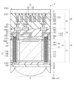
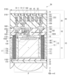
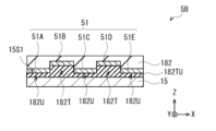
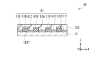
- FIG. 1 is a schematic cross-sectional view showing a configuration example of a lamination cross-section of a photodetector according to a first embodiment of the present disclosure.
- FIG. 2 is a block diagram showing an example of a schematic configuration of the photodetector shown in FIG.
- FIG. 3A is an example of an equivalent circuit diagram of a unit pixel of the photodetector shown in FIG.
- FIG. 3B is a waveform diagram explaining the operation of the pixel circuit shown in FIG. 3A.
- 4A is a schematic cross-sectional view showing a first structural example of a horizontal cross section of the photodetector shown in FIG. 1.
- FIG. 1 is a schematic cross-sectional view showing a configuration example of a lamination cross-section of a photodetector according to a first embodiment of the present disclosure.
- FIG. 2 is a block diagram showing an example of a schematic configuration of the photodetector shown in FIG.
- FIG. 3A is an example of an
- FIG. 4B is a schematic cross-sectional view showing a second configuration example of the horizontal cross section of the photodetector shown in FIG. 1.
- FIG. 4C is a schematic cross-sectional view showing a third configuration example of the horizontal cross section of the photodetector shown in FIG. 1.
- FIG. 4D is a schematic cross-sectional view showing a fourth configuration example of the horizontal cross section of the photodetector shown in FIG. 1.
- FIG. 4E is a schematic cross-sectional view showing a fifth configuration example of the horizontal cross section of the photodetector shown in FIG. 1.
- FIG. 4F is a schematic cross-sectional view showing a sixth configuration example of the horizontal cross section of the photodetector shown in FIG. 1.
- FIG. 4G is a schematic cross-sectional view showing a seventh structural example of the horizontal cross section of the photodetector shown in FIG. 1.
- FIG. 4H is a schematic cross-sectional view showing an eighth configuration example of the horizontal cross section of the photodetector shown in FIG. 1.
- FIG. FIG. 5 is a schematic cross-sectional view showing a configuration example of a lamination cross-section of the photodetector according to the first modification of the first embodiment.
- 6A is a schematic cross-sectional view showing a first structural example of a horizontal cross section of the photodetector shown in FIG. 5.
- FIG. 6B is a schematic cross-sectional view showing a second configuration example of the horizontal cross section of the photodetector shown in FIG. 5.
- FIG. 5 is a schematic cross-sectional view showing a configuration example of the horizontal cross section of the photodetector shown in FIG. 5.
- FIG. 6C is a schematic cross-sectional view showing a third configuration example of the horizontal cross section of the photodetector shown in FIG. 5.
- FIG. FIG. 7A is a schematic cross-sectional view showing a configuration example of a lamination cross-section of a photodetector according to a second modification of the first embodiment
- FIG. 7B is a schematic cross-sectional view showing a configuration example of a horizontal cross section of the photodetector shown in FIG. 7A
- 8A is a schematic cross-sectional view of lamination representing one step of the method for manufacturing the photodetector shown in FIG. 5.
- FIG. FIG. 8B is a schematic diagram of a lamination cross section showing one step following FIG. 8A.
- FIG. 8C is a schematic diagram of a lamination cross section showing one step following FIG. 8B.
- FIG. 8D is a schematic diagram of a lamination cross section showing one step following FIG. 8C.
- FIG. 8E is a schematic diagram of a lamination cross section showing one step following FIG. 8D.
- FIG. 8F is a schematic diagram of a lamination cross section showing one step following FIG. 8E.
- FIG. 8G is a schematic diagram of a lamination cross section showing one step following FIG. 8F.
- FIG. 8H is a schematic diagram of a lamination cross section showing one step following FIG. 8G.
- FIG. 8I is a schematic diagram of a lamination cross section showing one step following FIG. 8H.
- FIG. 8J is a schematic diagram of a lamination cross section showing one step following FIG. 8I.
- FIG. 9 is a schematic cross-sectional view showing a configuration example of a lamination cross-section of the photodetector according to the second embodiment of the present disclosure.
- 10A is a schematic cross-sectional view showing one structural example of a horizontal cross section of the photodetector shown in FIG. 9.
- FIG. 10B is a schematic cross-sectional view showing one configuration example of a horizontal cross section of the photodetector shown in FIG. 9.
- FIG. 11 is a schematic cross-sectional view showing a configuration example of a lamination cross-section of a photodetector according to the first modification of the second embodiment.
- FIG. 12 is a schematic cross-sectional view showing a configuration example of a lamination cross-section of a photodetector according to a second modification of the second embodiment.
- 13A is a schematic cross-sectional view showing a configuration example of a lamination cross-section of a photodetector according to a third modification of the second embodiment;
- FIG. 13B is a schematic diagram showing a planar configuration example (planar layout) of the photodetector shown in FIG. 13A.
- 14A is a schematic cross-sectional view showing a configuration example of a lamination cross-section of a photodetector according to a fourth modification of the second embodiment;
- FIG. 14B is a schematic diagram illustrating a planar configuration example (planar layout) of the photodetector illustrated in FIG. 14A.
- FIG. 15 is a schematic cross-sectional view showing a configuration example of a lamination cross-section of the photodetector according to the third embodiment of the present disclosure.
- 16A is a schematic cross-sectional view showing a first structural example of a horizontal cross section of the photodetector shown in FIG. 15.
- FIG. 16B is a schematic cross-sectional view showing a second configuration example of the horizontal cross section of the photodetector shown in FIG. 15.
- FIG. FIG. 17 is a schematic cross-sectional view showing a configuration example of a lamination cross-section of the photodetector according to the first modification of the third embodiment.
- FIG. 18 is a schematic cross-sectional view showing a configuration example of a lamination cross-section of the photodetector according to the fourth embodiment of the present disclosure.
- 19A is a schematic diagram showing a first structural example of a planar structural example (planar layout) of the photodetector shown in FIG. 18.
- FIG. 19B is a schematic diagram illustrating a second configuration example of the planar configuration example (planar layout) of the photodetector illustrated in FIG. 18.
- FIG. FIG. 20 is an example of an equivalent circuit diagram of a unit pixel of the photodetector shown in FIG. FIG.
- 21A is a schematic diagram illustrating a configuration example of a planar configuration example (planar layout) of a photodetector according to the first modification of the fourth embodiment
- FIG. 21B is a schematic diagram showing a configuration example of a planar configuration example (planar layout) of the photodetector according to the second modification of the fourth embodiment
- 21C is a schematic diagram illustrating a configuration example of a planar configuration example (planar layout) of the photodetector according to the third modification of the fourth embodiment
- FIG. FIG. 22 is a schematic cross-sectional view showing a configuration example of a lamination cross-section of the photodetector according to the fifth embodiment of the present disclosure.
- FIG. 23 is an enlarged cross-sectional view showing an enlarged part of the photodetector shown in FIG. 22.
- FIG. FIG. 24 is a schematic diagram showing a configuration example of a planar configuration example (planar layout) of the photodetector shown in FIG. 25A is a schematic cross-sectional view of a lamination showing one step of the method for manufacturing the photodetector shown in FIG. 22.
- FIG. FIG. 25B is a schematic diagram of a lamination cross section showing one step following FIG. 25A.
- FIG. 25C is a schematic diagram of a lamination cross section showing one step following FIG. 25B.
- FIG. 25D is a schematic diagram of a lamination cross section showing one step following FIG. 25C.
- FIG. 25E is a schematic diagram of a lamination cross section showing one step following FIG. 25D.
- FIG. 25F is a schematic diagram of a lamination cross section showing one step following FIG. 25E.
- FIG. 25G is a schematic diagram of a lamination cross section showing one step following FIG. 25F.
- FIG. 25H is a schematic diagram of a lamination cross section showing one step following FIG. 25G.
- FIG. 25I is a schematic diagram of a lamination cross section showing one step following FIG. 25H.
- FIG. 26 is an enlarged cross-sectional view showing an enlarged part of the photodetector according to the first modification of the fifth embodiment of the present disclosure.
- FIG. 27A is a schematic cross-sectional view of a lamination showing one step of the method for manufacturing the photodetector shown in FIG. 26.
- FIG. FIG. 27B is a schematic diagram of a lamination cross section showing one step following FIG. 27A.
- FIG. 27C is a schematic diagram of a lamination cross section showing one step following FIG. 27B.
- FIG. 27D is a schematic diagram of a lamination cross section showing one step following FIG. 27C.
- FIG. 27E is a schematic diagram of a lamination cross section showing one step following FIG. 27D.
- FIG. 27F is a schematic diagram of a lamination cross section showing one step following FIG. 27E.
- FIG. 28 is an enlarged cross-sectional view showing an enlarged part of the photodetector according to the second modification of the fifth embodiment of the present disclosure.
- FIG. 29 is an enlarged cross-sectional view showing an enlarged part of the photodetector according to the third modification of the fifth embodiment of the present disclosure.
- FIG. 30 is an enlarged cross-sectional view showing an enlarged part of the photodetector according to the fourth modification of the fifth embodiment of the present disclosure.
- FIG. 31 is an enlarged cross-sectional view showing an enlarged part of the photodetector according to the fifth modification of the fifth embodiment of the present disclosure.
- FIG. 32A is an enlarged plan view showing an enlarged part of the photodetector according to the sixth modification of the fifth embodiment of the present disclosure.
- FIG. 32B is an enlarged cross-sectional view showing an enlarged part of the photodetector shown in FIG. 32A.
- FIG. 33 is an enlarged plan view showing an enlarged part of the photodetector according to the seventh modification of the fifth embodiment of the present disclosure.
- FIG. 34 is a functional block diagram showing an example of an electronic device using the photodetector shown in FIG. 1 and the like.
- FIG. 35 is a block diagram showing an example of a schematic configuration of a vehicle control system.
- FIG. 36 is an explanatory diagram showing an example of installation positions of the vehicle exterior information detection unit and the imaging unit.
- the above patent document discloses a structure in which a quench resistor is connected to the cathode via a metal electrode.
- the high-concentration layer is formed by, for example, ion implantation.
- ion implantation may cause crystal defects.
- the Si substrate may be damaged during the formation of the metal electrodes. Such a possibility is a factor in reducing the reliability of APDs.
- the graphene layer constitutes the quench resistor in the above patent document, a certain length is required in order to secure a sufficient resistance value as the quench resistor, which may hinder miniaturization. Therefore, the applicant of the present application has come to provide a highly reliable photodetector that is compatible with miniaturization.
- FIG. 1 schematically illustrates an example of a cross-sectional configuration of a photodetector 1 according to the first embodiment of the present disclosure.
- FIG. 2 is a block diagram showing a schematic configuration of the photodetector 1 shown in FIG. 3A is a circuit diagram showing an example of an equivalent circuit of the unit pixel P of the photodetector 1 shown in FIG. 1.
- FIG. The photodetector 1 can be applied to, for example, a distance image sensor (distance image apparatus 1000 described later, see FIG. 34), an image sensor, or the like that measures distance by the ToF (Time-of-Flight) method.
- a distance image sensor distance image apparatus 1000 described later, see FIG. 34
- ToF Time-of-Flight
- the photodetector 1 has, for example, a pixel array section 100A in which a plurality of unit pixels P are arranged in an array in row and column directions.
- the photodetector 1 has a pixel array section 100A and a bias voltage application section 110, as shown in FIG.
- the bias voltage applying section 110 applies a bias voltage to each unit pixel P of the pixel array section 100A.
- a case of reading electrons as signal charges will be described.
- the unit pixel P includes a light receiving element 12, a clamp circuit 50 as a protection circuit, a first control transistor 71, a current source 72, a terminal 73, and a second control transistor 74. , and a readout circuit 75 .
- the light receiving element 12 converts incident light into an electric signal by photoelectric conversion and outputs the electric signal. Additionally, the light-receiving element 12 converts incident light (photons) into an electrical signal by photoelectric conversion, and outputs a pulse corresponding to the incidence of the photons.
- the light receiving element 12 is, for example, a SPAD element.
- the SPAD element forms an avalanche multiplication region (depletion layer) 12X, for example, by applying a large negative voltage to the cathode, and generates light in response to the incidence of one photon. It has the characteristic that electrons cause avalanche multiplication and a large current flows.
- the anode of the light receiving element 12 is connected, for example, to the bias voltage applying section 110 .
- the cathode of the light receiving element 12 is connected to a terminal 73 to which a power supply voltage VDD is applied via, for example, a first control transistor 71 and a current source 72 .
- a power supply voltage VDD for example, a voltage of about 3V is applied.
- a cathode of the light receiving element 12 is connected to a source terminal of the first control transistor 71 .
- a device voltage VB is applied to the anode of the light receiving element 12 from a device voltage applying section.
- the device voltage VB a large negative voltage at which avalanche multiplication occurs, that is, a voltage higher than the breakdown voltage (for example, about -20 V) is applied.
- the first control transistor 71 is composed of a p-type MOSFET (Metal-Oxide-Semiconductor Field-Effect Transistor) and is also called a quenching resistance element.
- the first control transistor 71 is connected in series with the light receiving element 12 via the clamp circuit 50 .
- the source terminal of the first control transistor 71 is connected to the cathode of the light receiving element 12 and the drain terminal of the first control transistor 71 is connected to the terminal 73 via the current source 72 .
- the first control transistor 71 becomes conductive when the enable signal EN applied to the gate electrode becomes low level, and the current from the current source 72 flows to the light receiving element 12 .
- the second control transistor 74 is connected between the cathode of the light receiving element 12 and a reference potential node (eg, ground).
- the second control transistor 74 is, for example, an N-type MOS transistor.
- the second control transistor 74 becomes conductive when the signal xEN opposite in phase to the enable signal EN is applied to the gate electrode, and makes the voltage applied to the light receiving element 12 equal to or lower than the breakdown voltage. It is designed to be in an activated state.
- the readout circuit 75 is, for example, a CMOS inverter circuit including a P-type MOS transistor Qp and an N-type MOS transistor Qn.
- the readout circuit 75 has an input terminal connected to the cathode of the light receiving element 12, the source terminal of the first control transistor 71, and the second control transistor 74, and an output terminal connected to the arithmetic processing section 76, which will be described later. .
- the readout circuit 75 outputs a received light signal based on the carrier (signal charge) multiplied by the light receiving element 12 . More specifically, the readout circuit 75 shapes the voltage generated by the electrons multiplied by the light receiving element 12 .
- the readout circuit 75 outputs, to the arithmetic processing section 76, a light reception signal, for example, a pulse waveform generated from the arrival time of one photon.
- a light reception signal for example, a pulse waveform generated from the arrival time of one photon.
- the arithmetic processing unit 76 calculates the distance for each unit pixel P by performing arithmetic processing to obtain the distance to the object based on the timing at which a pulse indicating the arrival time of one photon is generated in each light reception signal. Based on these distances, a distance image is generated in which the distances to the subject detected by the plurality of unit pixels P are arranged two-dimensionally.
- the clamp circuit 50 is a protection circuit provided between the light receiving element 12 and the input end of the readout circuit 75 .
- the clamp circuit 50 suppresses the P-type MOS transistor Qp and the N-type MOS transistor Qn constituting the readout circuit 75 and the first control transistor from an overvoltage generated when the light receiving element 12 is irradiated with a large amount of laser light, for example.
- 71 and the second control transistor 74 are overvoltage protection circuits.
- the clamp circuit 50 between the light receiving element 12 and the input terminal of the readout circuit 75, even if the light receiving element 12 is irradiated with a large amount of laser light exceeding a predetermined light amount (more than expected), Even if there is, the read circuit 75 and the like can be protected from overvoltage.
- the clamp circuit 50 has, for example, a resistive element 51, a first clamp element 54, and a second clamp element 55, as specifically shown in FIG.
- One end of the resistance element 51 is connected to the cathode electrode of the light receiving element 12 .
- the first clamp element 54 is, for example, a clamp diode having a cathode connected to the other end (output end) of the resistance element 51 and an anode connected to a reference potential node (eg, ground).
- the resistance element 51 is provided to limit the current value flowing through the first clamping element 54 so as not to exceed its rated forward current when overvoltage occurs in the light receiving element 12 .
- the clamp diode which is the first clamp element 54, clamps the overvoltage to a constant voltage (forward voltage VF) when an overvoltage exceeding the clamp voltage occurs in the light receiving element 12.
- first clamping element 54 is not limited to a clamping diode.
- a Schottky barrier diode or the like can be used as the first clamping element 54 in addition to the clamping diode.
- the second clamp element 55 is composed of, for example, a P-type MOS transistor.
- the second clamping element 55 is connected between the first clamping element 72 (for example, the anode of the clamping diode) and a node N to which the input terminal of the readout circuit 75 is connected.
- a P-type MOS transistor as the second clamp element 55 has a gate electrode connected to a reference potential node (for example, ground) and a back gate connected to a source electrode.
- the clamping operation when an overvoltage of minus several tens of volts is generated in the light receiving element 12 will be described with reference to the waveform diagram of FIG. 3B.
- the clamp diode as the first clamp element 54 clamps the overvoltage generated in the light receiving element 12 to a constant voltage (forward voltage VF). Due to this clamping operation, the overvoltage generated in the light receiving element 12 is clamped to a negative voltage of about -1V to -3V, for example.
- the negative voltage when a negative voltage is generated by the clamping operation of the first clamping element 54, the negative voltage may exceed the withstand voltage of the MOS transistor, which will be described later.
- a second clamping device 55 is provided to address this negative voltage problem. That is, the second clamp element 55 clamps the voltage of the node N to which the input terminal of the readout circuit 75 is connected to the gate-source voltage Vgs (for example, about 0.5 V) of the P-type MOS transistor. As a result, the clamping operation of the first clamping element 54 can solve the negative voltage problem.
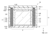
- the photodetector 1 is a so-called back-illuminated photodetector.
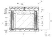
- the photodetector 1 includes, for example, a logic substrate 20 laminated on a surface of a sensor substrate 10 (for example, a first surface 11S1 which is a surface of a semiconductor substrate 11 constituting the sensor substrate 10). Light is received from the rear surface of the sensor substrate 10 (the second surface 11S2, which is the rear surface of the semiconductor substrate 11 forming the sensor substrate 10).
- the photodetector 1 has a light receiving element 12 for each unit pixel P. As shown in FIG.
- the light-receiving element 12 has a light-receiving portion 13 and a multiplier portion 14 , and the light-receiving portion 13 is embedded in the semiconductor substrate 11 .
- Semiconductor substrate 11 further includes p-type semiconductor region (p+) 14X among p-type semiconductor region (p+) 14X and n-type semiconductor region (n+) 14Y forming multiplier section 14 on first surface 11S1. It is A semiconductor layer 15 is provided on the first surface 11S1 side of the semiconductor substrate 11 .
- the semiconductor layer 15 is provided with an n-type semiconductor region (n+) 14 ⁇ /b>Y forming the multiplier section 14 .
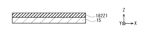
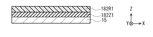
- the sensor substrate 10 has, for example, a semiconductor substrate 11 made of a silicon substrate, a semiconductor layer 15, and a multilayer wiring layer 18.
- the semiconductor substrate 11 has a first surface 11S1 and a second surface 11S2 facing each other.
- the semiconductor substrate 11 has a p-well (p) 111 common to a plurality of unit pixels P.
- the semiconductor substrate 11 is provided with an n-type semiconductor region (n) 112 whose impurity concentration is controlled to be n-type, for example, for each unit pixel P, thereby forming a light receiving element 12 for each unit pixel P.
- n semiconductor region
- the semiconductor substrate 11 is further provided with a pixel separation portion 17 extending from the first surface 1S1 to the second surface 11S2.
- the light receiving element 12 has a multiplication region for avalanche multiplication of carriers by a high electric field region, that is, an avalanche multiplication region.
- the light receiving element 12 is a SPAD capable of forming an avalanche multiplication region (depletion layer) by applying a large positive voltage to the cathode and avalanche-multiplying electrons generated by the incidence of one photon. element.
- the light receiving element 12 has a light receiving section 13 and a multiplier section 14 .
- the light receiving section 13 performs photoelectric conversion by absorbing light incident from the second surface 11S2 side of the semiconductor substrate 11 and generating carriers according to the amount of received light.
- the light receiving portion 13 includes the n-type semiconductor region (n) 112 whose impurity concentration is controlled to be n-type, as described above. Carriers (electrons) generated in the light receiving section 13 are transferred to the multiplication section 14 due to the potential gradient. Note that the light receiving unit 13 is a specific example corresponding to the “light receiving unit” of the present disclosure.
- the multiplication unit 14 avalanche-multiplies the carriers (here, electrons) generated in the light receiving unit 13 .
- the multiplication unit 14 includes, for example, a p-type semiconductor region (p+) 14X having a higher impurity concentration than the p-well (p) 111 and an n-type semiconductor region (n+) 14X having a higher impurity concentration than the n-type semiconductor region (n) 112. ) 14Y.
- the p-type semiconductor region (p+) 14X is provided in the semiconductor substrate 11 so as to face the first surface 11S1.
- the n-type semiconductor region (n+) 14Y is provided so as to protrude from the first surface 11S1 of the semiconductor substrate 11 .
- the multiplier 14 is a specific example corresponding to the “multiplier” of the present disclosure.
- a p-type semiconductor region (p+) 14X provided facing the first surface 11S1 of the semiconductor substrate 11 and an n-type semiconductor region (p+) provided facing the second surface 15S2 of the semiconductor layer 15
- An avalanche multiplication region 12X is formed at the junction with n+) 14Y.
- the avalanche multiplication region 12X is a high electric field region, ie a depletion layer, formed by a large negative voltage applied to the anode.
- the avalanche multiplication region 12X is formed at the interface between the p-type semiconductor region (p+) 14X and the n-type semiconductor region (n+) 14Y. In the avalanche multiplication region 12X, electrons (e ⁇ ) generated by one photon incident on the light receiving element 12 are multiplied.
- the semiconductor layer 15 is a semiconductor layer made of silicon, for example, formed on the first surface 11S1 of the semiconductor substrate 11 using, for example, an epitaxial crystal growth method, and corresponds to a specific example of the "semiconductor layer" of the present disclosure. It is.
- the semiconductor layer 15 has a first surface 15S1 and a second surface 15S2 facing each other.
- the first surface 15 S 1 faces the multilayer wiring layer 18 and the second surface 15 S 2 faces the semiconductor substrate 11 .
- the semiconductor layer 15 is embedded with the n-type semiconductor region (n+) 14Y facing the second surface 15S2.
- a contact electrode 16 is further provided on the n-type semiconductor region (n+) 14Y so as to face the first surface 15S1.
- the contact electrode 16 is a cathode as a specific example corresponding to the “first electrode” of the present disclosure, and is electrically connected to the multiplier section 14 .
- the contact electrode 16 is composed of, for example, an n-type semiconductor region (n++) having a higher impurity concentration than the n-type semiconductor region (n+) 14Y.
- the pixel separating section 17 electrically separates the adjacent unit pixels P, and is provided in the pixel array section 100A in a grid pattern so as to surround each of the plurality of unit pixels P in plan view, for example. .
- the pixel separating portion 17 extends from the second surface 11S2 of the semiconductor substrate 11 to the first surface 15S1 of the semiconductor layer 15. As shown in FIG. That is, the pixel separating portion 17 penetrates the semiconductor substrate 11 and the semiconductor layer 15 .
- the pixel separation section 17 is formed using insulating films 17B and 17C such as silicon oxide (SiOx) films and a light shielding film 17A.
- a p-type semiconductor region (p+) 113 having a higher impurity concentration than the p-well 111 is provided around the pixel isolation portion 17 .
- the p-type semiconductor region (p+) 113 includes an extension portion 113X extending toward the inside of the unit pixel P in the vicinity of the first surface 11S1 of the semiconductor substrate 11 (see FIG. 1).
- the extended portion 113X is an anode as a specific example corresponding to the “second electrode” of the present disclosure, and also serves as a contact electrode electrically connected to the light receiving portion 13 .
- the p-type semiconductor region (p+) 113 further extends along the second surface 11S2 of the semiconductor substrate 11. As shown in FIG.
- a semiconductor layer 15 and a multilayer wiring layer 18 are laminated in order on the first surface 11S1 of the semiconductor substrate 11 opposite to the second surface 11S2, which is the light incident surface.
- a wiring layer 181 made up of one or more wirings is embedded in an interlayer insulating layer 182 .
- the wiring layer 181 is, for example, a path for supplying a voltage to be applied to the semiconductor substrate 11 and the light receiving element 12 and extracting carriers generated in the light receiving element 12 .
- Some of the wirings in the wiring layer 181 are electrically connected to the contact electrodes 16 and the extended portions 113X through the vias V1.
- a plurality of pad electrodes 183 are embedded in the vicinity of the surface of the interlayer insulating layer 182 opposite to the semiconductor substrate 11 (the surface 18S1 of the multilayer wiring layer 18).
- the plurality of pad electrodes 183 are electrically connected to some wirings of the wiring layer 181 via vias V2.
- FIG. 1 shows an example in which one wiring layer 181 is formed in the multilayer wiring layer 18, the number of layers of the wiring layers 181 embedded in the multilayer wiring layer 18 is not limited.
- a wiring layer may be formed.
- the interlayer insulating layer 182 is, for example, a single layer film made of one of silicon oxide (SiOx), TEOS, silicon nitride (SiNx) and silicon oxynitride (SiOxNy), or made of two or more of these. It is composed of a laminated film.
- the wiring layer 181 is formed using, for example, aluminum (Al), copper (Cu), tungsten (W), or the like.
- the pad electrode 183 is exposed on the surface 18S1 of the multilayer wiring layer 18, which is the bonding surface with the logic substrate 20. As shown in FIG. The pad electrode 183 is used for connection with the logic substrate 20, for example.
- the pad electrode 183 is formed using copper (Cu), for example.
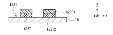
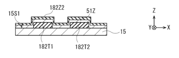
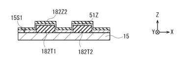
- a resistance element 51 is further provided in the interlayer insulating layer 182 .
- the resistor element 51 is electrically connected to the contact layer 16 and is a resistor made of a polycrystalline semiconductor material such as polysilicon (Poly-Si) containing an n-type impurity element.
- the resistive element 51 is, for example, the first It has a body portion 52 extending parallel to the surface 11S1, that is, extending along the XY plane, and a lead-out portion 53 connecting the body portion 52 and the contact layer 16 .
- the body portion 52 is formed on the same layer as the wiring layer 181 in the example of the structure shown in FIG. However, the body portion 52 of the resistance element 51 may be provided on a layer different from the wiring layer 181 .
- the distance between the lower surface of the body portion 52 and the upper surface of the contact layer 16, that is, the thickness G1 of the portion of the interlayer insulating layer 182 sandwiched between the body portion 52 and the contact layer 16 (see FIG. 1) is preferably greater than 150 nm when the dielectric constant ⁇ of the material forming the interlayer insulating layer 182 is 4.2. If the thickness G1 is smaller than this, a strong electric field is generated at an unintended location between the main body portion 52 and the multiplier portion 14, that is, at a location other than the first connection portion C1, and unintended avalanche multiplication of electrons occurs. This is because it may occur.
- a via V2 is provided upright on the upper surface of the main body portion 52 .
- the resistance element 51 is electrically connected to the pad electrode 183 through the via V2.
- another wiring layer such as the wiring layer 181 may be further provided between the body portion 52 and the via V2, for example.
- the via V2 connected to the resistance element 51 is a specific example corresponding to the "first wiring" of the present disclosure.
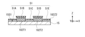
- the position in the XY plane of the first connection portion C1 between the extraction portion 53 of the resistance element 51 and the contact layer 16 and the main body portion 52 of the resistance element 51 and the positions of the second connecting portion C2 with the via V2 in the XY plane are preferably different from each other in the XY plane. That is, it is preferable that the lead-out portion 53 and the via V2 are arranged so as not to overlap each other in the stacking direction (Z-axis direction) orthogonal to the first surface 11S1. This is because the resistance value of the resistance element 51, that is, the resistance value between the contact layer 16 and the via V2 increases in proportion to the path length L52.
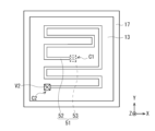
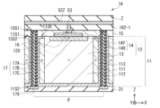
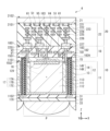
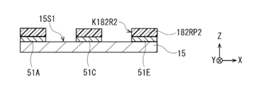
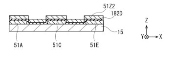
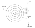
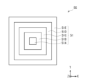
- 4A is a schematic cross-sectional view showing a first configuration example (planar layout) of the XY cross section of the photodetector 1.
- the first connection portion C1 is located, for example, in the central region of the pixel P in the XY plane, and the second connection portion C2 is located in the peripheral region of the pixel P in the XY plane. do.
- the main body portion 52 extends linearly in the XY plane, but the present disclosure is not limited to this.
- the body portion 52 includes one bent portion on the path from the first connection portion C1 to the second connection portion C2.
- the body portion 52 includes two bent portions on the route from the first connection portion C1 to the second connection portion C2.
- the body portion 52 includes three bent portions on the route from the first connection portion C1 to the second connection portion C2. Furthermore, in the fifth configuration example of FIG. 4E, the body portion 52 spirally extends from the central region of the pixel P toward the peripheral region of the pixel P in the XY plane. In FIG. 4E, the body portion 52 has a shape that makes only about one turn, but in the present disclosure, the body portion 52 may have a spiral shape that makes multiple turns.
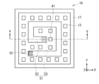
- 4B to 4E are schematic cross-sectional views showing second to fifth configuration examples of the XY cross section of the photodetector 1. FIG.
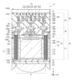
- the shape of the body portion 52 in the XY plane is not limited to being spiral, and may include a serpentine portion, as shown in FIG. 4F, for example.
- the width of the body portion 52 may be smaller than the dimensions of the lead-out portion 53 in the XY plane and the dimensions of the via V2 in the XY plane.
- FIG. 4F is a schematic cross-sectional view showing a sixth configuration example of the XY cross section of the photodetector 1 .
- the first portion 52-1 is a portion of the body portion 52 that is connected to the extraction portion 53
- the second portion 52-2 is a portion of the body portion 52 that is connected to the via V2
- 52-3 is a central portion in the longitudinal direction connecting the first portion 52-1 and the second portion 52-2 of the body portion 52.
- the third portion 52-3 has the highest volume resistivity, and the first portion 52-1 and the second portion 52-2 are lower than the third portion 52-3. It is preferable to have volume resistivity.
- the third portion 52-3 may be made to have a high resistance.
- the third portion 52-3 may be made to have a high resistance.
- the resistance of the third portion 52-3 may be increased by adding at least one of O (oxygen) and N (nitrogen) to the third portion 52-3 and performing heat treatment.
- Si silicon
- Ar argon
- the resistance of the third portion 52-3 is increased. You may do so.
- the width of the third portion 52-3 of the main body portion 52 is set to the width of the first portion 52-1, for example, as in the eighth configuration example of the XY cross section of the photodetector 1 shown in FIG. 4H. and the width of the second portion 52-2 to increase the resistance of the third portion 52-3.
- the logic board 20 has, for example, a semiconductor substrate 21 made of a silicon substrate and a multilayer wiring layer 22 .
- the logic board 20 includes, for example, the bias voltage application section 110 described above, a readout circuit for outputting pixel signals based on charges output from the unit pixels P of the pixel array section 100A, a vertical drive circuit, a horizontal drive circuit, and an output circuit.
- a logic circuit including circuits and the like is configured. Note that the logic circuit may include a column signal processing circuit.
- a gate wiring 221 of a transistor constituting a readout circuit and wiring layers 222, 223, 224, 225 including one or more wirings are stacked in order from the semiconductor substrate 21 side.
- An interlayer insulating layer 226 is provided in the gap between the gate wiring 221 of the transistor and the wiring layers 222, 223, 224, 225 including one or more wirings.
- a plurality of pad electrodes 227 are embedded in a surface 22S1 of the multilayer wiring layer 22, which is the surface of the interlayer insulating layer 226 opposite to the semiconductor substrate 21. As shown in FIG. The plurality of pad electrodes 227 are electrically connected to some wirings of the wiring layer 225 via vias V3.
- the interlayer insulating layer 117 is, for example, a single-layer film made of one of silicon oxide (SiOx), TEOS, silicon nitride (SiNx), silicon oxynitride (SiOxNy), or the like. It is composed of a laminated film composed of two or more kinds of single-layer films.
- the gate wiring 221 and the wiring layers 222, 223, 224, and 225 are formed using, for example, aluminum (Al), copper (Cu), or tungsten (W), like the wiring layer 181.
- the pad electrodes 227 are exposed on the surface 22S1 of the multilayer wiring layer 22, which is the joint surface with the sensor substrate 10, and are connected to the pad electrodes 183 of the sensor substrate 10, for example.
- the pad electrode 227 is formed using copper (Cu), for example, like the pad electrode 183 .
- the pad electrode 183 and the pad electrode 227 are, for example, CuCu bonded.
- the cathode of the light receiving element 12 is electrically connected to the quenching resistance element 120 provided on the logic substrate 20 side, and the anode of the light receiving element 12 is electrically connected to the bias voltage applying section 110 .
- a microlens 33 is provided for each unit pixel P, for example, via a passivation film 31 and a color filter 32, for example.
- the microlens 33 converges the light incident from above onto the light receiving element 12, and is made of, for example, silicon oxide (SiOx).
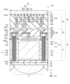
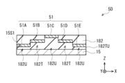
- FIG. 5 schematically illustrates an example of a layered cross-sectional configuration of a photodetector 1A as a first modified example according to the first embodiment of the present disclosure.
- 6A to 6C are schematic cross-sectional views showing first to third configuration examples (planar layout) of the XY cross section of the photodetector 1A shown in FIG. 5, respectively.
- the photodetector 1A further includes a reflective layer 41 as shown in FIGS. 5 and 6A to 6C.
- the configuration of the photodetector 1A is substantially the same as the configuration of the photodetector 1, except that the reflective layer 41 is further provided.
- a plurality of reflective layers 41 are discretely arranged along the XY plane around the body portion 52 , for example, on the same layer as the body portion 52 .
- the reflective layer 41 can be formed using, for example, a wiring material having light reflectivity such as aluminum (Al).
- the reflective layer 41 can also be formed using a nonmetallic material such as silicon oxide.
- the reflective layer 41 may be made of the same kind of material as the polycrystalline semiconductor material forming the body portion 52 .
- the reflective layer 41 is provided in the photodetector 1A of this modified example.
- the light transmitted through the light receiving section 13 without being absorbed is reflected by the reflective layer 41 and enters the light receiving section 13 again. Therefore, compared with the photodetector 1 that does not have the reflective layer 41, it is possible to further improve the sensitivity to incident light.
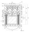
- FIG. 7A schematically illustrates an example of a laminated cross-sectional configuration of a photodetector 1B as a second modified example according to the first embodiment of the present disclosure.
- FIG. 7B is a schematic cross-sectional view showing a configuration example (planar layout) of the XY cross section of the photodetector 1B shown in FIG. 7A.
- the photodetector 1B like the photodetector 1A, further includes a plurality of reflective layers 41 as shown in FIGS. 7A and 7B.
- a plurality of reflective layers 41 are discretely arranged along the XY plane.
- the photodetector 1B further includes a plurality of reflective layers 41 in the layer between the layer on which the body portion 52 is provided and the layer on which the contact layer 16 is provided.
- the body portion 52 and one reflective layer 41C of the plurality of reflective layers 41 overlap in the thickness direction (Z-axis direction).
- the reflective layer 41 ⁇ /b>C may electrically connect the body portion 52 and the contact layer 16 .
- the reflective layer 41C is connected to the body portion 52 through the extraction portion 53, and is connected to the contact layer 16 through the via V2.
- the reflective layer 41 can be formed using, for example, a wiring material having light reflectivity such as aluminum (Al).
- the reflective layer 41 can also be formed using a nonmetallic material such as silicon oxide.
- the reflective layer 41 may be made of the same kind of polycrystalline semiconductor material as the polycrystalline semiconductor material forming the body portion 52, or may be made of a polycrystalline semiconductor material different in kind from the polycrystalline semiconductor material forming the body portion 52. It may be configured by
- FIGS. 8A to 8J are schematic cross-sectional views of laminated layers representing one step of the method for manufacturing the photodetector 1A.
- a semiconductor substrate 11 is prepared.
- a p-well (p) 111, an n-type semiconductor region (n) 112, a p-type semiconductor region (p+) 113 and p-type semiconductor regions (p+) 113 are formed in the semiconductor substrate 11 by controlling the concentration of p-type or n-type impurities.
- type semiconductor regions (p+) 14X are respectively formed.
- a semiconductor layer 15 made of, for example, silicon (Si) is formed on the first surface 11S1 of the semiconductor substrate 11 by an epitaxial crystal growth method such as a metal organic chemical vapor deposition (MOCVD) method. do.
- MOCVD metal organic chemical vapor deposition
- the semiconductor layer 15 and the semiconductor substrate are etched by etching. 11 is formed through a through hole.
- the insulating films 17B and 17C and the light shielding film 17A are sequentially formed inside the through holes by, for example, a CVD (Chemical Vapor Deposition) method, a PVD (Physical Vapor Deposition) method, an ALD (Atomic Layer Deposition) method, or a vapor deposition method. film.
- CVD Chemical Vapor Deposition
- PVD Physical Vapor Deposition
- ALD Atomic Layer Deposition
- an interlayer insulating layer 182-1 is formed on the first surface 15S1 of the semiconductor layer 15, as shown in FIG. 8B.
- the first surface 15S1 of the semiconductor layer 15 may be planarized by, for example, CMP (Chemical Mechanical Polishing) before forming the interlayer insulating layer 182-1.
- a resist mask R1 including an opening R1K is formed on the interlayer insulating layer 182-1 by photolithography. Further, a through hole TH1 is formed in the interlayer insulating layer 182-1 by dry etching such as RIE using the resist mask R1 or wet etching. The through hole TH1 is formed at a position overlapping the p-type semiconductor region (p+) 14X near the center of the light receiving portion 13. As shown in FIG. After forming the through hole TH1, the resist mask R1 is removed.
- a polycrystalline semiconductor material such as polysilicon doped with an n-type impurity element such as P (phosphorus) or As (arsenic) is deposited so as to cover the interlayer insulating layer 182-1. is used to form a polycrystalline semiconductor layer 52Z.
- a film of pure polysilicon containing no n-type impurities may be formed, and then n-type impurities may be ion-implanted.
- the contact layer 16 and the n-type semiconductor region (n+) 14Y are formed in a self-aligned manner by diffusing the n-type impurity from the lead-out portion 53. Therefore, compared with the case of forming by ion implantation, for example, Thus, the contact layer 16 and the n-type semiconductor region (n+) 14Y can be formed in a narrower region with high precision.
- the insulating film Z is removed.
- a photolithographic method is used on the polycrystalline semiconductor layer 52Z to form a resist mask R2 including an opening R2K at a predetermined position.
- the semiconductor layer 52Z is selectively removed by RIE or the like.
- the body portion 52 and the reflective layer 41 are formed at predetermined positions on the interlayer insulating layer 182-1.
- the resistive element 51 composed of the extraction portion 53 and the main body portion 52 is obtained.
- an interlayer insulating layer 182-2 is formed so as to cover the interlayer insulating layer 182-1, the main body portion 52, and the reflective layer 41.
- the upper surface of the interlayer insulating layer 182-2 is planarized in accordance with the above.
- an interlayer insulating layer 182 consisting of an interlayer insulating layer 182-1 and an interlayer insulating layer 182-2 is obtained.
- a portion of the interlayer insulating layer 182 and a portion of the semiconductor layer 15 are selectively removed using, for example, photolithography, and a position corresponding to the extended portion 113X in the Z-axis direction is removed.
- the via V1 is formed by filling the opening with a conductive metal material such as W (tungsten).
- W tungsten
- the interlayer insulating layer 182 around the via V1 is selectively removed to form the wiring layer 181 on the via V1.
- through holes TH2 are formed in the interlayer insulating layer 182.
- the through holes TH2 are formed at a position corresponding to the wiring layer 181 and at a position corresponding to the main body portion 52 .
- vias V2 are formed by filling the through holes TH2 with a conductive metal material such as W (tungsten).
- pad electrodes 183 are formed so as to be in contact with the upper surfaces of the vias V2, and the periphery of the pad electrodes 183 is filled with an interlayer insulating layer 182. Then, as shown in FIG. Furthermore, by flattening the upper surfaces of the pad electrodes 183 and the interlayer insulating layer 182, the multilayer wiring layer 18 having a flat surface 18S1 is obtained. Thereby, the sensor substrate 10 is completed.
- the separately produced logic board 20 is attached to the sensor board 10 .
- a plurality of pad electrodes 183 exposed on the surface 18S1 of the multilayer wiring layer 18 serving as the bonding surface of the sensor substrate 10 and a plurality of pad portions exposed on the surface 22S of the multilayer wiring layer 22 serving as the bonding surface of the logic substrate 20 are formed.
- 217 are Cu—Cu bonded.
- the photodetector 1A shown in FIG. 5 is completed.
- the photodetector 1 of the present embodiment the photodetector 1A as the first modified example, and the photodetector 1B as the second modified example (hereinafter referred to as the photodetector 1 of the present embodiment, etc.) 1
- a resistance element 51 made of a polycrystalline semiconductor material is connected to the contact layer 16 electrically connected to the multiplier section 14 .
- the semiconductor substrate 11 such as a Si substrate does not come into direct contact with the metal, a silicidation reaction between Si and the metal element does not occur, and the metal element can be prevented from entering the semiconductor substrate 11 . can. Therefore, the structural stability of the semiconductor substrate 11 is enhanced as compared with the case where the resistance element 51 is made of metal. That is, since it is possible to suppress the occurrence of crystal structure defects in the semiconductor substrate 11, it is possible to obtain high operational reliability of the semiconductor substrate 11, such as ensuring a sufficient withstand voltage.
- the resistance element 51 has a body portion 52 extending in the XY plane, and a take-out portion 53 extending in the stacking direction (Z-axis direction) so as to connect the contact layer 16 and the body portion 52 . Therefore, the resistance value of the resistance element 51 can be arbitrarily set by forming the body portion 52 in a linear shape and adjusting the length of the path.
- the resistance element 51 is made of a polycrystalline semiconductor such as polysilicon, it is easier to achieve a higher resistance than when the resistance element 51 is made of a metal material, and an unintended parasitic capacitance is also reduced. can be reduced. Furthermore, it is possible to reduce the power consumption required during operation, and it is also advantageous for speeding up.
- the diffusion layer such as the contact layer 16 is manufactured in a self-aligned manner by diffusing the n-type impurity contained in the lead-out portion 53 of the resistance element 51. It is possible. Therefore, it is not necessary to implant ions into the semiconductor substrate 11 to form a diffusion layer, and the crystal structure of the semiconductor substrate 11 can be stably maintained.
- the resistance element 51 constitutes a clamp circuit 50 as a protection circuit. Therefore, it is possible to avoid damage to the readout circuit 75 and the like due to an overvoltage that occurs when the light receiving element 12 is irradiated with a large amount of laser light, for example.
- the photodetection devices 1A and 1B since a plurality of reflection layers 41 are provided, the light that has been incident from the second surface 11S2 and has passed through the light receiving section 13 is reflected and made to enter the light receiving section 13 again. can be done. Therefore, higher photodetection sensitivity can be obtained.
- a single photon avalanche diode (SPAD) element for example, is known as a light receiving element that generates a signal in response to receiving a photon.
- SPAD single photon avalanche diode
- a voltage higher than the breakdown voltage is applied to the anode electrode (or cathode electrode) of the SPAD element to use the SPAD element ( For example, see JP-A-2019-125717).
- the SPAD element when the SPAD element is irradiated with a large amount of laser light more than expected (a predetermined amount of light or more), such as when the SPAD element is directly irradiated with the laser beam, the SPAD element cannot perform photoelectric conversion with the large amount of light. As the influence becomes stronger, the internal impedance drops significantly. As a result, an excessive voltage is applied to the readout circuit that reads out the signal generated by the SPAD element, and the circuit elements constituting the readout circuit may be damaged. Therefore, in order to protect the readout circuit, a configuration has been proposed in which a resistive element made of metal is directly connected to the SPAD element (for example, Japanese Patent Application Laid-Open No. 2020-153929). Recently, however, there has been an increasing demand for further miniaturization of such light receiving elements and photodetectors equipped with such light receiving elements. Under these circumstances, the applicant of the present application has come to provide a highly reliable photodetector that can be miniaturized.
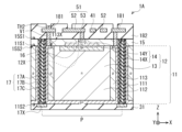
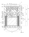
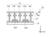
- FIG. 9 schematically illustrates an example of a cross-sectional configuration of the photodetector 2 according to the second embodiment of the present disclosure.
- FIGS. 10A and 10B are schematic cross-sectional views showing one structural example of the horizontal cross section of the photodetector 2 shown in FIG. 9, respectively.
- FIG. 10A represents a horizontal cross section at the height position Lv1 shown in FIG. 9, and
- FIG. 10B represents a horizontal cross section at the height position Lv2 shown in FIG.
- FIG. 9 shows a cross section in the arrow direction along the IX-IX section line shown in FIGS. 10A and 10B.
- the same reference numerals are given to the same components as those of the photodetector 1 of the first embodiment, and the description thereof will be omitted as appropriate.
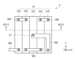
- the via V1 electrically connected to the p-type semiconductor region (p+) 113 as an anode corresponds to the light receiving section 13 of each pixel P in the cross section parallel to the XY plane. It is provided so as to surround the area where the Also, the vias V1 surrounding the light receiving portions 13 of the adjacent pixels P are provided so as to be connected to each other. Therefore, contact resistance on the anode side can be reduced.
- the pixel separation section 17 is provided inside the semiconductor substrate 11 so as to surround the light receiving section 13 in a cross section parallel to the XY plane, and separates the plurality of pixels P from each other.
- the wiring layer 181 is provided so as to form a lattice shape in a cross section parallel to the XY plane so as to overlap the pixel separating portion 17 in the thickness direction (Z-axis direction), and is electrically connected to the via V1.
- the via V1 and the take-out portion 53 are made of a polycrystalline semiconductor material such as polysilicon.
- the wiring layer 181 and the main body 52 are composed of a single layer film made of a metal material such as tungsten.
- the via V2 may be made of Cu (copper).
- the resistance value of the resistive element 51 is, for example, 5 k ⁇ or more.
- the polysilicon forming the extraction portion 53 of the resistance element 51 and the via V1 has an impurity concentration of, for example, 1019 atoms/cm3 or more and less than 1021 atoms/cm3.
- the contact layer 16 electrically connected to the multiplier section 14 is connected to the resistive element 51 including the extraction section 53 made of a polycrystalline semiconductor material.
- the semiconductor substrate 11 such as a Si substrate does not come into direct contact with the metal, a silicidation reaction between Si and the metal element does not occur, and the metal element can be prevented from entering the semiconductor substrate 11 . can. Therefore, the structural stability of the semiconductor substrate 11 is enhanced as compared with the case where the resistance element 51 is made of metal.
- the resistance element 51 constitutes a clamp circuit 50 as a protection circuit. Therefore, it is possible to avoid damage to the readout circuit 75 and the like due to an overvoltage that occurs when the light receiving element 12 is irradiated with a large amount of laser light, for example.
- the vias V1 are provided so as to surround the regions corresponding to the light receiving portions 13 of the pixels P in the cross section parallel to the XY plane, and the vias V1 surrounding the light receiving portions 13 of the adjacent pixels P are provided. are connected to each other. Therefore, contact resistance on the anode side can be reduced.
- the via V1 is not made of a polycrystalline semiconductor material such as polysilicon, but a metal such as W (tungsten) having a lower resistance than the polycrystalline semiconductor material. It may be made of material.
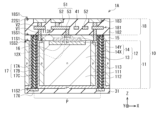
- FIG. 11 schematically illustrates an example of a layered cross-sectional configuration of a photodetector 2A as a first modified example according to the second embodiment of the present disclosure.
- the photodetector 2A is such that the wiring layer 181 and the body portion 52 each have a two-layer structure.
- the configuration of the photodetector 2A is substantially the same as the configuration of the photodetector 2 except for this point.
- the body portion 52 extending parallel to the XY plane has two layers: a first layer 52A in contact with the upper end of the lead-out portion 53 and a second layer 52B that covers the first layer 52A and contacts the via V2. It has a layered structure.
- the wiring layer 181 has a two-layer structure of a first layer 181A in contact with the upper end of the via V1 and a second layer 181B covering the first layer 181A and in contact with the via V2.
- the first layer 52A and the first layer 181A are preferably made of the same material, have the same thickness, and are positioned on substantially the same level.
- the first layer 52A and the first layer 181A are, for example, WSi (tungsten silicon) layers.
- the second layer 52B and the second layer 181B are preferably made of the same material, have the same thickness, and are positioned on substantially the same level.
- the second layer 52B and the second layer 181B are, for example, W (tungsten) layers.
- the lead-out portion 53 and the via V1 made of polysilicon are in contact with the first layer 52A and the first layer 181A, which are WSi (tungsten silicon) layers.
- the extraction portion 53 and the via V1 made of polysilicon are in contact with the body portion 52 and the first layer 181 made of W (tungsten), respectively. there is Therefore, the contact resistance between the extraction portion 53 and the main body portion 52 and the contact resistance between the via V1 and the wiring layer 181 can be stabilized at a lower level than in the photodetector 2 of the second embodiment.
- FIG. 12 schematically illustrates an example of a laminated cross-sectional configuration of a photodetector 2B as a second modified example according to the second embodiment of the present disclosure.
- the photodetector 2B has a via V2 arranged directly above the lead-out portion 53 of the resistive element 51. As shown in FIG. That is, the take-out portion 53 and the via V2 provided on the main body portion 52 are provided at positions overlapping each other in the Z-axis direction.
- the configuration of the photodetector 2B is substantially the same as the configuration of the photodetector 2 except for this point.
- the via V2 is provided directly above the take-out portion 53, so that the dimension of the body portion 52 in the XY plane direction can be further reduced.
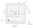
- FIG. 13A schematically illustrates an example of a laminated cross-sectional configuration of a photodetector 2C as a third modified example according to the second embodiment of the present disclosure.
- FIG. 13B is a schematic diagram showing a planar configuration example (planar layout) of the photodetector 2C shown in FIG. 13A. Note that FIG. 13A shows a cross section in the arrow direction along the XIIIA-XIIIA cutting line shown in FIG. 13B. Also, FIG. 13B shows an XY cross section of a layer including the reflective layer 41 and the like.
- the photodetector 2C further includes a plurality of reflective layers 41 as shown in FIGS. 13A and 13B. Except for this point, the configuration of the photodetector 2C is the same as that of the photodetector 2B.
- a plurality of reflective layers 41 are discretely arranged along the XY plane. Specifically, the plurality of reflective layers 41 are arranged two-dimensionally periodically to form a check pattern along the XY plane. That is, a gap is provided between the reflective layers 41 adjacent to each other in the X-axis direction and the Y-axis direction.
- the multiple reflective layers 41 are provided on the same layer as the main body 52 and the wiring layer 181 , for example.
- the multiple reflective layers 41 are made of a polycrystalline semiconductor such as polysilicon.
- the body portion 52 and the wiring layer 181 are preferably made of the same kind of constituent material as the constituent material of the reflective layer 41 (the same kind of polycrystalline semiconductor such as polysilicon). This is because the reflective layer 41, the body portion 52, and the wiring layer 181 can be formed collectively.
- the photodetector 2C of this modified example since a plurality of reflective layers 41 are provided, the light that is incident from the second surface 11S2 and has passed through the light receiving section 13 is reflected, can be made incident on Therefore, higher photodetection sensitivity can be obtained.
- FIG. 14A schematically illustrates an example of a laminated cross-sectional configuration of a photodetector 2D as a fourth modified example according to the second embodiment of the present disclosure.
- FIG. 14B is a schematic diagram showing a planar configuration example (planar layout) of the photodetector 2D shown in FIG. 14A. It should be noted that FIG. 14A represents a cross section in the arrow direction along the XIVA-XIVA cutting line shown in FIG. 14B.
- the photodetector 2C further includes a plurality of reflective layers 41 and a plurality of reflective layers 42, as shown in FIGS. 14A and 14B. Except for this point, the configuration of the photodetector 2D is the same as that of the photodetector 2B.
- a plurality of reflective layers 41 are discretely arranged along the XY plane. Specifically, the plurality of reflective layers 41 are arranged two-dimensionally periodically to form a check pattern along the XY plane. That is, a gap is provided between the reflective layers 41 adjacent to each other in the X-axis direction and the Y-axis direction. In the photodetector 2 ⁇ /b>D, the multiple reflective layers 41 are provided on the same layer as the main body 52 and the wiring layer 181 , for example.
- the multiple reflective layers 41 are made of a polycrystalline semiconductor such as polysilicon.
- the body portion 52 and the wiring layer 181 are preferably made of the same kind of constituent material as the constituent material of the reflective layer 41 (the same kind of polycrystalline semiconductor such as polysilicon). This is because the reflective layer 41, the body portion 52, and the wiring layer 181 can be formed collectively.
- a plurality of reflective layers 42 are also arranged discretely along the XY plane. Specifically, the plurality of reflective layers 42 are arranged two-dimensionally periodically to form a check pattern along the XY plane. However, the plurality of reflective layers 42 are on a layer different from the layer on which the plurality of reflective layers 41 are provided, and are provided at positions that fill gap regions between the plurality of reflective layers 41 in the XY plane. That is, the multiple reflective layers 42 are provided at positions corresponding to the gaps between the multiple reflective layers 41 in the thickness direction (Z-axis direction). The multiple reflective layers 42 are embedded in the semiconductor layer 15, for example. The plurality of reflective layers 42 may be made of SiO2, for example.
- the plurality of reflective layers 41 and the plurality of reflective layers 42 are provided.
- the light can be efficiently reflected and made incident on the light receiving section 13 again. Therefore, even higher photodetection sensitivity can be obtained.
- the via V1 and the take-out portion 53 are made of a polycrystalline semiconductor material such as polysilicon, while the wiring layer 181 and the body portion 52 are made of a metal material such as tungsten. It was made to consist of However, the present disclosure is not so limited.
- the wiring layer 181 and the body portion 52 in addition to the via V1 and the extraction portion 53 may be made of a polycrystalline semiconductor such as polysilicon. This is because the via V1, the extraction portion 53, the wiring layer 181, and the main body portion 52 can be collectively formed.
- the via V2 is preferably made of W (tungsten) instead of Cu (copper). This is because interdiffusion may occur when polysilicon and Cu are in direct contact with each other. Such interdiffusion can be avoided at the contact interface between polysilicon and W (tungsten).
- FIG. 15 schematically illustrates an example of the cross-sectional configuration of the photodetector 3 according to the third embodiment of the present disclosure.
- 16A and 16B are cross-sectional schematic diagrams showing a first configuration example and a second configuration example, respectively, of the horizontal cross section of the photodetector 3 shown in FIG. 15.
- FIGS. 16A and 16B show horizontal cross sections at positions including the resistance element 51 shown in FIG.
- FIG. 15 shows a cross section in the arrow direction along the XV-XV cutting line shown in FIGS. 16A and 16B.
- the resistive element 51 and the contact layer 16 are electrically connected via the wiring layer 183 as the fourth wiring.
- the wiring layer 183 is provided on the side opposite to the semiconductor substrate 11 when viewed from the resistance element 51 . More specifically, the resistance element 51 is connected to the contact layer 183 via a via V4 connected to the upper end of the contact layer 16, a wiring layer 183, and a via V5 sandwiched between the wiring layer 183 and the resistance element 51. 16 is connected.
- the via V4 extends in the Z-axis direction inside the interlayer insulating layer 182 so as to connect the contact layer 16 and the wiring layer 183 .
- the via V5 is provided in the same layer as the via V2.
- the distance G1 (see FIG. 15) between the lower surface of the resistance element 51 and the upper surface of the contact layer 16, that is, the portion 182A of the interlayer insulating layer 182 sandwiched between the resistance element 51 and the contact layer 16 is The thickness is desirably greater than 150 nm when the dielectric constant ⁇ of the material forming the interlayer insulating layer 182 is 4.2. If the gap (thickness) G1 is even smaller than this, a strong electric field is generated at an unintended location between the main body portion 52 and the multiplier portion 14, that is, at a location other than the first connection portion C1, resulting in unintended avalanche of electrons. This is because multiplication may occur.
- the resistance element 51 has resistance portions 51A to 51D extending substantially linearly along the XY plane and connected to each other by connection portions 56A to 56C made of copper or the like. be.
- the resistance portions 51A to 51D are made of polycrystalline semiconductor such as polysilicon.
- the resistance element 51 has only the resistance portions 51A to 51D extending substantially linearly. Easy to control resistance value.
- the resistive element 51 may have a shape that circles along the inner edge of the pixel separating portion 17 that partitions the pixel P in the XY plane.
- the path length of the resistance element 51 can be lengthened, and a larger resistance value can be obtained in a limited area.
- it is somewhat difficult to obtain a desired resistance value because the resistance element 51 includes a bent portion.
- FIG. 17 schematically illustrates an example of a laminated cross-sectional configuration of a photodetector 3A as a first modified example according to the third embodiment of the present disclosure.
- the resistive element 51 includes two or more resistive layers 51-1 and 51-2 provided on different layers.
- the configuration of the photodetector 3A is substantially the same as the configuration of the photodetector 3 except for this point.
- the resistive element 51 is composed of a resistive layer 51-1 and a resistive layer 51-2 laminated thereon. Therefore, compared to the photodetector 3 or the like, the resistive element 51 can obtain a larger resistance value without increasing the area occupied in the XY plane.
- a polycrystalline semiconductor such as polysilicon is connected to the cathode as a resistance element, it will have the same potential as the cathode (eg, +3 V), and the potential inside the semiconductor substrate may be modulated. In that case, the withstand voltage of the insulating film between the polysilicon as the resistance element and the semiconductor substrate is lowered. Also, dark current may increase.
- the applicant of the present application has come to provide a highly reliable photodetector that is compatible with miniaturization.
- FIG. 18 schematically illustrates an example of a cross-sectional configuration of the photodetector 4 according to the fourth embodiment of the present disclosure.
- 19A and 19B are schematic diagrams showing first configuration examples and second configuration examples of the planar layout of the photodetector 4 shown in FIG.
- FIGS. 19A and 19B mainly describe the shape, size, and arrangement position of the electrode body 61 (described later) and the resistance element 51, and partially omit other components.
- FIG. 18 shows a cross section in the arrow direction along the XVIII-XVIII cutting line shown in FIGS. 19A and 19B.
- FIG. 20 is a circuit diagram showing an example of an equivalent circuit of the unit pixel P of the photodetector 4 shown in FIG.
- the photodetector 4 further includes an electrode body 61 .
- a voltage different from the voltage applied to the resistance element 51 is applied to the electrode body 61 .
- the polarity of the voltage applied to the electrode body 61 is preferably opposite to the polarity of the voltage applied to the resistance element 51 .
- a voltage of +3 V is applied to the resistance element 51
- a voltage of -3 V for example, from the power supply voltage VDD2 (see FIG. 20) is applied to the electrode body 61 via the via V6 (see FIGS. 19A and 19B).
- the constituent material of the electrode body 61 may be the same as the constituent material of the resistance element 51, for example.
- the electrode body 61 can be made of a polycrystalline semiconductor such as polysilicon.
- the electrode body 61 may be made of a metal material such as W (tungsten) or Cu (copper).
- the gap G2 between the electrode body 61 and the first surface 15S1 is preferably narrower than the gap G1 between the resistance element 51 and the first surface 15S1.
- the resistance element 51 has, for example, four resistance portions 51A to 51D each having a rectangular planar shape extending in the Y-axis direction.
- the four resistance portions 51A-51D are connected in series with each other via connection portions 56A-56C made of copper or the like.
- two electrode bodies 61A and 61B are provided as the electrode body 61 .
- Each of the electrode bodies 61A and 61B has, for example, a rectangular planar shape extending in the Y-axis direction, like the resistor portions 51A to 51D.
- the electrode body 61A is provided, for example, between the resistance portion 51A and the pixel separating portion 17 in the light receiving region in which the light receiving portion 13 is provided. Further, the electrode body 61B is provided, for example, between the resistance portion 51D and the pixel separating portion 17 in the light receiving region in which the light receiving portion 13 is provided.
- each of the electrode bodies 61C and 61D has a rectangular planar shape extending in the X-axis direction.
- the electrode bodies 61C and 61D are provided, for example, in the gaps between the four resistance portions 51A to 51D and the pixel separating portion 17 in the light receiving region in which the light receiving portion 13 is provided.
- the photodetector 4 of the present embodiment further includes an electrode body provided at a position facing the first surface 11S1 and to which a voltage different from the voltage applied to the resistance element 51 can be applied. Therefore, compared to the configuration in which the electrode body 61 is not provided as in the photodetector 3 of the above-described third embodiment, the potential modulation inside the semiconductor substrate 11 in the direction along the first surface 11S1. can be suppressed. As a result, sufficient withstand voltage is ensured without increasing the thickness of the insulating layer 182A provided between the resistance element 51 and the contact layer 16.
- the resistance element 51 can be provided in the region of the light receiving section 13 instead of the region of the pixel separation section 17. can be done. Therefore, in the photodetector 4, a sufficiently large area for the light receiving portion 13 can be secured, and sufficient light receiving sensitivity can be obtained.
- the electrode body 61 at a position facing the first surface 11S1 on the side opposite to the light incident surface of the semiconductor substrate 11, the photons transmitted through the semiconductor substrate 11 are reflected and diffused, and the photons transmitted through the semiconductor substrate 11 are reflected and diffused again. Photons can be incident on the light receiving section 13 . That is, the length of the path along which photons reentering the light receiving section 13 of the semiconductor substrate 11 travel, that is, the actual optical path length inside the light receiving section 13 is longer than when the electrode body 61 is not provided. Therefore, in the photodetector 4, the quantum efficiency is improved and the light receiving sensitivity is improved.
- the interlayer insulating layer between the resistance element 51 and the first surface 15S1 It is possible to more effectively suppress potential modulation inside the semiconductor substrate 11 while sufficiently ensuring the withstand voltage of the portion 182A of the portion 182 .
- FIG. 21A schematically illustrates an example of a planar layout of a photodetector 4A as a first modified example according to the fourth embodiment of the present disclosure.
- the photodetector 4A six electrode bodies 61A to 61F each extending in the Y-axis direction are arranged in the X-axis direction.
- resistance portions 51A to 51D that extend in the Y-axis direction and constitute the resistance element 51 are provided.
- Resistive portion 51A is disposed between electrode body 61A and all pole body 61B
- resistive portion 51B is disposed between electrode body 61B and all pole body 61C
- resistive portion 51C is disposed between electrode body 61D and all pole body 61E.
- the resistive portion 51D is arranged between the electrode body 61E and the total pole body 61F.
- FIG. 21B schematically illustrates an example of a planar layout of a photodetector 4B as a second modified example according to the fourth embodiment of the present disclosure.
- one electrode body 61 is provided in an annular shape along the outer edge of the light receiving section 13 .
- FIG. 21C schematically illustrates an example of a planar layout of a photodetector 4C as a third modified example according to the fourth embodiment of the present disclosure.
- the photodetector 4C includes one electrode body 61 having a spirally wound planar shape and one resistance element 51 having a spirally wound planar shape.
- the plurality of wound portions of the electrode body 61 are arranged in the gaps between the plurality of wound portions of the resistive element 51 .
- the applicant has come to provide a semiconductor device having a resistance element that can be adapted to high integration, and a method of manufacturing the same.
- FIG. 22 schematically illustrates an example of the cross-sectional configuration of the photodetector 5 according to the fifth embodiment of the present disclosure.
- FIG. 23 is an enlarged cross-sectional view showing an enlarged part of the photodetector 5 shown in FIG.
- the structure of the resistance element 51 is different from that of the photodetector 2B described in the second embodiment, for example.
- the configuration of the photodetector 5 is substantially the same as the configuration of the photodetector 2B (FIG. 12) except for the above points.
- the resistive element 51 has resistive portions 51A to 51E.
- the resistance portions 51A, 51C, 51E and the resistance portions 51B, 51D are provided at different height positions in the Z-axis direction.
- the resistance portions 51A, 51C, 51E are formed on the first surface 15S1 of the semiconductor layer 15.
- the resistance portions 51B and 51D are formed on the convex portion 182T forming part of the insulating layer 182.
- the convex portion 182T is provided between the resistance portion 51A and the resistance portion 51C and between the resistance portion 51C and the resistance portion 51E in the X-axis direction.
- a resistance portion 51B is provided between the resistance portions 51A and 51C
- a resistance portion 51D is provided between the resistance portions 51C and 51E.
- FIG. 24 shows a configuration example of a planar layout of the resistance element 51.
- FIG. Each of the resistance portions 51A to 51E has a rectangular planar shape extending in the Y-axis direction.
- the resistance portions 51A to 51E are laid out without gaps in the X-axis direction in plan view.
- the resistance portions 51A, 51C, 51E and the resistance portions 51B, 51D are provided at different height positions in the Z-axis direction. , and the resistance portions 51B and 51D are separated from each other without being in direct contact with each other.
- the resistance portions 51A-51E are connected in series by connection portions 56A-56D.
- connection portion 56A connects the resistance portion 51C and the resistance portion 51E
- connection portion 56B connects the resistance portion 51E and the resistance portion 51D
- connection portion 56C connects the resistance portion 51D and the resistance portion 51B
- connection portion 56D connects the resistance portion 51D and the resistance portion 51B. It connects the portion 51B and the resistance portion 51A. Therefore, the resistance portions 51A to 51E are integrated as the resistance element 51.
- a connection portion 56E is provided at the opposite end of the resistance portion 51A to the connection portion 56D.
- the resistance portion 51A is connected to the readout circuit 75 via the connection portion 56E. It is desirable that the thicknesses of the resistance portions 51A to 51E are constant in the XY plane and equal to each other.
- FIGS. 25A to 25I are schematic cross-sectional views of laminated layers representing one step of the method of manufacturing the resistive element 51 of the photodetector 5, respectively.
- an insulating film 182Z1 is formed on the semiconductor layer 15. Then, as shown in FIG. 25A, an insulating film 182Z1 is formed on the semiconductor layer 15. Then, as shown in FIG. 25A, an insulating film 182Z1 is formed on the semiconductor layer 15. Then, as shown in FIG. 25A, an insulating film 182Z1 is formed on the semiconductor layer 15. Then, as shown in FIG. 25A, an insulating film 182Z1 is formed on the semiconductor layer 15. Then, as shown in FIG.
- a resist layer 182R1 is formed on the insulating film 182Z1.
- a resist pattern 182RP1 having openings K182R1 at predetermined positions is formed by photolithography.
- an etching process is performed using the resist pattern 182RP1 as a mask to select a portion of the insulating film 182Z1 that is exposed without being covered with the resist pattern 182RP1, that is, a portion corresponding to the opening K182R1. effectively remove. Thereby, a plurality of convex portions 182T are formed. At this time, the first surface 15S1 of the semiconductor layer 15 is exposed between the plurality of protrusions 182T.
- a resistive film 51Z is formed so as to cover the plurality of protrusions 182T and the entire exposed first surface 15S1.
- the resistive film 51Z is formed by, for example, a CVD (chemical vapor deposition) method, a PVD (Physical Vapor Deposition) method, or the like, using a polycrystalline semiconductor material such as polysilicon.
- CVD chemical vapor deposition
- PVD Physical Vapor Deposition
- an insulating film 182Z2 is formed so as to entirely cover the resistive film 51Z.
- isotropic etching is performed to remove the portion of the insulating film 182Z2 that covers the side surface of the projection 182T.
- the resistive film 51Z covering the side surface of the projection 182T is removed.
- the resistive film 51Z is separated into resistive portions 51A to 51E. That is, the resistance portions 51A, 51C, and 51E are formed in a self-aligning manner so as to match the widths W1, W3, and W5 of the regions where the first surface 15S1 is exposed without the protrusion 182T.
- the resistance portions 51B and 51D are formed in a self-aligning manner so as to match the widths W2 and W4 of the projections 182T1 and 182T2, respectively. Therefore, the sum of the widths W1 to W5 of the resistance portions 51A to 51E matches the width W51 of the area occupied by the resistance element 51.
- FIG. 25I after obtaining the insulating layer 182 by forming the insulating layer 182Z3 so as to cover the entire surface, the via V7 and the connecting portions 56A to 56E are formed to form the resistance portion 51A. 51E are connected to each other to complete the resistive element 51.
- FIG. 25I after obtaining the insulating layer 182 by forming the insulating layer 182Z3 so as to cover the entire surface, the via V7 and the connecting portions 56A to 56E are formed to form the resistance portion 51A. 51E are connected to each other to complete the resistive element 51.
- the resistance element 51 is formed such that the resistance portions adjacent to each other in the X-axis direction are formed at different height positions. Therefore, the plurality of resistance portions 51A to 51E can be arranged without gaps in the X-axis direction. As a result, more resistance portions can be formed within a region of a given area. That is, the resistance value of the resistance element 51 formed within a region of a certain area can be further increased. Therefore, according to the photodetector 5, it is possible to cope with further high integration.
- the resistance element 51 has a structure in which a plurality of resistance portions 51A to 51E constituting the resistance element 51 can be collectively formed. For this reason, compared with the case of forming the plurality of resistance portions 51A to 51E individually, for example, the manufacturing efficiency is high, and variations in film thickness and film quality of the plurality of resistance portions 51A to 51E can be suppressed. Furthermore, even if the widths (dimensions in the X-axis direction) of the resistance portions 51A to 51E are different from each other, the total width of the resistance portions 51A to 51E is brought close to a constant value, thereby increasing the resistance value of the resistance element 51 as a whole. Variation can be reduced.
- FIG. 26 is an enlarged cross-sectional view showing an enlarged part of a photodetector 5A as a first modified example according to the fifth embodiment of the present disclosure.
- the resistive element 51 has resistive portions 51A to 51E.
- the resistor portions 51A to 51E are provided in a layer between the semiconductor layer 15 and an insulating layer 182E forming a part of the insulating layer 182, and extend in the Y-axis direction like the photodetector 5. are doing.
- the resistance portions 51A, 51C, 51E and the resistance portions 51B, 51D are provided at different height positions in the Z-axis direction.
- the resistance portions 51A, 51C, 51E are formed on the first surface 15S1 of the semiconductor layer 15.
- the resistance portions 51B and 51D are formed on an insulating layer 182D forming part of the insulating layer 182.
- the resistance portions 51B and 51D are separated from the first surface 15S1 of the semiconductor layer 15 by the thickness of the insulating layer 182D. That is, the height positions of the lower surfaces of the resistance portions 51A, 51C, 51E and the height positions of the lower surfaces of the resistance portions 51B, 51D are shifted by the thickness of the insulating layer 182D.
- the insulating layer 182D is provided so as to fill the gaps between the resistance portions 51A to 51E. It is desirable that the thicknesses of the resistance portions 51A to 51E are constant in the XY plane and equal to each other.
- the resistive element 51 of the photodetector 5A as this modified example, a gap corresponding to the thickness of the insulating layer 182D is generated between the resistive portions adjacent to each other in the X-axis direction.
- the resistance portions 51A to 51E are formed on substantially the same layer as each other. That is, when viewed in the X-axis direction, the resistance portions 51A to 51E are provided at positions where at least portions of the resistance portions 51A to 51E overlap in the layer between the semiconductor layer 15 and the insulating layer 182E. . Therefore, in the photodetector 5A, the thickness of the resistive element 51 is made thinner than in the photodetector 5A. Therefore, the embodiment of the photodetector 5A is more suitable for further thinning.
- FIGS. 27A to 27F are schematic cross-sectional views of laminated layers representing one step of the method of manufacturing the resistive element 51 of the photodetector 5A.
- a resistive film 51Z1 is formed entirely on the semiconductor layer 15. Then, as shown in FIG. 27A, a resistive film 51Z1 is formed entirely on the semiconductor layer 15. Then, as shown in FIG. The resistive film 51Z1 is formed by CVD or PVD using a polycrystalline semiconductor material such as polysilicon. Thereafter, a resist layer 182R1 is formed over the entire surface of the resistive film 51Z1.
- a resist pattern 182RP2 having openings K182R2 at predetermined positions is formed by photolithography.
- an etching process is performed using the resist pattern 182RP2 as a mask to select a portion of the resistive film 51Z1 that is exposed without being covered with the resist pattern 182RP2, that is, a portion corresponding to the opening K182R2. effectively remove. Thereby, resistance portions 51A, 51C and 51E are formed. At this time, the first surface 15S1 of the semiconductor layer 15 is exposed in the gaps between the resistor portions 51A, 51C, 51E.
- an insulating film 182D is formed to entirely cover the resistance portions 51A, 51C, 51E and the first surface 15S1 of the semiconductor layer 15, as shown in FIG. 27D.
- a resistive film 51Z2 is formed to entirely cover the insulating film 182D.
- the entire surface is polished by CMP or the like to remove protruding portions of the resistance film 51Z2 until the insulating film 182D covering the resistance portions 51A, 51C and 51E is exposed.
- a resistance portion 51B is formed between the resistance portions 51A and 51C
- a resistance portion 51D is formed between the resistance portions 51C and 51E.
- the photodetector device 5A of this modified example can also cope with higher integration.
- FIG. 28 is an enlarged cross-sectional view showing an enlarged part of a photodetector 5B as a second modified example according to the fifth embodiment of the present disclosure.
- an uneven structure 182TU having alternating convex portions 182T and concave portions 182U is provided on the first surface 15S1 of the semiconductor layer 15.
- the concave portion 182U is provided with resistance portions 51A, 51C, and 51E
- the convex portion 182T is provided with resistance portions 51B and 51D.
- the resistance portions 51A to 51E are provided in the concave-convex structure 182TU. It is held by the uneven structure 182TU.
- FIG. 29 is an enlarged cross-sectional view showing an enlarged part of a photodetector 5C as a third modified example according to the fifth embodiment of the present disclosure.
- each of the resistance portions 51A to 51E is connected to the wiring layer 184 through the via V7, and further connected to the wiring layer 185 through the via V8.
- the vias V7 and V8 and the wiring layers 184 and 185 are formed with predetermined resistance materials, respectively, a higher resistance structure including the resistance element 51, the vias V7 and V8 and the wiring layers 184 and 185 can be formed. .
- FIG. 30 is an enlarged cross-sectional view showing an enlarged part of a photodetector 5D as a fourth modified example according to the fifth embodiment of the present disclosure.
- the resistance portions 51A to 51E are provided at three different height positions. Specifically, in the Z-axis direction, the resistance portions 51A and 51E are provided at the lowest position, the resistance portion 51C is provided at the highest position, and the resistance portions 51B and 51D are provided at an intermediate height position. ing.
- FIG. 31 is an enlarged cross-sectional view showing an enlarged part of a photodetector 5E as a fifth modified example according to the fifth embodiment of the present disclosure.
- the resistive element 51 has a two-layer structure. Specifically, the resistance portions 51F to 51J are formed in the first layer, and the resistance portions 51A to 51E are formed in the second layer. The resistance portions 51F to 51J and the resistance portions 51A to 51E are connected in series to form one resistance element 51.
- the photodetector 5 has a rectangular planar shape in which the resistive portions 51A to 51E each extend in one direction, the present disclosure is not limited to this.
- 32A and 32B are a plan view and a cross-sectional view schematically showing a resistive element 51 that constitutes a photodetector 5F as a sixth modification according to the fifth embodiment of the present disclosure.
- the resistance portions 51B to 51E forming the resistance element 51 are annular patterns having circular outer and inner edges, respectively, and are arranged concentrically around the resistance portion 51A.
- FIG. 33 is a plan view schematically showing a resistive element 51 that configures a photodetector 5G as a seventh modification according to the fifth embodiment of the present disclosure.
- the resistance portions 51B to 51E forming the resistance element 51 are annular patterns each having a rectangular outer edge and inner edge, and are arranged concentrically around the resistance portion 51A.
- FIG. 34 illustrates an example of a schematic configuration of a distance imaging device 1000 as an electronic device including the photodetector (for example, photodetector 1) of the present disclosure.
- the range imaging device 1000 is a specific example corresponding to the "ranging device" of the present disclosure.
- the distance imaging device 1000 has, for example, a light source device 1100, an optical system 1200, a photodetector device 1, an image processing circuit 1300, a monitor 1400, and a memory 1500.
- the distance imaging device 1000 projects light from the light source device 1100 toward the object to be irradiated 2000 and receives light (modulated light or pulsed light) reflected from the surface of the object to be irradiated 2000 . It is possible to acquire a distance image corresponding to the distance of .
- the optical system 1200 includes one or more lenses, guides the image light (incident light) from the irradiation object 2000 to the photodetector 1, and directs it to the light receiving surface (sensor section) of the photodetector 1. to form an image.
- the image processing circuit 1300 performs image processing for constructing a distance image based on the distance signal supplied from the photodetector 1, and the distance image (image data) obtained by the image processing is supplied to the monitor 1400. It is displayed, or is supplied to the memory 1500 and stored (recorded).
- the distance imaging device 1000 configured in this way, by applying the above-described photodetector (for example, the photodetector 1), the irradiation object 2000 can be detected based only on the light reception signal from the unit pixel P with high stability. It is possible to calculate the distance to and generate a highly accurate distance image. That is, the distance imaging device 1000 can acquire a more accurate distance image.
- the photodetector for example, the photodetector 1
- the technology according to the present disclosure can be applied to various products.
- the technology according to the present disclosure can be applied to any type of movement such as automobiles, electric vehicles, hybrid electric vehicles, motorcycles, bicycles, personal mobility, airplanes, drones, ships, robots, construction machinery, agricultural machinery (tractors), etc. It may also be implemented as a body-mounted device.
- FIG. 35 is a block diagram showing a schematic configuration example of a vehicle control system, which is an example of a mobile control system to which the technology according to the present disclosure can be applied.
- a vehicle control system 12000 includes a plurality of electronic control units connected via a communication network 12001.
- the vehicle control system 12000 includes a drive system control unit 12010, a body system control unit 12020, an outside information detection unit 12030, an inside information detection unit 12040, and an integrated control unit 12050.
- a microcomputer 12051, an audio/image output section 12052, and an in-vehicle network I/F (interface) 12053 are illustrated.
- the drive system control unit 12010 controls the operation of devices related to the drive system of the vehicle according to various programs.
- the driving system control unit 12010 includes a driving force generator for generating driving force of the vehicle such as an internal combustion engine or a driving motor, a driving force transmission mechanism for transmitting the driving force to the wheels, and a steering angle of the vehicle. It functions as a control device such as a steering mechanism to adjust and a brake device to generate braking force of the vehicle.
- the body system control unit 12020 controls the operation of various devices equipped on the vehicle body according to various programs.
- the body system control unit 12020 functions as a keyless entry system, a smart key system, a power window device, or a control device for various lamps such as headlamps, back lamps, brake lamps, winkers or fog lamps.
- body system control unit 12020 can receive radio waves transmitted from a portable device that substitutes for a key or signals from various switches.
- the body system control unit 12020 receives the input of these radio waves or signals and controls the door lock device, power window device, lamps, etc. of the vehicle.
- the vehicle exterior information detection unit 12030 detects information outside the vehicle in which the vehicle control system 12000 is installed.
- the vehicle exterior information detection unit 12030 is connected with an imaging section 12031 .
- the vehicle exterior information detection unit 12030 causes the imaging unit 12031 to capture an image of the exterior of the vehicle, and receives the captured image.
- the vehicle exterior information detection unit 12030 may perform object detection processing or distance detection processing such as people, vehicles, obstacles, signs, or characters on the road surface based on the received image.
- the imaging unit 12031 is an optical sensor that receives light and outputs an electrical signal according to the amount of received light.
- the imaging unit 12031 can output the electric signal as an image, and can also output it as distance measurement information.
- the light received by the imaging unit 12031 may be visible light or non-visible light such as infrared rays.
- the in-vehicle information detection unit 12040 detects in-vehicle information.
- the in-vehicle information detection unit 12040 is connected to, for example, a driver state detection section 12041 that detects the state of the driver.
- the driver state detection unit 12041 includes, for example, a camera that captures an image of the driver, and the in-vehicle information detection unit 12040 detects the degree of fatigue or concentration of the driver based on the detection information input from the driver state detection unit 12041. It may be calculated, or it may be determined whether the driver is dozing off.
- the microcomputer 12051 calculates control target values for the driving force generator, the steering mechanism, or the braking device based on the information inside and outside the vehicle acquired by the vehicle exterior information detection unit 12030 or the vehicle interior information detection unit 12040, and controls the drive system control unit.
- a control command can be output to 12010 .
- the microcomputer 12051 realizes the functions of ADAS (Advanced Driver Assistance System) including collision avoidance or shock mitigation, follow-up driving based on inter-vehicle distance, vehicle speed maintenance driving, vehicle collision warning, or vehicle lane deviation warning. Cooperative control can be performed for the purpose of ADAS (Advanced Driver Assistance System) including collision avoidance or shock mitigation, follow-up driving based on inter-vehicle distance, vehicle speed maintenance driving, vehicle collision warning, or vehicle lane deviation warning. Cooperative control can be performed for the purpose of ADAS (Advanced Driver Assistance System) including collision avoidance or shock mitigation, follow-up driving based on inter-vehicle distance, vehicle speed maintenance driving, vehicle collision warning, or vehicle
- the microcomputer 12051 controls the driving force generator, the steering mechanism, the braking device, etc. based on the information about the vehicle surroundings acquired by the vehicle exterior information detection unit 12030 or the vehicle interior information detection unit 12040, so that the driver's Cooperative control can be performed for the purpose of autonomous driving, etc., in which vehicles autonomously travel without depending on operation.
- the microcomputer 12051 can output a control command to the body system control unit 12020 based on the information outside the vehicle acquired by the information detection unit 12030 outside the vehicle.
- the microcomputer 12051 controls the headlamps according to the position of the preceding vehicle or the oncoming vehicle detected by the vehicle exterior information detection unit 12030, and performs cooperative control aimed at anti-glare such as switching from high beam to low beam. It can be carried out.
- the audio/image output unit 12052 transmits at least one of audio and/or image output signals to an output device capable of visually or audibly notifying the passengers of the vehicle or the outside of the vehicle.
- an audio speaker 12061, a display unit 12062, and an instrument panel 12063 are illustrated as output devices.
- the display unit 12062 may include at least one of an on-board display and a head-up display, for example.
- FIG. 36 is a diagram showing an example of the installation position of the imaging unit 12031.
- the imaging unit 12031 has imaging units 12101, 12102, 12103, 12104, and 12105.
- the imaging units 12101, 12102, 12103, 12104, and 12105 are provided at positions such as the front nose of the vehicle 12100, the side mirrors, the rear bumper, the back door, and the upper part of the windshield in the vehicle interior, for example.
- An image pickup unit 12101 provided in the front nose and an image pickup unit 12105 provided above the windshield in the passenger compartment mainly acquire images in front of the vehicle 12100 .
- Imaging units 12102 and 12103 provided in the side mirrors mainly acquire side images of the vehicle 12100 .
- An imaging unit 12104 provided in the rear bumper or back door mainly acquires an image behind the vehicle 12100 .
- the imaging unit 12105 provided above the windshield in the passenger compartment is mainly used for detecting preceding vehicles, pedestrians, obstacles, traffic lights, traffic signs, lanes, and the like.
- FIG. 36 shows an example of the imaging range of the imaging units 12101 to 12104.
- the imaging range 12111 indicates the imaging range of the imaging unit 12101 provided in the front nose
- the imaging ranges 12112 and 12113 indicate the imaging ranges of the imaging units 12102 and 12103 provided in the side mirrors, respectively
- the imaging range 12114 The imaging range of an imaging unit 12104 provided in the rear bumper or back door is shown. For example, by superimposing the image data captured by the imaging units 12101 to 12104, a bird's-eye view image of the vehicle 12100 viewed from above can be obtained.
- At least one of the imaging units 12101 to 12104 may have a function of acquiring distance information.
- at least one of the imaging units 12101 to 12104 may be a stereo camera composed of a plurality of imaging elements, or may be an imaging element having pixels for phase difference detection.
- the microcomputer 12051 determines the distance to each three-dimensional object within the imaging ranges 12111 to 12114 and changes in this distance over time (relative velocity with respect to the vehicle 12100). , it is possible to extract, as the preceding vehicle, the closest three-dimensional object on the course of the vehicle 12100, which runs at a predetermined speed (for example, 0 km/h or more) in substantially the same direction as the vehicle 12100. can. Furthermore, the microcomputer 12051 can set the inter-vehicle distance to be secured in advance in front of the preceding vehicle, and perform automatic brake control (including following stop control) and automatic acceleration control (including following start control). In this way, cooperative control can be performed for the purpose of automatic driving in which the vehicle runs autonomously without relying on the operation of the driver.
- automatic brake control including following stop control
- automatic acceleration control including following start control
- the microcomputer 12051 converts three-dimensional object data related to three-dimensional objects to other three-dimensional objects such as motorcycles, ordinary vehicles, large vehicles, pedestrians, and utility poles. It can be classified and extracted and used for automatic avoidance of obstacles. For example, the microcomputer 12051 distinguishes obstacles around the vehicle 12100 into those that are visible to the driver of the vehicle 12100 and those that are difficult to see. Then, the microcomputer 12051 judges the collision risk indicating the degree of danger of collision with each obstacle, and when the collision risk is equal to or higher than the set value and there is a possibility of collision, an audio speaker 12061 and a display unit 12062 are displayed. By outputting an alarm to the driver via the drive system control unit 12010 and performing forced deceleration and avoidance steering via the drive system control unit 12010, driving support for collision avoidance can be performed.
- At least one of the imaging units 12101 to 12104 may be an infrared camera that detects infrared rays.
- the microcomputer 12051 can recognize a pedestrian by determining whether or not the pedestrian exists in the captured images of the imaging units 12101 to 12104 .
- recognition of a pedestrian is performed by, for example, a procedure for extracting feature points in images captured by the imaging units 12101 to 12104 as infrared cameras, and performing pattern matching processing on a series of feature points indicating the outline of an object to determine whether or not the pedestrian is a pedestrian.
- the audio image output unit 12052 outputs a rectangular outline for emphasis to the recognized pedestrian. is superimposed on the display unit 12062 . Also, the audio/image output unit 12052 may control the display unit 12062 to display an icon or the like indicating a pedestrian at a desired position.
- the content of the present disclosure is not limited to the above-described embodiments and the like, and various modifications are possible.
- the photodetector of the present disclosure need not include all of the constituent elements described in the above embodiments and the like, and conversely, may include other layers.
- polysilicon was exemplified as the polycrystalline semiconductor that constitutes the resistance element, but in the present disclosure, other polycrystalline semiconductors may be used to constitute the resistor.
- both the main body portion 52 and the extraction portion 53 of the resistance element 51 are made of polycrystalline semiconductor, but the present disclosure is not limited to this.
- part or all of the body portion 52 may be replaced with a cermet resistor, and part of the extraction portion 53 may be replaced with a cermet resistor.
- a portion of the lead-out portion 53 that constitutes the first connection portion C1 connected to the contact layer 16 is made of a polycrystalline semiconductor.
- the p-type semiconductor region (p+) 113 which is the anode, is connected to the via V1 on the first surface 11S1 of the semiconductor substrate 11, and the wiring layer 181 and the like are connected. is used to secure a conduction path between the anode and the outside.
- the connection with the p-type semiconductor region (p+) 113, which is the anode may be made on the second surface 11S2 of the semiconductor substrate 11.
- the polarities of the semiconductor regions forming the photodetector of the present disclosure may be reversed.
- the photodetector of the present disclosure may use holes as signal charges.
- the respective potentials are not limited as long as avalanche multiplication is caused by applying a reverse bias between the anode and the cathode.
- the semiconductor substrate 11 and the semiconductor layer 15 may be, for example, germanium (Ge) or silicon (Si) and germanium ( Ge) and compound semiconductors (eg, silicon germanium (SiGe)) can also be used.
- a resistor made of a polycrystalline semiconductor material is connected to the first electrode electrically connected to the multiplier section. Therefore, the structural stability of the semiconductor substrate is higher than when the resistor is made of metal. That is, since it is possible to suppress the occurrence of crystal structure defects in the semiconductor substrate, it is possible to obtain high reliability of the semiconductor substrate 11, such as ensuring a sufficient withstand voltage.
- the present disclosure may be configured as follows.
- a semiconductor substrate having a first surface and a second surface facing each other and having a pixel array section in which a plurality of pixels are arranged in an array in an in-plane direction; a light receiving unit provided inside the semiconductor substrate for each pixel and configured to generate carriers according to the amount of light received by photoelectric conversion; provided on the first surface of the semiconductor substrate for each of the pixels, has a laminated structure of a first conductivity type region and a second conductivity type region, and avalanche-increases the carriers generated in the light receiving section; a multiplier for doubling; a first electrode electrically connected to the multiplier; a second electrode electrically connected to the light receiving section; A photodetector comprising: a resistor made of a polycrystalline semiconductor material provided so as to face the first surface and be in contact with the first electrode.
- the photodetector according to . (5) The main body portion extends from the central region of the pixel toward the peripheral region of the pixel in a plane parallel to the first plane so that the traveling direction changes in at least one or more locations. 4) The photodetector as described. (6) The photodetector according to (4) above, wherein the body extends spirally from a central region of the pixel toward a peripheral region of the pixel in a plane parallel to the first plane. (7) The photodetector according to (4) above, further comprising a plurality of first reflective layers discretely arranged along the first surface on the same layer as the main body.
- the first electrode is made of a first conductivity type semiconductor containing a first conductivity type impurity element, The photodetector according to any one of (1) to (14) above, wherein the resistor includes the first conductivity type impurity element.
- the resistor has a resistance value of 5 k ⁇ or more.
- the second wiring is made of the polycrystalline semiconductor material;
- the resistor has a body portion extending parallel to the first surface and a lead-out portion connecting the body portion and the first electrode, the second wiring and the extraction portion are made of the polycrystalline semiconductor material;
- the photodetector according to (20) above, wherein the third wiring and the main body are formed of a laminate of a tungsten silicon layer and a tungsten layer.
- (25) a fourth wiring provided on the side opposite to the semiconductor substrate when viewed from the resistor; An insulating film provided between the resistor and the first electrode, The photodetector according to (1), wherein the resistor and the first electrode are electrically connected through the fourth wiring.
- a semiconductor substrate having a first surface and a second surface facing each other and having a pixel array section in which a plurality of pixels are arranged in an array in an in-plane direction; a light receiving unit provided inside the semiconductor substrate for each pixel and configured to generate carriers according to the amount of light received by photoelectric conversion; provided on the first surface of the semiconductor substrate for each of the pixels, has a laminated structure of a first conductivity type region and a second conductivity type region, and avalanche-increases the carriers generated in the light receiving section; a multiplier for doubling; a first electrode electrically connected to the multiplier; a second electrode electrically connected to the light receiving section; a resistor made of a polycrystalline semiconductor material provided so as to be electrically connected to the first electrode at a position facing the first surface; and an electrode body provided at a position facing the first surface and to which a voltage different from the voltage applied to the resistive element can be applied.
- one or more first resistive film portions positioned at a first height in the thickness direction; and at least one second resistive film portion positioned at a second height in the thickness direction and adjacent to the first resistive film portion in a first direction orthogonal to the thickness direction.
- a method of manufacturing a semiconductor device comprising: forming an insulating film made of an insulating material on the semiconductor layer; selectively removing the insulating film to form, on the semiconductor layer, a convex portion made of the insulating material and including a top surface and a side surface; forming a resistive film made of a resistive material so as to cover both the convex portion and a portion of the semiconductor layer surrounding the convex portion; By removing a portion of the resistive film covering the side surface of the protrusion, the first resistive film portion covering the upper surface of the protrusion and the second resistive film portion covering the peripheral portion of the protrusion are formed.
- a method of manufacturing a semiconductor device comprising:
Abstract
Provided is a semiconductor device having high operational reliability. This photodetection device (1) comprises a semiconductor substrate (11), light-receiving sections (13), multiplying sections (14), a first electrode (16), a second electrode (113X), and a resistor (51). The semiconductor substrate (11) has a first surface (11S1) and a second surface (11S2) that are opposite one another, and also has a pixel array section (100A) having a plurality of pixels (P) disposed in an array in the in-plane direction. A light-receiving section (13) is provided to the interior of the semiconductor substrate (11) for each of the pixels (P), and uses photoelectric conversion to generate a carrier responsive to an amount of light received. A multiplying section (14) is provided to the first surface (11S1) of the semiconductor substrate (11) for each of the pixels (P), has a laminated structure of a first conductive region (14Y) and a second conductive region (14X), and performs avalanche multiplication on the carrier generated in the light-receiving section (13). The first electrode (16) is electrically connected to the multiplying sections (14). The second electrode (113X) is electrically connected to the light-receiving sections (13). The resistor (51) is formed from a polycrystalline semiconductor material provided so as to be opposite the first surface (11S1) and in contact with the first electrode (16).
Description
本開示は、例えば、アバランシェフォトダイオードを用いた光検出装置およびその製造方法に関する。
The present disclosure relates to, for example, a photodetector using an avalanche photodiode and a manufacturing method thereof.
近年、アバランシェフォトダイオード(APD)を有する光検出装置が開発されている。APDでは、フォトンが入射した際に、いわゆる電子なだれが生じる。そこで、APDには、電子なだれを収束させるためのクエンチ抵抗が設けられている(例えば特許文献1参照)。
In recent years, photodetectors with avalanche photodiodes (APDs) have been developed. In APD, a so-called electron avalanche occurs when photons are incident. Therefore, the APD is provided with a quench resistor for converging the electron avalanche (see Patent Document 1, for example).
ところで、このような光検出装置では、高い動作信頼性を有することが望まれる。
By the way, such a photodetector is desired to have high operational reliability.
本開示の一実施形態に係る光検出装置は、半導体基板と、受光部と、増倍部と、第1の電極と、第2の電極と、抵抗体とを備える。半導体基板は、対向する第1の面および第2の面を有すると共に、面内方向に複数の画素がアレイ状に配置された画素アレイ部を有する。受光部は、画素毎に半導体基板の内部に設けられ、受光量に応じたキャリアを光電変換により生成する。増倍部は、画素毎に半導体基板の第1の面に設けられ、第1の導電型領域と第2の導電型領域との積層構造を有し、受光部において生成されたキャリアをアバランシェ増倍する。第1の電極は、増倍部と電気的に接続されている。第2の電極は、受光部と電気的に接続されている。抵抗体は、第1の面と対向しつつ第1の電極と接するように設けられた多結晶半導体材料からなる。
A photodetector according to an embodiment of the present disclosure includes a semiconductor substrate, a light receiving section, a multiplier section, a first electrode, a second electrode, and a resistor. The semiconductor substrate has a first surface and a second surface facing each other, and a pixel array section in which a plurality of pixels are arranged in an array in the in-plane direction. The light receiving section is provided inside the semiconductor substrate for each pixel, and generates carriers according to the amount of light received by photoelectric conversion. The multiplication section is provided on the first surface of the semiconductor substrate for each pixel, has a laminated structure of a first conductivity type region and a second conductivity type region, and avalanche multiplies the carriers generated in the light receiving section. double. The first electrode is electrically connected to the multiplier. The second electrode is electrically connected to the light receiving section. The resistor is made of a polycrystalline semiconductor material provided so as to face the first surface and be in contact with the first electrode.
本開示の一実施形態に係る光検出装置では、増倍部と電気的に接続された第1の電極には、多結晶半導体材料により構成される抵抗体が接続されている。このため、抵抗体が金属により構成される場合よりも半導体基板の構造的安定性が高まる。
In the photodetector according to an embodiment of the present disclosure, a resistor made of a polycrystalline semiconductor material is connected to the first electrode electrically connected to the multiplier section. Therefore, the structural stability of the semiconductor substrate is higher than when the resistor is made of metal.
以下、本開示における実施の形態について、図面を参照して詳細に説明する。以下の説明は本開示の一具体例であって、本開示は以下の態様に限定されるものではない。また、本開示は、各図に示す各構成要素の配置や寸法、寸法比等についても、それらに限定されるものではない。なお、説明は以下の順序で行う。
1.第1の実施の形態
(カソード電極を挟んで増倍部と電気的に接続された非金属導電性材料からなる抵抗体を備える光検出装置)
1-0.経緯
1-1.構成
1-2.変形例
1-3.製造方法
1-4.作用・効果
2.第2の実施の形態
2-0.経緯
2-1.構成
2-2.作用・効果
2-3.変形例
3.第3の実施の形態
3-1.構成
3-2.作用・効果
3-3.変形例
4.第4の実施の形態
4-0.経緯
4-1.構成
4-2.作用・効果
4-3.変形例
5.第5の実施の形態
4-0.経緯
4-1.構成
4-2.作用・効果
4-3.変形例
6.適用例
7.応用例 Hereinafter, embodiments of the present disclosure will be described in detail with reference to the drawings. The following description is a specific example of the present disclosure, and the present disclosure is not limited to the following aspects. In addition, the present disclosure is not limited to the arrangement, dimensions, dimensional ratios, etc. of each component shown in each drawing. The description will be given in the following order.
1. First Embodiment (Photodetector provided with a resistor made of a non-metallic conductive material and electrically connected to a multiplier section with a cathode electrode interposed therebetween)
1-0. History 1-1. Configuration 1-2. Modification 1-3. Manufacturing method 1-4. Action andeffect 2. Second Embodiment 2-0. Background 2-1. Configuration 2-2. Action/Effect 2-3. Modification
3. Third Embodiment 3-1. Configuration 3-2. Action/Effect 3-3. Modification
4. Fourth Embodiment 4-0. Background 4-1. Configuration 4-2. Action/Effect 4-3. Modification
5. Fifth Embodiment 4-0. Background 4-1. Configuration 4-2. Action/Effect 4-3. Modification
6. Application example 7. Application example
1.第1の実施の形態
(カソード電極を挟んで増倍部と電気的に接続された非金属導電性材料からなる抵抗体を備える光検出装置)
1-0.経緯
1-1.構成
1-2.変形例
1-3.製造方法
1-4.作用・効果
2.第2の実施の形態
2-0.経緯
2-1.構成
2-2.作用・効果
2-3.変形例
3.第3の実施の形態
3-1.構成
3-2.作用・効果
3-3.変形例
4.第4の実施の形態
4-0.経緯
4-1.構成
4-2.作用・効果
4-3.変形例
5.第5の実施の形態
4-0.経緯
4-1.構成
4-2.作用・効果
4-3.変形例
6.適用例
7.応用例 Hereinafter, embodiments of the present disclosure will be described in detail with reference to the drawings. The following description is a specific example of the present disclosure, and the present disclosure is not limited to the following aspects. In addition, the present disclosure is not limited to the arrangement, dimensions, dimensional ratios, etc. of each component shown in each drawing. The description will be given in the following order.
1. First Embodiment (Photodetector provided with a resistor made of a non-metallic conductive material and electrically connected to a multiplier section with a cathode electrode interposed therebetween)
1-0. History 1-1. Configuration 1-2. Modification 1-3. Manufacturing method 1-4. Action and
3. Third Embodiment 3-1. Configuration 3-2. Action/Effect 3-3. Modification
4. Fourth Embodiment 4-0. Background 4-1. Configuration 4-2. Action/Effect 4-3. Modification
5. Fifth Embodiment 4-0. Background 4-1. Configuration 4-2. Action/Effect 4-3. Modification
6. Application example 7. Application example
<1.第1の実施の形態>
[1-0.経緯]
従来、光を用いたリモートセンシング技術の一つであるLIDAR(Light Detection and Ranging)に適用されるAPD (avalanche photodiode)に関する技術が提案されている(例えば特開2020-150161号公報参照)。LIDARとは、対象物に照射された光の反射光を受光して、対象物までの距離をセンシングする技術もしくはそれを用いた装置である。上記のAPDに関する特許文献(特開2020-150161号公報)には、クエンチ抵抗により、フォトンが入射した際の電子なだれを収束させ、検出感度を上げる技術が公開されている。上記特許文献では、カソードに金属電極を介してクエンチ抵抗を接続する構造が開示されている。ところで上記の技術では、Si基板中に金属電極を形成するため高濃度のn型不純物層が必要となるので、例えばイオン注入による高濃度層の形成が行われる。しかしながら、イオン注入により結晶欠陥が生じる可能性がある。また、金属電極を形成する際にSi基板がダメージを負う可能性もある。そうした可能性はAPDの信頼性低下の要因となる。また、上記特許文献ではグラフェン層によりクエンチ抵抗を構成しているが、クエンチ抵抗として十分な抵抗値を確保するためにある程度の長さが必要となり、微細化を阻害する可能性がある。そこで、本出願人は、小型化に対応しつつ、高い信頼性を有する光検出装置を提供するに至った。 <1. First Embodiment>
[1-0. background]
Conventionally, a technology related to APD (avalanche photodiode) applied to LIDAR (Light Detection and Ranging), which is one of the remote sensing technologies using light, has been proposed (see, for example, Japanese Patent Application Laid-Open No. 2020-150161). LIDAR is a technique or a device using the technology for sensing the distance to the object by receiving the reflected light of the light irradiated to the object. The above-described APD-related patent document (Japanese Patent Application Laid-Open No. 2020-150161) discloses a technique of converging an electron avalanche when photons are incident with a quench resistor and increasing detection sensitivity. The above patent document discloses a structure in which a quench resistor is connected to the cathode via a metal electrode. By the way, in the above technique, since a high-concentration n-type impurity layer is required to form a metal electrode in the Si substrate, the high-concentration layer is formed by, for example, ion implantation. However, ion implantation may cause crystal defects. Also, the Si substrate may be damaged during the formation of the metal electrodes. Such a possibility is a factor in reducing the reliability of APDs. In addition, although the graphene layer constitutes the quench resistor in the above patent document, a certain length is required in order to secure a sufficient resistance value as the quench resistor, which may hinder miniaturization. Therefore, the applicant of the present application has come to provide a highly reliable photodetector that is compatible with miniaturization.
[1-1.構成]
図1は、本開示の第1の実施の形態に係る光検出装置1の断面構成の一例を模式的に表したものである。図2は、図1に示した光検出装置1の概略構成を表したブロック図である。図3Aは、図1に示した光検出装置1の単位画素Pの等価回路の一例を表した回路図である。光検出装置1は、例えば、ToF(Time-of-Flight)法により距離計測を行う距離画像センサ(後述の距離画像装置1000、図34参照)やイメージセンサ等に適用され得る。 [1-1. composition]
FIG. 1 schematically illustrates an example of a cross-sectional configuration of aphotodetector 1 according to the first embodiment of the present disclosure. FIG. 2 is a block diagram showing a schematic configuration of the photodetector 1 shown in FIG. 3A is a circuit diagram showing an example of an equivalent circuit of the unit pixel P of the photodetector 1 shown in FIG. 1. FIG. The photodetector 1 can be applied to, for example, a distance image sensor (distance image apparatus 1000 described later, see FIG. 34), an image sensor, or the like that measures distance by the ToF (Time-of-Flight) method.
図1は、本開示の第1の実施の形態に係る光検出装置1の断面構成の一例を模式的に表したものである。図2は、図1に示した光検出装置1の概略構成を表したブロック図である。図3Aは、図1に示した光検出装置1の単位画素Pの等価回路の一例を表した回路図である。光検出装置1は、例えば、ToF(Time-of-Flight)法により距離計測を行う距離画像センサ(後述の距離画像装置1000、図34参照)やイメージセンサ等に適用され得る。 [1-1. composition]
FIG. 1 schematically illustrates an example of a cross-sectional configuration of a
光検出装置1は、例えば、複数の単位画素Pが行方向および列方向にアレイ状に配置された画素アレイ部100Aを有している。光検出装置1は、図2に示したように、画素アレイ部100Aと共にバイアス電圧印加部110を有している。バイアス電圧印加部110は、画素アレイ部100Aの単位画素P毎にバイアス電圧を印加するものである。本実施の形態では、電子を信号電荷として読み出す場合について説明する。
The photodetector 1 has, for example, a pixel array section 100A in which a plurality of unit pixels P are arranged in an array in row and column directions. The photodetector 1 has a pixel array section 100A and a bias voltage application section 110, as shown in FIG. The bias voltage applying section 110 applies a bias voltage to each unit pixel P of the pixel array section 100A. In this embodiment, a case of reading electrons as signal charges will be described.
(光検出装置1の回路構成)
図3Aに示したように、単位画素Pは、受光素子12と、保護回路としてのクランプ回路50と、第1の制御トランジスタ71と、電流源72と、端子73と、第2の制御トランジスタ74と、読出し回路75とを備えている。 (Circuit Configuration of Photodetector 1)
As shown in FIG. 3A, the unit pixel P includes alight receiving element 12, a clamp circuit 50 as a protection circuit, a first control transistor 71, a current source 72, a terminal 73, and a second control transistor 74. , and a readout circuit 75 .
図3Aに示したように、単位画素Pは、受光素子12と、保護回路としてのクランプ回路50と、第1の制御トランジスタ71と、電流源72と、端子73と、第2の制御トランジスタ74と、読出し回路75とを備えている。 (Circuit Configuration of Photodetector 1)
As shown in FIG. 3A, the unit pixel P includes a
受光素子12は、入射された光を光電変換により電気信号に変換して出力する。付帯的には、受光素子12は、入射された光(フォトン)を光電変換により電気信号に変換し、フォトンの入射に応じたパルスを出力する。受光素子12は、例えばSPAD素子であり、SPAD素子は、例えば、カソードに大きな負電圧が印加されることによってアバランシェ増倍領域(空乏層)12Xを形成し、1フォトンの入射に応じて発生した電子がアバランシェ増倍を生じて大電流が流れる特性を有している。受光素子12のアノードは、例えばバイアス電圧印加部110と接続される。具体的には、受光素子12のカソードは、例えば第1の制御トランジスタ71および電流源72を介して、電源電圧VDDが与えられる端子73に接続されている。電源電圧VDDとしては、例えば、3V程度の電圧が与えられる。受光素子12のカソードは、第1の制御トランジスタ71のソース端子と接続されている。受光素子12のアノードには、デバイス電圧印加部からデバイス電圧VBが印加される。デバイス電圧VBとしては、アバランシェ増倍が発生する大きな負電圧、すなわち、ブレークダウン電圧以上の電圧(例えば-20V程度)が印加される。
The light receiving element 12 converts incident light into an electric signal by photoelectric conversion and outputs the electric signal. Additionally, the light-receiving element 12 converts incident light (photons) into an electrical signal by photoelectric conversion, and outputs a pulse corresponding to the incidence of the photons. The light receiving element 12 is, for example, a SPAD element. The SPAD element forms an avalanche multiplication region (depletion layer) 12X, for example, by applying a large negative voltage to the cathode, and generates light in response to the incidence of one photon. It has the characteristic that electrons cause avalanche multiplication and a large current flows. The anode of the light receiving element 12 is connected, for example, to the bias voltage applying section 110 . Specifically, the cathode of the light receiving element 12 is connected to a terminal 73 to which a power supply voltage VDD is applied via, for example, a first control transistor 71 and a current source 72 . As the power supply voltage VDD, for example, a voltage of about 3V is applied. A cathode of the light receiving element 12 is connected to a source terminal of the first control transistor 71 . A device voltage VB is applied to the anode of the light receiving element 12 from a device voltage applying section. As the device voltage VB, a large negative voltage at which avalanche multiplication occurs, that is, a voltage higher than the breakdown voltage (for example, about -20 V) is applied.
第1の制御トランジスタ71は、p型MOSFET(Metal-Oxide-Semiconductor Field-Effect Transistor)からなり、クエンチング抵抗素子とも呼ばれる。第1の制御トラ
ンジスタ71は、クランプ回路50を介して受光素子12と直列に接続されている。第1の制御トランジスタ71のソース端子は受光素子12のカソードと接続され、第1の制御トランジスタ71のドレイン端子は電流源72を介して端子73と接続されている。第1の制御トランジスタ71は、ゲート電極に印加されるイネーブル信号ENが低レベルになることで導通状態となり、電流源72からの電流を受光素子12に流すようになっている。第2の制御トランジスタ74は、受光素子12のカソードと基準電位ノード(例えば、グランド)との間に接続されている。第2の制御トランジスタ74は、例えばN型MOSトランジスタからなる。第2の制御トランジスタ74は、イネーブル信号ENと逆相の信号xENがゲート電極に印加されることで導通状態となり、受光素子12に印加される電圧をブレークダウン電圧以下とし、受光素子12を非活性化状態とするようになっている。 Thefirst control transistor 71 is composed of a p-type MOSFET (Metal-Oxide-Semiconductor Field-Effect Transistor) and is also called a quenching resistance element. The first control transistor 71 is connected in series with the light receiving element 12 via the clamp circuit 50 . The source terminal of the first control transistor 71 is connected to the cathode of the light receiving element 12 and the drain terminal of the first control transistor 71 is connected to the terminal 73 via the current source 72 . The first control transistor 71 becomes conductive when the enable signal EN applied to the gate electrode becomes low level, and the current from the current source 72 flows to the light receiving element 12 . The second control transistor 74 is connected between the cathode of the light receiving element 12 and a reference potential node (eg, ground). The second control transistor 74 is, for example, an N-type MOS transistor. The second control transistor 74 becomes conductive when the signal xEN opposite in phase to the enable signal EN is applied to the gate electrode, and makes the voltage applied to the light receiving element 12 equal to or lower than the breakdown voltage. It is designed to be in an activated state.
ンジスタ71は、クランプ回路50を介して受光素子12と直列に接続されている。第1の制御トランジスタ71のソース端子は受光素子12のカソードと接続され、第1の制御トランジスタ71のドレイン端子は電流源72を介して端子73と接続されている。第1の制御トランジスタ71は、ゲート電極に印加されるイネーブル信号ENが低レベルになることで導通状態となり、電流源72からの電流を受光素子12に流すようになっている。第2の制御トランジスタ74は、受光素子12のカソードと基準電位ノード(例えば、グランド)との間に接続されている。第2の制御トランジスタ74は、例えばN型MOSトランジスタからなる。第2の制御トランジスタ74は、イネーブル信号ENと逆相の信号xENがゲート電極に印加されることで導通状態となり、受光素子12に印加される電圧をブレークダウン電圧以下とし、受光素子12を非活性化状態とするようになっている。 The
読出し回路75は、例えば、P型MOSトランジスタQpおよびN型MOSトランジスタQnを含むCMOSインバータ回路である。読出し回路75は、受光素子12のカソード、第1の制御トランジスタ71のソース端子および第2の制御トランジスタ74と接続された入力端子と、後述の演算処理部76と接続された出力端子とを有する。読出し回路75は、受光素子12で増倍されたキャリア(信号電荷)に基づいて受光信号を出力する。より具体的には、読出し回路75は、受光素子12で増倍された電子により発生する電圧を整形する。読出し回路75は、1フォトンの到来時刻を始点として、例えばパルス波形が発生する受光信号を演算処理部76に出力する。例えば、演算処理部76は、それぞれの受光信号において1フォトンの到来時刻を示すパルスが発生したタイミングに基づいて、被写体までの距離を求める演算処理を行って、単位画素P毎に距離を求める。それらの距離に基づいて、複数の単位画素Pにより検出された被写体までの距離を平面的に並べた距離画像が生成される。
The readout circuit 75 is, for example, a CMOS inverter circuit including a P-type MOS transistor Qp and an N-type MOS transistor Qn. The readout circuit 75 has an input terminal connected to the cathode of the light receiving element 12, the source terminal of the first control transistor 71, and the second control transistor 74, and an output terminal connected to the arithmetic processing section 76, which will be described later. . The readout circuit 75 outputs a received light signal based on the carrier (signal charge) multiplied by the light receiving element 12 . More specifically, the readout circuit 75 shapes the voltage generated by the electrons multiplied by the light receiving element 12 . The readout circuit 75 outputs, to the arithmetic processing section 76, a light reception signal, for example, a pulse waveform generated from the arrival time of one photon. For example, the arithmetic processing unit 76 calculates the distance for each unit pixel P by performing arithmetic processing to obtain the distance to the object based on the timing at which a pulse indicating the arrival time of one photon is generated in each light reception signal. Based on these distances, a distance image is generated in which the distances to the subject detected by the plurality of unit pixels P are arranged two-dimensionally.
クランプ回路50は、受光素子12と読出し回路75の入力端との間に設けられた保護回路である。クランプ回路50は、例えば大光量のレーザ光が受光素子12に照射されたときに生ずる過電圧から、読出し回路75を構成するP型MOSトランジスタQpおよびN型MOSトランジスタQn、ならびに、第1の制御トランジスタ71や第2の制御トランジスタ74を保護する過電圧保護回路である。
The clamp circuit 50 is a protection circuit provided between the light receiving element 12 and the input end of the readout circuit 75 . The clamp circuit 50 suppresses the P-type MOS transistor Qp and the N-type MOS transistor Qn constituting the readout circuit 75 and the first control transistor from an overvoltage generated when the light receiving element 12 is irradiated with a large amount of laser light, for example. 71 and the second control transistor 74 are overvoltage protection circuits.
このように、受光素子12と読出し回路75の入力端との間にクランプ回路50を設けることで、所定の光量以上(想定以上)の大光量のレーザ光が受光素子12に照射された場合であっても、読出し回路75などを過電圧から保護することができる。
Thus, by providing the clamp circuit 50 between the light receiving element 12 and the input terminal of the readout circuit 75, even if the light receiving element 12 is irradiated with a large amount of laser light exceeding a predetermined light amount (more than expected), Even if there is, the read circuit 75 and the like can be protected from overvoltage.
クランプ回路50は、具体的には図3に示したように、例えば抵抗素子51、第1のクランプ素子54、および第2のクランプ素子55を有する。抵抗素子51は、一端が受光素子12のカソード電極に接続されている。第1のクランプ素子54は、例えば、抵抗素子51の他端(出力端)に接続されたカソードと、基準電位ノード(例えば、グランド)に接続されているアノードとを有するクランプダイオードからなる。
The clamp circuit 50 has, for example, a resistive element 51, a first clamp element 54, and a second clamp element 55, as specifically shown in FIG. One end of the resistance element 51 is connected to the cathode electrode of the light receiving element 12 . The first clamp element 54 is, for example, a clamp diode having a cathode connected to the other end (output end) of the resistance element 51 and an anode connected to a reference potential node (eg, ground).
抵抗素子51は、受光素子12で過電圧が発生した際に、第1のクランプ素子54に流れる電流値が、その定格順電流を超えないように制限するために設けられている。第1のクランプ素子54であるクランプダイオードは、受光素子12において、クランプ電圧を超える過電圧が発生したとき、その過電圧を一定の電圧(順方向電圧VF)にクランプするようになっている。
The resistance element 51 is provided to limit the current value flowing through the first clamping element 54 so as not to exceed its rated forward current when overvoltage occurs in the light receiving element 12 . The clamp diode, which is the first clamp element 54, clamps the overvoltage to a constant voltage (forward voltage VF) when an overvoltage exceeding the clamp voltage occurs in the light receiving element 12. FIG.
なお、第1のクランプ素子54としては、クランプダイオードに限られるものではない。例えば、第1のクランプ素子54として、クランプダイオードの他に、ショットキーバリアダイオード等を用いることができる。
It should be noted that the first clamping element 54 is not limited to a clamping diode. For example, a Schottky barrier diode or the like can be used as the first clamping element 54 in addition to the clamping diode.
第2のクランプ素子55は、例えば、P型MOSトランジスタからなる。第2のクランプ素子55は、第1のクランプ素子72(例えばクランプダイオードのアノード)と、読出し回路75の入力端が接続されるノードNとの間に接続されている。第2のクランプ素子55としてのP型MOSトランジスタは、ゲート電極が基準電位ノード(例えば、グランド)に接続され、バックゲートがソース電極に接続されている。
The second clamp element 55 is composed of, for example, a P-type MOS transistor. The second clamping element 55 is connected between the first clamping element 72 (for example, the anode of the clamping diode) and a node N to which the input terminal of the readout circuit 75 is connected. A P-type MOS transistor as the second clamp element 55 has a gate electrode connected to a reference potential node (for example, ground) and a back gate connected to a source electrode.
ここで、一例として、受光素子12において、マイナス数10Vの過電圧が発生した場合のクランプ動作について、図3Bの波形図を用いて説明する。先に述べたように、第1のクランプ素子54としてのクランプダイオードは、受光素子12で発生した過電圧を一定の電圧(順方向電圧VF)にクランプする。このクランプ動作により、受光素子12で
発生した過電圧は、例えば、-1V~-3V程度の負電圧にクランプされる。 Here, as an example, the clamping operation when an overvoltage of minus several tens of volts is generated in thelight receiving element 12 will be described with reference to the waveform diagram of FIG. 3B. As described above, the clamp diode as the first clamp element 54 clamps the overvoltage generated in the light receiving element 12 to a constant voltage (forward voltage VF). Due to this clamping operation, the overvoltage generated in the light receiving element 12 is clamped to a negative voltage of about -1V to -3V, for example.
発生した過電圧は、例えば、-1V~-3V程度の負電圧にクランプされる。 Here, as an example, the clamping operation when an overvoltage of minus several tens of volts is generated in the
ここで、第1のクランプ素子54によるクランプ動作によって負電圧が発生することにより、その負電圧が、後述のMOSトランジスタの耐圧を超える場合がある。この負電圧の問題に対処するために、第2のクランプ素子55が設けられている。すなわち、第2のクランプ素子55は、読出し回路75の入力端が接続されるノードNの電圧を、P型MOSトランジスタのゲート-ソース間電圧Vgs(例えば、0.5V程度)にクランプする。これにより、第1のクランプ素子54によるクランプ動作によって負電圧の問題を解消することができる。
Here, when a negative voltage is generated by the clamping operation of the first clamping element 54, the negative voltage may exceed the withstand voltage of the MOS transistor, which will be described later. A second clamping device 55 is provided to address this negative voltage problem. That is, the second clamp element 55 clamps the voltage of the node N to which the input terminal of the readout circuit 75 is connected to the gate-source voltage Vgs (for example, about 0.5 V) of the P-type MOS transistor. As a result, the clamping operation of the first clamping element 54 can solve the negative voltage problem.
(光検出装置1の構造)
光検出装置1は、いわゆる裏面照射型の光検出装置である。図1に示したように、光検出装置1は、例えば、センサ基板10の表面(例えば、センサ基板10を構成する半導体基板11の表面である第1面11S1)にロジック基板20が積層されており、センサ基板10の裏面(センサ基板10を構成する半導体基板11の裏面である第2面11S2)から光を受光するようになっている。光検出装置1は、単位画素P毎に受光素子12を有している。受光素子12は、受光部13と増倍部14とを有し、半導体基板11内に受光部13が埋め込み形成されている。半導体基板11にはさらに、第1面11S1に、増倍部14を構成するp型半導体領域(p+)14Xとn型半導体領域(n+)14Yのうちのp型半導体領域(p+)14Xが設けられている。半導体基板11の第1面11S1側には半導体層15が設けられている。半導体層15には、増倍部14を構成するn型半導体領域(n+)14Yが設けられている。 (Structure of photodetector 1)
Thephotodetector 1 is a so-called back-illuminated photodetector. As shown in FIG. 1, the photodetector 1 includes, for example, a logic substrate 20 laminated on a surface of a sensor substrate 10 (for example, a first surface 11S1 which is a surface of a semiconductor substrate 11 constituting the sensor substrate 10). Light is received from the rear surface of the sensor substrate 10 (the second surface 11S2, which is the rear surface of the semiconductor substrate 11 forming the sensor substrate 10). The photodetector 1 has a light receiving element 12 for each unit pixel P. As shown in FIG. The light-receiving element 12 has a light-receiving portion 13 and a multiplier portion 14 , and the light-receiving portion 13 is embedded in the semiconductor substrate 11 . Semiconductor substrate 11 further includes p-type semiconductor region (p+) 14X among p-type semiconductor region (p+) 14X and n-type semiconductor region (n+) 14Y forming multiplier section 14 on first surface 11S1. It is A semiconductor layer 15 is provided on the first surface 11S1 side of the semiconductor substrate 11 . The semiconductor layer 15 is provided with an n-type semiconductor region (n+) 14</b>Y forming the multiplier section 14 .
光検出装置1は、いわゆる裏面照射型の光検出装置である。図1に示したように、光検出装置1は、例えば、センサ基板10の表面(例えば、センサ基板10を構成する半導体基板11の表面である第1面11S1)にロジック基板20が積層されており、センサ基板10の裏面(センサ基板10を構成する半導体基板11の裏面である第2面11S2)から光を受光するようになっている。光検出装置1は、単位画素P毎に受光素子12を有している。受光素子12は、受光部13と増倍部14とを有し、半導体基板11内に受光部13が埋め込み形成されている。半導体基板11にはさらに、第1面11S1に、増倍部14を構成するp型半導体領域(p+)14Xとn型半導体領域(n+)14Yのうちのp型半導体領域(p+)14Xが設けられている。半導体基板11の第1面11S1側には半導体層15が設けられている。半導体層15には、増倍部14を構成するn型半導体領域(n+)14Yが設けられている。 (Structure of photodetector 1)
The
なお、図中の「p」および「n」の記号は、それぞれp型半導体領域およびn型半導体領域を表している。さらに、「p」の末尾の「+」または「-」は、いずれもp型半導体領域の不純物濃度を表している。同様に、「n」の末尾の「+」または「-」は、いずれもn型半導体領域の不純物濃度を表している。ここで、「+」の数が多いほど不純物濃度が高いことを示し、「-」の数が多いほど不純物濃度が低いことを示す。これは、以降の図面についても同様である。
The symbols "p" and "n" in the figure represent a p-type semiconductor region and an n-type semiconductor region, respectively. In addition, the suffix "+" or "-" of "p" both represent the impurity concentration of the p-type semiconductor region. Similarly, "+" or "-" at the end of "n" both represent the impurity concentration of the n-type semiconductor region. Here, the larger the number of "+"s, the higher the impurity concentration, and the larger the number of "-"s, the lower the impurity concentration. This also applies to subsequent drawings.
センサ基板10は、例えば、シリコン基板で構成された半導体基板11と、半導体層15と、多層配線層18とを有している。半導体基板11は、対向する第1面11S1および第2面11S2を有している。半導体基板11は複数の単位画素Pに対して共通のpウェル(p)111を有している。半導体基板11には、単位画素P毎に、例えばn型に不純物濃度が制御されたn型半導体領域(n)112が設けられおり、これにより、単位画素P毎に受光素子12が形成されている。半導体基板11には、さらに、第1面1S1から第2面11S2に至るまで延在する画素分離部17が設けられている。
The sensor substrate 10 has, for example, a semiconductor substrate 11 made of a silicon substrate, a semiconductor layer 15, and a multilayer wiring layer 18. The semiconductor substrate 11 has a first surface 11S1 and a second surface 11S2 facing each other. The semiconductor substrate 11 has a p-well (p) 111 common to a plurality of unit pixels P. As shown in FIG. The semiconductor substrate 11 is provided with an n-type semiconductor region (n) 112 whose impurity concentration is controlled to be n-type, for example, for each unit pixel P, thereby forming a light receiving element 12 for each unit pixel P. there is The semiconductor substrate 11 is further provided with a pixel separation portion 17 extending from the first surface 1S1 to the second surface 11S2.
受光素子12は、高電界領域によりキャリアをアバランシェ増倍させる増倍領域、すなわちアバランシェ増倍領域を有する。受光素子12は、上記のように、カソードに大きな正電圧を印加することによってアバランシェ増倍領域(空乏層)を形成し、1フォトンの入射で発生する電子をアバランシェ増倍させることが可能なSPAD素子である。
The light receiving element 12 has a multiplication region for avalanche multiplication of carriers by a high electric field region, that is, an avalanche multiplication region. As described above, the light receiving element 12 is a SPAD capable of forming an avalanche multiplication region (depletion layer) by applying a large positive voltage to the cathode and avalanche-multiplying electrons generated by the incidence of one photon. element.
受光素子12は、受光部13と、増倍部14とを有する。
The light receiving element 12 has a light receiving section 13 and a multiplier section 14 .
受光部13は、半導体基板11の第2面11S2側から入射した光を吸収し、その受光量に応じたキャリアを生成するという、光電変換を行うものである。受光部13は、上記のように、n型に不純物濃度が制御されたn型半導体領域(n)112を含んで構成されている。受光部13において生成されたキャリア(電子)は、ポテンシャル勾配によって増倍部14へ転送される。なお、受光部13は、本開示の「受光部」に対応する一具体例である。
The light receiving section 13 performs photoelectric conversion by absorbing light incident from the second surface 11S2 side of the semiconductor substrate 11 and generating carriers according to the amount of received light. The light receiving portion 13 includes the n-type semiconductor region (n) 112 whose impurity concentration is controlled to be n-type, as described above. Carriers (electrons) generated in the light receiving section 13 are transferred to the multiplication section 14 due to the potential gradient. Note that the light receiving unit 13 is a specific example corresponding to the “light receiving unit” of the present disclosure.
増倍部14は、受光部13において生成されたキャリア(ここでは、電子)をアバランシェ増倍するものである。増倍部14は、例えば、pウェル(p)111よりも不純物濃度の高いp型半導体領域(p+)14Xと、n型半導体領域(n)112よりも不純物濃度の高いn型半導体領域(n+)14Yとから構成されている。p型半導体領域(p+)14Xは、半導体基板11内に、第1面11S1に面して設けられている。n型半導体領域(n+)14Yは、半導体基板11の第1面11S1から突出した状態に設けられている。具体的には、上記のように、半導体基板11の第1面に設けられた半導体層15内に、半導体層15の第2面15S2に面して埋め込み形成されている。なお、増倍部14は、本開示の「増倍部」に対応する一具体例である。
The multiplication unit 14 avalanche-multiplies the carriers (here, electrons) generated in the light receiving unit 13 . The multiplication unit 14 includes, for example, a p-type semiconductor region (p+) 14X having a higher impurity concentration than the p-well (p) 111 and an n-type semiconductor region (n+) 14X having a higher impurity concentration than the n-type semiconductor region (n) 112. ) 14Y. The p-type semiconductor region (p+) 14X is provided in the semiconductor substrate 11 so as to face the first surface 11S1. The n-type semiconductor region (n+) 14Y is provided so as to protrude from the first surface 11S1 of the semiconductor substrate 11 . Specifically, as described above, it is embedded in the semiconductor layer 15 provided on the first surface of the semiconductor substrate 11 so as to face the second surface 15S2 of the semiconductor layer 15 . Note that the multiplier 14 is a specific example corresponding to the “multiplier” of the present disclosure.
受光素子12では、半導体基板11の第1面11S1に面して設けられたp型半導体領域(p+)14Xと、半導体層15の第2面15S2に面して設けられたn型半導体領域(n+)14Yとの接合部にアバランシェ増倍領域12Xが形成される。アバランシェ増倍領域12Xは、アノードに印加される大きな負電圧によって形成される高電界領域、すなわち空乏層である。アバランシェ増倍領域12Xは、p型半導体領域(p+)14Xとn型半導体領域(n+)14Yとの境界面に形成される。アバランシェ増倍領域12Xでは、受光素子12に入射する1フォトンで発生する電子(e-)が増倍される。
In the light receiving element 12, a p-type semiconductor region (p+) 14X provided facing the first surface 11S1 of the semiconductor substrate 11 and an n-type semiconductor region (p+) provided facing the second surface 15S2 of the semiconductor layer 15 ( An avalanche multiplication region 12X is formed at the junction with n+) 14Y. The avalanche multiplication region 12X is a high electric field region, ie a depletion layer, formed by a large negative voltage applied to the anode. The avalanche multiplication region 12X is formed at the interface between the p-type semiconductor region (p+) 14X and the n-type semiconductor region (n+) 14Y. In the avalanche multiplication region 12X, electrons (e−) generated by one photon incident on the light receiving element 12 are multiplied.
半導体層15は、半導体基板11の第1面11S1に、例えばエピタキシャル結晶成長法を用いて形成された、例えばシリコンからなる半導体層であり、本開示の「半導体層」の一具体例に相当するものである。半導体層15は、対向する第1面15S1および第2面15S2を有している。第1面15S1は多層配線層18に面し、第2面15S2は半導体基板11に面している。半導体層15には、上記のように、第2面15S2に面してn型半導体領域(n+)14Yが埋め込み形成されている。
The semiconductor layer 15 is a semiconductor layer made of silicon, for example, formed on the first surface 11S1 of the semiconductor substrate 11 using, for example, an epitaxial crystal growth method, and corresponds to a specific example of the "semiconductor layer" of the present disclosure. It is. The semiconductor layer 15 has a first surface 15S1 and a second surface 15S2 facing each other. The first surface 15 S 1 faces the multilayer wiring layer 18 and the second surface 15 S 2 faces the semiconductor substrate 11 . As described above, the semiconductor layer 15 is embedded with the n-type semiconductor region (n+) 14Y facing the second surface 15S2.
半導体層15には、さらに、コンタクト電極16が、n型半導体領域(n+)14Y上に第1面15S1に面して設けられている。コンタクト電極16は、本開示の「第1の電極」に対応する一具体例としてのカソードであり、増倍部14と電気的に接続されている。コンタクト電極16は、例えば、n型半導体領域(n+)14Yよりも不純物濃度の高いn型半導体領域(n++)によって構成されている。
In the semiconductor layer 15, a contact electrode 16 is further provided on the n-type semiconductor region (n+) 14Y so as to face the first surface 15S1. The contact electrode 16 is a cathode as a specific example corresponding to the “first electrode” of the present disclosure, and is electrically connected to the multiplier section 14 . The contact electrode 16 is composed of, for example, an n-type semiconductor region (n++) having a higher impurity concentration than the n-type semiconductor region (n+) 14Y.
画素分離部17は、隣り合う単位画素Pの間を電気的に分離するものであり、例えば平面視において、複数の単位画素Pそれぞれを囲むように画素アレイ部100Aに格子状に設けられている。画素分離部17は、半導体基板11の第2面11S2から半導体層15の第1面15S1に至るまで延在している。すなわち、画素分離部17は、半導体基板11および半導体層15を貫通している。画素分離部17は、例えばシリコン酸化(SiOx)膜等の絶縁膜17B,17Cおよび遮光膜17Aを用いて形成されている。
The pixel separating section 17 electrically separates the adjacent unit pixels P, and is provided in the pixel array section 100A in a grid pattern so as to surround each of the plurality of unit pixels P in plan view, for example. . The pixel separating portion 17 extends from the second surface 11S2 of the semiconductor substrate 11 to the first surface 15S1 of the semiconductor layer 15. As shown in FIG. That is, the pixel separating portion 17 penetrates the semiconductor substrate 11 and the semiconductor layer 15 . The pixel separation section 17 is formed using insulating films 17B and 17C such as silicon oxide (SiOx) films and a light shielding film 17A.
画素分離部17の周囲には、pウェル111よりも不純物濃度の高いp型半導体領域(p+)113が設けられている。p型半導体領域(p+)113は、半導体基板11の第1面11S1近傍において単位画素Pの内側に向かって拡張された拡張部113Xを含んでいる(図1参照)。拡張部113Xが、本開示の「第2の電極」に対応する一具体例としてのアノードであり、受光部13と電気的に接続するコンタクト電極を兼ねている。p型半導体領域(p+)113は、さらに、半導体基板11の第2面11S2に沿って広がっている。
A p-type semiconductor region (p+) 113 having a higher impurity concentration than the p-well 111 is provided around the pixel isolation portion 17 . The p-type semiconductor region (p+) 113 includes an extension portion 113X extending toward the inside of the unit pixel P in the vicinity of the first surface 11S1 of the semiconductor substrate 11 (see FIG. 1). The extended portion 113X is an anode as a specific example corresponding to the “second electrode” of the present disclosure, and also serves as a contact electrode electrically connected to the light receiving portion 13 . The p-type semiconductor region (p+) 113 further extends along the second surface 11S2 of the semiconductor substrate 11. As shown in FIG.
半導体基板11の光入射面である第2面11S2とは反対側の第1面11S1には、半導体層15と多層配線層18とが順に積層されている。多層配線層18では、1または複数の配線からなる配線層181が層間絶縁層182に埋設されている。配線層181は、例えば、半導体基板11や受光素子12に印加する電圧を供給したり、受光素子12において発生したキャリアを取り出したりする経路である。配線層181のうちの一部の配線は、ビアV1を介してコンタクト電極16や拡張部113Xと電気的に接続されている。層間絶縁層182の、半導体基板11側とは反対側の表面(多層配線層18の表面18S1)の近傍には、複数のパッド電極183が埋め込まれている。複数のパッド電極183は、配線層181の一部の配線とビアV2を介して電気的に接続されている。なお、図1では、多層配線層18に1つの配線層181が形成されている例を示したが、多層配線層18に埋設される配線層181の層数は限定されず、2層以上の配線層が形成されていてもよい。
A semiconductor layer 15 and a multilayer wiring layer 18 are laminated in order on the first surface 11S1 of the semiconductor substrate 11 opposite to the second surface 11S2, which is the light incident surface. In the multilayer wiring layer 18 , a wiring layer 181 made up of one or more wirings is embedded in an interlayer insulating layer 182 . The wiring layer 181 is, for example, a path for supplying a voltage to be applied to the semiconductor substrate 11 and the light receiving element 12 and extracting carriers generated in the light receiving element 12 . Some of the wirings in the wiring layer 181 are electrically connected to the contact electrodes 16 and the extended portions 113X through the vias V1. A plurality of pad electrodes 183 are embedded in the vicinity of the surface of the interlayer insulating layer 182 opposite to the semiconductor substrate 11 (the surface 18S1 of the multilayer wiring layer 18). The plurality of pad electrodes 183 are electrically connected to some wirings of the wiring layer 181 via vias V2. Although FIG. 1 shows an example in which one wiring layer 181 is formed in the multilayer wiring layer 18, the number of layers of the wiring layers 181 embedded in the multilayer wiring layer 18 is not limited. A wiring layer may be formed.
層間絶縁層182は、例えば、酸化シリコン(SiOx)、TEOS、窒化シリコン(SiNx)および酸窒化シリコン(SiOxNy)等のうちの1種よりなる単層膜、あるいはこれらのうちの2種以上よりなる積層膜により構成されている。
The interlayer insulating layer 182 is, for example, a single layer film made of one of silicon oxide (SiOx), TEOS, silicon nitride (SiNx) and silicon oxynitride (SiOxNy), or made of two or more of these. It is composed of a laminated film.
配線層181は、例えば、アルミニウム(Al)、銅(Cu)またはタングステン(W)等を用いて形成されている。
The wiring layer 181 is formed using, for example, aluminum (Al), copper (Cu), tungsten (W), or the like.
パッド電極183は、ロジック基板20との接合面である多層配線層18の表面18S1に露出している。パッド電極183は、例えば、ロジック基板20との接続に用いられる。パッド電極183は、例えば、銅(Cu)を用いて形成されている。
The pad electrode 183 is exposed on the surface 18S1 of the multilayer wiring layer 18, which is the bonding surface with the logic substrate 20. As shown in FIG. The pad electrode 183 is used for connection with the logic substrate 20, for example. The pad electrode 183 is formed using copper (Cu), for example.
層間絶縁層182には、抵抗素子51がさらに設けられている。抵抗素子51は、コンタクト層16と電気的に接続されており、例えばn型不純物元素を含むポリシリコン(Poly-Si)などの多結晶半導体材料からなる抵抗体である。抵抗素子51は、例えば、第1
面11S1に平行に延在する、すなわちXY面に沿って延在する本体部52と、本体部52とコンタクト層16とを繋ぐ取り出し部53とを有する。本体部52は、図1に示した構造の例では配線層181と同じ階層に形成されている。但し、抵抗素子51の本体部52は、配線層181と異なる階層に設けられていてもよい。ここで、本体部52の下面とコンタクト層16の上面との距離、すなわち、層間絶縁層182のうち、本体部52とコンタクト層16との間に挟まれた部分の厚みG1(図1参照)は、層間絶縁層182を構成する材料の比誘電率εが4.2であるとき、150nmよりも大きいことが望ましい。これによりも厚みG1が小さい場合、本体部52と増倍部14との間の意図しない箇所、すなわち第1接続部C1以外の箇所で強い電界が生じてしまい、意図しない電子のアバランシェ増倍が生じる可能性があるからである。また、本体部52の上面にはビアV2が立設している。すなわち、抵抗素子51は、ビアV2を介してパッド電極183と電気的に接続されている。但し、例えば本体部52とビアV2との間に配線層181など他の配線層をさらに設けるようにしてもよい。なお、抵抗素子51と接続されたビアV2が本開示の「第1の配線」に対応する一具体例である。 Aresistance element 51 is further provided in the interlayer insulating layer 182 . The resistor element 51 is electrically connected to the contact layer 16 and is a resistor made of a polycrystalline semiconductor material such as polysilicon (Poly-Si) containing an n-type impurity element. The resistive element 51 is, for example, the first
It has abody portion 52 extending parallel to the surface 11S1, that is, extending along the XY plane, and a lead-out portion 53 connecting the body portion 52 and the contact layer 16 . The body portion 52 is formed on the same layer as the wiring layer 181 in the example of the structure shown in FIG. However, the body portion 52 of the resistance element 51 may be provided on a layer different from the wiring layer 181 . Here, the distance between the lower surface of the body portion 52 and the upper surface of the contact layer 16, that is, the thickness G1 of the portion of the interlayer insulating layer 182 sandwiched between the body portion 52 and the contact layer 16 (see FIG. 1) is preferably greater than 150 nm when the dielectric constant ε of the material forming the interlayer insulating layer 182 is 4.2. If the thickness G1 is smaller than this, a strong electric field is generated at an unintended location between the main body portion 52 and the multiplier portion 14, that is, at a location other than the first connection portion C1, and unintended avalanche multiplication of electrons occurs. This is because it may occur. A via V2 is provided upright on the upper surface of the main body portion 52 . That is, the resistance element 51 is electrically connected to the pad electrode 183 through the via V2. However, another wiring layer such as the wiring layer 181 may be further provided between the body portion 52 and the via V2, for example. Note that the via V2 connected to the resistance element 51 is a specific example corresponding to the "first wiring" of the present disclosure.
面11S1に平行に延在する、すなわちXY面に沿って延在する本体部52と、本体部52とコンタクト層16とを繋ぐ取り出し部53とを有する。本体部52は、図1に示した構造の例では配線層181と同じ階層に形成されている。但し、抵抗素子51の本体部52は、配線層181と異なる階層に設けられていてもよい。ここで、本体部52の下面とコンタクト層16の上面との距離、すなわち、層間絶縁層182のうち、本体部52とコンタクト層16との間に挟まれた部分の厚みG1(図1参照)は、層間絶縁層182を構成する材料の比誘電率εが4.2であるとき、150nmよりも大きいことが望ましい。これによりも厚みG1が小さい場合、本体部52と増倍部14との間の意図しない箇所、すなわち第1接続部C1以外の箇所で強い電界が生じてしまい、意図しない電子のアバランシェ増倍が生じる可能性があるからである。また、本体部52の上面にはビアV2が立設している。すなわち、抵抗素子51は、ビアV2を介してパッド電極183と電気的に接続されている。但し、例えば本体部52とビアV2との間に配線層181など他の配線層をさらに設けるようにしてもよい。なお、抵抗素子51と接続されたビアV2が本開示の「第1の配線」に対応する一具体例である。 A
It has a
また、本開示では、図1および図4Aに示したように、抵抗素子51の取り出し部53とコンタクト層16との第1接続部C1のXY面内の位置と、抵抗素子51の本体部52とビアV2との第2接続部C2のXY面内の位置とは、XY面内において互いに異なっているとよい。すなわち、取り出し部53とビアV2とが、第1面11S1と直交する積層方向(Z軸方向)において互いに重ならないように配置されているとよい。抵抗素子51の抵抗値、すなわち、コンタクト層16とビアV2との間の抵抗値が、経路長L52に比例して大きくなるからである。
なお、図4Aは、光検出装置1のXY断面の第1の構成例(平面レイアウト)を表す断面模式図である。 Further, in the present disclosure, as shown in FIGS. 1 and 4A , the position in the XY plane of the first connection portion C1 between theextraction portion 53 of the resistance element 51 and the contact layer 16 and the main body portion 52 of the resistance element 51 and the positions of the second connecting portion C2 with the via V2 in the XY plane are preferably different from each other in the XY plane. That is, it is preferable that the lead-out portion 53 and the via V2 are arranged so as not to overlap each other in the stacking direction (Z-axis direction) orthogonal to the first surface 11S1. This is because the resistance value of the resistance element 51, that is, the resistance value between the contact layer 16 and the via V2 increases in proportion to the path length L52.
4A is a schematic cross-sectional view showing a first configuration example (planar layout) of the XY cross section of thephotodetector 1. FIG.
なお、図4Aは、光検出装置1のXY断面の第1の構成例(平面レイアウト)を表す断面模式図である。 Further, in the present disclosure, as shown in FIGS. 1 and 4A , the position in the XY plane of the first connection portion C1 between the
4A is a schematic cross-sectional view showing a first configuration example (planar layout) of the XY cross section of the
図1および図4Aに示したように、第1接続部C1は、例えばXY面内における画素Pの中央領域に位置し、第2接続部C2は、XY面内における画素Pの周辺領域に位置する。
As shown in FIGS. 1 and 4A, the first connection portion C1 is located, for example, in the central region of the pixel P in the XY plane, and the second connection portion C2 is located in the peripheral region of the pixel P in the XY plane. do.
なお、図4Aに示した第1の構成例では、本体部52がXY面内において直線状に延在しているが、本開示はこれに限定されるものではない。例えば図4B~4Eに示した光検出装置1のXY断面の第2~第5の構成例のように、本体部52は、XY面内における画素Pの中央領域から画素Pの周辺領域に向けて、少なくとも1か所以上において進行方向が変わるように延在していてもよい。図4Bの第2の構成例では、本体部52が、第1接続部C1から第2接続部C2に至る経路上において1か所の屈曲部分を含んでいる。図4Cの第3の構成例では、本体部52が、第1接続部C1から第2接続部C2に至る経路上において2か所の屈曲部分を含んでいる。図4Dの第4の構成例では、本体部52が、第1接続部C1から第2接続部C2に至る経路上において3か所の屈曲部分を含んでいる。さらに、図4Eの第5の構成例では、本体部52が、XY面内における画素Pの中央領域から画素Pの周辺領域に向けてらせん状に延在している。なお、図4Eでは、本体部52が約1回だけ周回する形状を有しているが、本開示では本体部52が複数回周回するようならせん形状を有していてもよい。
なお、図4B~4Eは、光検出装置1のXY断面の第2~5の構成例を表す断面模式図である。 In addition, in the first configuration example shown in FIG. 4A , themain body portion 52 extends linearly in the XY plane, but the present disclosure is not limited to this. For example, as in the second to fifth configuration examples of the XY cross section of the photodetector 1 shown in FIGS. , and may extend so that the traveling direction changes at least at one or more locations. In the second configuration example of FIG. 4B, the body portion 52 includes one bent portion on the path from the first connection portion C1 to the second connection portion C2. In the third configuration example of FIG. 4C, the body portion 52 includes two bent portions on the route from the first connection portion C1 to the second connection portion C2. In the fourth configuration example of FIG. 4D, the body portion 52 includes three bent portions on the route from the first connection portion C1 to the second connection portion C2. Furthermore, in the fifth configuration example of FIG. 4E, the body portion 52 spirally extends from the central region of the pixel P toward the peripheral region of the pixel P in the XY plane. In FIG. 4E, the body portion 52 has a shape that makes only about one turn, but in the present disclosure, the body portion 52 may have a spiral shape that makes multiple turns.
4B to 4E are schematic cross-sectional views showing second to fifth configuration examples of the XY cross section of thephotodetector 1. FIG.
なお、図4B~4Eは、光検出装置1のXY断面の第2~5の構成例を表す断面模式図である。 In addition, in the first configuration example shown in FIG. 4A , the
4B to 4E are schematic cross-sectional views showing second to fifth configuration examples of the XY cross section of the
また、本開示では、本体部52のXY面内の形状はらせん状である場合に限定されず、例えば図4Fに示したように、つづら折り状の部分を含んでいてもよい。さらに、本体部52の幅は、図4Fに示したように、取り出し部53のXY面内の寸法やビアV2のXY面内の寸法よりも小さくともよい。
なお、図4Fは、光検出装置1のXY断面の第6の構成例を表す断面模式図である。 Further, in the present disclosure, the shape of thebody portion 52 in the XY plane is not limited to being spiral, and may include a serpentine portion, as shown in FIG. 4F, for example. Furthermore, as shown in FIG. 4F, the width of the body portion 52 may be smaller than the dimensions of the lead-out portion 53 in the XY plane and the dimensions of the via V2 in the XY plane.
Note that FIG. 4F is a schematic cross-sectional view showing a sixth configuration example of the XY cross section of thephotodetector 1 .
なお、図4Fは、光検出装置1のXY断面の第6の構成例を表す断面模式図である。 Further, in the present disclosure, the shape of the
Note that FIG. 4F is a schematic cross-sectional view showing a sixth configuration example of the XY cross section of the
また、本開示では、例えば図4Gに示した光検出装置1のXY断面の第7の構成例のよ
うに、本体部52が、互いに異なる体積抵抗率を有する第1~第3部分52-1~52-3を含むようにしてもよい。第1部分52-1は本体部52のうちの取り出し部53と接続される部分であり、第2部分52-2は本体部52のうちのビアV2と接続される部分であり、第3部分52-3は本体部52のうちの第1部分52-1と第2部分52-2とを繋ぐ、長手方向の中央部分である。図4Gの第7の構成例では、例えば第3部分52-3が最も高い体積抵抗率を有し、第1部分52-1および第2部分52-2は第3部分52-3よりも低い体積抵抗率を有するとよい。その場合、例えば第1部分52-1および第2部分52-2におけるn型不純物濃度よりも低いn型不純物濃度を第3部分52-3が有するようにすることで、第3部分52-3の高抵抗化を図るようにしてもよい。あるいは、第3部分52-3にのみp型不純物をイオン注入などにより添加することで、第3部分52-3における実効的なn型不純物濃度を下げることで、第3部分52-3の高抵抗化を図るようにしてもよい。または、第3部分52-3にO(酸素)およびN(窒素)のうちの少なくとも一方を添加して熱処理を行うことにより、第3部分52-3の高抵抗化を図るようにしてもよい。さらには、第3部分52-3にSi(珪素)やAr(アルゴン)などをイオン注入してポリシリコンなどの多結晶半導体の結晶を壊すことにより第3部分52-3の高抵抗化を図るようにしてもよい。 Further, in the present disclosure, for example, as in the seventh configuration example of the XY cross section of thephotodetector 1 shown in FIG. to 52-3 may be included. The first portion 52-1 is a portion of the body portion 52 that is connected to the extraction portion 53, the second portion 52-2 is a portion of the body portion 52 that is connected to the via V2, and is the third portion. 52-3 is a central portion in the longitudinal direction connecting the first portion 52-1 and the second portion 52-2 of the body portion 52. As shown in FIG. In the seventh configuration example of FIG. 4G, for example, the third portion 52-3 has the highest volume resistivity, and the first portion 52-1 and the second portion 52-2 are lower than the third portion 52-3. It is preferable to have volume resistivity. In that case, for example, by making the third portion 52-3 have an n-type impurity concentration lower than the n-type impurity concentration in the first portion 52-1 and the second portion 52-2, the third portion 52-3 may be made to have a high resistance. Alternatively, by adding p-type impurities only to the third portion 52-3 by ion implantation or the like to lower the effective n-type impurity concentration in the third portion 52-3, the high concentration of the third portion 52-3 can be achieved. You may make it resist. Alternatively, the resistance of the third portion 52-3 may be increased by adding at least one of O (oxygen) and N (nitrogen) to the third portion 52-3 and performing heat treatment. . Furthermore, by ion-implanting Si (silicon), Ar (argon), or the like into the third portion 52-3 to break the crystal of a polycrystalline semiconductor such as polysilicon, the resistance of the third portion 52-3 is increased. You may do so.
うに、本体部52が、互いに異なる体積抵抗率を有する第1~第3部分52-1~52-3を含むようにしてもよい。第1部分52-1は本体部52のうちの取り出し部53と接続される部分であり、第2部分52-2は本体部52のうちのビアV2と接続される部分であり、第3部分52-3は本体部52のうちの第1部分52-1と第2部分52-2とを繋ぐ、長手方向の中央部分である。図4Gの第7の構成例では、例えば第3部分52-3が最も高い体積抵抗率を有し、第1部分52-1および第2部分52-2は第3部分52-3よりも低い体積抵抗率を有するとよい。その場合、例えば第1部分52-1および第2部分52-2におけるn型不純物濃度よりも低いn型不純物濃度を第3部分52-3が有するようにすることで、第3部分52-3の高抵抗化を図るようにしてもよい。あるいは、第3部分52-3にのみp型不純物をイオン注入などにより添加することで、第3部分52-3における実効的なn型不純物濃度を下げることで、第3部分52-3の高抵抗化を図るようにしてもよい。または、第3部分52-3にO(酸素)およびN(窒素)のうちの少なくとも一方を添加して熱処理を行うことにより、第3部分52-3の高抵抗化を図るようにしてもよい。さらには、第3部分52-3にSi(珪素)やAr(アルゴン)などをイオン注入してポリシリコンなどの多結晶半導体の結晶を壊すことにより第3部分52-3の高抵抗化を図るようにしてもよい。 Further, in the present disclosure, for example, as in the seventh configuration example of the XY cross section of the
さらに、本開示では、例えば図4Hに示した光検出装置1のXY断面の第8の構成例のように、本体部52のうちの第3部分52-3の幅を第1部分52-1の幅および第2部分52-2の幅よりも狭くすることで、第3部分52-3の高抵抗化を図るようにしてもよい。
Further, in the present disclosure, the width of the third portion 52-3 of the main body portion 52 is set to the width of the first portion 52-1, for example, as in the eighth configuration example of the XY cross section of the photodetector 1 shown in FIG. 4H. and the width of the second portion 52-2 to increase the resistance of the third portion 52-3.
ロジック基板20は、例えば、シリコン基板で構成された半導体基板21と、多層配線層22とを有している。ロジック基板20には、例えば、上述したバイアス電圧印加部110や、画素アレイ部100Aの単位画素Pから出力された電荷に基づく画素信号を出力する読み出し回路や、垂直駆動回路、水平駆動回路および出力回路等を含むロジック回路が構成されている。なお、ロジック回路にカラム信号処理回路を含むようにしてもよい。
The logic board 20 has, for example, a semiconductor substrate 21 made of a silicon substrate and a multilayer wiring layer 22 . The logic board 20 includes, for example, the bias voltage application section 110 described above, a readout circuit for outputting pixel signals based on charges output from the unit pixels P of the pixel array section 100A, a vertical drive circuit, a horizontal drive circuit, and an output circuit. A logic circuit including circuits and the like is configured. Note that the logic circuit may include a column signal processing circuit.
多層配線層22では、例えば、読み出し回路を構成するトランジスタのゲート配線221と、1または複数の配線を含む配線層222,223,224,225とが半導体基板21側から順に積層されている。トランジスタのゲート配線221と、1または複数の配線を含む配線層222,223,224,225との隙間には層間絶縁層226が設けられている。層間絶縁層226の、半導体基板21とは反対側の表面である多層配線層22の表面22S1には、複数のパッド電極227が埋め込まれている。複数のパッド電極227は、配線層225の一部の配線とビアV3を介してと電気的に接続されている。
In the multilayer wiring layer 22, for example, a gate wiring 221 of a transistor constituting a readout circuit and wiring layers 222, 223, 224, 225 including one or more wirings are stacked in order from the semiconductor substrate 21 side. An interlayer insulating layer 226 is provided in the gap between the gate wiring 221 of the transistor and the wiring layers 222, 223, 224, 225 including one or more wirings. A plurality of pad electrodes 227 are embedded in a surface 22S1 of the multilayer wiring layer 22, which is the surface of the interlayer insulating layer 226 opposite to the semiconductor substrate 21. As shown in FIG. The plurality of pad electrodes 227 are electrically connected to some wirings of the wiring layer 225 via vias V3.
層間絶縁層117は、層間絶縁層182と同様に、例えば、酸化シリコン(SiOx)、TEOS、窒化シリコン(SiNx)および酸窒化シリコン(SiOxNy)等のうちの1種よりなる単層膜、あるいはこれらの単層膜うちの2種以上よりなる積層膜により構成されている。
Like the interlayer insulating layer 182, the interlayer insulating layer 117 is, for example, a single-layer film made of one of silicon oxide (SiOx), TEOS, silicon nitride (SiNx), silicon oxynitride (SiOxNy), or the like. It is composed of a laminated film composed of two or more kinds of single-layer films.
ゲート配線221および配線層222,223,224,225は、配線層181と同様に、例えば、アルミニウム(Al)、銅(Cu)またはタングステン(W)等を用いて形成されている。
The gate wiring 221 and the wiring layers 222, 223, 224, and 225 are formed using, for example, aluminum (Al), copper (Cu), or tungsten (W), like the wiring layer 181.
パッド電極227は、センサ基板10との接合面である多層配線層22の表面22S1に露出しており、例えば、センサ基板10のパッド電極183と接続されるようになっている。パッド電極227は、パッド電極183と同様に、例えば、銅(Cu)を用いて形成されている。
The pad electrodes 227 are exposed on the surface 22S1 of the multilayer wiring layer 22, which is the joint surface with the sensor substrate 10, and are connected to the pad electrodes 183 of the sensor substrate 10, for example. The pad electrode 227 is formed using copper (Cu), for example, like the pad electrode 183 .
光検出装置1では、パッド電極183とパッド電極227との間で、例えばCuCu接合がなされている。これにより、受光素子12のカソードは、ロジック基板20側に設けられたクエンチング抵抗素子120と電気的に接続され、受光素子12のアノードは、バイアス電圧印加部110と電気的に接続される。
In the photodetector 1, the pad electrode 183 and the pad electrode 227 are, for example, CuCu bonded. As a result, the cathode of the light receiving element 12 is electrically connected to the quenching resistance element 120 provided on the logic substrate 20 side, and the anode of the light receiving element 12 is electrically connected to the bias voltage applying section 110 .
半導体基板11の光入射面である第2面11S2には、例えば、パッシベーション膜31およびカラーフィルタ32を介してマイクロレンズ33が、例えば単位画素P毎に設けられている。
On the second surface 11S2, which is the light incident surface of the semiconductor substrate 11, a microlens 33 is provided for each unit pixel P, for example, via a passivation film 31 and a color filter 32, for example.
マイクロレンズ33は、その上方から入射した光を受光素子12へ集光させるものであり、例えば、酸化シリコン(SiOx)等を用いて形成されている。
The microlens 33 converges the light incident from above onto the light receiving element 12, and is made of, for example, silicon oxide (SiOx).
[1-2.変形例]
(第1変形例)
図5は、本開示の第1の実施の形態に係る第1変形例としての光検出装置1Aの積層断面構成の一例を模式的に表したものである。図6A~6Cは、それぞれ、図5に示した光検出装置1AのXY断面の第1~第3の構成例(平面レイアウト)を表す断面模式図である。 [1-2. Modification]
(First modification)
FIG. 5 schematically illustrates an example of a layered cross-sectional configuration of aphotodetector 1A as a first modified example according to the first embodiment of the present disclosure. 6A to 6C are schematic cross-sectional views showing first to third configuration examples (planar layout) of the XY cross section of the photodetector 1A shown in FIG. 5, respectively.
(第1変形例)
図5は、本開示の第1の実施の形態に係る第1変形例としての光検出装置1Aの積層断面構成の一例を模式的に表したものである。図6A~6Cは、それぞれ、図5に示した光検出装置1AのXY断面の第1~第3の構成例(平面レイアウト)を表す断面模式図である。 [1-2. Modification]
(First modification)
FIG. 5 schematically illustrates an example of a layered cross-sectional configuration of a
光検出装置1Aは、図5および図6A~6Cに示したように、反射層41をさらに備えるようにしたものである。光検出装置1Aの構成は、反射層41をさらに備えるようにした点を除き、他は光検出装置1の構成と実質的に同じである。反射層41は、例えば本体部52と同じ階層に、本体部52の周囲にXY面に沿って離散的に複数配置されている。反射層41は、例えば、アルミニウム(Al)等の光反射性を有する配線材料を用いて形成することができる。また、反射層41は、酸化珪素などの非金属材料を用いて形成することもできる。あるいは、反射層41は、本体部52を構成する多結晶半導体材料と同種の材料により構成されていてもよい。
The photodetector 1A further includes a reflective layer 41 as shown in FIGS. 5 and 6A to 6C. The configuration of the photodetector 1A is substantially the same as the configuration of the photodetector 1, except that the reflective layer 41 is further provided. A plurality of reflective layers 41 are discretely arranged along the XY plane around the body portion 52 , for example, on the same layer as the body portion 52 . The reflective layer 41 can be formed using, for example, a wiring material having light reflectivity such as aluminum (Al). Moreover, the reflective layer 41 can also be formed using a nonmetallic material such as silicon oxide. Alternatively, the reflective layer 41 may be made of the same kind of material as the polycrystalline semiconductor material forming the body portion 52 .
このように、本変形例の光検出装置1Aでは、反射層41を設けるようにした。これにより、受光部13において吸収されずに透過した光が反射層41によって反射されて受光部13に再入射するようになる。よって、反射層41を有しない光検出装置1と比較して、入射光に対する感度をより向上させることが可能となる。
Thus, the reflective layer 41 is provided in the photodetector 1A of this modified example. As a result, the light transmitted through the light receiving section 13 without being absorbed is reflected by the reflective layer 41 and enters the light receiving section 13 again. Therefore, compared with the photodetector 1 that does not have the reflective layer 41, it is possible to further improve the sensitivity to incident light.
(第2変形例)
図7Aは、本開示の第1の実施の形態に係る第2変形例としての光検出装置1Bの積層断面構成の一例を模式的に表したものである。図7Bは、図7Aに示した光検出装置1BのXY断面の構成例(平面レイアウト)を表す断面模式図である。 (Second modification)
FIG. 7A schematically illustrates an example of a laminated cross-sectional configuration of aphotodetector 1B as a second modified example according to the first embodiment of the present disclosure. FIG. 7B is a schematic cross-sectional view showing a configuration example (planar layout) of the XY cross section of the photodetector 1B shown in FIG. 7A.
図7Aは、本開示の第1の実施の形態に係る第2変形例としての光検出装置1Bの積層断面構成の一例を模式的に表したものである。図7Bは、図7Aに示した光検出装置1BのXY断面の構成例(平面レイアウト)を表す断面模式図である。 (Second modification)
FIG. 7A schematically illustrates an example of a laminated cross-sectional configuration of a
光検出装置1Bは、光検出装置1Aと同様、図7Aおよび図7Bに示したように複数の反射層41をさらに備えるようにしたものである。複数の反射層41は、XY面に沿って離散的に配置されている。但し、光検出装置1Bでは、本体部52が設けられた階層とコンタクト層16が設けられた階層との間の階層に複数の反射層41をさらに備えるようにしている。ここで、本体部52と複数の反射層41のうちの一の反射層41Cとが、厚さ方向(Z軸方向)に重なり合っている。反射層41Cは、本体部52とコンタクト層16とを電気的に接続しているとよい。反射層41Cは、取り出し部53を介して本体部52と接続されると共に、ビアV2を介してコンタクト層16と接続されている。反射層41は、例えば、アルミニウム(Al)等の光反射性を有する配線材料を用いて形成することができる。また、反射層41は、酸化珪素などの非金属材料を用いて形成することもできる。あるいは、反射層41は、本体部52を構成する多結晶半導体材料と同種の多結晶半導体材料により構成されていてもよいし、本体部52を構成する多結晶半導体材料と異なる種類の多結晶半導体により構成されていてもよい。
The photodetector 1B, like the photodetector 1A, further includes a plurality of reflective layers 41 as shown in FIGS. 7A and 7B. A plurality of reflective layers 41 are discretely arranged along the XY plane. However, the photodetector 1B further includes a plurality of reflective layers 41 in the layer between the layer on which the body portion 52 is provided and the layer on which the contact layer 16 is provided. Here, the body portion 52 and one reflective layer 41C of the plurality of reflective layers 41 overlap in the thickness direction (Z-axis direction). The reflective layer 41</b>C may electrically connect the body portion 52 and the contact layer 16 . The reflective layer 41C is connected to the body portion 52 through the extraction portion 53, and is connected to the contact layer 16 through the via V2. The reflective layer 41 can be formed using, for example, a wiring material having light reflectivity such as aluminum (Al). Moreover, the reflective layer 41 can also be formed using a nonmetallic material such as silicon oxide. Alternatively, the reflective layer 41 may be made of the same kind of polycrystalline semiconductor material as the polycrystalline semiconductor material forming the body portion 52, or may be made of a polycrystalline semiconductor material different in kind from the polycrystalline semiconductor material forming the body portion 52. It may be configured by
[1-3.製造方法]
以下、図8Aから図8Jを参照して、本開示の光検出装置の製造方法について説明する。ここでは、図5に示した第1の実施の形態に係る第1変形例としての光検出装置1Aの製造方法について説明する。図8Aから図8Jは、それぞれ、光検出装置1Aの製造方法の一工程を表す積層断面の模式図である。 [1-3. Production method]
A method for manufacturing the photodetector of the present disclosure will be described below with reference to FIGS. 8A to 8J. Here, a method of manufacturing thephotodetector 1A as a first modification according to the first embodiment shown in FIG. 5 will be described. 8A to 8J are schematic cross-sectional views of laminated layers representing one step of the method for manufacturing the photodetector 1A.
以下、図8Aから図8Jを参照して、本開示の光検出装置の製造方法について説明する。ここでは、図5に示した第1の実施の形態に係る第1変形例としての光検出装置1Aの製造方法について説明する。図8Aから図8Jは、それぞれ、光検出装置1Aの製造方法の一工程を表す積層断面の模式図である。 [1-3. Production method]
A method for manufacturing the photodetector of the present disclosure will be described below with reference to FIGS. 8A to 8J. Here, a method of manufacturing the
まず、図8Aに示したように、半導体基板11を用意する。次に、イオン注入により、半導体基板11に、p型またはn型の不純物濃度を制御してpウェル(p)111、n型半導体領域(n)112、p型半導体領域(p+)113およびp型半導体領域(p+)14Xをそれぞれ形成する。
First, as shown in FIG. 8A, a semiconductor substrate 11 is prepared. Next, by ion implantation, a p-well (p) 111, an n-type semiconductor region (n) 112, a p-type semiconductor region (p+) 113 and p-type semiconductor regions (p+) 113 are formed in the semiconductor substrate 11 by controlling the concentration of p-type or n-type impurities. type semiconductor regions (p+) 14X are respectively formed.
次に、例えば有機金属気相成長(Metal Organic Chemical Vapor Deposition :MOCVD)法等のエピタキシャル結晶成長法により、半導体基板11の第1面11S1に、例えば、シリコン(Si)からなる半導体層15を形成する。次に、半導体層15の第1面15S1に、例えば、酸化シリコン(SiOx)等の酸化膜または(SiNx)等の窒化膜をハードマスクとしてパターニングした後、エッチングにより、例えば半導体層15および半導体基板11を貫通する貫通孔を形成する。続いて、その貫通孔の内部に、例えばCVD(Chemical Vapor Deposition)法、PVD(Physical Vapor Deposition)法、ALD(AtomicLayer Deposition)法または蒸着法等により絶縁膜17B,17Cおよび遮光膜17Aを順に成膜する。これにより、画素分離部17を得る。
Next, a semiconductor layer 15 made of, for example, silicon (Si) is formed on the first surface 11S1 of the semiconductor substrate 11 by an epitaxial crystal growth method such as a metal organic chemical vapor deposition (MOCVD) method. do. Next, after patterning an oxide film such as silicon oxide (SiOx) or a nitride film such as (SiNx) as a hard mask on the first surface 15S1 of the semiconductor layer 15, for example, the semiconductor layer 15 and the semiconductor substrate are etched by etching. 11 is formed through a through hole. Subsequently, the insulating films 17B and 17C and the light shielding film 17A are sequentially formed inside the through holes by, for example, a CVD (Chemical Vapor Deposition) method, a PVD (Physical Vapor Deposition) method, an ALD (Atomic Layer Deposition) method, or a vapor deposition method. film. Thus, the pixel separating section 17 is obtained.
続いて、図8Bに示したように、半導体層15の第1面15S1上に層間絶縁層182-1を形成する。なお、層間絶縁層182-1を形成する前に、例えばCMP(Chemical Mechanical Polishing)により、半導体層15の第1面15S1を平坦化してもよい。
Subsequently, an interlayer insulating layer 182-1 is formed on the first surface 15S1 of the semiconductor layer 15, as shown in FIG. 8B. Note that the first surface 15S1 of the semiconductor layer 15 may be planarized by, for example, CMP (Chemical Mechanical Polishing) before forming the interlayer insulating layer 182-1.
続いて、図8Cに示したように、層間絶縁層182-1の上に、フォトリソグラフィ法を用いて、開口R1Kを含むレジストマスクR1を形成する。さらに、レジストマスクR1を用いたRIEなどのドライエッチング、またはウェットエッチングにより、層間絶縁層182-1にスルーホールTH1を形成する。スルーホールTH1は、受光部13の中央付近のp型半導体領域(p+)14Xと重なり合う位置に形成するようにする。スルーホールTH1を形成したのち、レジストマスクR1を除去する。
Subsequently, as shown in FIG. 8C, a resist mask R1 including an opening R1K is formed on the interlayer insulating layer 182-1 by photolithography. Further, a through hole TH1 is formed in the interlayer insulating layer 182-1 by dry etching such as RIE using the resist mask R1 or wet etching. The through hole TH1 is formed at a position overlapping the p-type semiconductor region (p+) 14X near the center of the light receiving portion 13. As shown in FIG. After forming the through hole TH1, the resist mask R1 is removed.
続いて、図8Dに示したように、層間絶縁層182-1を覆うように、例えばP(リン)やAs(ヒ素)などのn型不純物元素が添加されたポリシリコンなどの多結晶半導体材料を用いて多結晶半導体層52Zを形成する。なお、多結晶半導体層52Zを形成するにあたっては、例えばn型不純物を含まないピュアのポリシリコンを成膜したのち、n型不純物をイオン注入するようにしてもよい。
Subsequently, as shown in FIG. 8D, a polycrystalline semiconductor material such as polysilicon doped with an n-type impurity element such as P (phosphorus) or As (arsenic) is deposited so as to cover the interlayer insulating layer 182-1. is used to form a polycrystalline semiconductor layer 52Z. In forming the polycrystalline semiconductor layer 52Z, for example, a film of pure polysilicon containing no n-type impurities may be formed, and then n-type impurities may be ion-implanted.
続いて、図8Eに示したように、多結晶半導体層52Zの上に絶縁膜Zを形成したのち、所定の温度で所定の時間に亘って加熱する。具体的には、例えば900℃で30分間に亘って加熱し、または1050℃で10秒間に亘って加熱する。これにより、取り出し部53を構成する多結晶半導体材料に含まれるn型不純物を半導体層15に拡散させる。これによりコンタクト層16およびn型半導体領域(n+)14Yが取り出し部53の近傍に形成される。このように、取り出し部53からn型不純物を拡散させることでコンタクト層16およびn型半導体領域(n+)14Yを自己整合的に形成するようにしたので、例えばイオン注入により形成する場合と比較して、コンタクト層16およびn型半導体領域(n+)14Yをより狭い領域に高精度に形成することができる。コンタクト層16およびn型半導体領域(n+)14Yを形成したのち、絶縁膜Zを除去する。
Subsequently, as shown in FIG. 8E, after forming an insulating film Z on the polycrystalline semiconductor layer 52Z, it is heated at a predetermined temperature for a predetermined time. Specifically, for example, it is heated at 900° C. for 30 minutes or at 1050° C. for 10 seconds. As a result, the n-type impurity contained in the polycrystalline semiconductor material forming the extraction portion 53 is diffused into the semiconductor layer 15 . As a result, the contact layer 16 and the n-type semiconductor region (n+) 14Y are formed in the vicinity of the extraction portion 53. Next, as shown in FIG. In this manner, the contact layer 16 and the n-type semiconductor region (n+) 14Y are formed in a self-aligned manner by diffusing the n-type impurity from the lead-out portion 53. Therefore, compared with the case of forming by ion implantation, for example, Thus, the contact layer 16 and the n-type semiconductor region (n+) 14Y can be formed in a narrower region with high precision. After forming the contact layer 16 and the n-type semiconductor region (n+) 14Y, the insulating film Z is removed.
続いて、図8Fに示したように、多結晶半導体層52Zの上にフォトリソグラフィ法を用いて、所定の位置に開口R2Kを含むレジストマスクR2を形成したのち、レジストマスクR2を用いて多結晶半導体層52ZをRIEなどにより選択的に除去する。これにより、層間絶縁層182-1の上に本体部52、および反射層41がそれぞれ所定の位置に形成される。これにより、取り出し部53および本体部52からなる抵抗素子51が得られる。
Subsequently, as shown in FIG. 8F, a photolithographic method is used on the polycrystalline semiconductor layer 52Z to form a resist mask R2 including an opening R2K at a predetermined position. The semiconductor layer 52Z is selectively removed by RIE or the like. As a result, the body portion 52 and the reflective layer 41 are formed at predetermined positions on the interlayer insulating layer 182-1. As a result, the resistive element 51 composed of the extraction portion 53 and the main body portion 52 is obtained.
続いて、レジストマスクR2を除去したのち、図8Gに示したように、層間絶縁層182-1と、本体部52および反射層41とを覆うように層間絶縁層182-2を形成し、必要に応じて層間絶縁層182-2の上面を平坦化する。これにより、層間絶縁層182-1および層間絶縁層182-2からなる層間絶縁層182が得られる。
Subsequently, after removing the resist mask R2, as shown in FIG. 8G, an interlayer insulating layer 182-2 is formed so as to cover the interlayer insulating layer 182-1, the main body portion 52, and the reflective layer 41. The upper surface of the interlayer insulating layer 182-2 is planarized in accordance with the above. As a result, an interlayer insulating layer 182 consisting of an interlayer insulating layer 182-1 and an interlayer insulating layer 182-2 is obtained.
続いて、図8Hに示したように、例えばフォトリソグラフィ法を用いて層間絶縁層182の一部および半導体層15の一部を選択的に除去し、Z軸方向に拡張部113Xと対応する位置に選択的に開口を形成したのち、例えばW(タングステン)などの導電性金属材料によりその開口を埋めることでビアV1を形成する。さらに、ビアV1の周辺の層間絶縁層182を選択的に除去し、配線層181をビアV1の上に形成する。さらに、層間絶縁層182で全体を覆ったのち、層間絶縁層182にスルーホールTH2を形成する。このとき、スルーホールTH2は、配線層181と対応する位置と、本体部52に対応する位置とに形成する。
Subsequently, as shown in FIG. 8H, a portion of the interlayer insulating layer 182 and a portion of the semiconductor layer 15 are selectively removed using, for example, photolithography, and a position corresponding to the extended portion 113X in the Z-axis direction is removed. After selectively forming an opening in the region, the via V1 is formed by filling the opening with a conductive metal material such as W (tungsten). Further, the interlayer insulating layer 182 around the via V1 is selectively removed to form the wiring layer 181 on the via V1. Furthermore, after covering the whole with an interlayer insulating layer 182, through holes TH2 are formed in the interlayer insulating layer 182. Next, as shown in FIG. At this time, the through holes TH2 are formed at a position corresponding to the wiring layer 181 and at a position corresponding to the main body portion 52 .
続いて、図8Iに示したように、例えばW(タングステン)などの導電性金属材料によりスルーホールTH2を埋めることでビアV2を形成する。
Subsequently, as shown in FIG. 8I, vias V2 are formed by filling the through holes TH2 with a conductive metal material such as W (tungsten).
続いて、図8Jに示したように、ビアV2の上面と接するようにパッド電極183をそれぞれ形成し、パッド電極183の周囲を層間絶縁層182で埋めるようにする。さらに、パッド電極183および層間絶縁層182の上面を平坦化することにより、平坦な表面18S1を有する多層配線層18を得る。これにより、センサ基板10が完成する。
Subsequently, as shown in FIG. 8J, pad electrodes 183 are formed so as to be in contact with the upper surfaces of the vias V2, and the periphery of the pad electrodes 183 is filled with an interlayer insulating layer 182. Then, as shown in FIG. Furthermore, by flattening the upper surfaces of the pad electrodes 183 and the interlayer insulating layer 182, the multilayer wiring layer 18 having a flat surface 18S1 is obtained. Thereby, the sensor substrate 10 is completed.
そののち、別途作成したロジック基板20をセンサ基板10に貼り合わせる。このとき、センサ基板10の接合面となる多層配線層18の表面18S1に露出した複数のパッド電極183と、ロジック基板20の接合面となる多層配線層22の表面22Sに露出した複数のパッド部217とが、Cu-Cu接合される。
After that, the separately produced logic board 20 is attached to the sensor board 10 . At this time, a plurality of pad electrodes 183 exposed on the surface 18S1 of the multilayer wiring layer 18 serving as the bonding surface of the sensor substrate 10 and a plurality of pad portions exposed on the surface 22S of the multilayer wiring layer 22 serving as the bonding surface of the logic substrate 20 are formed. 217 are Cu—Cu bonded.
続いて、半導体基板11の第2面11S2を、例えばCMPにより研磨したのち、遮光部17X、パッシベーション膜31、カラーフィルタ32およびマイクロレンズ33を順に形成する。これにより、図5に示した光検出装置1Aが完成する。
Subsequently, after polishing the second surface 11S2 of the semiconductor substrate 11 by, for example, CMP, the light shielding portion 17X, the passivation film 31, the color filters 32 and the microlenses 33 are formed in order. Thus, the photodetector 1A shown in FIG. 5 is completed.
[1-4.作用・効果]
このように、本実施の形態の光検出装置1ならびに第1変形例としての光検出装置1Aおよび第2変形例としての光検出装置1B(以下、本実施の形態の光検出装置1等という)によれば、増倍部14と電気的に接続されたコンタクト層16に、多結晶半導体材料により構成される抵抗素子51を接続するようにしている。このため、例えばSi基板などの半導体基板11に金属が直接触れない構造であるので、Siと金属元素とのシリサイド反応が生じることがなく、半導体基板11への金属元素の侵入を回避することができる。したがって、抵抗素子51が金属により構成される場合よりも半導体基板11の構造的安定性が高まる。すなわち、半導体基板11の結晶構造欠陥が生じるのを抑制することができるので、十分な絶縁耐圧が確保されるなど、半導体基板11の高い動作信頼性を得ることができる。 [1-4. Action/effect]
Thus, thephotodetector 1 of the present embodiment, the photodetector 1A as the first modified example, and the photodetector 1B as the second modified example (hereinafter referred to as the photodetector 1 of the present embodiment, etc.) 1, a resistance element 51 made of a polycrystalline semiconductor material is connected to the contact layer 16 electrically connected to the multiplier section 14 . For this reason, since the semiconductor substrate 11 such as a Si substrate does not come into direct contact with the metal, a silicidation reaction between Si and the metal element does not occur, and the metal element can be prevented from entering the semiconductor substrate 11 . can. Therefore, the structural stability of the semiconductor substrate 11 is enhanced as compared with the case where the resistance element 51 is made of metal. That is, since it is possible to suppress the occurrence of crystal structure defects in the semiconductor substrate 11, it is possible to obtain high operational reliability of the semiconductor substrate 11, such as ensuring a sufficient withstand voltage.
このように、本実施の形態の光検出装置1ならびに第1変形例としての光検出装置1Aおよび第2変形例としての光検出装置1B(以下、本実施の形態の光検出装置1等という)によれば、増倍部14と電気的に接続されたコンタクト層16に、多結晶半導体材料により構成される抵抗素子51を接続するようにしている。このため、例えばSi基板などの半導体基板11に金属が直接触れない構造であるので、Siと金属元素とのシリサイド反応が生じることがなく、半導体基板11への金属元素の侵入を回避することができる。したがって、抵抗素子51が金属により構成される場合よりも半導体基板11の構造的安定性が高まる。すなわち、半導体基板11の結晶構造欠陥が生じるのを抑制することができるので、十分な絶縁耐圧が確保されるなど、半導体基板11の高い動作信頼性を得ることができる。 [1-4. Action/effect]
Thus, the
また、抵抗素子51は、XY面内に延びる本体部52と、コンタクト層16と本体部52とを繋ぐように積層方向(Z軸方向)に延びる取り出し部53とを有する。このため、本体部52を線状に形成し、その経路長を調整することにより、抵抗素子51の抵抗値を任意に設定可能である。
In addition, the resistance element 51 has a body portion 52 extending in the XY plane, and a take-out portion 53 extending in the stacking direction (Z-axis direction) so as to connect the contact layer 16 and the body portion 52 . Therefore, the resistance value of the resistance element 51 can be arbitrarily set by forming the body portion 52 in a linear shape and adjusting the length of the path.
また、抵抗素子51をポリシリコンなどの多結晶半導体により構成するようにしたので、抵抗素子51が金属材料により構成される場合と比較して高抵抗化を実現しやすいうえ、意図しない寄生容量も低減することができる。さらに、動作時に要する消費電力を低減できるうえ、高速化にも有利である。
In addition, since the resistance element 51 is made of a polycrystalline semiconductor such as polysilicon, it is easier to achieve a higher resistance than when the resistance element 51 is made of a metal material, and an unintended parasitic capacitance is also reduced. can be reduced. Furthermore, it is possible to reduce the power consumption required during operation, and it is also advantageous for speeding up.
さらに、本実施の形態の光検出装置1等によれば、抵抗素子51のうちの取り出し部53に含まれるn型不純物を拡散させることにより、コンタクト層16などの拡散層を自己整合的に製造可能である。このため、拡散層を形成するために半導体基板11にイオン注入する必要がなく、半導体基板11の結晶構造を安定的に維持することができる。
Furthermore, according to the photodetector 1 and the like of the present embodiment, the diffusion layer such as the contact layer 16 is manufactured in a self-aligned manner by diffusing the n-type impurity contained in the lead-out portion 53 of the resistance element 51. It is possible. Therefore, it is not necessary to implant ions into the semiconductor substrate 11 to form a diffusion layer, and the crystal structure of the semiconductor substrate 11 can be stably maintained.
また、抵抗素子51は保護回路としてのクランプ回路50を構成している。このため、例えば大光量のレーザ光が受光素子12に照射されたときに生ずる過電圧から、読出し回路75などの損傷を回避することができる。
Also, the resistance element 51 constitutes a clamp circuit 50 as a protection circuit. Therefore, it is possible to avoid damage to the readout circuit 75 and the like due to an overvoltage that occurs when the light receiving element 12 is irradiated with a large amount of laser light, for example.
また、光検出装置1A,1Bでは、複数の反射層41を設けるようにしたので、第2面11S2から入射したのち受光部13を透過した光を反射し、再度、受光部13へ入射させることができる。よって、より高い光検出感度を得ることができる。
Further, in the photodetection devices 1A and 1B, since a plurality of reflection layers 41 are provided, the light that has been incident from the second surface 11S2 and has passed through the light receiving section 13 is reflected and made to enter the light receiving section 13 again. can be done. Therefore, higher photodetection sensitivity can be obtained.
以上説明したように、本実施の形態の光検出装置等によれば、小型化に対応しつつ、高い信頼性を確保することができる。
As described above, according to the photodetector and the like of the present embodiment, it is possible to ensure high reliability while coping with miniaturization.
<2.第2の実施の形態>
[2-0.経緯]
光子の受光に応じて信号を発生する受光素子としては、例えば、SPAD(Single Photon Avalanche Diode:単一光子アバランシェダイオード)素子が知られている。SPAD素子を受光素子として用いた受光装置では、受光装置の構成上、SPAD素子のアノード電極(もしくは、カソード電極)にブレークダウン電圧以上の電圧を印加してSPAD素子を使用する構成がとられる(例えば、特開2019-125717号公報参照)。ところで、SPAD素子に直接レーザ光が照射される場合のような、想定以上(所定の光量以上)の大光量のレーザ光がSPAD素子に照射された場合、SPAD素子は、大光量による光電変換の影響が強くなることで、内部インピーダンスが大きく低下する。その結果、SPAD素子が発生する信号を読み出す読出し回路に過剰な電圧が加わることになり、読出し回路を構成する回路素子が損傷を受ける可能性がある。そこで、読出し回路を保護するため、SPAD素子に金属からなる抵抗素子を直接に接続する構成が提案されている(例えば特開2020-153929号公報)。しかしながら、最近、このような受光素子、およびそれを備えた光検出装置に対して、さらなる小型化の要請が高まっている。そのような経緯から、本出願人は、小型化に対応しつつ、高い信頼性を有する光検出装置を提供するに至った。 <2. Second Embodiment>
[2-0. background]
A single photon avalanche diode (SPAD) element, for example, is known as a light receiving element that generates a signal in response to receiving a photon. In a light-receiving device using a SPAD element as a light-receiving element, due to the structure of the light-receiving device, a voltage higher than the breakdown voltage is applied to the anode electrode (or cathode electrode) of the SPAD element to use the SPAD element ( For example, see JP-A-2019-125717). By the way, when the SPAD element is irradiated with a large amount of laser light more than expected (a predetermined amount of light or more), such as when the SPAD element is directly irradiated with the laser beam, the SPAD element cannot perform photoelectric conversion with the large amount of light. As the influence becomes stronger, the internal impedance drops significantly. As a result, an excessive voltage is applied to the readout circuit that reads out the signal generated by the SPAD element, and the circuit elements constituting the readout circuit may be damaged. Therefore, in order to protect the readout circuit, a configuration has been proposed in which a resistive element made of metal is directly connected to the SPAD element (for example, Japanese Patent Application Laid-Open No. 2020-153929). Recently, however, there has been an increasing demand for further miniaturization of such light receiving elements and photodetectors equipped with such light receiving elements. Under these circumstances, the applicant of the present application has come to provide a highly reliable photodetector that can be miniaturized.
[2-1.光検出装置の構成]
図9は、本開示の第2の実施の形態に係る光検出装置2の断面構成の一例を模式的に表したものである。図10Aおよび図10Bは、それぞれ、図9に示した光検出装置2の水平断面の一構成例を表す断面模式図である。但し、図10Aは、図9に示した高さ位置Lv1での水平断面を表し、図10Bは、図9に示した高さ位置Lv2での水平断面を表している。また、図9は、図10Aおよび図10Bにそれぞれ示したIX-IX切断線に沿った矢視方向の断面を表している。
なお、本実施の形態の光検出装置2では、上記第1の実施の形態の光検出装置1の構成要素と共通する構成要素については同じ符号を付し、適宜その説明を省略する。 [2-1. Configuration of photodetector]
FIG. 9 schematically illustrates an example of a cross-sectional configuration of thephotodetector 2 according to the second embodiment of the present disclosure. FIGS. 10A and 10B are schematic cross-sectional views showing one structural example of the horizontal cross section of the photodetector 2 shown in FIG. 9, respectively. However, FIG. 10A represents a horizontal cross section at the height position Lv1 shown in FIG. 9, and FIG. 10B represents a horizontal cross section at the height position Lv2 shown in FIG. Also, FIG. 9 shows a cross section in the arrow direction along the IX-IX section line shown in FIGS. 10A and 10B.
In thephotodetector 2 of the present embodiment, the same reference numerals are given to the same components as those of the photodetector 1 of the first embodiment, and the description thereof will be omitted as appropriate.
図9は、本開示の第2の実施の形態に係る光検出装置2の断面構成の一例を模式的に表したものである。図10Aおよび図10Bは、それぞれ、図9に示した光検出装置2の水平断面の一構成例を表す断面模式図である。但し、図10Aは、図9に示した高さ位置Lv1での水平断面を表し、図10Bは、図9に示した高さ位置Lv2での水平断面を表している。また、図9は、図10Aおよび図10Bにそれぞれ示したIX-IX切断線に沿った矢視方向の断面を表している。
なお、本実施の形態の光検出装置2では、上記第1の実施の形態の光検出装置1の構成要素と共通する構成要素については同じ符号を付し、適宜その説明を省略する。 [2-1. Configuration of photodetector]
FIG. 9 schematically illustrates an example of a cross-sectional configuration of the
In the
図9および図10Aに示したように、アノードとしてのp型半導体領域(p+)113と電気的に接続されたビアV1は、XY面に平行な断面において、各画素Pの受光部13と対応する領域を取り囲むように設けられている。また、隣り合う画素Pの受光部13を取り囲むビアV1同士が互いに連結されるように設けられている。このため、アノード側のコンタクト抵抗を低減することができる。
As shown in FIGS. 9 and 10A, the via V1 electrically connected to the p-type semiconductor region (p+) 113 as an anode corresponds to the light receiving section 13 of each pixel P in the cross section parallel to the XY plane. It is provided so as to surround the area where the Also, the vias V1 surrounding the light receiving portions 13 of the adjacent pixels P are provided so as to be connected to each other. Therefore, contact resistance on the anode side can be reduced.
また、画素分離部17は、XY面に平行な断面において受光部13を取り囲むように半導体基板11の内部に設けられ、複数の画素Pを相互に分離するようになっている。さらに、配線層181は、厚さ方向(Z軸方向)に画素分離部17と重なり合うように、XY面に平行な断面において格子状をなすように設けられ、ビアV1と電気的に接続されている。
In addition, the pixel separation section 17 is provided inside the semiconductor substrate 11 so as to surround the light receiving section 13 in a cross section parallel to the XY plane, and separates the plurality of pixels P from each other. Further, the wiring layer 181 is provided so as to form a lattice shape in a cross section parallel to the XY plane so as to overlap the pixel separating portion 17 in the thickness direction (Z-axis direction), and is electrically connected to the via V1. there is
光検出装置2では、ビアV1および取り出し部53が、ポリシリコンなどの多結晶半導体材料により構成されている。光検出装置2では、配線層181および本体部52が、例えばタングステンなどの金属材料からなる単層膜により構成されている。光検出装置2では、ビアV2はCu(銅)により構成してもよい。
In the photodetector 2, the via V1 and the take-out portion 53 are made of a polycrystalline semiconductor material such as polysilicon. In the photodetector 2, the wiring layer 181 and the main body 52 are composed of a single layer film made of a metal material such as tungsten. In the photodetector 2, the via V2 may be made of Cu (copper).
光検出装置2では、抵抗素子51の抵抗値が例えば5kΩ以上であることが望ましい。また、抵抗素子51の取り出し部53およびビアV1を構成するポリシリコンは、例えば1019原子/cm3以上1021原子/cm3未満の不純物濃度を有するものである。
In the photodetector 2, it is desirable that the resistance value of the resistive element 51 is, for example, 5 kΩ or more. The polysilicon forming the extraction portion 53 of the resistance element 51 and the via V1 has an impurity concentration of, for example, 1019 atoms/cm3 or more and less than 1021 atoms/cm3.
[2-2.作用・効果]
このように、本実施の形態の光検出装置2では、増倍部14と電気的に接続されたコンタクト層16に、多結晶半導体材料により構成される取り出し部53を含む抵抗素子51を接続するようにしている。このため、例えばSi基板などの半導体基板11に金属が直接触れない構造であるので、Siと金属元素とのシリサイド反応が生じることがなく、半導体基板11への金属元素の侵入を回避することができる。したがって、抵抗素子51が金属により構成される場合よりも半導体基板11の構造的安定性が高まる。すなわち、半導体基板11の結晶構造欠陥が生じるのを抑制することができるので、十分な絶縁耐圧が確保されるなど、半導体基板11の高い信頼性を得ることができる。そのうえ、多層配線層18に抵抗素子51を埋設するようにしているので、さらなる小型化、薄型化にも対応可能である。 [2-2. Action/effect]
As described above, in thephotodetector 2 of the present embodiment, the contact layer 16 electrically connected to the multiplier section 14 is connected to the resistive element 51 including the extraction section 53 made of a polycrystalline semiconductor material. I'm trying For this reason, since the semiconductor substrate 11 such as a Si substrate does not come into direct contact with the metal, a silicidation reaction between Si and the metal element does not occur, and the metal element can be prevented from entering the semiconductor substrate 11 . can. Therefore, the structural stability of the semiconductor substrate 11 is enhanced as compared with the case where the resistance element 51 is made of metal. That is, since it is possible to suppress the occurrence of crystal structure defects in the semiconductor substrate 11, it is possible to obtain high reliability of the semiconductor substrate 11, such as ensuring a sufficient withstand voltage. In addition, since the resistive element 51 is embedded in the multilayer wiring layer 18, further miniaturization and thinning can be achieved.
このように、本実施の形態の光検出装置2では、増倍部14と電気的に接続されたコンタクト層16に、多結晶半導体材料により構成される取り出し部53を含む抵抗素子51を接続するようにしている。このため、例えばSi基板などの半導体基板11に金属が直接触れない構造であるので、Siと金属元素とのシリサイド反応が生じることがなく、半導体基板11への金属元素の侵入を回避することができる。したがって、抵抗素子51が金属により構成される場合よりも半導体基板11の構造的安定性が高まる。すなわち、半導体基板11の結晶構造欠陥が生じるのを抑制することができるので、十分な絶縁耐圧が確保されるなど、半導体基板11の高い信頼性を得ることができる。そのうえ、多層配線層18に抵抗素子51を埋設するようにしているので、さらなる小型化、薄型化にも対応可能である。 [2-2. Action/effect]
As described above, in the
また、光検出装置2では、抵抗素子51が保護回路としてのクランプ回路50を構成している。このため、例えば大光量のレーザ光が受光素子12に照射されたときに生ずる過電圧から、読出し回路75などの損傷を回避することができる。
In addition, in the photodetector 2, the resistance element 51 constitutes a clamp circuit 50 as a protection circuit. Therefore, it is possible to avoid damage to the readout circuit 75 and the like due to an overvoltage that occurs when the light receiving element 12 is irradiated with a large amount of laser light, for example.
また、光検出装置2では、XY面に平行な断面において各画素Pの受光部13と対応する領域を取り囲むようにビアV1を設けると共に、隣り合う画素Pの受光部13を取り囲むビアV1同士が互いに連結されるようにしている。このため、アノード側のコンタクト抵抗を低減することができる。なお、アノード側のコンタクト抵抗をさらに低減するために、ビアV1を、ポリシリコンなどの多結晶半導体材料により構成するのではなく、W(タングステン)などの、多結晶半導体材料よりも低抵抗の金属材料により構成してもよい。
In the photodetector 2, the vias V1 are provided so as to surround the regions corresponding to the light receiving portions 13 of the pixels P in the cross section parallel to the XY plane, and the vias V1 surrounding the light receiving portions 13 of the adjacent pixels P are provided. are connected to each other. Therefore, contact resistance on the anode side can be reduced. In order to further reduce the contact resistance on the anode side, the via V1 is not made of a polycrystalline semiconductor material such as polysilicon, but a metal such as W (tungsten) having a lower resistance than the polycrystalline semiconductor material. It may be made of material.
以上説明したように、本実施の形態の光検出装置等によれば、小型化に対応しつつ、高い動作信頼性を確保することができる。
As described above, according to the photodetector and the like of the present embodiment, it is possible to ensure high operational reliability while coping with miniaturization.
[2-3.光検出装置の変形例]
(第1変形例)
図11は、本開示の第2の実施の形態に係る第1変形例としての光検出装置2Aの積層断面構成の一例を模式的に表したものである。 [2-3. Modification of photodetector]
(First modification)
FIG. 11 schematically illustrates an example of a layered cross-sectional configuration of aphotodetector 2A as a first modified example according to the second embodiment of the present disclosure.
(第1変形例)
図11は、本開示の第2の実施の形態に係る第1変形例としての光検出装置2Aの積層断面構成の一例を模式的に表したものである。 [2-3. Modification of photodetector]
(First modification)
FIG. 11 schematically illustrates an example of a layered cross-sectional configuration of a
光検出装置2Aは、図11に示したように、配線層181および本体部52がそれぞれ2層構造を有するようにしたものである。光検出装置2Aの構成は、その点を除き、他は光検出装置2の構成と実質的に同じである。
As shown in FIG. 11, the photodetector 2A is such that the wiring layer 181 and the body portion 52 each have a two-layer structure. The configuration of the photodetector 2A is substantially the same as the configuration of the photodetector 2 except for this point.
光検出装置2Aでは、XY面に平行に延在する本体部52が、取り出し部53の上端と接する第1層52Aと、第1層52Aを覆うと共にビアV2と接する第2層52Bとの2層構造を有する。また、配線層181は、ビアV1の上端と接する第1層181Aと、第1層181Aを覆うと共にビアV2と接する第2層181Bとの2層構造を有する。ここで、第1層52Aと第1層181Aとは、互いに同じ材料からなり、互いに同じ厚さを有し、互いに実質的に同じ階層に位置するとよい。第1層52Aおよび第1層181Aは、例えばWSi(タングステンシリコン)層である。また、第2層52Bと第2層181Bとは、互いに同じ材料からなり、互いに同じ厚さを有し、互いに実質的に同じ階層に位置するとよい。第2層52Bおよび第2層181Bは、例えばW(タングステン)層である。
In the photodetector 2A, the body portion 52 extending parallel to the XY plane has two layers: a first layer 52A in contact with the upper end of the lead-out portion 53 and a second layer 52B that covers the first layer 52A and contacts the via V2. It has a layered structure. The wiring layer 181 has a two-layer structure of a first layer 181A in contact with the upper end of the via V1 and a second layer 181B covering the first layer 181A and in contact with the via V2. Here, the first layer 52A and the first layer 181A are preferably made of the same material, have the same thickness, and are positioned on substantially the same level. The first layer 52A and the first layer 181A are, for example, WSi (tungsten silicon) layers. Also, the second layer 52B and the second layer 181B are preferably made of the same material, have the same thickness, and are positioned on substantially the same level. The second layer 52B and the second layer 181B are, for example, W (tungsten) layers.
このように、本変形例の光検出装置2Aでは、ポリシリコンからなる取り出し部53およびビアV1が、WSi(タングステンシリコン)層である第1層52Aおよび第1層181Aと接するようにしている。これに対し、上記第2の実施の形態の光検出装置2では、ポリシリコンからなる取り出し部53およびビアV1が、W(タングステン)からなる本体部52および第1層181とそれぞれ接するようにしている。このため、上記第2の実施の形態の光検出装置2と比較して、取り出し部53と本体部52とのコンタクト抵抗およびビアV1と配線層181とのコンタクト抵抗をより低く安定させることができる。
Thus, in the photodetector 2A of this modified example, the lead-out portion 53 and the via V1 made of polysilicon are in contact with the first layer 52A and the first layer 181A, which are WSi (tungsten silicon) layers. On the other hand, in the photodetector 2 of the second embodiment, the extraction portion 53 and the via V1 made of polysilicon are in contact with the body portion 52 and the first layer 181 made of W (tungsten), respectively. there is Therefore, the contact resistance between the extraction portion 53 and the main body portion 52 and the contact resistance between the via V1 and the wiring layer 181 can be stabilized at a lower level than in the photodetector 2 of the second embodiment. .
(第2変形例)
図12は、本開示の第2の実施の形態に係る第2変形例としての光検出装置2Bの積層断面構成の一例を模式的に表したものである。 (Second modification)
FIG. 12 schematically illustrates an example of a laminated cross-sectional configuration of aphotodetector 2B as a second modified example according to the second embodiment of the present disclosure.
図12は、本開示の第2の実施の形態に係る第2変形例としての光検出装置2Bの積層断面構成の一例を模式的に表したものである。 (Second modification)
FIG. 12 schematically illustrates an example of a laminated cross-sectional configuration of a
光検出装置2Bは、図12に示したように、抵抗素子51の取り出し部53の直上にビアV2を配置するようにしたものである。すなわち、取り出し部53と、本体部52の上に設けられるビアV2とがZ軸方向において互いに重なり合う位置に設けられている。光検出装置2Bの構成は、その点を除き、他は光検出装置2の構成と実質的に同じである。
As shown in FIG. 12, the photodetector 2B has a via V2 arranged directly above the lead-out portion 53 of the resistive element 51. As shown in FIG. That is, the take-out portion 53 and the via V2 provided on the main body portion 52 are provided at positions overlapping each other in the Z-axis direction. The configuration of the photodetector 2B is substantially the same as the configuration of the photodetector 2 except for this point.
このように、本変形例の光検出装置2Bでは、取り出し部53の直上にビアV2を設けるようにしたので、本体部52のXY面内方向の寸法をより小さくすることができる。
As described above, in the photodetector 2B of this modified example, the via V2 is provided directly above the take-out portion 53, so that the dimension of the body portion 52 in the XY plane direction can be further reduced.
(第3変形例)
図13Aは、本開示の第2の実施の形態に係る第3変形例としての光検出装置2Cの積層断面構成の一例を模式的に表したものである。図13Bは、図13Aに示した光検出装置2Cの平面構成例(平面レイアウト)を表す模式図である。なお、図13Aは、図13Bに示したXIIIA-XIIIA切断線に沿った矢視方向の断面を表している。また、図13Bは、反射層41などを含む階層のXY断面を表している。 (Third modification)
FIG. 13A schematically illustrates an example of a laminated cross-sectional configuration of a photodetector 2C as a third modified example according to the second embodiment of the present disclosure. FIG. 13B is a schematic diagram showing a planar configuration example (planar layout) of the photodetector 2C shown in FIG. 13A. Note that FIG. 13A shows a cross section in the arrow direction along the XIIIA-XIIIA cutting line shown in FIG. 13B. Also, FIG. 13B shows an XY cross section of a layer including thereflective layer 41 and the like.
図13Aは、本開示の第2の実施の形態に係る第3変形例としての光検出装置2Cの積層断面構成の一例を模式的に表したものである。図13Bは、図13Aに示した光検出装置2Cの平面構成例(平面レイアウト)を表す模式図である。なお、図13Aは、図13Bに示したXIIIA-XIIIA切断線に沿った矢視方向の断面を表している。また、図13Bは、反射層41などを含む階層のXY断面を表している。 (Third modification)
FIG. 13A schematically illustrates an example of a laminated cross-sectional configuration of a photodetector 2C as a third modified example according to the second embodiment of the present disclosure. FIG. 13B is a schematic diagram showing a planar configuration example (planar layout) of the photodetector 2C shown in FIG. 13A. Note that FIG. 13A shows a cross section in the arrow direction along the XIIIA-XIIIA cutting line shown in FIG. 13B. Also, FIG. 13B shows an XY cross section of a layer including the
光検出装置2Cは、図13Aおよび図13Bに示したように複数の反射層41をさらに備えるようにしたものである。光検出装置2Cの構成はその点を除き、他は光検出装置2Bと同じ構成である。複数の反射層41は、XY面に沿って離散的に配置されている。具体的には、複数の反射層41は、XY面に沿ってチェックパターンを形成するように二次元周期配列されている。すなわち、X軸方向およびY軸方向にそれぞれ隣り合う反射層41同士の間に隙間が設けられている。光検出装置2Cでは、複数の反射層41は、例えば本体部52および配線層181と同じ階層に設けられている。複数の反射層41は、例えばポリシリコンなどの多結晶半導体により構成されている。その場合、本体部52および配線層181も、反射層41の構成材料と同種の構成材料(ポリシリコンなどの同種の多結晶半導体)により構成されているとよい。反射層41、本体部52および配線層181を一括して形成可能であるからである。
The photodetector 2C further includes a plurality of reflective layers 41 as shown in FIGS. 13A and 13B. Except for this point, the configuration of the photodetector 2C is the same as that of the photodetector 2B. A plurality of reflective layers 41 are discretely arranged along the XY plane. Specifically, the plurality of reflective layers 41 are arranged two-dimensionally periodically to form a check pattern along the XY plane. That is, a gap is provided between the reflective layers 41 adjacent to each other in the X-axis direction and the Y-axis direction. In the photodetector 2</b>C, the multiple reflective layers 41 are provided on the same layer as the main body 52 and the wiring layer 181 , for example. The multiple reflective layers 41 are made of a polycrystalline semiconductor such as polysilicon. In that case, the body portion 52 and the wiring layer 181 are preferably made of the same kind of constituent material as the constituent material of the reflective layer 41 (the same kind of polycrystalline semiconductor such as polysilicon). This is because the reflective layer 41, the body portion 52, and the wiring layer 181 can be formed collectively.
このように、本変形例の光検出装置2Cでは、複数の反射層41を設けるようにしたので、第2面11S2から入射したのち受光部13を透過した光を反射し、再度、受光部13へ入射させることができる。よって、より高い光検出感度を得ることができる。
As described above, in the photodetector 2C of this modified example, since a plurality of reflective layers 41 are provided, the light that is incident from the second surface 11S2 and has passed through the light receiving section 13 is reflected, can be made incident on Therefore, higher photodetection sensitivity can be obtained.
(第4変形例)
図14Aは、本開示の第2の実施の形態に係る第4変形例としての光検出装置2Dの積層断面構成の一例を模式的に表したものである。図14Bは、図14Aに示した光検出装置2Dの平面構成例(平面レイアウト)を表す模式図である。なお、図14Aは、図14Bに示したXIVA-XIVA切断線に沿った矢視方向の断面を表している。 (Fourth modification)
FIG. 14A schematically illustrates an example of a laminated cross-sectional configuration of aphotodetector 2D as a fourth modified example according to the second embodiment of the present disclosure. FIG. 14B is a schematic diagram showing a planar configuration example (planar layout) of the photodetector 2D shown in FIG. 14A. It should be noted that FIG. 14A represents a cross section in the arrow direction along the XIVA-XIVA cutting line shown in FIG. 14B.
図14Aは、本開示の第2の実施の形態に係る第4変形例としての光検出装置2Dの積層断面構成の一例を模式的に表したものである。図14Bは、図14Aに示した光検出装置2Dの平面構成例(平面レイアウト)を表す模式図である。なお、図14Aは、図14Bに示したXIVA-XIVA切断線に沿った矢視方向の断面を表している。 (Fourth modification)
FIG. 14A schematically illustrates an example of a laminated cross-sectional configuration of a
光検出装置2Cは、図14Aおよび図14Bに示したように、複数の反射層41と、複数の反射層42とをさらに備えるようにしたものである。光検出装置2Dの構成はその点を除き、他は光検出装置2Bと同じ構成である。
The photodetector 2C further includes a plurality of reflective layers 41 and a plurality of reflective layers 42, as shown in FIGS. 14A and 14B. Except for this point, the configuration of the photodetector 2D is the same as that of the photodetector 2B.
複数の反射層41は、XY面に沿って離散的に配置されている。具体的には、複数の反射層41は、XY面に沿ってチェックパターンを形成するように二次元周期配列されている。すなわち、X軸方向およびY軸方向にそれぞれ隣り合う反射層41同士の間に隙間が設けられている。光検出装置2Dでは、複数の反射層41は、例えば本体部52および配線層181と同じ階層に設けられている。複数の反射層41は、例えばポリシリコンなどの多結晶半導体により構成されている。その場合、本体部52および配線層181も、反射層41の構成材料と同種の構成材料(ポリシリコンなどの同種の多結晶半導体)により構成されているとよい。反射層41、本体部52および配線層181を一括して形成可能であるからである。
A plurality of reflective layers 41 are discretely arranged along the XY plane. Specifically, the plurality of reflective layers 41 are arranged two-dimensionally periodically to form a check pattern along the XY plane. That is, a gap is provided between the reflective layers 41 adjacent to each other in the X-axis direction and the Y-axis direction. In the photodetector 2</b>D, the multiple reflective layers 41 are provided on the same layer as the main body 52 and the wiring layer 181 , for example. The multiple reflective layers 41 are made of a polycrystalline semiconductor such as polysilicon. In that case, the body portion 52 and the wiring layer 181 are preferably made of the same kind of constituent material as the constituent material of the reflective layer 41 (the same kind of polycrystalline semiconductor such as polysilicon). This is because the reflective layer 41, the body portion 52, and the wiring layer 181 can be formed collectively.
複数の反射層42についても、XY面に沿って離散的に配置されている。具体的には、複数の反射層42は、XY面に沿ってチェックパターンを形成するように二次元周期配列されている。但し、複数の反射層42は、複数の反射層41が設けられた階層と異なる階層であって、XY面内のうち、複数の反射層41の隙間の領域を埋める位置に設けられている。すなわち、複数の反射層42は、厚さ方向(Z軸方向)において複数の反射層41の隙間と対応する位置に設けられている。複数の反射層42は、例えば半導体層15に埋設されている。複数の反射層42は、例えばSiO2により構成され得る。
A plurality of reflective layers 42 are also arranged discretely along the XY plane. Specifically, the plurality of reflective layers 42 are arranged two-dimensionally periodically to form a check pattern along the XY plane. However, the plurality of reflective layers 42 are on a layer different from the layer on which the plurality of reflective layers 41 are provided, and are provided at positions that fill gap regions between the plurality of reflective layers 41 in the XY plane. That is, the multiple reflective layers 42 are provided at positions corresponding to the gaps between the multiple reflective layers 41 in the thickness direction (Z-axis direction). The multiple reflective layers 42 are embedded in the semiconductor layer 15, for example. The plurality of reflective layers 42 may be made of SiO2, for example.
このように、本変形例の光検出装置2Dでは、複数の反射層41と複数の反射層42とを設けるようにしたので、第2面11S2から入射したのち受光部13を透過した光をより効率的に反射し、再度、受光部13へ入射させることができる。よって、よりいっそう高い光検出感度を得ることができる。
As described above, in the photodetector 2D of this modified example, the plurality of reflective layers 41 and the plurality of reflective layers 42 are provided. The light can be efficiently reflected and made incident on the light receiving section 13 again. Therefore, even higher photodetection sensitivity can be obtained.
(第5変形例)
上記第2の実施の形態の光検出装置2では、ビアV1および取り出し部53がポリシリコンなどの多結晶半導体材料により構成される一方、配線層181および本体部52が、例えばタングステンなどの金属材料により構成されるようにした。しかしながら、本開示はこれに限定されるものではない。例えばビアV1および取り出し部53に加えて配線層181および本体部52についてもポリシリコンなどの多結晶半導体により構成してもよい。ビアV1、取り出し部53、配線層181および本体部52を一括して形成可能となるからである。その場合、ビアV2を、Cu(銅)ではなくW(タングステン)により構成することが望ましい。ポリシリコンとCuとが直接的に接触すると、相互拡散が生じる可能性があるためである。ポリシリコンとW(タングステン)との接触界面ではそのような相互拡散を回避できる。 (Fifth modification)
In thephotodetector 2 of the second embodiment, the via V1 and the take-out portion 53 are made of a polycrystalline semiconductor material such as polysilicon, while the wiring layer 181 and the body portion 52 are made of a metal material such as tungsten. It was made to consist of However, the present disclosure is not so limited. For example, the wiring layer 181 and the body portion 52 in addition to the via V1 and the extraction portion 53 may be made of a polycrystalline semiconductor such as polysilicon. This is because the via V1, the extraction portion 53, the wiring layer 181, and the main body portion 52 can be collectively formed. In that case, the via V2 is preferably made of W (tungsten) instead of Cu (copper). This is because interdiffusion may occur when polysilicon and Cu are in direct contact with each other. Such interdiffusion can be avoided at the contact interface between polysilicon and W (tungsten).
上記第2の実施の形態の光検出装置2では、ビアV1および取り出し部53がポリシリコンなどの多結晶半導体材料により構成される一方、配線層181および本体部52が、例えばタングステンなどの金属材料により構成されるようにした。しかしながら、本開示はこれに限定されるものではない。例えばビアV1および取り出し部53に加えて配線層181および本体部52についてもポリシリコンなどの多結晶半導体により構成してもよい。ビアV1、取り出し部53、配線層181および本体部52を一括して形成可能となるからである。その場合、ビアV2を、Cu(銅)ではなくW(タングステン)により構成することが望ましい。ポリシリコンとCuとが直接的に接触すると、相互拡散が生じる可能性があるためである。ポリシリコンとW(タングステン)との接触界面ではそのような相互拡散を回避できる。 (Fifth modification)
In the
<3.第3の実施の形態>
[3-1.構成]
図15は、本開示の第3の実施の形態に係る光検出装置3の断面構成の一例を模式的に表したものである。図16Aおよび図16Bは、それぞれ、図15に示した光検出装置3の水平断面の第1構成例および第2構成例を表す断面模式図である。但し、図16Aおよび図16Bは、図15に示した抵抗素子51を含む位置での水平断面を表している。また、図15は、図16Aおよび図16Bにそれぞれ示したXV-XV切断線に沿った矢視方向の断面を表している。 <3. Third Embodiment>
[3-1. composition]
FIG. 15 schematically illustrates an example of the cross-sectional configuration of thephotodetector 3 according to the third embodiment of the present disclosure. 16A and 16B are cross-sectional schematic diagrams showing a first configuration example and a second configuration example, respectively, of the horizontal cross section of the photodetector 3 shown in FIG. 15. FIG. However, FIGS. 16A and 16B show horizontal cross sections at positions including the resistance element 51 shown in FIG. Also, FIG. 15 shows a cross section in the arrow direction along the XV-XV cutting line shown in FIGS. 16A and 16B.
[3-1.構成]
図15は、本開示の第3の実施の形態に係る光検出装置3の断面構成の一例を模式的に表したものである。図16Aおよび図16Bは、それぞれ、図15に示した光検出装置3の水平断面の第1構成例および第2構成例を表す断面模式図である。但し、図16Aおよび図16Bは、図15に示した抵抗素子51を含む位置での水平断面を表している。また、図15は、図16Aおよび図16Bにそれぞれ示したXV-XV切断線に沿った矢視方向の断面を表している。 <3. Third Embodiment>
[3-1. composition]
FIG. 15 schematically illustrates an example of the cross-sectional configuration of the
光検出装置3では、第4の配線としての配線層183を介して抵抗素子51とコンタクト層16とが電気的に接続されている。配線層183は、抵抗素子51から見て半導体基板11と反対側に設けられている。より詳細には、抵抗素子51は、コンタクト層16の上端と接続されたビアV4と、配線層183と、配線層183と抵抗素子51との間に挟まれたビアV5とを介してコンタクト層16と接続されている。ビアV4は、コンタクト層16と配線層183とを繋ぐように、層間絶縁層182の内部をZ軸方向に延びている。ビアV5は、ビアV2と同じ階層に設けられている。
In the photodetector 3, the resistive element 51 and the contact layer 16 are electrically connected via the wiring layer 183 as the fourth wiring. The wiring layer 183 is provided on the side opposite to the semiconductor substrate 11 when viewed from the resistance element 51 . More specifically, the resistance element 51 is connected to the contact layer 183 via a via V4 connected to the upper end of the contact layer 16, a wiring layer 183, and a via V5 sandwiched between the wiring layer 183 and the resistance element 51. 16 is connected. The via V4 extends in the Z-axis direction inside the interlayer insulating layer 182 so as to connect the contact layer 16 and the wiring layer 183 . The via V5 is provided in the same layer as the via V2.
ここで、抵抗素子51の下面とコンタクト層16の上面との間隔G1(図15参照)、すなわち、層間絶縁層182のうち、抵抗素子51とコンタクト層16との間に挟まれた部分182Aの厚みは、層間絶縁層182を構成する材料の比誘電率εが4.2であるとき、150nmよりも大きいことが望ましい。これによりも間隔(厚み)G1が小さい場合、本体部52と増倍部14との間の意図しない箇所、すなわち第1接続部C1以外の箇所で強い電界が生じてしまい、意図しない電子のアバランシェ増倍が生じる可能性があるからである。
Here, the distance G1 (see FIG. 15) between the lower surface of the resistance element 51 and the upper surface of the contact layer 16, that is, the portion 182A of the interlayer insulating layer 182 sandwiched between the resistance element 51 and the contact layer 16 is The thickness is desirably greater than 150 nm when the dielectric constant ε of the material forming the interlayer insulating layer 182 is 4.2. If the gap (thickness) G1 is even smaller than this, a strong electric field is generated at an unintended location between the main body portion 52 and the multiplier portion 14, that is, at a location other than the first connection portion C1, resulting in unintended avalanche of electrons. This is because multiplication may occur.
抵抗素子51は、例えば図16Aに示したように、それぞれXY面に沿って略直線状に延在する抵抗部分51A~51Dが、銅などからなる接続部分56A~56Cにより互いに連結されたものである。抵抗部分51A~51Dは、例えばポリシリコンなどの多結晶半導体により構成されている。図16Aに示した抵抗素子51の構成例では、抵抗素子51が、略直線状に延在する抵抗部分51A~51Dのみを有しているので、曲線部分を含むような形態と比較して自らの抵抗値を制御しやすい。
As shown in FIG. 16A, for example, the resistance element 51 has resistance portions 51A to 51D extending substantially linearly along the XY plane and connected to each other by connection portions 56A to 56C made of copper or the like. be. The resistance portions 51A to 51D are made of polycrystalline semiconductor such as polysilicon. In the configuration example of the resistance element 51 shown in FIG. 16A, the resistance element 51 has only the resistance portions 51A to 51D extending substantially linearly. Easy to control resistance value.
抵抗素子51は、例えば図16Bに示したように、XY面内において、画素Pを区画する画素分離部17の内縁に沿って周回する形状を有していてもよい。図16Aに比べて、抵抗素子51の経路長を長くすることができ、限られた領域においてより大きな抵抗値を得ることができる。但し、図16Bに比較して、抵抗素子51が屈曲部分を含むことから、所望の抵抗値を得ることがやや難しい。
For example, as shown in FIG. 16B, the resistive element 51 may have a shape that circles along the inner edge of the pixel separating portion 17 that partitions the pixel P in the XY plane. Compared to FIG. 16A, the path length of the resistance element 51 can be lengthened, and a larger resistance value can be obtained in a limited area. However, compared to FIG. 16B, it is somewhat difficult to obtain a desired resistance value because the resistance element 51 includes a bent portion.
[3-2.作用・効果]
このように、光検出装置3においても抵抗素子51を設けるようにしたので、例えば大光量のレーザ光が受光素子12に照射されたときに生ずる過電圧から、読出し回路75などの損傷を回避することができる。 [3-2. Action/effect]
As described above, since theresistive element 51 is also provided in the photodetector 3, it is possible to avoid damage to the readout circuit 75 and the like due to an overvoltage generated when the light receiving element 12 is irradiated with a large amount of laser light, for example. can be done.
このように、光検出装置3においても抵抗素子51を設けるようにしたので、例えば大光量のレーザ光が受光素子12に照射されたときに生ずる過電圧から、読出し回路75などの損傷を回避することができる。 [3-2. Action/effect]
As described above, since the
[3-3.変形例]
(第1変形例)
図17は、本開示の第3の実施の形態に係る第1変形例としての光検出装置3Aの積層断面構成の一例を模式的に表したものである。 [3-3. Modification]
(First modification)
FIG. 17 schematically illustrates an example of a laminated cross-sectional configuration of aphotodetector 3A as a first modified example according to the third embodiment of the present disclosure.
(第1変形例)
図17は、本開示の第3の実施の形態に係る第1変形例としての光検出装置3Aの積層断面構成の一例を模式的に表したものである。 [3-3. Modification]
(First modification)
FIG. 17 schematically illustrates an example of a laminated cross-sectional configuration of a
光検出装置3Aは、図17に示したように、抵抗素子51が、互いに異なる階層に設けられた2以上の抵抗体層51-1,51-2を含むようにしたものである。光検出装置3Aの構成は、その点を除き、他は光検出装置3の構成と実質的に同じである。
In the photodetector 3A, as shown in FIG. 17, the resistive element 51 includes two or more resistive layers 51-1 and 51-2 provided on different layers. The configuration of the photodetector 3A is substantially the same as the configuration of the photodetector 3 except for this point.
光検出装置3Aでは、抵抗体層51-1と、その上層として積層された抵抗体層51-2とによって抵抗素子51を構成するようにしている。このため、光検出装置3などと比較して、抵抗素子51は、XY面内での占有面積を拡大することなく、より大きな抵抗値を得ることができる。
In the photodetector 3A, the resistive element 51 is composed of a resistive layer 51-1 and a resistive layer 51-2 laminated thereon. Therefore, compared to the photodetector 3 or the like, the resistive element 51 can obtain a larger resistance value without increasing the area occupied in the XY plane.
<4.第4の実施の形態>
[4-0.経緯]
既に述べたように、想定以上(所定の光量以上)の大光量のレーザ光がSPAD素子に照射された場合に、SPAD素子が発生する信号を読み出す読出し回路に過剰な電圧が加わることになり、読出し回路を構成する回路素子が損傷を受ける可能性がある。そのための対策として、抵抗素子をSPAD素子と読み出し回路との間に挿入し、読出し回路への過電流の流入を防ぐことが有効であることについても上述した通りである。さらに、抵抗素子として、金属材料ではなくポリシリコンなどの多結晶半導体を用いたほうがよいことについても上述の説明のとおりである。 <4. Fourth Embodiment>
[4-0. background]
As already mentioned, when the SPAD element is irradiated with a laser beam of a large light intensity (more than the predetermined light intensity), an excessive voltage is applied to the readout circuit for reading out the signal generated by the SPAD element. Circuit elements that make up the readout circuit may be damaged. As described above, as a countermeasure for this, it is effective to insert a resistive element between the SPAD element and the readout circuit to prevent overcurrent from flowing into the readout circuit. Furthermore, as described above, it is better to use a polycrystalline semiconductor such as polysilicon instead of a metal material as the resistance element.
しかしながら、ポリシリコンなどの多結晶半導体を抵抗素子としてカソードに接続した場合、カソードと同電位(例えば+3V)となり、半導体基板内部のポテンシャルが変調される可能性がある。その場合、抵抗素子としてのポリシリコンと半導体基板との間の絶縁膜の絶縁耐圧が低下する。また、暗電流が増大する可能性もある。
However, if a polycrystalline semiconductor such as polysilicon is connected to the cathode as a resistance element, it will have the same potential as the cathode (eg, +3 V), and the potential inside the semiconductor substrate may be modulated. In that case, the withstand voltage of the insulating film between the polysilicon as the resistance element and the semiconductor substrate is lowered. Also, dark current may increase.
そのような半導体基板内部のポテンシャルの変調を回避する方策として、ポリシリコンからなる抵抗素子と半導体基板との間の絶縁膜の厚さを大きくすることが有効である。なお、画素(受光領域)の直上ではなく素子分離領域の直上にポリシリコンからなる抵抗素子を配置することでも半導体基板内部のポテンシャル(電位の分布)の変調を回避できる。ただし、この場合は、十分な抵抗値を得るために抵抗素子を大きくすると、それに応じて素子分離領域を拡張する相対的に受光領域が狭くなってしまう。
As a measure to avoid such potential modulation inside the semiconductor substrate, it is effective to increase the thickness of the insulating film between the resistive element made of polysilicon and the semiconductor substrate. Modulation of the potential (distribution of potential) inside the semiconductor substrate can also be avoided by arranging the resistive element made of polysilicon not directly above the pixel (light-receiving region) but directly above the isolation region. However, in this case, if the resistive element is made large in order to obtain a sufficient resistance value, the light-receiving area corresponding to the enlargement of the element isolation area becomes relatively narrow.
そこで本出願人は、小型化に対応しつつ、高い信頼性を有する光検出装置を提供するに至った。
Therefore, the applicant of the present application has come to provide a highly reliable photodetector that is compatible with miniaturization.
[4-1.構成]
図18は、本開示の第4の実施の形態に係る光検出装置4の断面構成の一例を模式的に表したものである。図19Aおよび図19Bは、図18に示した光検出装置4の平面レイアウトの第1構成例および第2構成例を表す模式図である。但し、図19Aおよび図19Bでは、主に、電極体61(後述)および抵抗素子51の形状、大きなおよび配置位置について記載し、他の構成要素については一部省略している。また、図18は、図19Aおよび図19Bにそれぞれ示したXVIII-XVIII切断線に沿った矢視方向の断面を表している。さらに、図20は、図18に示した光検出装置4の単位画素Pの等価回路の一例を表した回路図である。 [4-1. composition]
FIG. 18 schematically illustrates an example of a cross-sectional configuration of thephotodetector 4 according to the fourth embodiment of the present disclosure. 19A and 19B are schematic diagrams showing first configuration examples and second configuration examples of the planar layout of the photodetector 4 shown in FIG. However, FIGS. 19A and 19B mainly describe the shape, size, and arrangement position of the electrode body 61 (described later) and the resistance element 51, and partially omit other components. Also, FIG. 18 shows a cross section in the arrow direction along the XVIII-XVIII cutting line shown in FIGS. 19A and 19B. Furthermore, FIG. 20 is a circuit diagram showing an example of an equivalent circuit of the unit pixel P of the photodetector 4 shown in FIG.
図18は、本開示の第4の実施の形態に係る光検出装置4の断面構成の一例を模式的に表したものである。図19Aおよび図19Bは、図18に示した光検出装置4の平面レイアウトの第1構成例および第2構成例を表す模式図である。但し、図19Aおよび図19Bでは、主に、電極体61(後述)および抵抗素子51の形状、大きなおよび配置位置について記載し、他の構成要素については一部省略している。また、図18は、図19Aおよび図19Bにそれぞれ示したXVIII-XVIII切断線に沿った矢視方向の断面を表している。さらに、図20は、図18に示した光検出装置4の単位画素Pの等価回路の一例を表した回路図である。 [4-1. composition]
FIG. 18 schematically illustrates an example of a cross-sectional configuration of the
図18などに示したように、光検出装置4は、電極体61をさらに備える。図20に示したように、電極体61には、抵抗素子51に付与される電圧と異なる電圧が印加されるようになっている。電極体61に印加される電圧の極性は、抵抗素子51に印加される電圧の極性と逆の極性であるとよい。すなわち、例えば抵抗素子51に+3Vの電圧が印加される場合、電極体61には、例えばビアV6(図19A,19B参照)を介して、電源電圧VDD2(図20参照)から例えば-3Vの電圧が印加されるとよい。なお、電極体61の構成材料は、例えば抵抗素子51の構成材料と同じであってもよい。具体的には、ポリシリコンなどの多結晶半導体により電極体61を構成することができる。但し、電極体61は、W(タングステン)やCu(銅)などの金属材料により構成されていてもよい。
As shown in FIG. 18 and the like, the photodetector 4 further includes an electrode body 61 . As shown in FIG. 20 , a voltage different from the voltage applied to the resistance element 51 is applied to the electrode body 61 . The polarity of the voltage applied to the electrode body 61 is preferably opposite to the polarity of the voltage applied to the resistance element 51 . For example, when a voltage of +3 V is applied to the resistance element 51, a voltage of -3 V, for example, from the power supply voltage VDD2 (see FIG. 20) is applied to the electrode body 61 via the via V6 (see FIGS. 19A and 19B). is applied. The constituent material of the electrode body 61 may be the same as the constituent material of the resistance element 51, for example. Specifically, the electrode body 61 can be made of a polycrystalline semiconductor such as polysilicon. However, the electrode body 61 may be made of a metal material such as W (tungsten) or Cu (copper).
光検出装置4では、図18に示したように、電極体61と第1面15S1との間隔G2は、抵抗素子51と第1面15S1との間隔G1よりも狭くなっているとよい。
In the photodetector 4, as shown in FIG. 18, the gap G2 between the electrode body 61 and the first surface 15S1 is preferably narrower than the gap G1 between the resistance element 51 and the first surface 15S1.
図19Aに示した第1構成例では、抵抗素子51が、例えばそれぞれY軸方向に延在する矩形の平面形状をなす4つの抵抗部分51A~51Dを有する。4つの抵抗部分51A~51Dは、銅などからなる接続部分56A~56Cを介して相互に直列接続されている。また、図19Aに示した第1構成例では、電極体61として2つの電極体61A,61Bが設けられている。電極体61A,61Bは、いずれも抵抗部分51A~51Dと同様に、例えばそれぞれY軸方向に延在する矩形の平面形状を有する。電極体61Aは、例えば、受光部13が設けられた受光領域のうち、抵抗部分51Aと画素分離部17との間に設けられている。また、電極体61Bは、例えば、受光部13が設けられた受光領域のうち、抵抗部分51Dと画素分離部17との間に設けられている。
In the first configuration example shown in FIG. 19A, the resistance element 51 has, for example, four resistance portions 51A to 51D each having a rectangular planar shape extending in the Y-axis direction. The four resistance portions 51A-51D are connected in series with each other via connection portions 56A-56C made of copper or the like. Moreover, in the first configuration example shown in FIG. 19A, two electrode bodies 61A and 61B are provided as the electrode body 61 . Each of the electrode bodies 61A and 61B has, for example, a rectangular planar shape extending in the Y-axis direction, like the resistor portions 51A to 51D. The electrode body 61A is provided, for example, between the resistance portion 51A and the pixel separating portion 17 in the light receiving region in which the light receiving portion 13 is provided. Further, the electrode body 61B is provided, for example, between the resistance portion 51D and the pixel separating portion 17 in the light receiving region in which the light receiving portion 13 is provided.
図19Bに示した第2構成例では、図19Aに示した第1構成例に加えて、電極体61として2つの電極体61C,61Dがさらに設けられている。電極体61C,61Dは、それぞれX軸方向に延在する矩形の平面形状を有する。電極体61C,61Dは、例えば、受光部13が設けられた受光領域のうち、4つの抵抗部分51A~51Dと画素分離部17との隙間に設けられている。
In the second configuration example shown in FIG. 19B, two electrode bodies 61C and 61D are further provided as the electrode body 61 in addition to the first configuration example shown in FIG. 19A. Each of the electrode bodies 61C and 61D has a rectangular planar shape extending in the X-axis direction. The electrode bodies 61C and 61D are provided, for example, in the gaps between the four resistance portions 51A to 51D and the pixel separating portion 17 in the light receiving region in which the light receiving portion 13 is provided.
[4-2.作用・効果]
このように、本実施の形態の光検出装置4では、第1面11S1と対向する位置に設けられて、抵抗素子51に付与される電圧と異なる電圧が付与され得る電極体をさらに備える。このため、上述の第3の実施の形態の光検出装置3のように電極体61を設けない構成と比較して、第1面11S1に沿った方向における半導体基板11の内部でのポテンシャルの変調を抑制できる。その結果、抵抗素子51とコンタクト層16との間に設けられた絶縁層182Aの厚さを厚くしなくても十分な絶縁耐圧が確保される。また、絶縁層182Aの厚さを増大させなくても、半導体基板11の第1面11S1に沿った暗電流の発生を抑制できる。その結果、受光素子12の誤動作を回避できる。また、カソードの電圧(抵抗素子51の電圧)と異なる電圧が印加される電極体61を設けるようにしたことにより、画素分離部17の領域ではなく受光部13の領域に抵抗素子51を設けることができる。このため、光検出装置4では、受光部13の領域を十分に大きく確保でき、十分な受光感度が得られる。 [4-2. Action/effect]
Thus, thephotodetector 4 of the present embodiment further includes an electrode body provided at a position facing the first surface 11S1 and to which a voltage different from the voltage applied to the resistance element 51 can be applied. Therefore, compared to the configuration in which the electrode body 61 is not provided as in the photodetector 3 of the above-described third embodiment, the potential modulation inside the semiconductor substrate 11 in the direction along the first surface 11S1. can be suppressed. As a result, sufficient withstand voltage is ensured without increasing the thickness of the insulating layer 182A provided between the resistance element 51 and the contact layer 16. FIG. Moreover, generation of dark current along the first surface 11S1 of the semiconductor substrate 11 can be suppressed without increasing the thickness of the insulating layer 182A. As a result, malfunction of the light receiving element 12 can be avoided. Further, by providing the electrode body 61 to which a voltage different from the voltage of the cathode (voltage of the resistance element 51) is applied, the resistance element 51 can be provided in the region of the light receiving section 13 instead of the region of the pixel separation section 17. can be done. Therefore, in the photodetector 4, a sufficiently large area for the light receiving portion 13 can be secured, and sufficient light receiving sensitivity can be obtained.
このように、本実施の形態の光検出装置4では、第1面11S1と対向する位置に設けられて、抵抗素子51に付与される電圧と異なる電圧が付与され得る電極体をさらに備える。このため、上述の第3の実施の形態の光検出装置3のように電極体61を設けない構成と比較して、第1面11S1に沿った方向における半導体基板11の内部でのポテンシャルの変調を抑制できる。その結果、抵抗素子51とコンタクト層16との間に設けられた絶縁層182Aの厚さを厚くしなくても十分な絶縁耐圧が確保される。また、絶縁層182Aの厚さを増大させなくても、半導体基板11の第1面11S1に沿った暗電流の発生を抑制できる。その結果、受光素子12の誤動作を回避できる。また、カソードの電圧(抵抗素子51の電圧)と異なる電圧が印加される電極体61を設けるようにしたことにより、画素分離部17の領域ではなく受光部13の領域に抵抗素子51を設けることができる。このため、光検出装置4では、受光部13の領域を十分に大きく確保でき、十分な受光感度が得られる。 [4-2. Action/effect]
Thus, the
さらに、半導体基板11の光入射面と反対側の第1面11S1と対向する位置に電極体61を設けることにより、半導体基板11を透過したフォトンを反射させつつ拡散させ、再度、半導体基板11の受光部13にフォトンを入射させることができる。すなわち、電極体61を設けない場合と比較して、半導体基板11の受光部13に再入射したフォトンの進行する経路の長さ、すなわち受光部13の内部での実光路長が長くなる。よって、光検出装置4では、量子効率が向上し、受光感度が向上する。
Furthermore, by providing the electrode body 61 at a position facing the first surface 11S1 on the side opposite to the light incident surface of the semiconductor substrate 11, the photons transmitted through the semiconductor substrate 11 are reflected and diffused, and the photons transmitted through the semiconductor substrate 11 are reflected and diffused again. Photons can be incident on the light receiving section 13 . That is, the length of the path along which photons reentering the light receiving section 13 of the semiconductor substrate 11 travel, that is, the actual optical path length inside the light receiving section 13 is longer than when the electrode body 61 is not provided. Therefore, in the photodetector 4, the quantum efficiency is improved and the light receiving sensitivity is improved.
さらに、電極体61と第1面15S1との間隔G2を、抵抗素子51と第1面15S1との間隔G1よりも狭くすることにより、抵抗素子51と第1面15S1との間の層間絶縁層182の部分182Aの絶縁耐圧をより十分に確保しつつ、半導体基板11の内部でのポテンシャルの変調をより効果的に抑制できる。
Furthermore, by making the distance G2 between the electrode body 61 and the first surface 15S1 narrower than the distance G1 between the resistance element 51 and the first surface 15S1, the interlayer insulating layer between the resistance element 51 and the first surface 15S1 It is possible to more effectively suppress potential modulation inside the semiconductor substrate 11 while sufficiently ensuring the withstand voltage of the portion 182A of the portion 182 .
[4-3.変形例]
本実施の形態は、例えば以下に説明する種々の変形例を含み得る。以下の第1~第3の変形例においても上記実施の形態の光検出装置4と同様の効果が期待できる。 [4-3. Modification]
This embodiment may include various modifications described below, for example. The same effect as that of thephotodetector 4 of the above-described embodiment can be expected in the following first to third modifications.
本実施の形態は、例えば以下に説明する種々の変形例を含み得る。以下の第1~第3の変形例においても上記実施の形態の光検出装置4と同様の効果が期待できる。 [4-3. Modification]
This embodiment may include various modifications described below, for example. The same effect as that of the
(第1変形例)
図21Aは、本開示の第4の実施の形態に係る第1変形例としての光検出装置4Aの平面レイアウトの一例を模式的に表したものである。光検出装置4Aでは、それぞれY軸方向に延在する6つの電極体61A~61FがX軸方向に並んでいる。また、それぞれY軸方向に延在し、抵抗素子51を構成する抵抗部分51A~51Dが設けられている。抵抗部分51Aは電極体61Aと全極体61Bとの間に配置され、抵抗部分51Bは電極体61Bと全極体61Cとの間に配置され、抵抗部分51Cは電極体61Dと全極体61Eとの間に配置され、抵抗部分51Dは電極体61Eと全極体61Fとの間に配置されている。 (First modification)
FIG. 21A schematically illustrates an example of a planar layout of a photodetector 4A as a first modified example according to the fourth embodiment of the present disclosure. In the photodetector 4A, six electrode bodies 61A to 61F each extending in the Y-axis direction are arranged in the X-axis direction. Also,resistance portions 51A to 51D that extend in the Y-axis direction and constitute the resistance element 51 are provided. Resistive portion 51A is disposed between electrode body 61A and all pole body 61B, resistive portion 51B is disposed between electrode body 61B and all pole body 61C, and resistive portion 51C is disposed between electrode body 61D and all pole body 61E. , and the resistive portion 51D is arranged between the electrode body 61E and the total pole body 61F.
図21Aは、本開示の第4の実施の形態に係る第1変形例としての光検出装置4Aの平面レイアウトの一例を模式的に表したものである。光検出装置4Aでは、それぞれY軸方向に延在する6つの電極体61A~61FがX軸方向に並んでいる。また、それぞれY軸方向に延在し、抵抗素子51を構成する抵抗部分51A~51Dが設けられている。抵抗部分51Aは電極体61Aと全極体61Bとの間に配置され、抵抗部分51Bは電極体61Bと全極体61Cとの間に配置され、抵抗部分51Cは電極体61Dと全極体61Eとの間に配置され、抵抗部分51Dは電極体61Eと全極体61Fとの間に配置されている。 (First modification)
FIG. 21A schematically illustrates an example of a planar layout of a photodetector 4A as a first modified example according to the fourth embodiment of the present disclosure. In the photodetector 4A, six electrode bodies 61A to 61F each extending in the Y-axis direction are arranged in the X-axis direction. Also,
(第2変形例)
図21Bは、本開示の第4の実施の形態に係る第2変形例としての光検出装置4Bの平面レイアウトの一例を模式的に表したものである。光検出装置4Bでは、1つの電極体61が受光部13の外縁に沿って環状をなすように設けられている。 (Second modification)
FIG. 21B schematically illustrates an example of a planar layout of a photodetector 4B as a second modified example according to the fourth embodiment of the present disclosure. In the photodetector 4B, oneelectrode body 61 is provided in an annular shape along the outer edge of the light receiving section 13 .
図21Bは、本開示の第4の実施の形態に係る第2変形例としての光検出装置4Bの平面レイアウトの一例を模式的に表したものである。光検出装置4Bでは、1つの電極体61が受光部13の外縁に沿って環状をなすように設けられている。 (Second modification)
FIG. 21B schematically illustrates an example of a planar layout of a photodetector 4B as a second modified example according to the fourth embodiment of the present disclosure. In the photodetector 4B, one
(第3変形例)
図21Cは、本開示の第4の実施の形態に係る第3変形例としての光検出装置4Cの平面レイアウトの一例を模式的に表したものである。光検出装置4Cは、らせん状に巻回する平面形状を有する1つの電極体61と、らせん状に巻回する平面形状を有する1つの抵抗素子51とを備えている。光検出装置4Cでは、抵抗素子51の複数の巻回部分同士の隙間に電極体61の複数の巻回部分が配置されるようになっている。 (Third modification)
FIG. 21C schematically illustrates an example of a planar layout of a photodetector 4C as a third modified example according to the fourth embodiment of the present disclosure. The photodetector 4C includes oneelectrode body 61 having a spirally wound planar shape and one resistance element 51 having a spirally wound planar shape. In the photodetector 4</b>C, the plurality of wound portions of the electrode body 61 are arranged in the gaps between the plurality of wound portions of the resistive element 51 .
図21Cは、本開示の第4の実施の形態に係る第3変形例としての光検出装置4Cの平面レイアウトの一例を模式的に表したものである。光検出装置4Cは、らせん状に巻回する平面形状を有する1つの電極体61と、らせん状に巻回する平面形状を有する1つの抵抗素子51とを備えている。光検出装置4Cでは、抵抗素子51の複数の巻回部分同士の隙間に電極体61の複数の巻回部分が配置されるようになっている。 (Third modification)
FIG. 21C schematically illustrates an example of a planar layout of a photodetector 4C as a third modified example according to the fourth embodiment of the present disclosure. The photodetector 4C includes one
<5.第5の実施の形態>
[5-0.経緯]
一般に、センサなどの電子デバイスや、それを備えた電子機器は、それらの性能向上と共に小型化が求められている。これまでに説明した光検出装置についても例外ではない。例えば上記いくつかの実施の形態で説明した光検出装置では抵抗素子を埋設するようにしているが、高解像度を得るための各画素のさらなる縮小化に対応するため、抵抗素子の抵抗値を向上させつつ高集積化することが望まれる。 <5. Fifth Embodiment>
[5-0. background]
In general, electronic devices such as sensors and electronic equipment equipped with such devices are required to be miniaturized as well as to improve their performance. The photodetector described so far is no exception. For example, in the photodetector described in the above several embodiments, the resistance element is embedded, but the resistance value of the resistance element is improved in order to cope with further miniaturization of each pixel for obtaining high resolution. It is desirable to increase the integration density while increasing the
そのような経緯から、本出願人は、高集積化に対応可能な抵抗素子を有する半導体装置、およびその製造方法を提供するに至った。
Under such circumstances, the applicant has come to provide a semiconductor device having a resistance element that can be adapted to high integration, and a method of manufacturing the same.
[5-1.構成]
図22は、本開示の第5の実施の形態に係る光検出装置5の断面構成の一例を模式的に表したものである。図23は、図22に示した光検出装置5の一部を拡大して表す拡大断面図である。 [5-1. composition]
FIG. 22 schematically illustrates an example of the cross-sectional configuration of thephotodetector 5 according to the fifth embodiment of the present disclosure. FIG. 23 is an enlarged cross-sectional view showing an enlarged part of the photodetector 5 shown in FIG.
図22は、本開示の第5の実施の形態に係る光検出装置5の断面構成の一例を模式的に表したものである。図23は、図22に示した光検出装置5の一部を拡大して表す拡大断面図である。 [5-1. composition]
FIG. 22 schematically illustrates an example of the cross-sectional configuration of the
図22に示した光検出装置5では、抵抗素子51の構造が、例えば上記第2の実施の形態で説明した光検出装置2Bなどの構造と異なっている。光検出装置5の構成は、上記の点を除き、光検出装置2B(図12)の構成と実質的に同じである。
In the photodetector 5 shown in FIG. 22, the structure of the resistance element 51 is different from that of the photodetector 2B described in the second embodiment, for example. The configuration of the photodetector 5 is substantially the same as the configuration of the photodetector 2B (FIG. 12) except for the above points.
光検出装置5では、抵抗素子51が抵抗部分51A~51Eを有している。図23に示したように、抵抗部分51A,51C,51Eと、抵抗部分51B,51Dとは、Z軸方向において互いに異なる高さ位置に設けられている。具体的には、抵抗部分51A,51C,51Eは、半導体層15の第1面15S1の上に形成されている。これに対し、抵抗部分51B,51Dは、絶縁層182の一部を構成する凸部182Tの上に形成されている。凸部182Tは、X軸方向において、抵抗部分51Aと抵抗部分51Cとの間、および抵抗部分51Cと抵抗部分51Eとの間に設けられている。X軸方向において、抵抗部分51Aと抵抗部分51Cとの間に抵抗部分51Bが設けられ、抵抗部分51Cと抵抗部分51Eとの間に抵抗部分51Dが設けられている。
In the photodetector 5, the resistive element 51 has resistive portions 51A to 51E. As shown in FIG. 23, the resistance portions 51A, 51C, 51E and the resistance portions 51B, 51D are provided at different height positions in the Z-axis direction. Specifically, the resistance portions 51A, 51C, 51E are formed on the first surface 15S1 of the semiconductor layer 15. As shown in FIG. On the other hand, the resistance portions 51B and 51D are formed on the convex portion 182T forming part of the insulating layer 182. As shown in FIG. The convex portion 182T is provided between the resistance portion 51A and the resistance portion 51C and between the resistance portion 51C and the resistance portion 51E in the X-axis direction. In the X-axis direction, a resistance portion 51B is provided between the resistance portions 51A and 51C, and a resistance portion 51D is provided between the resistance portions 51C and 51E.
図24は、抵抗素子51の平面レイアウトの構成例を表している。抵抗部分51A~51Eは、それぞれY軸方向に延在する矩形の平面形状を有している。抵抗部分51A~51Eは、平面視においてX軸方向に隙間なく敷き詰められている。しかしながら、図23に示したように、抵抗部分51A,51C,51Eと、抵抗部分51B,51Dとは、Z軸方向において互いに異なる高さ位置に設けられているので、抵抗部分51A,51C,51Eと、抵抗部分51B,51Dとは、直接接することなく、離間している。但し、抵抗部分51A~51Eは、接続部分56A~56Dにより、直列に接続されている。接続部分56Aは抵抗部分51Cと抵抗部分51Eとを繋ぎ、接続部分56Bは抵抗部分51Eと抵抗部分51Dとを繋ぎ、接続部分56Cは抵抗部分51Dと抵抗部分51Bとを繋ぎ、接続部分56Dは抵抗部分51Bと抵抗部分51Aとを繋いでいる。したがって、抵抗部分51A~51Eは抵抗素子51として一体化している。抵抗部分51Aのうち、接続部分56Dと反対側の端部には、接続部分56Eが設けられている。抵抗部分51Aは、接続部分56Eを介して読出し回路75と接続されている。抵抗部分51A~51Eの厚みはXY面内において一定であると共に、互いに等しいことが望ましい。
FIG. 24 shows a configuration example of a planar layout of the resistance element 51. FIG. Each of the resistance portions 51A to 51E has a rectangular planar shape extending in the Y-axis direction. The resistance portions 51A to 51E are laid out without gaps in the X-axis direction in plan view. However, as shown in FIG. 23, the resistance portions 51A, 51C, 51E and the resistance portions 51B, 51D are provided at different height positions in the Z-axis direction. , and the resistance portions 51B and 51D are separated from each other without being in direct contact with each other. However, the resistance portions 51A-51E are connected in series by connection portions 56A-56D. The connection portion 56A connects the resistance portion 51C and the resistance portion 51E, the connection portion 56B connects the resistance portion 51E and the resistance portion 51D, the connection portion 56C connects the resistance portion 51D and the resistance portion 51B, and the connection portion 56D connects the resistance portion 51D and the resistance portion 51B. It connects the portion 51B and the resistance portion 51A. Therefore, the resistance portions 51A to 51E are integrated as the resistance element 51. As shown in FIG. A connection portion 56E is provided at the opposite end of the resistance portion 51A to the connection portion 56D. The resistance portion 51A is connected to the readout circuit 75 via the connection portion 56E. It is desirable that the thicknesses of the resistance portions 51A to 51E are constant in the XY plane and equal to each other.
[5-2.製造方法]
以下、図25Aから図25Iを参照して、本実施の形態の光検出装置5のうちの抵抗素子51の製造方法について説明する。図25Aから図25Iは、それぞれ、光検出装置5の抵抗素子51の製造方法の一工程を表す積層断面の模式図である。 [5-2. Production method]
A method of manufacturing theresistive element 51 of the photodetector 5 of the present embodiment will be described below with reference to FIGS. 25A to 25I. FIGS. 25A to 25I are schematic cross-sectional views of laminated layers representing one step of the method of manufacturing the resistive element 51 of the photodetector 5, respectively.
以下、図25Aから図25Iを参照して、本実施の形態の光検出装置5のうちの抵抗素子51の製造方法について説明する。図25Aから図25Iは、それぞれ、光検出装置5の抵抗素子51の製造方法の一工程を表す積層断面の模式図である。 [5-2. Production method]
A method of manufacturing the
まず、図25Aに示したように、半導体層15の上に、絶縁膜182Z1を形成する。
First, as shown in FIG. 25A, an insulating film 182Z1 is formed on the semiconductor layer 15. Then, as shown in FIG.
次に、図25Bに示したように、絶縁膜182Z1の上に、レジスト層182R1を形成する。
Next, as shown in FIG. 25B, a resist layer 182R1 is formed on the insulating film 182Z1.
次に、図25Cに示したように、フォトリソグラフィ法により、所定の位置に開口K182R1を有するレジストパターン182RP1を形成する。
Next, as shown in FIG. 25C, a resist pattern 182RP1 having openings K182R1 at predetermined positions is formed by photolithography.
次に、図25Dに示したように、レジストパターン182RP1をマスクとして利用したエッチング処理を行い、絶縁膜182Z1のうちレジストパターン182RP1に覆われずに露出した部分、すなわち開口K182R1に対応する部分を選択的に除去する。これにより、複数の凸部182Tが形成される。このとき、複数の凸部182Tの隙間には半導体層15の第1面15S1が露出することとなる。
Next, as shown in FIG. 25D, an etching process is performed using the resist pattern 182RP1 as a mask to select a portion of the insulating film 182Z1 that is exposed without being covered with the resist pattern 182RP1, that is, a portion corresponding to the opening K182R1. effectively remove. Thereby, a plurality of convex portions 182T are formed. At this time, the first surface 15S1 of the semiconductor layer 15 is exposed between the plurality of protrusions 182T.
次に、レジストパターン182RP1を除去したのち、図25Eに示したように、複数の凸部182Tおよび露出している第1面15S1の全体を覆うように、抵抗膜51Zを形成する。抵抗膜51Zは、例えばポリシリコンなどの多結晶半導体材料を用いて、例えばCVD(chemical vapor deposition)法やPVD(Physical Vapor Deposition)法などにより形成する。抵抗膜51Zを形成するにあたっては、抵抗膜51Zのうち、凸部182Tの側面を覆う部分が、抵抗膜51Zのうち凸部182Tの上面および半導体層15の第1面15S1を覆う部分よりも相対的に薄くなるようにする。
Next, after removing the resist pattern 182RP1, as shown in FIG. 25E, a resistive film 51Z is formed so as to cover the plurality of protrusions 182T and the entire exposed first surface 15S1. The resistive film 51Z is formed by, for example, a CVD (chemical vapor deposition) method, a PVD (Physical Vapor Deposition) method, or the like, using a polycrystalline semiconductor material such as polysilicon. In forming the resistive film 51Z, the portion of the resistive film 51Z that covers the side surface of the projection 182T is positioned relative to the portion of the resistive film 51Z that covers the top surface of the projection 182T and the first surface 15S1 of the semiconductor layer 15. make it as thin as possible.
次に、図25Fに示したように、抵抗膜51Zを全面的に覆うように絶縁膜182Z2を形成する。
Next, as shown in FIG. 25F, an insulating film 182Z2 is formed so as to entirely cover the resistive film 51Z.
次に、図25Gに示したように、等方性エッチングにより、絶縁膜182Z2のうち凸部182Tの側面を覆う部分を除去する。
Next, as shown in FIG. 25G, isotropic etching is performed to remove the portion of the insulating film 182Z2 that covers the side surface of the projection 182T.
次に、図25Hに示したように、抵抗膜51Zのうち凸部182Tの側面を覆う部分を除去する。この結果、抵抗膜51Zが抵抗部分51A~51Eに分離される。すなわち、抵抗部分51A,51C,51Eは、それぞれ、凸部182Tが存在せずに第1面15S1が露出した領域の幅W1,W3,W5と一致するように自己整合的に形成される。一方、抵抗部分51B,51Dは、それぞれ、凸部182T1,182T2の幅W2,W4と一致するように自己整合的に形成される。したがって、抵抗部分51A~51Eの幅W1~W5の合計は、抵抗素子51が占有する領域の幅W51と一致する。
Next, as shown in FIG. 25H, the portion of the resistive film 51Z covering the side surface of the projection 182T is removed. As a result, the resistive film 51Z is separated into resistive portions 51A to 51E. That is, the resistance portions 51A, 51C, and 51E are formed in a self-aligning manner so as to match the widths W1, W3, and W5 of the regions where the first surface 15S1 is exposed without the protrusion 182T. On the other hand, the resistance portions 51B and 51D are formed in a self-aligning manner so as to match the widths W2 and W4 of the projections 182T1 and 182T2, respectively. Therefore, the sum of the widths W1 to W5 of the resistance portions 51A to 51E matches the width W51 of the area occupied by the resistance element 51. FIG.
続いて、図25Iに示したように、全体を覆うように絶縁層182Z3を形成することで絶縁層182を得たのち、ビアV7および接続部分56A~56Eなどを形成することで、抵抗部分51A~51Eが互いに連結されてなる抵抗素子51が完成する。
Subsequently, as shown in FIG. 25I, after obtaining the insulating layer 182 by forming the insulating layer 182Z3 so as to cover the entire surface, the via V7 and the connecting portions 56A to 56E are formed to form the resistance portion 51A. 51E are connected to each other to complete the resistive element 51. FIG.
[5-3.作用・効果]
このように、本実施の形態の光検出装置5によれば、抵抗素子51が、X軸方向に互いに隣り合う抵抗部分同士が異なる高さ位置に形成されるようにしている。このため、複数の抵抗部分51A~51Eを、X軸方向に隙間なく並べることができる。その結果、一定の面積の領域内において、より多くの抵抗部分を形成することができる。すなわち、一定の面積の領域内に形成される抵抗素子51の抵抗値を、より増大させることができる。したがって、光検出装置5によれば、さらなる高集積化に対応することができる。 [5-3. Action/effect]
As described above, according to thephotodetector 5 of the present embodiment, the resistance element 51 is formed such that the resistance portions adjacent to each other in the X-axis direction are formed at different height positions. Therefore, the plurality of resistance portions 51A to 51E can be arranged without gaps in the X-axis direction. As a result, more resistance portions can be formed within a region of a given area. That is, the resistance value of the resistance element 51 formed within a region of a certain area can be further increased. Therefore, according to the photodetector 5, it is possible to cope with further high integration.
このように、本実施の形態の光検出装置5によれば、抵抗素子51が、X軸方向に互いに隣り合う抵抗部分同士が異なる高さ位置に形成されるようにしている。このため、複数の抵抗部分51A~51Eを、X軸方向に隙間なく並べることができる。その結果、一定の面積の領域内において、より多くの抵抗部分を形成することができる。すなわち、一定の面積の領域内に形成される抵抗素子51の抵抗値を、より増大させることができる。したがって、光検出装置5によれば、さらなる高集積化に対応することができる。 [5-3. Action/effect]
As described above, according to the
また、抵抗素子51は、抵抗素子51を構成する複数の抵抗部分51A~51Eを一括して形成することができる構造を有する。このため、例えば複数の抵抗部分51A~51Eを個別に形成する場合と比較して、製造効率が高いうえ、複数の抵抗部分51A~51Eの膜厚のばらつきおよび膜質のばらつきを抑えることができる。さらに、抵抗部分51A~51Eの各々の幅(X軸方向の寸法)が相互に異なっていても、抵抗部分51A~51Eの合計の幅を一定に近づけることにより、抵抗素子51全体の抵抗値のばらつきを小さくすることができる。
In addition, the resistance element 51 has a structure in which a plurality of resistance portions 51A to 51E constituting the resistance element 51 can be collectively formed. For this reason, compared with the case of forming the plurality of resistance portions 51A to 51E individually, for example, the manufacturing efficiency is high, and variations in film thickness and film quality of the plurality of resistance portions 51A to 51E can be suppressed. Furthermore, even if the widths (dimensions in the X-axis direction) of the resistance portions 51A to 51E are different from each other, the total width of the resistance portions 51A to 51E is brought close to a constant value, thereby increasing the resistance value of the resistance element 51 as a whole. Variation can be reduced.
[5-4.変形例]
(第1変形例)
図26は、本開示の第5の実施の形態に係る第1変形例としての光検出装置5Aの一部を拡大して表す拡大断面図である。図26に示したように、光検出装置5Aでは、抵抗素子51が抵抗部分51A~51Eを有している。抵抗部分51A~51Eは、半導体層15と、絶縁層182の一部を構成する絶縁層182Eとの間の階層に設けられており、光検出装置5と同じようにそれぞれY軸方向に延在している。抵抗部分51A,51C,51Eと、抵抗部分51B,51Dとは、Z軸方向において互いに異なる高さ位置に設けられている。具体的には、抵抗部分51A,51C,51Eは、半導体層15の第1面15S1の上に形成されている。これに対し、抵抗部分51B,51Dは、絶縁層182の一部を構成する絶縁層182Dの上に形成されている。したがって、抵抗部分51B,51Dは、絶縁層182Dの厚み分だけ半導体層15の第1面15S1から離れている。すなわち、抵抗部分51A,51C,51Eの下面の高さ位置と、抵抗部分51B,51Dの下面の高さ位置とは絶縁層182Dの厚み分だけずれている。絶縁層182Dは、抵抗部分51A~51Eの隙間を埋めるように設けられている。抵抗部分51A~51Eの厚みはXY面内において一定であると共に、互いに等しいことが望ましい。 [5-4. Modification]
(First modification)
FIG. 26 is an enlarged cross-sectional view showing an enlarged part of aphotodetector 5A as a first modified example according to the fifth embodiment of the present disclosure. As shown in FIG. 26, in the photodetector 5A, the resistive element 51 has resistive portions 51A to 51E. The resistor portions 51A to 51E are provided in a layer between the semiconductor layer 15 and an insulating layer 182E forming a part of the insulating layer 182, and extend in the Y-axis direction like the photodetector 5. are doing. The resistance portions 51A, 51C, 51E and the resistance portions 51B, 51D are provided at different height positions in the Z-axis direction. Specifically, the resistance portions 51A, 51C, 51E are formed on the first surface 15S1 of the semiconductor layer 15. As shown in FIG. On the other hand, the resistance portions 51B and 51D are formed on an insulating layer 182D forming part of the insulating layer 182. As shown in FIG. Therefore, the resistance portions 51B and 51D are separated from the first surface 15S1 of the semiconductor layer 15 by the thickness of the insulating layer 182D. That is, the height positions of the lower surfaces of the resistance portions 51A, 51C, 51E and the height positions of the lower surfaces of the resistance portions 51B, 51D are shifted by the thickness of the insulating layer 182D. The insulating layer 182D is provided so as to fill the gaps between the resistance portions 51A to 51E. It is desirable that the thicknesses of the resistance portions 51A to 51E are constant in the XY plane and equal to each other.
(第1変形例)
図26は、本開示の第5の実施の形態に係る第1変形例としての光検出装置5Aの一部を拡大して表す拡大断面図である。図26に示したように、光検出装置5Aでは、抵抗素子51が抵抗部分51A~51Eを有している。抵抗部分51A~51Eは、半導体層15と、絶縁層182の一部を構成する絶縁層182Eとの間の階層に設けられており、光検出装置5と同じようにそれぞれY軸方向に延在している。抵抗部分51A,51C,51Eと、抵抗部分51B,51Dとは、Z軸方向において互いに異なる高さ位置に設けられている。具体的には、抵抗部分51A,51C,51Eは、半導体層15の第1面15S1の上に形成されている。これに対し、抵抗部分51B,51Dは、絶縁層182の一部を構成する絶縁層182Dの上に形成されている。したがって、抵抗部分51B,51Dは、絶縁層182Dの厚み分だけ半導体層15の第1面15S1から離れている。すなわち、抵抗部分51A,51C,51Eの下面の高さ位置と、抵抗部分51B,51Dの下面の高さ位置とは絶縁層182Dの厚み分だけずれている。絶縁層182Dは、抵抗部分51A~51Eの隙間を埋めるように設けられている。抵抗部分51A~51Eの厚みはXY面内において一定であると共に、互いに等しいことが望ましい。 [5-4. Modification]
(First modification)
FIG. 26 is an enlarged cross-sectional view showing an enlarged part of a
本変形例としての光検出装置5Aの抵抗素子51では、X軸方向において隣り合う抵抗部分同士の間に絶縁層182Dの厚み分のギャップが生じている。しかしながら、抵抗部分51A~51Eは、互いにほぼ同じ階層に形成されている。すなわち、X軸方向に眺めた状態で、半導体層15と絶縁層182Eとの間の階層において、抵抗部分51A~51Eの各々の少なくとも一部分同士が重なり合う位置に抵抗部分51A~51Eが設けられている。よって、光検出装置5Aでは、光検出装置5と比較して抵抗素子51の厚みが薄型化されている。したがって、光検出装置5Aの態様は、より薄型化を図る場合により好適である。
In the resistive element 51 of the photodetector 5A as this modified example, a gap corresponding to the thickness of the insulating layer 182D is generated between the resistive portions adjacent to each other in the X-axis direction. However, the resistance portions 51A to 51E are formed on substantially the same layer as each other. That is, when viewed in the X-axis direction, the resistance portions 51A to 51E are provided at positions where at least portions of the resistance portions 51A to 51E overlap in the layer between the semiconductor layer 15 and the insulating layer 182E. . Therefore, in the photodetector 5A, the thickness of the resistive element 51 is made thinner than in the photodetector 5A. Therefore, the embodiment of the photodetector 5A is more suitable for further thinning.
以下、図27Aから図27Fを参照して、本実施の形態の光検出装置5Aのうちの抵抗素子51の製造方法について説明する。図27Aから図27Fは、それぞれ、光検出装置5Aの抵抗素子51の製造方法の一工程を表す積層断面の模式図である。
A method of manufacturing the resistive element 51 of the photodetector 5A of the present embodiment will be described below with reference to FIGS. 27A to 27F. 27A to 27F are schematic cross-sectional views of laminated layers representing one step of the method of manufacturing the resistive element 51 of the photodetector 5A.
まず、図27Aに示したように、半導体層15の上に、抵抗膜51Z1を全面的に形成する。抵抗膜51Z1は、例えばポリシリコンなどの多結晶半導体材料を用いてCVD法やPVD法を用いて形成する。そののち、抵抗膜51Z1の上に、レジスト層182R1を全面的に形成する。
First, as shown in FIG. 27A, a resistive film 51Z1 is formed entirely on the semiconductor layer 15. Then, as shown in FIG. The resistive film 51Z1 is formed by CVD or PVD using a polycrystalline semiconductor material such as polysilicon. Thereafter, a resist layer 182R1 is formed over the entire surface of the resistive film 51Z1.
次に、図27Bに示したように、フォトリソグラフィ法により、所定の位置に開口K182R2を有するレジストパターン182RP2を形成する。
Next, as shown in FIG. 27B, a resist pattern 182RP2 having openings K182R2 at predetermined positions is formed by photolithography.
次に、図27Cに示したように、レジストパターン182RP2をマスクとして利用したエッチング処理を行い、抵抗膜51Z1のうちレジストパターン182RP2に覆われずに露出した部分、すなわち開口K182R2に対応する部分を選択的に除去する。これにより、抵抗部分51A,51C,51Eが形成される。このとき、抵抗部分51A,51C,51Eの隙間には半導体層15の第1面15S1が露出することとなる。
Next, as shown in FIG. 27C, an etching process is performed using the resist pattern 182RP2 as a mask to select a portion of the resistive film 51Z1 that is exposed without being covered with the resist pattern 182RP2, that is, a portion corresponding to the opening K182R2. effectively remove. Thereby, resistance portions 51A, 51C and 51E are formed. At this time, the first surface 15S1 of the semiconductor layer 15 is exposed in the gaps between the resistor portions 51A, 51C, 51E.
次に、レジストパターン182RP2を除去したのち、図27Dに示したように、抵抗部分51A,51C,51Eおよび半導体層15の第1面15S1を全面的に覆うように絶縁膜182Dを形成する。
Next, after removing the resist pattern 182RP2, an insulating film 182D is formed to entirely cover the resistance portions 51A, 51C, 51E and the first surface 15S1 of the semiconductor layer 15, as shown in FIG. 27D.
次に、図27Eに示したように、絶縁膜182Dを全面的に覆うように抵抗膜51Z2を形成する。
Next, as shown in FIG. 27E, a resistive film 51Z2 is formed to entirely cover the insulating film 182D.
次に、図27Fに示したように、CMPなどにより全体の表面を研磨し、抵抗部分51A,51C,51Eを覆う絶縁膜182Dが露出するまで、抵抗膜51Z2のうちの突出した部分を除去する。その結果、抵抗部分51Aと抵抗部分51Cとの間に抵抗部分51Bが形成されると共に、抵抗部分51Cと抵抗部分51Eとの間に抵抗部分51Dが形成される。
Next, as shown in FIG. 27F, the entire surface is polished by CMP or the like to remove protruding portions of the resistance film 51Z2 until the insulating film 182D covering the resistance portions 51A, 51C and 51E is exposed. . As a result, a resistance portion 51B is formed between the resistance portions 51A and 51C, and a resistance portion 51D is formed between the resistance portions 51C and 51E.
最後に、全体を覆うように絶縁層182Eを形成することで絶縁層182を得たのち、ビアおよび接続部分などを形成することで、抵抗部分51A~51Eが互いに連結されてなる抵抗素子51が完成する。
Finally, after obtaining the insulating layer 182 by forming the insulating layer 182E so as to cover the entire surface, vias, connection portions, etc. are formed to form the resistance element 51 in which the resistance portions 51A to 51E are connected to each other. Complete.
本変形例の光検出装置5Aにおいても、さらなる高集積化に対応することができる。
The photodetector device 5A of this modified example can also cope with higher integration.
(第2変形例)
図28は、本開示の第5の実施の形態に係る第2変形例としての光検出装置5Bの一部を拡大して表す拡大断面図である。光検出装置5Bでは、半導体層15の第1面15S1の上に、凸部182Tと凹部182Uとを交互に有する凹凸構造182TUを設けるようにしている。光検出装置5Bでは、凹部182Uに抵抗部分51A,51C,51Eが設けられ、凸部182Tに抵抗部分51B,51Dが設けられている。本変形例の光検出装置5Bによれば、抵抗部分51A~51Eが凹凸構造182TUに設けられているので、光検出装置5,5Aなどに比較して、より安定的に抵抗部分51A~51Eが凹凸構造182TUに保持される。 (Second modification)
FIG. 28 is an enlarged cross-sectional view showing an enlarged part of aphotodetector 5B as a second modified example according to the fifth embodiment of the present disclosure. In the photodetector 5B, an uneven structure 182TU having alternating convex portions 182T and concave portions 182U is provided on the first surface 15S1 of the semiconductor layer 15. As shown in FIG. In the photodetector 5B, the concave portion 182U is provided with resistance portions 51A, 51C, and 51E, and the convex portion 182T is provided with resistance portions 51B and 51D. According to the photodetector 5B of this modified example, the resistance portions 51A to 51E are provided in the concave-convex structure 182TU. It is held by the uneven structure 182TU.
図28は、本開示の第5の実施の形態に係る第2変形例としての光検出装置5Bの一部を拡大して表す拡大断面図である。光検出装置5Bでは、半導体層15の第1面15S1の上に、凸部182Tと凹部182Uとを交互に有する凹凸構造182TUを設けるようにしている。光検出装置5Bでは、凹部182Uに抵抗部分51A,51C,51Eが設けられ、凸部182Tに抵抗部分51B,51Dが設けられている。本変形例の光検出装置5Bによれば、抵抗部分51A~51Eが凹凸構造182TUに設けられているので、光検出装置5,5Aなどに比較して、より安定的に抵抗部分51A~51Eが凹凸構造182TUに保持される。 (Second modification)
FIG. 28 is an enlarged cross-sectional view showing an enlarged part of a
(第3変形例)
図29は、本開示の第5の実施の形態に係る第3変形例としての光検出装置5Cの一部を拡大して表す拡大断面図である。光検出装置5Cでは、抵抗部分51A~51EのそれぞれについてビアV7を介して配線層184と接続し、さらにビアV8を介して配線層185と接続するようにしている。ビアV7,V8および配線層184,185をそれぞれ所定の抵抗材料により構成することにより、抵抗素子51、ビアV7,V8および配線層184,185を含む、より高抵抗の構造を形成することができる。 (Third modification)
FIG. 29 is an enlarged cross-sectional view showing an enlarged part of aphotodetector 5C as a third modified example according to the fifth embodiment of the present disclosure. In the photodetector 5C, each of the resistance portions 51A to 51E is connected to the wiring layer 184 through the via V7, and further connected to the wiring layer 185 through the via V8. By forming the vias V7 and V8 and the wiring layers 184 and 185 with predetermined resistance materials, respectively, a higher resistance structure including the resistance element 51, the vias V7 and V8 and the wiring layers 184 and 185 can be formed. .
図29は、本開示の第5の実施の形態に係る第3変形例としての光検出装置5Cの一部を拡大して表す拡大断面図である。光検出装置5Cでは、抵抗部分51A~51EのそれぞれについてビアV7を介して配線層184と接続し、さらにビアV8を介して配線層185と接続するようにしている。ビアV7,V8および配線層184,185をそれぞれ所定の抵抗材料により構成することにより、抵抗素子51、ビアV7,V8および配線層184,185を含む、より高抵抗の構造を形成することができる。 (Third modification)
FIG. 29 is an enlarged cross-sectional view showing an enlarged part of a
(第4変形例)
図30は、本開示の第5の実施の形態に係る第4変形例としての光検出装置5Dの一部を拡大して表す拡大断面図である。光検出装置5Dでは、抵抗部分51A~51Eが3段階の異なる高さ位置に設けられている。具体的には、Z軸方向において、抵抗部分51A,51Eが最も低い位置に設けられ、抵抗部分51Cが最も高い位置に設けられ、抵抗部分51B,51Dがそれらの中間の高さ位置に設けられている。 (Fourth modification)
FIG. 30 is an enlarged cross-sectional view showing an enlarged part of aphotodetector 5D as a fourth modified example according to the fifth embodiment of the present disclosure. In the photodetector 5D, the resistance portions 51A to 51E are provided at three different height positions. Specifically, in the Z-axis direction, the resistance portions 51A and 51E are provided at the lowest position, the resistance portion 51C is provided at the highest position, and the resistance portions 51B and 51D are provided at an intermediate height position. ing.
図30は、本開示の第5の実施の形態に係る第4変形例としての光検出装置5Dの一部を拡大して表す拡大断面図である。光検出装置5Dでは、抵抗部分51A~51Eが3段階の異なる高さ位置に設けられている。具体的には、Z軸方向において、抵抗部分51A,51Eが最も低い位置に設けられ、抵抗部分51Cが最も高い位置に設けられ、抵抗部分51B,51Dがそれらの中間の高さ位置に設けられている。 (Fourth modification)
FIG. 30 is an enlarged cross-sectional view showing an enlarged part of a
(第5変形例)
図31は、本開示の第5の実施の形態に係る第5変形例としての光検出装置5Eの一部を拡大して表す拡大断面図である。光検出装置5Eでは、抵抗素子51が2層構造を有する。具体的には、1層目には抵抗部分51F~51Jが形成されており、2層目には抵抗部分51A~51Eが形成されている。抵抗部分51F~51Jと抵抗部分51A~51Eとは互いに直列に接続され、一の抵抗素子51を構成している。 (Fifth modification)
FIG. 31 is an enlarged cross-sectional view showing an enlarged part of aphotodetector 5E as a fifth modified example according to the fifth embodiment of the present disclosure. In the photodetector 5E, the resistive element 51 has a two-layer structure. Specifically, the resistance portions 51F to 51J are formed in the first layer, and the resistance portions 51A to 51E are formed in the second layer. The resistance portions 51F to 51J and the resistance portions 51A to 51E are connected in series to form one resistance element 51. FIG.
図31は、本開示の第5の実施の形態に係る第5変形例としての光検出装置5Eの一部を拡大して表す拡大断面図である。光検出装置5Eでは、抵抗素子51が2層構造を有する。具体的には、1層目には抵抗部分51F~51Jが形成されており、2層目には抵抗部分51A~51Eが形成されている。抵抗部分51F~51Jと抵抗部分51A~51Eとは互いに直列に接続され、一の抵抗素子51を構成している。 (Fifth modification)
FIG. 31 is an enlarged cross-sectional view showing an enlarged part of a
(第6変形例)
光検出装置5は抵抗部分51A~51Eがそれぞれ一方向に延在する矩形の平面形状を有するようにしたが、本開示はこれに限定されるものではない。図32Aおよび図32Bは、本開示の第5の実施の形態に係る第6変形例としての光検出装置5Fを構成する抵抗素子51を模式的に表す平面図および断面図である。光検出装置5Fでは、抵抗素子51を構成する抵抗部分51B~51Eがそれぞれ円形状の外縁および内縁を有する環状パターンであり、抵抗部分51Aを中心として同心円状に配置されるようになっている。 (Sixth modification)
Although thephotodetector 5 has a rectangular planar shape in which the resistive portions 51A to 51E each extend in one direction, the present disclosure is not limited to this. 32A and 32B are a plan view and a cross-sectional view schematically showing a resistive element 51 that constitutes a photodetector 5F as a sixth modification according to the fifth embodiment of the present disclosure. In the photodetector 5F, the resistance portions 51B to 51E forming the resistance element 51 are annular patterns having circular outer and inner edges, respectively, and are arranged concentrically around the resistance portion 51A.
光検出装置5は抵抗部分51A~51Eがそれぞれ一方向に延在する矩形の平面形状を有するようにしたが、本開示はこれに限定されるものではない。図32Aおよび図32Bは、本開示の第5の実施の形態に係る第6変形例としての光検出装置5Fを構成する抵抗素子51を模式的に表す平面図および断面図である。光検出装置5Fでは、抵抗素子51を構成する抵抗部分51B~51Eがそれぞれ円形状の外縁および内縁を有する環状パターンであり、抵抗部分51Aを中心として同心円状に配置されるようになっている。 (Sixth modification)
Although the
(第7変形例)
図33は、本開示の第5の実施の形態に係る第7変形例としての光検出装置5Gを構成する抵抗素子51を模式的に表す平面図である。光検出装置5Gでは、抵抗素子51を構成する抵抗部分51B~51Eがそれぞれ矩形状の外縁および内縁を有する環状パターンであり、抵抗部分51Aを中心として同心円状に配置されるようになっている。 (Seventh modification)
FIG. 33 is a plan view schematically showing aresistive element 51 that configures a photodetector 5G as a seventh modification according to the fifth embodiment of the present disclosure. In the photodetector 5G, the resistance portions 51B to 51E forming the resistance element 51 are annular patterns each having a rectangular outer edge and inner edge, and are arranged concentrically around the resistance portion 51A.
図33は、本開示の第5の実施の形態に係る第7変形例としての光検出装置5Gを構成する抵抗素子51を模式的に表す平面図である。光検出装置5Gでは、抵抗素子51を構成する抵抗部分51B~51Eがそれぞれ矩形状の外縁および内縁を有する環状パターンであり、抵抗部分51Aを中心として同心円状に配置されるようになっている。 (Seventh modification)
FIG. 33 is a plan view schematically showing a
<6.適用例>
図34は、本開示の光検出装置(例えば、光検出装置1)を備えた電子機器としての距離画像装置1000の概略構成の一例を表したものである。距離画像装置1000が、本開示の「測距装置」に対応する一具体例である。 <6. Application example>
FIG. 34 illustrates an example of a schematic configuration of adistance imaging device 1000 as an electronic device including the photodetector (for example, photodetector 1) of the present disclosure. The range imaging device 1000 is a specific example corresponding to the "ranging device" of the present disclosure.
図34は、本開示の光検出装置(例えば、光検出装置1)を備えた電子機器としての距離画像装置1000の概略構成の一例を表したものである。距離画像装置1000が、本開示の「測距装置」に対応する一具体例である。 <6. Application example>
FIG. 34 illustrates an example of a schematic configuration of a
距離画像装置1000は、例えば、光源装置1100と、光学系1200と、光検出装置1と、画像処理回路1300と、モニタ1400と、メモリ1500とを有している。
The distance imaging device 1000 has, for example, a light source device 1100, an optical system 1200, a photodetector device 1, an image processing circuit 1300, a monitor 1400, and a memory 1500.
距離画像装置1000は、光源装置1100から照射対象物2000に向かって投光され、照射対象物2000の表面で反射された光(変調光やパルス光)を受光することにより、照射対象物2000までの距離に応じた距離画像を取得することができる。
The distance imaging device 1000 projects light from the light source device 1100 toward the object to be irradiated 2000 and receives light (modulated light or pulsed light) reflected from the surface of the object to be irradiated 2000 . It is possible to acquire a distance image corresponding to the distance of .
光学系1200は、1枚または複数枚のレンズを有して構成され、照射対象物2000からの像光(入射光)を光検出装置1に導き、光検出装置1の受光面(センサ部)に結像させる。
The optical system 1200 includes one or more lenses, guides the image light (incident light) from the irradiation object 2000 to the photodetector 1, and directs it to the light receiving surface (sensor section) of the photodetector 1. to form an image.
画像処理回路1300は、光検出装置1から供給された距離信号に基づいて距離画像を構築する画像処理を行い、その画像処理により得られた距離画像(画像データ)は、モニタ1400に供給されて表示されたり、メモリ1500に供給されて記憶(記録)されたりする。
The image processing circuit 1300 performs image processing for constructing a distance image based on the distance signal supplied from the photodetector 1, and the distance image (image data) obtained by the image processing is supplied to the monitor 1400. It is displayed, or is supplied to the memory 1500 and stored (recorded).
このように構成された距離画像装置1000では、上述した光検出装置(例えば、光検出装置1)を適用することで、安定性の高い単位画素Pからの受光信号のみに基づいて照射対象物2000までの距離を演算し、精度の高い距離画像を生成することが可能となる。即ち、距離画像装置1000は、より正確な距離画像を取得することができる。
In the distance imaging device 1000 configured in this way, by applying the above-described photodetector (for example, the photodetector 1), the irradiation object 2000 can be detected based only on the light reception signal from the unit pixel P with high stability. It is possible to calculate the distance to and generate a highly accurate distance image. That is, the distance imaging device 1000 can acquire a more accurate distance image.
<7.応用例>
(移動体への応用例)
本開示に係る技術は、様々な製品へ応用することができる。例えば、本開示に係る技術は、自動車、電気自動車、ハイブリッド電気自動車、自動二輪車、自転車、パーソナルモビリティ、飛行機、ドローン、船舶、ロボット、建設機械、農業機械(トラクター)などのいずれかの種類の移動体に搭載される装置として実現されてもよい。 <7. Application example>
(Example of application to moving objects)
The technology according to the present disclosure can be applied to various products. For example, the technology according to the present disclosure can be applied to any type of movement such as automobiles, electric vehicles, hybrid electric vehicles, motorcycles, bicycles, personal mobility, airplanes, drones, ships, robots, construction machinery, agricultural machinery (tractors), etc. It may also be implemented as a body-mounted device.
図35は、本開示に係る技術が適用され得る移動体制御システムの一例である車両制御システムの概略的な構成例を示すブロック図である。
FIG. 35 is a block diagram showing a schematic configuration example of a vehicle control system, which is an example of a mobile control system to which the technology according to the present disclosure can be applied.
車両制御システム12000は、通信ネットワーク12001を介して接続された複数の電子制御ユニットを備える。図35に示した例では、車両制御システム12000は、駆動系制御ユニット12010、ボディ系制御ユニット12020、車外情報検出ユニット12030、車内情報検出ユニット12040、及び統合制御ユニット12050を備える。また、統合制御ユニット12050の機能構成として、マイクロコンピュータ12051、音声画像出力部12052、及び車載ネットワークI/F(interface)12053が図示されている。
A vehicle control system 12000 includes a plurality of electronic control units connected via a communication network 12001. In the example shown in FIG. 35, the vehicle control system 12000 includes a drive system control unit 12010, a body system control unit 12020, an outside information detection unit 12030, an inside information detection unit 12040, and an integrated control unit 12050. Also, as the functional configuration of the integrated control unit 12050, a microcomputer 12051, an audio/image output section 12052, and an in-vehicle network I/F (interface) 12053 are illustrated.
駆動系制御ユニット12010は、各種プログラムにしたがって車両の駆動系に関連する装置の動作を制御する。例えば、駆動系制御ユニット12010は、内燃機関又は駆動用モータ等の車両の駆動力を発生させるための駆動力発生装置、駆動力を車輪に伝達するための駆動力伝達機構、車両の舵角を調節するステアリング機構、及び、車両の制動力を発生させる制動装置等の制御装置として機能する。
The drive system control unit 12010 controls the operation of devices related to the drive system of the vehicle according to various programs. For example, the driving system control unit 12010 includes a driving force generator for generating driving force of the vehicle such as an internal combustion engine or a driving motor, a driving force transmission mechanism for transmitting the driving force to the wheels, and a steering angle of the vehicle. It functions as a control device such as a steering mechanism to adjust and a brake device to generate braking force of the vehicle.
ボディ系制御ユニット12020は、各種プログラムにしたがって車体に装備された各種装置の動作を制御する。例えば、ボディ系制御ユニット12020は、キーレスエントリシステム、スマートキーシステム、パワーウィンドウ装置、あるいは、ヘッドランプ、バックランプ、ブレーキランプ、ウィンカー又はフォグランプ等の各種ランプの制御装置として機能する。この場合、ボディ系制御ユニット12020には、鍵を代替する携帯機から発信される電波又は各種スイッチの信号が入力され得る。ボディ系制御ユニット12020は、これらの電波又は信号の入力を受け付け、車両のドアロック装置、パワーウィンドウ装置、ランプ等を制御する。
The body system control unit 12020 controls the operation of various devices equipped on the vehicle body according to various programs. For example, the body system control unit 12020 functions as a keyless entry system, a smart key system, a power window device, or a control device for various lamps such as headlamps, back lamps, brake lamps, winkers or fog lamps. In this case, body system control unit 12020 can receive radio waves transmitted from a portable device that substitutes for a key or signals from various switches. The body system control unit 12020 receives the input of these radio waves or signals and controls the door lock device, power window device, lamps, etc. of the vehicle.
車外情報検出ユニット12030は、車両制御システム12000を搭載した車両の外部の情報を検出する。例えば、車外情報検出ユニット12030には、撮像部12031が接続される。車外情報検出ユニット12030は、撮像部12031に車外の画像を撮像させるとともに、撮像された画像を受信する。車外情報検出ユニット12030は、受信した画像に基づいて、人、車、障害物、標識又は路面上の文字等の物体検出処理又は距離検出処理を行ってもよい。
The vehicle exterior information detection unit 12030 detects information outside the vehicle in which the vehicle control system 12000 is installed. For example, the vehicle exterior information detection unit 12030 is connected with an imaging section 12031 . The vehicle exterior information detection unit 12030 causes the imaging unit 12031 to capture an image of the exterior of the vehicle, and receives the captured image. The vehicle exterior information detection unit 12030 may perform object detection processing or distance detection processing such as people, vehicles, obstacles, signs, or characters on the road surface based on the received image.
撮像部12031は、光を受光し、その光の受光量に応じた電気信号を出力する光センサである。撮像部12031は、電気信号を画像として出力することもできるし、測距の情報として出力することもできる。また、撮像部12031が受光する光は、可視光であっても良いし、赤外線等の非可視光であっても良い。
The imaging unit 12031 is an optical sensor that receives light and outputs an electrical signal according to the amount of received light. The imaging unit 12031 can output the electric signal as an image, and can also output it as distance measurement information. Also, the light received by the imaging unit 12031 may be visible light or non-visible light such as infrared rays.
車内情報検出ユニット12040は、車内の情報を検出する。車内情報検出ユニット12040には、例えば、運転者の状態を検出する運転者状態検出部12041が接続される。運転者状態検出部12041は、例えば運転者を撮像するカメラを含み、車内情報検出ユニット12040は、運転者状態検出部12041から入力される検出情報に基づいて、運転者の疲労度合い又は集中度合いを算出してもよいし、運転者が居眠りをしていないかを判別してもよい。
The in-vehicle information detection unit 12040 detects in-vehicle information. The in-vehicle information detection unit 12040 is connected to, for example, a driver state detection section 12041 that detects the state of the driver. The driver state detection unit 12041 includes, for example, a camera that captures an image of the driver, and the in-vehicle information detection unit 12040 detects the degree of fatigue or concentration of the driver based on the detection information input from the driver state detection unit 12041. It may be calculated, or it may be determined whether the driver is dozing off.
マイクロコンピュータ12051は、車外情報検出ユニット12030又は車内情報検出ユニット12040で取得される車内外の情報に基づいて、駆動力発生装置、ステアリング機構又は制動装置の制御目標値を演算し、駆動系制御ユニット12010に対して制御指令を出力することができる。例えば、マイクロコンピュータ12051は、車両の衝突回避あるいは衝撃緩和、車間距離に基づく追従走行、車速維持走行、車両の衝突警告、又は車両のレーン逸脱警告等を含むADAS(Advanced Driver Assistance System)の機能実現を目的とした協調制御を行うことができる。
The microcomputer 12051 calculates control target values for the driving force generator, the steering mechanism, or the braking device based on the information inside and outside the vehicle acquired by the vehicle exterior information detection unit 12030 or the vehicle interior information detection unit 12040, and controls the drive system control unit. A control command can be output to 12010 . For example, the microcomputer 12051 realizes the functions of ADAS (Advanced Driver Assistance System) including collision avoidance or shock mitigation, follow-up driving based on inter-vehicle distance, vehicle speed maintenance driving, vehicle collision warning, or vehicle lane deviation warning. Cooperative control can be performed for the purpose of
また、マイクロコンピュータ12051は、車外情報検出ユニット12030又は車内情報検出ユニット12040で取得される車両の周囲の情報に基づいて駆動力発生装置、ステアリング機構又は制動装置等を制御することにより、運転者の操作に拠らずに自律的に走行する自動運転等を目的とした協調制御を行うことができる。
In addition, the microcomputer 12051 controls the driving force generator, the steering mechanism, the braking device, etc. based on the information about the vehicle surroundings acquired by the vehicle exterior information detection unit 12030 or the vehicle interior information detection unit 12040, so that the driver's Cooperative control can be performed for the purpose of autonomous driving, etc., in which vehicles autonomously travel without depending on operation.
また、マイクロコンピュータ12051は、車外情報検出ユニット12030で取得される車外の情報に基づいて、ボディ系制御ユニット12020に対して制御指令を出力することができる。例えば、マイクロコンピュータ12051は、車外情報検出ユニット12030で検知した先行車又は対向車の位置に応じてヘッドランプを制御し、ハイビームをロービームに切り替える等の防眩を図ることを目的とした協調制御を行うことができる。
Also, the microcomputer 12051 can output a control command to the body system control unit 12020 based on the information outside the vehicle acquired by the information detection unit 12030 outside the vehicle. For example, the microcomputer 12051 controls the headlamps according to the position of the preceding vehicle or the oncoming vehicle detected by the vehicle exterior information detection unit 12030, and performs cooperative control aimed at anti-glare such as switching from high beam to low beam. It can be carried out.
音声画像出力部12052は、車両の搭乗者又は車外に対して、視覚的又は聴覚的に情報を通知することが可能な出力装置へ音声及び画像のうちの少なくとも一方の出力信号を送信する。図20の例では、出力装置として、オーディオスピーカ12061、表示部12062及びインストルメントパネル12063が例示されている。表示部12062は、例えば、オンボードディスプレイ及びヘッドアップディスプレイの少なくとも一つを含んでいてもよい。
The audio/image output unit 12052 transmits at least one of audio and/or image output signals to an output device capable of visually or audibly notifying the passengers of the vehicle or the outside of the vehicle. In the example of FIG. 20, an audio speaker 12061, a display unit 12062, and an instrument panel 12063 are illustrated as output devices. The display unit 12062 may include at least one of an on-board display and a head-up display, for example.
図36は、撮像部12031の設置位置の例を示す図である。
FIG. 36 is a diagram showing an example of the installation position of the imaging unit 12031. FIG.
図36では、撮像部12031として、撮像部12101,12102,12103,12104,12105を有する。
In FIG. 36, the imaging unit 12031 has imaging units 12101, 12102, 12103, 12104, and 12105.
撮像部12101,12102,12103,12104,12105は、例えば、車両12100のフロントノーズ、サイドミラー、リアバンパ、バックドア及び車室内のフロントガラスの上部等の位置に設けられる。フロントノーズに備えられる撮像部12101及び車室内のフロントガラスの上部に備えられる撮像部12105は、主として車両12100の前方の画像を取得する。サイドミラーに備えられる撮像部12102,12103は、主として車両12100の側方の画像を取得する。リアバンパ又はバックドアに備えられる撮像部12104は、主として車両12100の後方の画像を取得する。車室内のフロントガラスの上部に備えられる撮像部12105は、主として先行車両又は、歩行者、障害物、信号機、交通標識又は車線等の検出に用いられる。
The imaging units 12101, 12102, 12103, 12104, and 12105 are provided at positions such as the front nose of the vehicle 12100, the side mirrors, the rear bumper, the back door, and the upper part of the windshield in the vehicle interior, for example. An image pickup unit 12101 provided in the front nose and an image pickup unit 12105 provided above the windshield in the passenger compartment mainly acquire images in front of the vehicle 12100 . Imaging units 12102 and 12103 provided in the side mirrors mainly acquire side images of the vehicle 12100 . An imaging unit 12104 provided in the rear bumper or back door mainly acquires an image behind the vehicle 12100 . The imaging unit 12105 provided above the windshield in the passenger compartment is mainly used for detecting preceding vehicles, pedestrians, obstacles, traffic lights, traffic signs, lanes, and the like.
なお、図36には、撮像部12101ないし12104の撮影範囲の一例が示されている。撮像範囲12111は、フロントノーズに設けられた撮像部12101の撮像範囲を示し、撮像範囲12112,12113は、それぞれサイドミラーに設けられた撮像部12102,12103の撮像範囲を示し、撮像範囲12114は、リアバンパ又はバックドアに設けられた撮像部12104の撮像範囲を示す。例えば、撮像部12101ないし12104で撮像された画像データが重ね合わせられることにより、車両12100を上方から見た俯瞰画像が得られる。
Note that FIG. 36 shows an example of the imaging range of the imaging units 12101 to 12104. FIG. The imaging range 12111 indicates the imaging range of the imaging unit 12101 provided in the front nose, the imaging ranges 12112 and 12113 indicate the imaging ranges of the imaging units 12102 and 12103 provided in the side mirrors, respectively, and the imaging range 12114 The imaging range of an imaging unit 12104 provided in the rear bumper or back door is shown. For example, by superimposing the image data captured by the imaging units 12101 to 12104, a bird's-eye view image of the vehicle 12100 viewed from above can be obtained.
撮像部12101ないし12104の少なくとも1つは、距離情報を取得する機能を有していてもよい。例えば、撮像部12101ないし12104の少なくとも1つは、複数の撮像素子からなるステレオカメラであってもよいし、位相差検出用の画素を有する撮像素子であってもよい。
At least one of the imaging units 12101 to 12104 may have a function of acquiring distance information. For example, at least one of the imaging units 12101 to 12104 may be a stereo camera composed of a plurality of imaging elements, or may be an imaging element having pixels for phase difference detection.
例えば、マイクロコンピュータ12051は、撮像部12101ないし12104から得られた距離情報を基に、撮像範囲12111ないし12114内における各立体物までの距離と、この距離の時間的変化(車両12100に対する相対速度)を求めることにより、特に車両12100の進行路上にある最も近い立体物で、車両12100と略同じ方向に所定の速度(例えば、0km/h以上)で走行する立体物を先行車として抽出することができる。さらに、マイクロコンピュータ12051は、先行車の手前に予め確保すべき車間距離を設定し、自動ブレーキ制御(追従停止制御も含む)や自動加速制御(追従発進制御も含む)等を行うことができる。このように運転者の操作に拠らずに自律的に走行する自動運転等を目的とした協調制御を行うことができる。
For example, based on the distance information obtained from the imaging units 12101 to 12104, the microcomputer 12051 determines the distance to each three-dimensional object within the imaging ranges 12111 to 12114 and changes in this distance over time (relative velocity with respect to the vehicle 12100). , it is possible to extract, as the preceding vehicle, the closest three-dimensional object on the course of the vehicle 12100, which runs at a predetermined speed (for example, 0 km/h or more) in substantially the same direction as the vehicle 12100. can. Furthermore, the microcomputer 12051 can set the inter-vehicle distance to be secured in advance in front of the preceding vehicle, and perform automatic brake control (including following stop control) and automatic acceleration control (including following start control). In this way, cooperative control can be performed for the purpose of automatic driving in which the vehicle runs autonomously without relying on the operation of the driver.
例えば、マイクロコンピュータ12051は、撮像部12101ないし12104から得られた距離情報を元に、立体物に関する立体物データを、2輪車、普通車両、大型車両、歩行者、電柱等その他の立体物に分類して抽出し、障害物の自動回避に用いることができる。例えば、マイクロコンピュータ12051は、車両12100の周辺の障害物を、車両12100のドライバが視認可能な障害物と視認困難な障害物とに識別する。そして、マイクロコンピュータ12051は、各障害物との衝突の危険度を示す衝突リスクを判断し、衝突リスクが設定値以上で衝突可能性がある状況であるときには、オーディオスピーカ12061や表示部12062を介してドライバに警報を出力することや、駆動系制御ユニット12010を介して強制減速や回避操舵を行うことで、衝突回避のための運転支援を行うことができる。
For example, based on the distance information obtained from the imaging units 12101 to 12104, the microcomputer 12051 converts three-dimensional object data related to three-dimensional objects to other three-dimensional objects such as motorcycles, ordinary vehicles, large vehicles, pedestrians, and utility poles. It can be classified and extracted and used for automatic avoidance of obstacles. For example, the microcomputer 12051 distinguishes obstacles around the vehicle 12100 into those that are visible to the driver of the vehicle 12100 and those that are difficult to see. Then, the microcomputer 12051 judges the collision risk indicating the degree of danger of collision with each obstacle, and when the collision risk is equal to or higher than the set value and there is a possibility of collision, an audio speaker 12061 and a display unit 12062 are displayed. By outputting an alarm to the driver via the drive system control unit 12010 and performing forced deceleration and avoidance steering via the drive system control unit 12010, driving support for collision avoidance can be performed.
撮像部12101ないし12104の少なくとも1つは、赤外線を検出する赤外線カメラであってもよい。例えば、マイクロコンピュータ12051は、撮像部12101ないし12104の撮像画像中に歩行者が存在するか否かを判定することで歩行者を認識することができる。かかる歩行者の認識は、例えば赤外線カメラとしての撮像部12101ないし12104の撮像画像における特徴点を抽出する手順と、物体の輪郭を示す一連の特徴点にパターンマッチング処理を行って歩行者か否かを判別する手順によって行われる。マイクロコンピュータ12051が、撮像部12101ないし12104の撮像画像中に歩行者が存在すると判定し、歩行者を認識すると、音声画像出力部12052は、当該認識された歩行者に強調のための方形輪郭線を重畳表示するように、表示部12062を制御する。また、音声画像出力部12052は、歩行者を示すアイコン等を所望の位置に表示するように表示部12062を制御してもよい。
At least one of the imaging units 12101 to 12104 may be an infrared camera that detects infrared rays. For example, the microcomputer 12051 can recognize a pedestrian by determining whether or not the pedestrian exists in the captured images of the imaging units 12101 to 12104 . Such recognition of a pedestrian is performed by, for example, a procedure for extracting feature points in images captured by the imaging units 12101 to 12104 as infrared cameras, and performing pattern matching processing on a series of feature points indicating the outline of an object to determine whether or not the pedestrian is a pedestrian. This is done by a procedure that determines When the microcomputer 12051 determines that a pedestrian exists in the images captured by the imaging units 12101 to 12104 and recognizes the pedestrian, the audio image output unit 12052 outputs a rectangular outline for emphasis to the recognized pedestrian. is superimposed on the display unit 12062 . Also, the audio/image output unit 12052 may control the display unit 12062 to display an icon or the like indicating a pedestrian at a desired position.
以上、いくつかの実施の形態および変形例、ならびに適用例および応用例を挙げて説明したが、本開示内容は上記実施の形態等に限定されるものではなく、種々変形が可能である。例えば、本開示の光検出装置では、上記実施の形態等で説明した各構成要素の全てを備えている必要はなく、また逆に他の層を備えていてもよい。
Although several embodiments, modifications, and application examples and application examples have been described above, the content of the present disclosure is not limited to the above-described embodiments and the like, and various modifications are possible. For example, the photodetector of the present disclosure need not include all of the constituent elements described in the above embodiments and the like, and conversely, may include other layers.
例えば、上記いくつかの実施の形態では、抵抗素子を構成する多結晶半導体としてポリシリコンを例示したが、本開示ではそれ以外の多結晶半導体を用いて抵抗体を構成するようにしてもよい。
For example, in the above several embodiments, polysilicon was exemplified as the polycrystalline semiconductor that constitutes the resistance element, but in the present disclosure, other polycrystalline semiconductors may be used to constitute the resistor.
また、例えば上記第1の実施の形態では、抵抗素子51の本体部52および取り出し部53の双方を多結晶半導体により構成するようにしたが、本開示はこれに限定されるものではない。本開示では、例えば、本体部52の一部もしくは全部をサーメット抵抗に置き換えてもよいし、取り出し部53の一部をサーメット抵抗に置き換えてもよい。但し、取り出し部53のうち、コンタクト層16と接続される第1接続部C1を構成する部分は多結晶半導体により形成されているとよい。
Further, for example, in the first embodiment, both the main body portion 52 and the extraction portion 53 of the resistance element 51 are made of polycrystalline semiconductor, but the present disclosure is not limited to this. In the present disclosure, for example, part or all of the body portion 52 may be replaced with a cermet resistor, and part of the extraction portion 53 may be replaced with a cermet resistor. However, it is preferable that a portion of the lead-out portion 53 that constitutes the first connection portion C1 connected to the contact layer 16 is made of a polycrystalline semiconductor.
また、上記第1の実施の形態の光検出装置1などでは、半導体基板11の第1面11S1においてアノードであるp型半導体領域(p+)113とビアV1とを接続し、配線層181などを用いてアノードと外部との導通経路を確保するようにしている。しかしながら本開示では、例えばアノードであるp型半導体領域(p+)113との接続を半導体基板11の第2面11S2において行うようにしてもよい。
Further, in the photodetector 1 and the like of the first embodiment, the p-type semiconductor region (p+) 113, which is the anode, is connected to the via V1 on the first surface 11S1 of the semiconductor substrate 11, and the wiring layer 181 and the like are connected. is used to secure a conduction path between the anode and the outside. However, in the present disclosure, for example, the connection with the p-type semiconductor region (p+) 113, which is the anode, may be made on the second surface 11S2 of the semiconductor substrate 11. FIG.
また、本開示の光検出装置を構成する半導体領域の極性は反転していてもよい。さらに、本開示の光検出装置は、正孔を信号電荷としてもよい。
Also, the polarities of the semiconductor regions forming the photodetector of the present disclosure may be reversed. Furthermore, the photodetector of the present disclosure may use holes as signal charges.
さらに、本開示の光検出装置は、アノードとカソードとの間に逆バイアスを印加することでアバランシェ増倍が起きるような状態であれば、それぞれの電位は限定されない。
Furthermore, in the photodetector of the present disclosure, the respective potentials are not limited as long as avalanche multiplication is caused by applying a reverse bias between the anode and the cathode.
また、上記実施の形態等では、半導体基板11および半導体層15としてシリコンを用いた例を示したが、半導体基板11および半導体層15は、例えば、ゲルマニウム(Ge)またはシリコン(Si)とゲルマニウム(Ge)との化合物半導体(例えば、シリコンゲルマニウム(SiGe))も用いることができる。
In addition, in the above-described embodiment and the like, an example of using silicon as the semiconductor substrate 11 and the semiconductor layer 15 was shown, but the semiconductor substrate 11 and the semiconductor layer 15 may be, for example, germanium (Ge) or silicon (Si) and germanium ( Ge) and compound semiconductors (eg, silicon germanium (SiGe)) can also be used.
なお、上記実施の形態等において説明した効果は一例であり、他の効果であってもよいし、さらに他の効果を含んでいてもよい。
It should be noted that the effects described in the above embodiments and the like are examples, and may be other effects or may include other effects.
本開示の一実施形態に係る光検出装置では、例えば、増倍部と電気的に接続された第1の電極には、多結晶半導体材料により構成される抵抗体が接続されている。このため、抵抗体が金属により構成される場合よりも半導体基板の構造的安定性が高まる。すなわち、半導体基板の結晶構造欠陥が生じるのを抑制することができるので、十分な絶縁耐圧が確保されるなど、半導体基板11の高い信頼性を得ることができる。
なお、本開示は、以下のような構成であってもよい。 In the photodetector according to an embodiment of the present disclosure, for example, a resistor made of a polycrystalline semiconductor material is connected to the first electrode electrically connected to the multiplier section. Therefore, the structural stability of the semiconductor substrate is higher than when the resistor is made of metal. That is, since it is possible to suppress the occurrence of crystal structure defects in the semiconductor substrate, it is possible to obtain high reliability of thesemiconductor substrate 11, such as ensuring a sufficient withstand voltage.
Note that the present disclosure may be configured as follows.
なお、本開示は、以下のような構成であってもよい。 In the photodetector according to an embodiment of the present disclosure, for example, a resistor made of a polycrystalline semiconductor material is connected to the first electrode electrically connected to the multiplier section. Therefore, the structural stability of the semiconductor substrate is higher than when the resistor is made of metal. That is, since it is possible to suppress the occurrence of crystal structure defects in the semiconductor substrate, it is possible to obtain high reliability of the
Note that the present disclosure may be configured as follows.
(1)
対向する第1の面および第2の面を有すると共に、面内方向に複数の画素がアレイ状に配置された画素アレイ部を有する半導体基板と、
前記画素毎に前記半導体基板の内部に設けられ、受光量に応じたキャリアを光電変換により生成する受光部と、
前記画素毎に前記半導体基板の前記第1の面に設けられ、第1の導電型領域と第2の導電型領域との積層構造を有し、前記受光部において生成された前記キャリアをアバランシェ増倍する増倍部と、
前記増倍部と電気的に接続された第1の電極と、
前記受光部と電気的に接続された第2の電極と、
前記第1の面と対向しつつ前記第1の電極と接するように設けられた多結晶半導体材料からなる抵抗体と
を備えた光検出装置。
(2)
前記抵抗体と電気的に接続された第1の配線をさらに備え、
前記抵抗体と前記第1の電極との第1接続部の位置と、前記抵抗体と前記配線との第2接続部の位置とは、前記第1の面に平行な面内において互いに異なっている
上記(1)記載の光検出装置。
(3)
前記第1接続部は、前記第1の面に平行な面内における前記画素の中央領域に位置し、
前記第2接続部は、前記第1の面に平行な面内における前記画素の周辺領域に位置する
上記(2)記載の光検出装置。
(4)
前記抵抗体は、前記第1の面に平行に延在する本体部と、前記本体部と前記第1の電極とを繋ぐ取り出し部とを有する
上記(1)から(3)のいずれか1つに記載の光検出装置。
(5)
前記本体部は、前記第1の面に平行な面内における前記画素の中央領域から前記画素の周辺領域に向けて、少なくとも1か所以上において進行方向が変わるように延在している
上記(4)記載の光検出装置。
(6)
前記本体部は、前記第1の面に平行な面内における前記画素の中央領域から前記画素の周辺領域に向けてらせん状に延在している
上記(4)記載の光検出装置。
(7)
前記本体部と同じ階層に、前記第1の面に沿って離散的に配置された複数の第1反射層をさらに備える
上記(4)記載の光検出装置。
(8)
前記多結晶半導体材料と前記複数の第1反射層とは、同種の材料からなる
上記(7)記載の光検出装置。
(9)
前記複数の第1反射層が設けられた階層と異なる階層であって前記第1の面と直交する厚さ方向において前記複数の第1反射層の隙間と対応する位置に設けられ、前記第1の面に沿って離散的に配置された複数の第2反射層をさらに備え、
前記抵抗体および前記複数の第1反射層は、いずれもポリシリコンからなり、
前記複数の第2反射層はSiO2からなる
上記(7)または(8)記載の光検出装置。
(10)
前記複数の第1反射層および前記複数の第2反射層は、それぞれ、前記第1の面に沿って二次元周期配列されている
上記(9)記載の光検出装置。
(11)
前記本体部と前記第1の電極との間の階層に、前記第1の面に沿って離散的に配置された複数の反射層をさらに備え、
前記本体部と前記複数の反射層のうちの一部とは、前記第1の面と直交する厚さ方向に重なり合っている
上記(4)記載の光検出装置。
(12)
前記複数の反射層のうちの1つは、前記本体部と前記第1の電極とを電気的に接続している
上記(11)記載の光検出装置。
(13)
前記抵抗素子と前記複数の反射層とは、同種の材料からなる
上記(11)または(12)記載の光検出装置。
(14)
前記多結晶半導体材料は、ポリシリコンである
上記(1)から(13)のいずれか1つに記載の光検出装置。
(15)
前記第1の電極は第1導電型不純物元素を含む第1導電型半導体からなり、
前記抵抗体は、前記第1導電型不純物元素を含む
上記(1)から(14)のいずれか1つに記載の光検出装置。
(16)
前記抵抗体の抵抗値は5kΩ以上である
上記(1)から(15)のいずれか1つに記載の光検出装置。
(17)
前記抵抗体は、1019原子/cm3以上1021原子/cm3未満の不純物濃度を有
するポリシリコンからなる
上記(1)から(16)のいずれか1つに記載の光検出装置。
(18)
前記第2の電極と電気的に接続された第2の配線をさらに備え、
前記第2の配線は、前記第1の面に平行な断面において前記受光部と対応する領域を取り囲むように設けられている
上記(1)から(17)のいずれか1つに記載の光検出装置。
(19)
前記第1の面に平行な断面において前記受光部を取り囲むように前記半導体基板の内部に設けられ、前記複数の画素を分離する画素分離部をさらに備えた
上記(18)記載の光検出装置。
(20)
前記第1の面に直交する厚さ方向に前記画素分離部と重なり合うように、前記第1の面に平行な断面において格子状をなすように設けられ、前記第2の配線と電気的に接続された第3の配線をさらに備えた
上記(19)記載の光検出装置。
(21)
前記第2の配線および前記第3の配線は、いずれも、前記多結晶半導体材料からなる
上記(20)記載の光検出装置。
(22)
前記多結晶半導体材料は、ポリシリコンである
上記(21)記載の光検出装置。
(23)
前記第2の配線は前記多結晶半導体材料からなり、
前記第3の配線は、タングステンの単層膜からなり、または、タングステンシリコン層とタングステン層との積層体からなる
上記(20)記載の光検出装置。
(24)
前記抵抗体は、前記第1の面に平行に延在する本体部と、前記本体部と前記第1の電極とを繋ぐ取り出し部とを有し、
前記第2の配線および前記取り出し部は前記多結晶半導体材料からなり、
前記第3の配線および前記本体部は、タングステンシリコン層とタングステン層との積層体からなる
上記(20)記載の光検出装置。
(25)
前記抵抗体から見て前記半導体基板と反対側に設けられた第4の配線と、
前記抵抗体と前記第1の電極との間に設けられた絶縁膜と
をさらに備え、
前記第4の配線を介して前記抵抗体と前記第1電極とが電気的に接続されている
上記(1)記載の光検出装置。
(26)
前記絶縁膜は、比誘電率εが4.2であり、150nmよりも大きな厚みを有する酸化膜である
上記(25)記載の光検出装置。
(27)
前記抵抗体は、互いに異なる階層に設けられた2以上の抵抗体層を含む
上記(25)または(26)に記載の光検出装置。
(28)
対向する第1の面および第2の面を有すると共に、面内方向に複数の画素がアレイ状に配置された画素アレイ部を有する半導体基板と、
前記画素毎に前記半導体基板の内部に設けられ、受光量に応じたキャリアを光電変換により生成する受光部と、
前記画素毎に前記半導体基板の前記第1の面に設けられ、第1の導電型領域と第2の導電型領域との積層構造を有し、前記受光部において生成された前記キャリアをアバランシェ増倍する増倍部と、
前記増倍部と電気的に接続された第1の電極と、
前記受光部と電気的に接続された第2の電極と、
前記第1の面と対向する位置に前記第1の電極と導通するように設けられた、多結晶半導体材料からなる抵抗体と、
前記第1の面と対向する位置に設けられ、前記抵抗素子に付与される電圧と異なる電圧が付与され得る電極体と
を備えた光検出装置。
(29)
前記電極体に付与される電圧は、前記抵抗素子に付与される電圧の極性と逆の極性を有する
上記(28)記載の光検出装置。
(30)
前記電極体と前記第1の面との間隔は、前記抵抗素子前記第1の面との間隔よりも狭い
上記(28)または(29)に記載の光検出装置。
(31)
前記抵抗素子と、前記電極体とが実質的に同じ構成材料からなる
上記(28)から(30)のいずれか1つに記載の光検出装置。
(32)
前記抵抗素子と、前記電極体とが実質的に同じ方向に延在している
上記(28)から(31)のいずれか1つに記載の光検出装置。
(33)
厚さ方向において第1の高さに位置する1以上の第1抵抗膜部分と、
前記厚さ方向において第2の高さに位置すると共に、前記厚さ方向と直交する第1方向に前記第1抵抗膜部分と隣り合う1以上の第2抵抗膜部分と
を有する抵抗素子を備え、
前記第1抵抗膜部分と前記第2抵抗膜部分とは互いに離間している
半導体装置。
(34)
前記厚さ方向および前記第1方向の双方と直交する第2方向にそれぞれ延在する、複数の前記第1抵抗膜部分および複数の前記第2抵抗膜部分を有し、
前記複数の第1抵抗膜部分と、前記複数の第2抵抗膜部分とは、前記第1方向に、交互に配置されている
上記(33)記載の半導体装置。
(35)
厚さ方向において第1の高さに位置する1以上の第1抵抗膜部分と、
前記厚さ方向において第2の高さに位置すると共に、前記厚さ方向と直交する第1方向に前記第1抵抗膜部分と隣り合う1以上の第2抵抗膜部分と
を有する抵抗素子を備えた半導体装置の製造方法であって、
半導体層の上に、絶縁材料からなる絶縁膜を形成することと、
前記絶縁膜を選択的に除去することにより、前記半導体層の上に、前記絶縁材料からなると共に上面および側面を含む凸部を形成することと、
前記凸部と、前記半導体層のうちの前記凸部の周囲の部分との双方を覆うように抵抗材料からなる抵抗膜を形成することと、
前記抵抗膜のうち前記凸部の側面を覆う部分を除去することにより、前記凸部の上面を覆う前記第1抵抗膜部分と、前記凸部の周囲の部分を覆う前記第2抵抗膜部分とに分離することと
を含む
半導体装置の製造方法。 (1)
a semiconductor substrate having a first surface and a second surface facing each other and having a pixel array section in which a plurality of pixels are arranged in an array in an in-plane direction;
a light receiving unit provided inside the semiconductor substrate for each pixel and configured to generate carriers according to the amount of light received by photoelectric conversion;
provided on the first surface of the semiconductor substrate for each of the pixels, has a laminated structure of a first conductivity type region and a second conductivity type region, and avalanche-increases the carriers generated in the light receiving section; a multiplier for doubling;
a first electrode electrically connected to the multiplier;
a second electrode electrically connected to the light receiving section;
A photodetector comprising: a resistor made of a polycrystalline semiconductor material provided so as to face the first surface and be in contact with the first electrode.
(2)
Further comprising a first wiring electrically connected to the resistor,
A position of a first connecting portion between the resistor and the first electrode and a position of a second connecting portion between the resistor and the wiring are different from each other in a plane parallel to the first plane. The photodetector according to (1) above.
(3)
the first connection portion is located in a central region of the pixel in a plane parallel to the first plane;
The photodetector according to (2) above, wherein the second connecting portion is positioned in a peripheral region of the pixel in a plane parallel to the first plane.
(4)
any one of the above (1) to (3), wherein the resistor has a main body portion extending parallel to the first surface and a lead-out portion connecting the main body portion and the first electrode; 3. The photodetector according to .
(5)
The main body portion extends from the central region of the pixel toward the peripheral region of the pixel in a plane parallel to the first plane so that the traveling direction changes in at least one or more locations. 4) The photodetector as described.
(6)
The photodetector according to (4) above, wherein the body extends spirally from a central region of the pixel toward a peripheral region of the pixel in a plane parallel to the first plane.
(7)
The photodetector according to (4) above, further comprising a plurality of first reflective layers discretely arranged along the first surface on the same layer as the main body.
(8)
The photodetector according to (7) above, wherein the polycrystalline semiconductor material and the plurality of first reflective layers are made of the same material.
(9)
provided at a layer different from the layer on which the plurality of first reflective layers are provided and at positions corresponding to gaps between the plurality of first reflective layers in a thickness direction perpendicular to the first surface; further comprising a plurality of second reflective layers discretely arranged along the surface of
both the resistor and the plurality of first reflective layers are made of polysilicon;
The photodetector according to (7) or (8) above, wherein the plurality of second reflective layers are made of SiO2.
(10)
The photodetector according to (9) above, wherein the plurality of first reflective layers and the plurality of second reflective layers are each arranged two-dimensionally periodically along the first surface.
(11)
further comprising a plurality of reflective layers discretely arranged along the first surface in a layer between the main body and the first electrode;
The photodetector according to (4) above, wherein the body portion and a portion of the plurality of reflective layers overlap in a thickness direction perpendicular to the first surface.
(12)
The photodetector according to (11) above, wherein one of the plurality of reflective layers electrically connects the main body and the first electrode.
(13)
The photodetector according to (11) or (12) above, wherein the resistive element and the plurality of reflective layers are made of the same material.
(14)
The photodetector according to any one of (1) to (13) above, wherein the polycrystalline semiconductor material is polysilicon.
(15)
the first electrode is made of a first conductivity type semiconductor containing a first conductivity type impurity element,
The photodetector according to any one of (1) to (14) above, wherein the resistor includes the first conductivity type impurity element.
(16)
The photodetector according to any one of (1) to (15) above, wherein the resistor has a resistance value of 5 kΩ or more.
(17)
The photodetector according to any one of (1) to (16) above, wherein the resistor is made of polysilicon having an impurity concentration of 1019 atoms/cm3 or more and less than 1021 atoms/cm3.
(18)
further comprising a second wiring electrically connected to the second electrode;
The photodetector according to any one of (1) to (17) above, wherein the second wiring is provided so as to surround a region corresponding to the light receiving section in a cross section parallel to the first surface. Device.
(19)
The photodetector according to (18) above, further comprising a pixel separation section provided inside the semiconductor substrate so as to surround the light receiving section in a cross section parallel to the first surface and separating the plurality of pixels.
(20)
It is provided so as to form a lattice shape in a cross section parallel to the first surface so as to overlap the pixel separation portion in a thickness direction perpendicular to the first surface, and is electrically connected to the second wiring. The photodetector according to (19) above, further comprising a third interconnect.
(21)
The photodetector according to (20) above, wherein both the second wiring and the third wiring are made of the polycrystalline semiconductor material.
(22)
The photodetector according to (21), wherein the polycrystalline semiconductor material is polysilicon.
(23)
the second wiring is made of the polycrystalline semiconductor material;
The photodetector according to (20) above, wherein the third wiring is composed of a tungsten single layer film or a laminated body of a tungsten silicon layer and a tungsten layer.
(24)
The resistor has a body portion extending parallel to the first surface and a lead-out portion connecting the body portion and the first electrode,
the second wiring and the extraction portion are made of the polycrystalline semiconductor material;
The photodetector according to (20) above, wherein the third wiring and the main body are formed of a laminate of a tungsten silicon layer and a tungsten layer.
(25)
a fourth wiring provided on the side opposite to the semiconductor substrate when viewed from the resistor;
An insulating film provided between the resistor and the first electrode,
The photodetector according to (1), wherein the resistor and the first electrode are electrically connected through the fourth wiring.
(26)
The photodetector according to (25) above, wherein the insulating film is an oxide film having a dielectric constant ε of 4.2 and a thickness greater than 150 nm.
(27)
The photodetector according to (25) or (26), wherein the resistor includes two or more resistor layers provided in different layers.
(28)
a semiconductor substrate having a first surface and a second surface facing each other and having a pixel array section in which a plurality of pixels are arranged in an array in an in-plane direction;
a light receiving unit provided inside the semiconductor substrate for each pixel and configured to generate carriers according to the amount of light received by photoelectric conversion;
provided on the first surface of the semiconductor substrate for each of the pixels, has a laminated structure of a first conductivity type region and a second conductivity type region, and avalanche-increases the carriers generated in the light receiving section; a multiplier for doubling;
a first electrode electrically connected to the multiplier;
a second electrode electrically connected to the light receiving section;
a resistor made of a polycrystalline semiconductor material provided so as to be electrically connected to the first electrode at a position facing the first surface;
and an electrode body provided at a position facing the first surface and to which a voltage different from the voltage applied to the resistive element can be applied.
(29)
The photodetector according to (28) above, wherein the voltage applied to the electrode body has a polarity opposite to the polarity of the voltage applied to the resistance element.
(30)
The photodetector according to (28) or (29), wherein the distance between the electrode body and the first surface is narrower than the distance between the resistance element and the first surface.
(31)
The photodetector according to any one of (28) to (30) above, wherein the resistive element and the electrode body are made of substantially the same constituent material.
(32)
The photodetector according to any one of (28) to (31), wherein the resistive element and the electrode body extend in substantially the same direction.
(33)
one or more first resistive film portions positioned at a first height in the thickness direction;
and at least one second resistive film portion positioned at a second height in the thickness direction and adjacent to the first resistive film portion in a first direction orthogonal to the thickness direction. ,
The semiconductor device, wherein the first resistive film portion and the second resistive film portion are separated from each other.
(34)
having a plurality of the first resistive film portions and a plurality of the second resistive film portions extending in a second direction orthogonal to both the thickness direction and the first direction;
The semiconductor device according to (33), wherein the plurality of first resistance film portions and the plurality of second resistance film portions are alternately arranged in the first direction.
(35)
one or more first resistive film portions positioned at a first height in the thickness direction;
and at least one second resistive film portion positioned at a second height in the thickness direction and adjacent to the first resistive film portion in a first direction orthogonal to the thickness direction. A method of manufacturing a semiconductor device comprising:
forming an insulating film made of an insulating material on the semiconductor layer;
selectively removing the insulating film to form, on the semiconductor layer, a convex portion made of the insulating material and including a top surface and a side surface;
forming a resistive film made of a resistive material so as to cover both the convex portion and a portion of the semiconductor layer surrounding the convex portion;
By removing a portion of the resistive film covering the side surface of the protrusion, the first resistive film portion covering the upper surface of the protrusion and the second resistive film portion covering the peripheral portion of the protrusion are formed. A method of manufacturing a semiconductor device, comprising:
対向する第1の面および第2の面を有すると共に、面内方向に複数の画素がアレイ状に配置された画素アレイ部を有する半導体基板と、
前記画素毎に前記半導体基板の内部に設けられ、受光量に応じたキャリアを光電変換により生成する受光部と、
前記画素毎に前記半導体基板の前記第1の面に設けられ、第1の導電型領域と第2の導電型領域との積層構造を有し、前記受光部において生成された前記キャリアをアバランシェ増倍する増倍部と、
前記増倍部と電気的に接続された第1の電極と、
前記受光部と電気的に接続された第2の電極と、
前記第1の面と対向しつつ前記第1の電極と接するように設けられた多結晶半導体材料からなる抵抗体と
を備えた光検出装置。
(2)
前記抵抗体と電気的に接続された第1の配線をさらに備え、
前記抵抗体と前記第1の電極との第1接続部の位置と、前記抵抗体と前記配線との第2接続部の位置とは、前記第1の面に平行な面内において互いに異なっている
上記(1)記載の光検出装置。
(3)
前記第1接続部は、前記第1の面に平行な面内における前記画素の中央領域に位置し、
前記第2接続部は、前記第1の面に平行な面内における前記画素の周辺領域に位置する
上記(2)記載の光検出装置。
(4)
前記抵抗体は、前記第1の面に平行に延在する本体部と、前記本体部と前記第1の電極とを繋ぐ取り出し部とを有する
上記(1)から(3)のいずれか1つに記載の光検出装置。
(5)
前記本体部は、前記第1の面に平行な面内における前記画素の中央領域から前記画素の周辺領域に向けて、少なくとも1か所以上において進行方向が変わるように延在している
上記(4)記載の光検出装置。
(6)
前記本体部は、前記第1の面に平行な面内における前記画素の中央領域から前記画素の周辺領域に向けてらせん状に延在している
上記(4)記載の光検出装置。
(7)
前記本体部と同じ階層に、前記第1の面に沿って離散的に配置された複数の第1反射層をさらに備える
上記(4)記載の光検出装置。
(8)
前記多結晶半導体材料と前記複数の第1反射層とは、同種の材料からなる
上記(7)記載の光検出装置。
(9)
前記複数の第1反射層が設けられた階層と異なる階層であって前記第1の面と直交する厚さ方向において前記複数の第1反射層の隙間と対応する位置に設けられ、前記第1の面に沿って離散的に配置された複数の第2反射層をさらに備え、
前記抵抗体および前記複数の第1反射層は、いずれもポリシリコンからなり、
前記複数の第2反射層はSiO2からなる
上記(7)または(8)記載の光検出装置。
(10)
前記複数の第1反射層および前記複数の第2反射層は、それぞれ、前記第1の面に沿って二次元周期配列されている
上記(9)記載の光検出装置。
(11)
前記本体部と前記第1の電極との間の階層に、前記第1の面に沿って離散的に配置された複数の反射層をさらに備え、
前記本体部と前記複数の反射層のうちの一部とは、前記第1の面と直交する厚さ方向に重なり合っている
上記(4)記載の光検出装置。
(12)
前記複数の反射層のうちの1つは、前記本体部と前記第1の電極とを電気的に接続している
上記(11)記載の光検出装置。
(13)
前記抵抗素子と前記複数の反射層とは、同種の材料からなる
上記(11)または(12)記載の光検出装置。
(14)
前記多結晶半導体材料は、ポリシリコンである
上記(1)から(13)のいずれか1つに記載の光検出装置。
(15)
前記第1の電極は第1導電型不純物元素を含む第1導電型半導体からなり、
前記抵抗体は、前記第1導電型不純物元素を含む
上記(1)から(14)のいずれか1つに記載の光検出装置。
(16)
前記抵抗体の抵抗値は5kΩ以上である
上記(1)から(15)のいずれか1つに記載の光検出装置。
(17)
前記抵抗体は、1019原子/cm3以上1021原子/cm3未満の不純物濃度を有
するポリシリコンからなる
上記(1)から(16)のいずれか1つに記載の光検出装置。
(18)
前記第2の電極と電気的に接続された第2の配線をさらに備え、
前記第2の配線は、前記第1の面に平行な断面において前記受光部と対応する領域を取り囲むように設けられている
上記(1)から(17)のいずれか1つに記載の光検出装置。
(19)
前記第1の面に平行な断面において前記受光部を取り囲むように前記半導体基板の内部に設けられ、前記複数の画素を分離する画素分離部をさらに備えた
上記(18)記載の光検出装置。
(20)
前記第1の面に直交する厚さ方向に前記画素分離部と重なり合うように、前記第1の面に平行な断面において格子状をなすように設けられ、前記第2の配線と電気的に接続された第3の配線をさらに備えた
上記(19)記載の光検出装置。
(21)
前記第2の配線および前記第3の配線は、いずれも、前記多結晶半導体材料からなる
上記(20)記載の光検出装置。
(22)
前記多結晶半導体材料は、ポリシリコンである
上記(21)記載の光検出装置。
(23)
前記第2の配線は前記多結晶半導体材料からなり、
前記第3の配線は、タングステンの単層膜からなり、または、タングステンシリコン層とタングステン層との積層体からなる
上記(20)記載の光検出装置。
(24)
前記抵抗体は、前記第1の面に平行に延在する本体部と、前記本体部と前記第1の電極とを繋ぐ取り出し部とを有し、
前記第2の配線および前記取り出し部は前記多結晶半導体材料からなり、
前記第3の配線および前記本体部は、タングステンシリコン層とタングステン層との積層体からなる
上記(20)記載の光検出装置。
(25)
前記抵抗体から見て前記半導体基板と反対側に設けられた第4の配線と、
前記抵抗体と前記第1の電極との間に設けられた絶縁膜と
をさらに備え、
前記第4の配線を介して前記抵抗体と前記第1電極とが電気的に接続されている
上記(1)記載の光検出装置。
(26)
前記絶縁膜は、比誘電率εが4.2であり、150nmよりも大きな厚みを有する酸化膜である
上記(25)記載の光検出装置。
(27)
前記抵抗体は、互いに異なる階層に設けられた2以上の抵抗体層を含む
上記(25)または(26)に記載の光検出装置。
(28)
対向する第1の面および第2の面を有すると共に、面内方向に複数の画素がアレイ状に配置された画素アレイ部を有する半導体基板と、
前記画素毎に前記半導体基板の内部に設けられ、受光量に応じたキャリアを光電変換により生成する受光部と、
前記画素毎に前記半導体基板の前記第1の面に設けられ、第1の導電型領域と第2の導電型領域との積層構造を有し、前記受光部において生成された前記キャリアをアバランシェ増倍する増倍部と、
前記増倍部と電気的に接続された第1の電極と、
前記受光部と電気的に接続された第2の電極と、
前記第1の面と対向する位置に前記第1の電極と導通するように設けられた、多結晶半導体材料からなる抵抗体と、
前記第1の面と対向する位置に設けられ、前記抵抗素子に付与される電圧と異なる電圧が付与され得る電極体と
を備えた光検出装置。
(29)
前記電極体に付与される電圧は、前記抵抗素子に付与される電圧の極性と逆の極性を有する
上記(28)記載の光検出装置。
(30)
前記電極体と前記第1の面との間隔は、前記抵抗素子前記第1の面との間隔よりも狭い
上記(28)または(29)に記載の光検出装置。
(31)
前記抵抗素子と、前記電極体とが実質的に同じ構成材料からなる
上記(28)から(30)のいずれか1つに記載の光検出装置。
(32)
前記抵抗素子と、前記電極体とが実質的に同じ方向に延在している
上記(28)から(31)のいずれか1つに記載の光検出装置。
(33)
厚さ方向において第1の高さに位置する1以上の第1抵抗膜部分と、
前記厚さ方向において第2の高さに位置すると共に、前記厚さ方向と直交する第1方向に前記第1抵抗膜部分と隣り合う1以上の第2抵抗膜部分と
を有する抵抗素子を備え、
前記第1抵抗膜部分と前記第2抵抗膜部分とは互いに離間している
半導体装置。
(34)
前記厚さ方向および前記第1方向の双方と直交する第2方向にそれぞれ延在する、複数の前記第1抵抗膜部分および複数の前記第2抵抗膜部分を有し、
前記複数の第1抵抗膜部分と、前記複数の第2抵抗膜部分とは、前記第1方向に、交互に配置されている
上記(33)記載の半導体装置。
(35)
厚さ方向において第1の高さに位置する1以上の第1抵抗膜部分と、
前記厚さ方向において第2の高さに位置すると共に、前記厚さ方向と直交する第1方向に前記第1抵抗膜部分と隣り合う1以上の第2抵抗膜部分と
を有する抵抗素子を備えた半導体装置の製造方法であって、
半導体層の上に、絶縁材料からなる絶縁膜を形成することと、
前記絶縁膜を選択的に除去することにより、前記半導体層の上に、前記絶縁材料からなると共に上面および側面を含む凸部を形成することと、
前記凸部と、前記半導体層のうちの前記凸部の周囲の部分との双方を覆うように抵抗材料からなる抵抗膜を形成することと、
前記抵抗膜のうち前記凸部の側面を覆う部分を除去することにより、前記凸部の上面を覆う前記第1抵抗膜部分と、前記凸部の周囲の部分を覆う前記第2抵抗膜部分とに分離することと
を含む
半導体装置の製造方法。 (1)
a semiconductor substrate having a first surface and a second surface facing each other and having a pixel array section in which a plurality of pixels are arranged in an array in an in-plane direction;
a light receiving unit provided inside the semiconductor substrate for each pixel and configured to generate carriers according to the amount of light received by photoelectric conversion;
provided on the first surface of the semiconductor substrate for each of the pixels, has a laminated structure of a first conductivity type region and a second conductivity type region, and avalanche-increases the carriers generated in the light receiving section; a multiplier for doubling;
a first electrode electrically connected to the multiplier;
a second electrode electrically connected to the light receiving section;
A photodetector comprising: a resistor made of a polycrystalline semiconductor material provided so as to face the first surface and be in contact with the first electrode.
(2)
Further comprising a first wiring electrically connected to the resistor,
A position of a first connecting portion between the resistor and the first electrode and a position of a second connecting portion between the resistor and the wiring are different from each other in a plane parallel to the first plane. The photodetector according to (1) above.
(3)
the first connection portion is located in a central region of the pixel in a plane parallel to the first plane;
The photodetector according to (2) above, wherein the second connecting portion is positioned in a peripheral region of the pixel in a plane parallel to the first plane.
(4)
any one of the above (1) to (3), wherein the resistor has a main body portion extending parallel to the first surface and a lead-out portion connecting the main body portion and the first electrode; 3. The photodetector according to .
(5)
The main body portion extends from the central region of the pixel toward the peripheral region of the pixel in a plane parallel to the first plane so that the traveling direction changes in at least one or more locations. 4) The photodetector as described.
(6)
The photodetector according to (4) above, wherein the body extends spirally from a central region of the pixel toward a peripheral region of the pixel in a plane parallel to the first plane.
(7)
The photodetector according to (4) above, further comprising a plurality of first reflective layers discretely arranged along the first surface on the same layer as the main body.
(8)
The photodetector according to (7) above, wherein the polycrystalline semiconductor material and the plurality of first reflective layers are made of the same material.
(9)
provided at a layer different from the layer on which the plurality of first reflective layers are provided and at positions corresponding to gaps between the plurality of first reflective layers in a thickness direction perpendicular to the first surface; further comprising a plurality of second reflective layers discretely arranged along the surface of
both the resistor and the plurality of first reflective layers are made of polysilicon;
The photodetector according to (7) or (8) above, wherein the plurality of second reflective layers are made of SiO2.
(10)
The photodetector according to (9) above, wherein the plurality of first reflective layers and the plurality of second reflective layers are each arranged two-dimensionally periodically along the first surface.
(11)
further comprising a plurality of reflective layers discretely arranged along the first surface in a layer between the main body and the first electrode;
The photodetector according to (4) above, wherein the body portion and a portion of the plurality of reflective layers overlap in a thickness direction perpendicular to the first surface.
(12)
The photodetector according to (11) above, wherein one of the plurality of reflective layers electrically connects the main body and the first electrode.
(13)
The photodetector according to (11) or (12) above, wherein the resistive element and the plurality of reflective layers are made of the same material.
(14)
The photodetector according to any one of (1) to (13) above, wherein the polycrystalline semiconductor material is polysilicon.
(15)
the first electrode is made of a first conductivity type semiconductor containing a first conductivity type impurity element,
The photodetector according to any one of (1) to (14) above, wherein the resistor includes the first conductivity type impurity element.
(16)
The photodetector according to any one of (1) to (15) above, wherein the resistor has a resistance value of 5 kΩ or more.
(17)
The photodetector according to any one of (1) to (16) above, wherein the resistor is made of polysilicon having an impurity concentration of 1019 atoms/cm3 or more and less than 1021 atoms/cm3.
(18)
further comprising a second wiring electrically connected to the second electrode;
The photodetector according to any one of (1) to (17) above, wherein the second wiring is provided so as to surround a region corresponding to the light receiving section in a cross section parallel to the first surface. Device.
(19)
The photodetector according to (18) above, further comprising a pixel separation section provided inside the semiconductor substrate so as to surround the light receiving section in a cross section parallel to the first surface and separating the plurality of pixels.
(20)
It is provided so as to form a lattice shape in a cross section parallel to the first surface so as to overlap the pixel separation portion in a thickness direction perpendicular to the first surface, and is electrically connected to the second wiring. The photodetector according to (19) above, further comprising a third interconnect.
(21)
The photodetector according to (20) above, wherein both the second wiring and the third wiring are made of the polycrystalline semiconductor material.
(22)
The photodetector according to (21), wherein the polycrystalline semiconductor material is polysilicon.
(23)
the second wiring is made of the polycrystalline semiconductor material;
The photodetector according to (20) above, wherein the third wiring is composed of a tungsten single layer film or a laminated body of a tungsten silicon layer and a tungsten layer.
(24)
The resistor has a body portion extending parallel to the first surface and a lead-out portion connecting the body portion and the first electrode,
the second wiring and the extraction portion are made of the polycrystalline semiconductor material;
The photodetector according to (20) above, wherein the third wiring and the main body are formed of a laminate of a tungsten silicon layer and a tungsten layer.
(25)
a fourth wiring provided on the side opposite to the semiconductor substrate when viewed from the resistor;
An insulating film provided between the resistor and the first electrode,
The photodetector according to (1), wherein the resistor and the first electrode are electrically connected through the fourth wiring.
(26)
The photodetector according to (25) above, wherein the insulating film is an oxide film having a dielectric constant ε of 4.2 and a thickness greater than 150 nm.
(27)
The photodetector according to (25) or (26), wherein the resistor includes two or more resistor layers provided in different layers.
(28)
a semiconductor substrate having a first surface and a second surface facing each other and having a pixel array section in which a plurality of pixels are arranged in an array in an in-plane direction;
a light receiving unit provided inside the semiconductor substrate for each pixel and configured to generate carriers according to the amount of light received by photoelectric conversion;
provided on the first surface of the semiconductor substrate for each of the pixels, has a laminated structure of a first conductivity type region and a second conductivity type region, and avalanche-increases the carriers generated in the light receiving section; a multiplier for doubling;
a first electrode electrically connected to the multiplier;
a second electrode electrically connected to the light receiving section;
a resistor made of a polycrystalline semiconductor material provided so as to be electrically connected to the first electrode at a position facing the first surface;
and an electrode body provided at a position facing the first surface and to which a voltage different from the voltage applied to the resistive element can be applied.
(29)
The photodetector according to (28) above, wherein the voltage applied to the electrode body has a polarity opposite to the polarity of the voltage applied to the resistance element.
(30)
The photodetector according to (28) or (29), wherein the distance between the electrode body and the first surface is narrower than the distance between the resistance element and the first surface.
(31)
The photodetector according to any one of (28) to (30) above, wherein the resistive element and the electrode body are made of substantially the same constituent material.
(32)
The photodetector according to any one of (28) to (31), wherein the resistive element and the electrode body extend in substantially the same direction.
(33)
one or more first resistive film portions positioned at a first height in the thickness direction;
and at least one second resistive film portion positioned at a second height in the thickness direction and adjacent to the first resistive film portion in a first direction orthogonal to the thickness direction. ,
The semiconductor device, wherein the first resistive film portion and the second resistive film portion are separated from each other.
(34)
having a plurality of the first resistive film portions and a plurality of the second resistive film portions extending in a second direction orthogonal to both the thickness direction and the first direction;
The semiconductor device according to (33), wherein the plurality of first resistance film portions and the plurality of second resistance film portions are alternately arranged in the first direction.
(35)
one or more first resistive film portions positioned at a first height in the thickness direction;
and at least one second resistive film portion positioned at a second height in the thickness direction and adjacent to the first resistive film portion in a first direction orthogonal to the thickness direction. A method of manufacturing a semiconductor device comprising:
forming an insulating film made of an insulating material on the semiconductor layer;
selectively removing the insulating film to form, on the semiconductor layer, a convex portion made of the insulating material and including a top surface and a side surface;
forming a resistive film made of a resistive material so as to cover both the convex portion and a portion of the semiconductor layer surrounding the convex portion;
By removing a portion of the resistive film covering the side surface of the protrusion, the first resistive film portion covering the upper surface of the protrusion and the second resistive film portion covering the peripheral portion of the protrusion are formed. A method of manufacturing a semiconductor device, comprising:
本出願は、日本国特許庁において2022年2月17日に出願された日本特許出願番号2022-023216号を基礎として優先権を主張するものであり、この出願のすべての内容を参照によって本出願に援用する。
This application claims priority based on Japanese Patent Application No. 2022-023216 filed on February 17, 2022 at the Japan Patent Office, and the entire contents of this application are incorporated herein by reference. to refer to.
当業者であれば、設計上の要件や他の要因に応じて、種々の修正、コンビネーション、サブコンビネーション、および変更を想到し得るが、それらは添付の請求の範囲やその均等物の範囲に含まれるものであることが理解される。
Depending on design requirements and other factors, those skilled in the art may conceive various modifications, combinations, subcombinations, and modifications that fall within the scope of the appended claims and their equivalents. It is understood that
Claims (35)
- 対向する第1の面および第2の面を有すると共に、面内方向に複数の画素がアレイ状に配置された画素アレイ部を有する半導体基板と、
前記画素毎に前記半導体基板の内部に設けられ、受光量に応じたキャリアを光電変換により生成する受光部と、
前記画素毎に前記半導体基板の前記第1の面に設けられ、第1の導電型領域と第2の導電型領域との積層構造を有し、前記受光部において生成された前記キャリアをアバランシェ増倍する増倍部と、
前記増倍部と電気的に接続された第1の電極と、
前記受光部と電気的に接続された第2の電極と、
前記第1の面と対向しつつ前記第1の電極と接するように設けられた多結晶半導体材料からなる抵抗体と
を備えた光検出装置。 a semiconductor substrate having a first surface and a second surface facing each other and having a pixel array section in which a plurality of pixels are arranged in an array in an in-plane direction;
a light receiving unit provided inside the semiconductor substrate for each pixel and configured to generate carriers according to the amount of light received by photoelectric conversion;
provided on the first surface of the semiconductor substrate for each of the pixels, has a laminated structure of a first conductivity type region and a second conductivity type region, and avalanche-increases the carriers generated in the light receiving section; a multiplier for doubling;
a first electrode electrically connected to the multiplier;
a second electrode electrically connected to the light receiving section;
A photodetector comprising: a resistor made of a polycrystalline semiconductor material provided so as to face the first surface and be in contact with the first electrode. - 前記抵抗体と電気的に接続された第1の配線をさらに備え、
前記抵抗体と前記第1の電極との第1接続部の位置と、前記抵抗体と前記配線との第2接続部の位置とは、前記第1の面に平行な面内において互いに異なっている
請求項1記載の光検出装置。 Further comprising a first wiring electrically connected to the resistor,
A position of a first connecting portion between the resistor and the first electrode and a position of a second connecting portion between the resistor and the wiring are different from each other in a plane parallel to the first plane. The photodetector according to claim 1. - 前記第1接続部は、前記第1の面に平行な面内における前記画素の中央領域に位置し、
前記第2接続部は、前記第1の面に平行な面内における前記画素の周辺領域に位置する
請求項2記載の光検出装置。 the first connection portion is located in a central region of the pixel in a plane parallel to the first plane;
3. The photodetector according to claim 2, wherein the second connection portion is located in a peripheral region of the pixel in a plane parallel to the first plane. - 前記抵抗体は、前記第1の面に平行に延在する本体部と、前記本体部と前記第1の電極とを繋ぐ取り出し部とを有する
請求項1記載の光検出装置。 2. The photodetector according to claim 1, wherein the resistor has a main body portion extending parallel to the first surface, and an extraction portion connecting the main body portion and the first electrode. - 前記本体部は、前記第1の面に平行な面内における前記画素の中央領域から前記画素の周辺領域に向けて、少なくとも1か所以上において進行方向が変わるように延在している
請求項4記載の光検出装置。 3. The main body portion extends from the central region of the pixel toward the peripheral region of the pixel in a plane parallel to the first plane so that the traveling direction changes in at least one or more places. 5. The photodetector according to 4. - 前記本体部は、前記第1の面に平行な面内における前記画素の中央領域から前記画素の周辺領域に向けてらせん状に延在している
請求項4記載の光検出装置。 5. The photodetector according to claim 4, wherein the main body spirally extends from a central region of the pixel toward a peripheral region of the pixel in a plane parallel to the first plane. - 前記本体部と同じ階層に、前記第1の面に沿って離散的に配置された複数の第1反射層をさらに備える
請求項4記載の光検出装置。 5. The photodetector according to claim 4, further comprising a plurality of first reflective layers discretely arranged along the first surface on the same layer as the main body. - 前記多結晶半導体材料と前記複数の第1反射層とは、同種の材料からなる
請求項7記載の光検出装置。 8. The photodetector according to claim 7, wherein the polycrystalline semiconductor material and the plurality of first reflective layers are made of the same kind of material. - 前記複数の第1反射層が設けられた階層と異なる階層であって前記第1の面と直交する厚さ方向において前記複数の第1反射層の隙間と対応する位置に設けられ、前記第1の面に沿って離散的に配置された複数の第2反射層をさらに備え、
前記抵抗体および前記複数の第1反射層は、いずれもポリシリコンからなり、
前記複数の第2反射層はSiO2からなる
請求項7記載の光検出装置。 provided at a layer different from the layer on which the plurality of first reflective layers are provided and at positions corresponding to gaps between the plurality of first reflective layers in a thickness direction perpendicular to the first surface; further comprising a plurality of second reflective layers discretely arranged along the surface of
both the resistor and the plurality of first reflective layers are made of polysilicon;
8. The photodetector according to claim 7, wherein the plurality of second reflective layers are made of SiO2. - 前記複数の第1反射層および前記複数の第2反射層は、それぞれ、前記第1の面に沿って二次元周期配列されている
請求項9記載の光検出装置。 10. The photodetector according to claim 9, wherein the plurality of first reflective layers and the plurality of second reflective layers are each arranged two-dimensionally periodically along the first surface. - 前記本体部と前記第1の電極との間の階層に、前記第1の面に沿って離散的に配置された複数の反射層をさらに備え、
前記本体部と前記複数の反射層のうちの一部とは、前記第1の面と直交する厚さ方向に重なり合っている
請求項4記載の光検出装置。 further comprising a plurality of reflective layers discretely arranged along the first surface in a layer between the main body and the first electrode;
5. The photodetector according to claim 4, wherein the body portion and a portion of the plurality of reflective layers overlap in a thickness direction perpendicular to the first surface. - 前記複数の反射層のうちの1つは、前記本体部と前記第1の電極とを電気的に接続している
請求項11記載の光検出装置。 12. The photodetector according to claim 11, wherein one of the plurality of reflective layers electrically connects the main body and the first electrode. - 前記抵抗素子と前記複数の反射層とは、同種の材料からなる
請求項11記載の光検出装置。 12. The photodetector according to claim 11, wherein the resistive element and the plurality of reflective layers are made of the same material. - 前記多結晶半導体材料は、ポリシリコンである
請求項1記載の光検出装置。 2. The photodetector of claim 1, wherein the polycrystalline semiconductor material is polysilicon. - 前記第1の電極は第1導電型不純物元素を含む第1導電型半導体からなり、
前記抵抗体は、前記第1導電型不純物元素を含む
請求項1記載の光検出装置。 the first electrode is made of a first conductivity type semiconductor containing a first conductivity type impurity element,
The photodetector according to claim 1, wherein the resistor includes the first conductivity type impurity element. - 前記抵抗体の抵抗値は5kΩ以上である
請求項1記載の光検出装置。 2. The photodetector according to claim 1, wherein the resistance value of said resistor is 5 k[Omega] or more. - 前記抵抗体は、1019原子/cm3以上1021原子/cm3未満の不純物濃度を有するポリシリコンからなる
請求項1記載の光検出装置。 2. The photodetector according to claim 1, wherein said resistor is made of polysilicon having an impurity concentration of 10<19 >atoms/cm<3> or more and less than 10<21 >atoms/cm<3>. - 前記第2の電極と電気的に接続された第2の配線をさらに備え、
前記第2の配線は、前記第1の面に平行な断面において前記受光部と対応する領域を取り囲むように設けられている
請求項1記載の光検出装置。 further comprising a second wiring electrically connected to the second electrode;
The photodetector according to claim 1, wherein the second wiring is provided so as to surround a region corresponding to the light receiving section in a cross section parallel to the first surface. - 前記第1の面に平行な断面において前記受光部を取り囲むように前記半導体基板の内部に設けられ、前記複数の画素を分離する画素分離部をさらに備えた
請求項18記載の光検出装置。 19. The photodetector according to claim 18, further comprising a pixel separation section provided inside said semiconductor substrate so as to surround said light receiving section in a cross section parallel to said first surface, and separating said plurality of pixels. - 前記第1の面に直交する厚さ方向に前記画素分離部と重なり合うように、前記第1の面に平行な断面において格子状をなすように設けられ、前記第2の配線と電気的に接続された第3の配線をさらに備えた
請求項19記載の光検出装置。 It is provided so as to form a lattice shape in a cross section parallel to the first surface so as to overlap the pixel separation portion in a thickness direction perpendicular to the first surface, and is electrically connected to the second wiring. 20. The photodetector according to claim 19, further comprising a third interconnect. - 前記第2の配線および前記第3の配線は、いずれも、前記多結晶半導体材料からなる
請求項20記載の光検出装置。 21. The photodetector according to claim 20, wherein both the second wiring and the third wiring are made of the polycrystalline semiconductor material. - 前記多結晶半導体材料は、ポリシリコンである
請求項21記載の光検出装置。 22. The photodetector of claim 21, wherein the polycrystalline semiconductor material is polysilicon. - 前記第2の配線は前記多結晶半導体材料からなり、
前記第3の配線は、タングステンの単層膜からなり、または、タングステンシリコン層とタングステン層との積層体からなる
請求項20記載の光検出装置。 the second wiring is made of the polycrystalline semiconductor material;
21. The photodetector according to claim 20, wherein the third wiring is composed of a tungsten single layer film or a laminated body of a tungsten silicon layer and a tungsten layer. - 前記抵抗体は、前記第1の面に平行に延在する本体部と、前記本体部と前記第1の電極とを繋ぐ取り出し部とを有し、
前記第2の配線および前記取り出し部は前記多結晶半導体材料からなり、
前記第3の配線および前記本体部は、タングステンシリコン層とタングステン層との積層体からなる
請求項20記載の光検出装置。 The resistor has a body portion extending parallel to the first surface and a lead-out portion connecting the body portion and the first electrode,
the second wiring and the extraction portion are made of the polycrystalline semiconductor material;
21. The photodetector according to claim 20, wherein the third wiring and the main body are made of a laminate of a tungsten silicon layer and a tungsten layer. - 前記抵抗体から見て前記半導体基板と反対側に設けられた第4の配線と、
前記抵抗体と前記第1の電極との間に設けられた絶縁膜と
をさらに備え、
前記第4の配線を介して前記抵抗体と前記第1電極とが電気的に接続されている
請求項1記載の光検出装置。 a fourth wiring provided on the side opposite to the semiconductor substrate when viewed from the resistor;
An insulating film provided between the resistor and the first electrode,
2. The photodetector according to claim 1, wherein the resistor and the first electrode are electrically connected through the fourth wiring. - 前記絶縁膜は、比誘電率εが4.2であり、150nmよりも大きな厚みを有する酸化膜である
請求項25記載の光検出装置。 26. The photodetector according to claim 25, wherein the insulating film is an oxide film having a dielectric constant ε of 4.2 and a thickness greater than 150 nm. - 前記抵抗体は、互いに異なる階層に設けられた2以上の抵抗体層を含む
請求項25記載の光検出装置。 26. The photodetector according to claim 25, wherein the resistor includes two or more resistor layers provided in different layers. - 対向する第1の面および第2の面を有すると共に、面内方向に複数の画素がアレイ状に配置された画素アレイ部を有する半導体基板と、
前記画素毎に前記半導体基板の内部に設けられ、受光量に応じたキャリアを光電変換により生成する受光部と、
前記画素毎に前記半導体基板の前記第1の面に設けられ、第1の導電型領域と第2の導電型領域との積層構造を有し、前記受光部において生成された前記キャリアをアバランシェ増倍する増倍部と、
前記増倍部と電気的に接続された第1の電極と、
前記受光部と電気的に接続された第2の電極と、
前記第1の面と対向する位置に前記第1の電極と導通するように設けられた、多結晶半導体材料からなる抵抗体と、
前記第1の面と対向する位置に設けられ、前記抵抗素子に付与される電圧と異なる電圧が付与され得る電極体と
を備えた光検出装置。 a semiconductor substrate having a first surface and a second surface facing each other and having a pixel array section in which a plurality of pixels are arranged in an array in an in-plane direction;
a light receiving unit provided inside the semiconductor substrate for each pixel and configured to generate carriers according to the amount of light received by photoelectric conversion;
provided on the first surface of the semiconductor substrate for each of the pixels, has a laminated structure of a first conductivity type region and a second conductivity type region, and avalanche-increases the carriers generated in the light receiving section; a multiplier for doubling;
a first electrode electrically connected to the multiplier;
a second electrode electrically connected to the light receiving section;
a resistor made of a polycrystalline semiconductor material provided so as to be electrically connected to the first electrode at a position facing the first surface;
and an electrode body provided at a position facing the first surface and to which a voltage different from the voltage applied to the resistive element can be applied. - 前記電極体に付与される電圧は、前記抵抗素子に付与される電圧の極性と逆の極性を有する
請求項28記載の光検出装置。 29. The photodetector according to claim 28, wherein the voltage applied to the electrode body has a polarity opposite to the polarity of the voltage applied to the resistive element. - 前記電極体と前記第1の面との間隔は、前記抵抗素子前記第1の面との間隔よりも狭い
請求項28記載の光検出装置。 29. The photodetector according to claim 28, wherein the distance between the electrode body and the first surface is narrower than the distance between the resistive element and the first surface. - 前記抵抗素子と、前記電極体とが実質的に同じ構成材料からなる
請求項28記載の光検出装置。 29. The photodetector according to claim 28, wherein the resistive element and the electrode body are made of substantially the same constituent material. - 前記抵抗素子と、前記電極体とが実質的に同じ方向に延在している
請求項28記載の光検出装置。 29. The photodetector according to claim 28, wherein said resistive element and said electrode body extend in substantially the same direction. - 厚さ方向において第1の高さに位置する1以上の第1抵抗膜部分と、
前記厚さ方向において第2の高さに位置すると共に、前記厚さ方向と直交する第1方向に前記第1抵抗膜部分と隣り合う1以上の第2抵抗膜部分と
を有する抵抗素子を備え、
前記第1抵抗膜部分と前記第2抵抗膜部分とは互いに離間している
半導体装置。 one or more first resistive film portions positioned at a first height in the thickness direction;
and at least one second resistive film portion positioned at a second height in the thickness direction and adjacent to the first resistive film portion in a first direction orthogonal to the thickness direction. ,
The semiconductor device, wherein the first resistive film portion and the second resistive film portion are separated from each other. - 前記厚さ方向および前記第1方向の双方と直交する第2方向にそれぞれ延在する、複数の前記第1抵抗膜部分および複数の前記第2抵抗膜部分を有し、
前記複数の第1抵抗膜部分と、前記複数の第2抵抗膜部分とは、前記第1方向に、交互に配置されている
請求項33記載の半導体装置。 having a plurality of the first resistive film portions and a plurality of the second resistive film portions extending in a second direction orthogonal to both the thickness direction and the first direction;
34. The semiconductor device according to claim 33, wherein said plurality of first resistance film portions and said plurality of second resistance film portions are alternately arranged in said first direction. - 厚さ方向において第1の高さに位置する1以上の第1抵抗膜部分と、
前記厚さ方向において第2の高さに位置すると共に、前記厚さ方向と直交する第1方向に前記第1抵抗膜部分と隣り合う1以上の第2抵抗膜部分と
を有する抵抗素子を備えた半導体装置の製造方法であって、
半導体層の上に、絶縁材料からなる絶縁膜を形成することと、
前記絶縁膜を選択的に除去することにより、前記半導体層の上に、前記絶縁材料からなると共に上面および側面を含む凸部を形成することと、
前記凸部と、前記半導体層のうちの前記凸部の周囲の部分との双方を覆うように抵抗材料からなる抵抗膜を形成することと、
前記抵抗膜のうち前記凸部の側面を覆う部分を除去することにより、前記凸部の上面を覆う前記第1抵抗膜部分と、前記凸部の周囲の部分を覆う前記第2抵抗膜部分とに分離することと
を含む
半導体装置の製造方法。 one or more first resistive film portions positioned at a first height in the thickness direction;
and at least one second resistive film portion positioned at a second height in the thickness direction and adjacent to the first resistive film portion in a first direction orthogonal to the thickness direction. A method of manufacturing a semiconductor device comprising:
forming an insulating film made of an insulating material on the semiconductor layer;
selectively removing the insulating film to form, on the semiconductor layer, a convex portion made of the insulating material and including a top surface and a side surface;
forming a resistive film made of a resistive material so as to cover both the convex portion and a portion of the semiconductor layer surrounding the convex portion;
By removing a portion of the resistive film covering the side surface of the protrusion, the first resistive film portion covering the upper surface of the protrusion and the second resistive film portion covering the peripheral portion of the protrusion are formed. A method of manufacturing a semiconductor device, comprising:
Applications Claiming Priority (2)
| Application Number | Priority Date | Filing Date | Title |
|---|---|---|---|
| JP2022023216 | 2022-02-17 | ||
| JP2022-023216 | 2022-02-17 |
Publications (1)
| Publication Number | Publication Date |
|---|---|
| WO2023157497A1 true WO2023157497A1 (en) | 2023-08-24 |
Family
ID=87578062
Family Applications (1)
| Application Number | Title | Priority Date | Filing Date |
|---|---|---|---|
| PCT/JP2022/048449 WO2023157497A1 (en) | 2022-02-17 | 2022-12-28 | Photodetection device and manufacturing method for same |
Country Status (2)
| Country | Link |
|---|---|
| TW (1) | TW202343765A (en) |
| WO (1) | WO2023157497A1 (en) |
Citations (6)
| Publication number | Priority date | Publication date | Assignee | Title |
|---|---|---|---|---|
| JP2011056906A (en) * | 2009-09-14 | 2011-03-24 | Canon Inc | Method of manufacturing liquid discharge head |
| JP2013135210A (en) * | 2011-12-26 | 2013-07-08 | Samsung Electronics Co Ltd | Semiconductor device and manufacturing method of the same |
| JP2020021889A (en) * | 2018-07-18 | 2020-02-06 | 浜松ホトニクス株式会社 | Semiconductor optical detection device |
| JP2020150161A (en) * | 2019-03-14 | 2020-09-17 | 株式会社東芝 | Photodetector and rider device |
| JP2021072347A (en) * | 2019-10-30 | 2021-05-06 | 株式会社東芝 | Photodetector, light detection system, rider device, and vehicle |
| WO2021172216A1 (en) * | 2020-02-27 | 2021-09-02 | ソニーセミコンダクタソリューションズ株式会社 | Light receiving element, optical device, and electronic apparatus |
-
2022
- 2022-12-28 WO PCT/JP2022/048449 patent/WO2023157497A1/en unknown
-
2023
- 2023-01-16 TW TW112101758A patent/TW202343765A/en unknown
Patent Citations (6)
| Publication number | Priority date | Publication date | Assignee | Title |
|---|---|---|---|---|
| JP2011056906A (en) * | 2009-09-14 | 2011-03-24 | Canon Inc | Method of manufacturing liquid discharge head |
| JP2013135210A (en) * | 2011-12-26 | 2013-07-08 | Samsung Electronics Co Ltd | Semiconductor device and manufacturing method of the same |
| JP2020021889A (en) * | 2018-07-18 | 2020-02-06 | 浜松ホトニクス株式会社 | Semiconductor optical detection device |
| JP2020150161A (en) * | 2019-03-14 | 2020-09-17 | 株式会社東芝 | Photodetector and rider device |
| JP2021072347A (en) * | 2019-10-30 | 2021-05-06 | 株式会社東芝 | Photodetector, light detection system, rider device, and vehicle |
| WO2021172216A1 (en) * | 2020-02-27 | 2021-09-02 | ソニーセミコンダクタソリューションズ株式会社 | Light receiving element, optical device, and electronic apparatus |
Also Published As
| Publication number | Publication date |
|---|---|
| TW202343765A (en) | 2023-11-01 |
Similar Documents
| Publication | Publication Date | Title |
|---|---|---|
| KR102482500B1 (en) | photodetector | |
| KR102531774B1 (en) | Distance measuring element | |
| KR102489179B1 (en) | Photodetector | |
| KR20200084845A (en) | Light receiving element, ranging module, and electronic apparatus | |
| US20200028017A1 (en) | Light-receiving element and distance measurement module | |
| US20220344388A1 (en) | Light-receiving element, distance measurement module, and electronic apparatus | |
| WO2020189082A1 (en) | Sensor chip, electronic instrument, and ranging device | |
| US11670664B2 (en) | Light-receiving element and distance measurement module using indirect time of flight | |
| TW202018963A (en) | Light receiving element and range finding module | |
| CN210325800U (en) | Light receiving element and distance measuring module | |
| WO2023157497A1 (en) | Photodetection device and manufacturing method for same | |
| US20220181363A1 (en) | Sensor chip and distance measurement device | |
| WO2022163373A1 (en) | Light detection device and distance measurement device | |
| WO2024004222A1 (en) | Photodetection device and method for manufacturing same | |
| WO2022244384A1 (en) | Light detecting device and distance measurement device | |
| WO2023132052A1 (en) | Photodetector element | |
| WO2022118635A1 (en) | Light detection device and distance measurement device | |
| JP2023059071A (en) | Photodetection device and distance measurement device | |
| WO2023090053A1 (en) | Light detection device and electronic apparatus | |
| WO2023234070A1 (en) | Optical detection device and distance measurement device | |
| WO2023195235A1 (en) | Photodetector and distance measurement apparatus | |
| WO2023058556A1 (en) | Photodetection apparatus and electronic device | |
| WO2022196141A1 (en) | Solid-state imaging device and electronic apparatus | |
| WO2023062846A1 (en) | Photoelectric conversion element and imaging device | |
| US20230246041A1 (en) | Ranging device |
Legal Events
| Date | Code | Title | Description |
|---|---|---|---|
| 121 | Ep: the epo has been informed by wipo that ep was designated in this application |
Ref document number: 22927379 Country of ref document: EP Kind code of ref document: A1 |