EP3825003B1 - Verfahren zur fertigung einer mikrofluidischen vorrichtung - Google Patents
Verfahren zur fertigung einer mikrofluidischen vorrichtung Download PDFInfo
- Publication number
- EP3825003B1 EP3825003B1 EP19210724.1A EP19210724A EP3825003B1 EP 3825003 B1 EP3825003 B1 EP 3825003B1 EP 19210724 A EP19210724 A EP 19210724A EP 3825003 B1 EP3825003 B1 EP 3825003B1
- Authority
- EP
- European Patent Office
- Prior art keywords
- recess
- substrate
- etching mask
- photoresist
- electrically conductive
- Prior art date
- Legal status (The legal status is an assumption and is not a legal conclusion. Google has not performed a legal analysis and makes no representation as to the accuracy of the status listed.)
- Active
Links
Images


Classifications
-
- B—PERFORMING OPERATIONS; TRANSPORTING
- B01—PHYSICAL OR CHEMICAL PROCESSES OR APPARATUS IN GENERAL
- B01L—CHEMICAL OR PHYSICAL LABORATORY APPARATUS FOR GENERAL USE
- B01L3/00—Containers or dishes for laboratory use, e.g. laboratory glassware; Droppers
- B01L3/50—Containers for the purpose of retaining a material to be analysed, e.g. test tubes
- B01L3/502—Containers for the purpose of retaining a material to be analysed, e.g. test tubes with fluid transport, e.g. in multi-compartment structures
- B01L3/5027—Containers for the purpose of retaining a material to be analysed, e.g. test tubes with fluid transport, e.g. in multi-compartment structures by integrated microfluidic structures, i.e. dimensions of channels and chambers are such that surface tension forces are important, e.g. lab-on-a-chip
- B01L3/502707—Containers for the purpose of retaining a material to be analysed, e.g. test tubes with fluid transport, e.g. in multi-compartment structures by integrated microfluidic structures, i.e. dimensions of channels and chambers are such that surface tension forces are important, e.g. lab-on-a-chip characterised by the manufacture of the container or its components
-
- B—PERFORMING OPERATIONS; TRANSPORTING
- B01—PHYSICAL OR CHEMICAL PROCESSES OR APPARATUS IN GENERAL
- B01L—CHEMICAL OR PHYSICAL LABORATORY APPARATUS FOR GENERAL USE
- B01L3/00—Containers or dishes for laboratory use, e.g. laboratory glassware; Droppers
- B01L3/50—Containers for the purpose of retaining a material to be analysed, e.g. test tubes
- B01L3/502—Containers for the purpose of retaining a material to be analysed, e.g. test tubes with fluid transport, e.g. in multi-compartment structures
- B01L3/5027—Containers for the purpose of retaining a material to be analysed, e.g. test tubes with fluid transport, e.g. in multi-compartment structures by integrated microfluidic structures, i.e. dimensions of channels and chambers are such that surface tension forces are important, e.g. lab-on-a-chip
-
- H—ELECTRICITY
- H10—SEMICONDUCTOR DEVICES; ELECTRIC SOLID-STATE DEVICES NOT OTHERWISE PROVIDED FOR
- H10P—GENERIC PROCESSES OR APPARATUS FOR THE MANUFACTURE OR TREATMENT OF DEVICES COVERED BY CLASS H10
- H10P50/00—Etching of wafers, substrates or parts of devices
- H10P50/73—Etching of wafers, substrates or parts of devices using masks for insulating materials
-
- H—ELECTRICITY
- H10—SEMICONDUCTOR DEVICES; ELECTRIC SOLID-STATE DEVICES NOT OTHERWISE PROVIDED FOR
- H10P—GENERIC PROCESSES OR APPARATUS FOR THE MANUFACTURE OR TREATMENT OF DEVICES COVERED BY CLASS H10
- H10P90/00—Preparation of wafers not covered by a single main group of this subclass, e.g. wafer reinforcement
-
- B—PERFORMING OPERATIONS; TRANSPORTING
- B01—PHYSICAL OR CHEMICAL PROCESSES OR APPARATUS IN GENERAL
- B01L—CHEMICAL OR PHYSICAL LABORATORY APPARATUS FOR GENERAL USE
- B01L2300/00—Additional constructional details
- B01L2300/06—Auxiliary integrated devices, integrated components
- B01L2300/0627—Sensor or part of a sensor is integrated
- B01L2300/0645—Electrodes
Definitions
- This document relates to embodiments of methods for manufacturing a microfluidic device.
- Microfluidic devices are designed to contain and/or direct fluids, in particular liquids, in structures that at least partially have dimensions in the micrometer range (such as from a few micrometers to a few hundred micrometers).
- microfluidic devices in the form of so-called “lab-on-a-chip” systems are used for medical technology or biotechnological applications in general. Accordingly, such microfluidic devices are sometimes also referred to as microfluidic chips.
- microfluidic devices in the form of so-called “flow cells” z. B. for diagnostic purposes and specifically for DNA sequencing.
- such a microfluidic device comprises a first substrate, e.g. B made of glass, quartz or silicon, with a surface in which one or more depressions are provided, the depression(s) forming one or more cavities and/or channels. Suitable chemicals, electrodes, etc. can be arranged in the cavities and/or channels according to the respective function of the microfluidic device.
- the cavities and/or channels are usually closed at the top by a “cover” in the form of a second substrate.
- the termination of the cavities and/or channels by the second substrate must be fluid-tight in particular (at least in sections).
- an analyte is pushed through the channels and the corresponding analysis is carried out.
- the first substrate and/or the second substrate can be provided in the form of a wafer (e.g. made of glass or silicon) or as part of such a wafer.
- the two wafers can be glued to one another, for example by what is known as wafer bonding, as a result of which the channel in the fluid line part is closed at the top by means of the closure part.
- connection technology is used in particular for components that must not be exposed to elevated temperatures in subsequent process steps, e.g. B. because there are already metals or biological functional structures that cannot tolerate a higher temperature budget.
- the surfaces involved are sufficiently clean, flat and smooth.
- the surfaces must not have any particles or projections that are too large.
- the surfaces must have an extremely low surface roughness, for example less than 0.5 nm, in order to enable direct bonding.
- Any particle with a particle diameter of 0.5 nm or more can lead to non-contact areas (also referred to as imperfections or "voids") between the surfaces involved, with a diameter of the non-contact areas usually being around a factor of 10,000 larger than the particle diameter.
- voids also referred to as imperfections or "voids”
- electrically conductive structures in the area of a surface of the first substrate sometimes become functional, e.g. B. as metallic electrodes required. It is desirable to still be able to bond directly to the surface of a second substrate.
- microfluidic devices are from U.S. 6,180,536 B1 as well as from the U.S. 8,563,325 B1 known.
- the object of the present invention is to provide a method for manufacturing a microfluidic device that is as cost-efficient as possible, in which electrically conductive structures are arranged in the area of a surface of a first substrate.
- the method should in principle be compatible with direct bonding of the surface to a second substrate, i. That is, it should in particular be able to lead to a sufficiently smooth surface.
- microfluidic device that can be manufactured using such a method.
- a method for manufacturing a microfluidic device initially comprises the following steps: providing a first substrate having a first surface and a second surface lying opposite the first surface; creating an etch mask on the first surface, the etch mask having an opening; Creating, by means of etching, a depression in the first surface in the area of the opening.
- the method also includes depositing an electrically conductive material on the etching mask and/or a layer covering the etching mask and on a region of a bottom of the depression below the opening.
- the method according to the first aspect comprises the following steps before the electrically conductive material is deposited: applying a photoresist to the etching mask and to a region of a bottom of the depression below the opening; and removing the photoresist from the recess.
- the electrically conductive material is deposited on the photoresist covering the etch mask and on a portion of a bottom of the well below the opening. In this case, the electrically conductive material is deposited in particular on the area of the bottom of the depression from which the photoresist was removed in the previous method step.
- the etching mask is preferably at least partially laterally undercut when the depression is produced, so that at least one lateral edge section of the etching mask protrudes beyond an edge of the depression.
- the first substrate is preferably in the form of a wafer, e.g. B. made of glass before.
- the first surface z. B. be a portion of a front wafer surface (wafer front).
- the second surface can be a section of a rear wafer surface (wafer rear side).
- a microfluidic device which has been manufactured by means of a method according to the first aspect is not part of the invention.
- a microfluidic device comprising a first substrate with a channel formed therein, an electrically conductive material being arranged in the channel, and a bottom of the channel having lateral curves in a cross section, in particular in the form of etching radii.
- the channel is free of the electrically conductive material in the area of the curves.
- such a microfluidic device may have been manufactured using a method according to the first aspect.
- the invention solves the problem by matching the conductive structures to be produced one or more depression (s), z. B. in the form of one or more channels, are etched into the first substrate.
- the structured etching mask used in this case remains after the channel has been etched.
- the subsequent process steps for producing the electrically conductive structures become self-aligning.
- subsequent coating processes can be carried out over the entire surface of a wafer without having to carry out a specific adjustment with regard to the etched depression(s).
- the proposed self-aligning method is both robust and cost-effective. Another significant advantage of the proposed method is that in this way direct bonding is also possible with metallic electrodes (sunk into recesses) at the bond interface.
- the use of the self-aligning method can be demonstrated in particular by the lack of metallically conductive material in the etching radii of the isotropically etched depression(s).
- removing the photoresist from the recess includes exposing the photoresist in the recess.
- exposure can take place through the second surface, i.e. for example from the rear side of the wafer.
- the first substrate is preferably transparent to light that is suitable for exposing the photoresist. This allows the photoresist in the recess to be exposed through the second surface by a flood exposure.
- the etching mask is opaque to light that is used to expose the photoresist.
- the photoresist on the etching mask is not exposed.
- the photoresist can be specifically removed from the depression by exposure from the back and subsequent development, whereas the photoresist remains on the etching mask on the front side.
- a layer thickness of the electrically conductive material in the depression is selected during the deposition such that it is smaller than the depth of the depression. This later allows direct bonding of the first surface to the surface of a second substrate without the electrically conductive material getting in the way.
- the depression is a channel having a depth in the range 0.01 ⁇ m to 5.0 ⁇ m, preferably in the range 0.1 ⁇ m to 1.0 ⁇ m, such as 0.5 ⁇ m.
- the indentation is a channel with a width in the range from 1 ⁇ m to 5000 ⁇ m, preferably in the range from 1 ⁇ m to 500 ⁇ m, such as 100 ⁇ m.
- the proposed method also includes removing the etching mask. Depending on the material of the etching mask, this can be accomplished, for example, by etching. If, for example, chromium is used as the material for the etching mask, the etching mask can be removed by means of chromium etching.
- a second substrate can be attached to the first surface by means of wafer bonding, in particular direct bonding.
- a surface of the second substrate can have a depression, the surface of the second substrate being attached to the first surface in such a way that the depression of the first substrate and the depression of the second substrate are opposite one another.
- a buried metal electrode is placed on the first substrate and a microfluidic channel is placed on the second substrate, direct contact can be made between a medium (fluid) in the microfluidic channel and the metal electrode.
- Glass, quartz or silicon are preferably suitable as materials for the first substrate and/or the second substrate.
- Glass wafers in particular are suitable for the production variant of a microfluidic device explained above by means of wafer bonding.
- a microfluidic device can also have been produced in particular by means of a method according to the first aspect. Accordingly, the explanations above and below with reference to the method according to the first aspect can be applied analogously to the microfluidic devices—and vice versa.
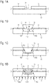
- a first substrate 1 with a first surface 11 and a second surface 12 opposite the first surface is provided (see Fig. Figure 1A ).
- the first substrate 1 is preferably in the form of a glass wafer.
- the first substrate 1 but z. B. also be a wafer made of silicon or quartz.
- the first surface 11 z. B. be a portion of a front wafer surface (wafer front). Accordingly, the second surface 12 may be a portion of a rear wafer surface (wafer rear side).
- a structured etching mask 2 which has at least one opening 20 is then produced on the first surface 11 .
- the etching mask 2 can be a hard mask, such as a chrome hard mask.
- the etching mask 2 can, for. B. be structured by means of known photolithographic methods. This is in the Figure 1A indicated by a structured layer of photoresist (resist) 3a.
- Figure 1B illustrates how a depression 110 is then produced in the first surface 11 by means of etching in the area of the opening 20 .
- an etchant such as. B. HF or KOH
- the material of the first substrate 1 z. B. glass
- the depression 110 thus produced can be a cavity or a channel in which or in which the following z. B. a metallic electrode is to be arranged.
- the depression 110 can be in the form of a channel with a depth T of up to a few hundred nanometers, approximately in the range from 0.05 ⁇ m to 5.0 ⁇ m, preferably in the range from 0.1 ⁇ m to 1.0 ⁇ m, such as 0 .5 ⁇ m.
- a width B of the channel 110 can be e.g. B. in the range of 1 micron to 5000 microns, preferably in the range of 1 micron to 500 microns, such as 100 microns.
- the etching mask 2 is initially not removed but left standing together with the edge sections 21 projecting laterally beyond the depression 110 .
- the subsequent process steps for generating an electrically conductive structure 4 in the depression 110 are self-aligned (English: "self-aligned"), so that, for example, some processes can be carried out on the entire wafer 1 without a targeted alignment of the already etched channel 110 (or if present on several such channels 110) must be carried out.
- the wafer surface 1 can be coated again with a photoresist 3, 3b, for example by means of spin coating.
- the photoresist 3, 3b covers the etching mask 2 and an area of a bottom 1101 of the depression 110 below the opening 20, as in FIG Figure 1C shown.
- the lateral etching radii 1102 below the protruding edge sections 21 of the etching mask 2 remain free of photoresist 3, 3b.
- Figure 1D 12 shows a further step in which the photoresist 3b is removed from the recess 110.
- FIG. This is accomplished in a self-aligned manner by exposure and subsequent development of the photoresist 3b in the recess 110.
- FIG. The (flood) exposure takes place through the second surface 12, ie from the rear. In Figure 1D this is indicated by vertical arrows L pointing upwards.
- the material of the first substrate 1 e.g. glass
- the material of the etching mask 2 e.g. chrome
- the exposed portion of the photoresist 3b is indicated by hatching.
- the photoresist 3 remains on the etching mask 2 .
- An electrically conductive material 4 is then deposited on the photoresist 3 covering the etching mask 2 and on a region of a bottom 1101 of the depression 110 below the opening 20, from which the photoresist 3b was previously removed.
- a metallic layer 4 e.g. gold
- the deposition is preferably carried out in such a way that a resulting layer thickness D of the electrically conductive material 4 in the recess 110 is not greater than a depth T of the recess 110 . This guarantees that the electrically conductive material 4 does not protrude from the recess 110 beyond the original first surface 11 and that subsequent direct bonding or other methods that require direct contact of the first surface 11 with another surface are not impeded.
- the lateral etching radii 1102 in the recess 110 are not coated during deposition, i.e. they remain free of electrically conductive material 4.
- a lift-off process removes the photoresist 3 (“resist strip”) together with the electrically conductive material 4 arranged thereon, so that the electrically conductive material 4 only remains in the depression 110 .
- the method also includes removing the etch mask 2, for example by a chromium etch, if the etch mask 2 consists of chromium.
- the photoresist 3 and the etching mask 2 can also be removed in one step. As in Figure 1G shown, what remains as a result is the metal 4 sunk into the depression 110 and, surrounding the depression 110, the now exposed first surface 11 of the first substrate 1.
- the first surface 11 is sufficiently clean and smooth for subsequent direct bonding.
- the first surface can have a surface roughness of less than 0.5 nm.
- Figure 1H 12 illustrates the result of a subsequent process step in which a second substrate 5 is attached to the first surface 11 by means of direct bonding.
- the second substrate 5 closes off the depression 110 at the top in the manner of a cover.
- the surface of the second substrate 5 used for direct bonding also has a depression (in Figure 1H not shown), this surface of the second substrate 5 being attached to the first surface 11 during direct bonding in such a way that the recess 110 of the first substrate 1 and the recess of the second substrate 5 face each other.
- the Figures 2A-D illustrate a further variant schematically and by way of example.
- the ones in the Figures 2A-B illustrated steps identical to those referred to Figures 1A-B explained. In this respect, reference is made to the above. Subsequently, however - in contrast to the embodiment according to Figures 1A-H (there in particular Figures 1C-E ) - be dispensed with the use of the photoresist 3.
- the electrically conductive material 4 for example gold, can then instead be deposited directly onto the etching mask 2 (e.g. made of chrome), as shown in FIG Figure 2C clarified.
- the etching mask 2 together with the conductive material 4 deposited thereon can then be removed by etching ( 2D ).
- the etching mask 2 itself (without photoresist) therefore has the function of a “lift-off barrier” for the electrically conductive material 4. It is advantageous for this if the layer thickness D of the electrically conductive material 4 is less than or equal to a layer thickness of Etching mask 2 is thus allowing etching of the etching mask 2 when the electrically conductive material 4 has already been deposited thereon. Such a lift-off process is further favored if there are many channels 110 which allow an etchant to locally penetrate under the electrically conductive layer 4 and thus attack the etching mask 2 .
Landscapes
- Chemical & Material Sciences (AREA)
- Health & Medical Sciences (AREA)
- Dispersion Chemistry (AREA)
- Analytical Chemistry (AREA)
- General Health & Medical Sciences (AREA)
- Hematology (AREA)
- Clinical Laboratory Science (AREA)
- Chemical Kinetics & Catalysis (AREA)
- Micromachines (AREA)
Description
- Diese Schrift betrifft Ausführungsformen von Verfahren zur Fertigung einer mikrofluidischen Vorrichtung.
- Mikrofluidische Vorrichtungen sind ausgebildet, Fluide, insbesondere Flüssigkeiten, in Strukturen, die wenigstens teilweise Abmessungen im Mikrometerbereich (wie von wenigen Mikrometern bis zu einigen hundert Mikrometer) haben, aufzunehmen und/oder zu leiten. Beispielsweise werden mikrofluidische Vorrichtungen in Form von sogenannten "Lab-on-a-Chip"-Systemen für medizintechnische oder allgemein biotechnologische Anwendungen eingesetzt. Derartige mikrofluidischen Vorrichtungen werden dementsprechend manchmal auch als Mikrofluidik-Chips bezeichnet. Es ist ferner bekannt, mikrofluidische Vorrichtungen in Form von sogenannten "Flow cells" z. B. für diagnostische Zwecke und speziell für die DNA-Sequenzierung zu verwenden.
- Üblicherweise umfasst eine solche mikrofluidische Vorrichtung ein erstes Substrat, z. B aus Glas, Quartz oder Silizium, mit einer Oberfläche, in welcher eine oder mehrere Vertiefungen vorgesehen sind, wobei die Vertiefung(en) ein oder mehrere Kavitäten und/oder Kanäle ausbilden. Dabei können in den Kavitäten und/oder Kanälen entsprechend der jeweiligen Funktion der mikrofluidischen Vorrichtung geeignete Chemikalien, Elektroden etc. angeordnet sein.
- Nach oben hin sind die Kavitäten und/oder Kanäle zumeist durch einen "Deckel" in Form eines zweiten Substrats abgeschlossen.
- Dabei sind im Rahmen der vorliegenden Beschreibung Angaben wie "nach oben", "oberer", "auf, "nach unten", "unterer" etc. lediglich relative Angaben, die bei einmal festgelegten Bezugssystem räumliche Beziehungen verschiedener Komponenten zueinander bezeichnen, aber keine absolute Orientierung im Raum festlegen.
- Der Abschluss der Kavitäten und/oder Kanäle durch das zweite Substrat muss insbesondere (wenigstens abschnittsweise) fluiddicht sein. In der Anwendung kann dann z. B. ein Analyt durch die Kanäle gedrückt und die entsprechende Analytik ausgeführt werden.
- Das erste Substrat und/oder das zweite Substrat können in Form eines Wafers (z. B. aus Glas oder Silizium) bzw. als Teil eines solchen Wafers bereitgestellt sein. In diesem Fall können die beiden Wafer beispielsweise durch sogenanntes Waferbonden aufeinander geklebt werden, wodurch der Kanal in dem Fluidleitungsteil mittels des Verschlussteils nach oben verschlossen wird.
- Beispielsweise wird beim sogenannten Klebebonden mittels eines dünnen Klebstofffilms eine flächige Verbindung zwischen zwei Wafern (wie z. B. Glaswafern) geschaffen. Diese Form der Verbindungstechnik wird insbesondere bei Komponenten eingesetzt, die in nachfolgenden Prozessschritten keinen erhöhten Temperaturen ausgesetzt werden dürfen, z. B. weil bereits Metalle oder biologische Funktionsstrukturen vorhanden sind, welche kein höheres Temperaturbudget vertragen.
- Als Alternative zum Klebebonden ist ferner bekannt, eine Oberfläche des zweiten Substrats mittels Direktbonden (auf Englisch: "direct bonding" oder "fusion bonding") an der Oberfläche des zweiten Substrats zu befestigen. Ein solches Verfahren kommt ohne Klebstoff oder andere Zwischenschichten aus. Stattdessen beruht die Befestigung auf chemischen Bindungen zwischen den Oberflächen, wie z. B van der Waals-Kräften, Wasserstoffbindungen oder starken kovalenten Bindungen.
- Voraussetzung dafür ist, dass die beteiligten Oberflächen hinreichen sauber, flach, und glatt sind. Insbesondere dürfen die Oberflächen keine zu großen Partikel oder Vorsprünge aufweisen. Mit anderen Worten müssen die Oberflächen eine äußerst geringe Oberflächenrauheit, beispielsweise von weniger als 0,5 nm, aufweisen, um das Direktbonden zu ermöglichen. Jeder Partikel mit einem Partikeldurchmesser von 0,5 nm oder mehr kann zu kontaktfreien Stellen (auch als Fehlstellen oder "Voids" bezeichnet) zwischen den beteiligten Oberflächen führen, wobei ein Durchmesser der kontaktfreien Stellen üblicherweise um etwa einen Faktor 10.000 größer als der Partikeldurchmessers ist. So kann beispielsweise ein 100 nm Partikel mit einem Partikeldurchmesser von 100 nm zu einem Void mit Durchmesser von ca. 1 mm führen.
- Aufgrund der vorstehend beschriebenen hohen Anforderungen an die Eigenschaften der Substratoberflächen ist ein Direktbonden von Wafern, insbesondere Glaswafern, mit strukturierten Oberflächen am Bond-Interface im Allgemeinen nicht möglich. In solchen Fällen wird daher üblicherweise auf alternative Bond-Technologien, wie z. B. das vorstehend erwähnte Klebebonden, zurückgegriffen, die in der Lage sind, die Stufen der Strukturen zu begraben oder anderweitig zu verhindern, dass sich um die Strukturen herum Voids ausbilden.
- Bei mikrofluidischen Vorrichtungen werden jedoch mitunter elektrisch leitfähige Strukturen im Bereich einer Oberfläche des ersten Substrats funktional, z. B. als metallische Elektroden, benötigt. Es ist wünschenswert, dennoch ein Direktbonden mit der Oberfläche eines zweiten Substrats zu ermöglichen.
- Aus der
US 5,525,190 A ist ein Fertigungsverfahren für einen optischen Wellenleiter bekannt, bei welchem in einer Oberfläche eines Substrats ausgebildete Kanäle von Innen mit einer reflektierenden Metallschicht versehen werden. Dabei wird die Metallschicht zunächst ganzflächig auf die Oberfläche und sowie auf Kanalböden und -wände abgeschieden. Anschließend wird das abgeschiedene Metall von der Oberfläche abgeschliffen, sodass es nur in den Kanälen stehen bleibt und dementsprechend strukturiert wird. Eine derartige Vorgehensweise würde jedoch, wenn sie auf die Erzeugung metallischer Strukturen in mikrofluidischen Vorrichtungen übertragen würde, nicht ohne Weiteres zu einer hinreichend glatten Oberfläche führen, welche ein Direktbonden mit einem weiteres Substrat zulassen würde. Daher wären ggf. aufwendige Schleif- und/oder Polierprozesse nötig, um die Voraussetzungen für ein Direktbonden zu schaffen. - Weitere mikrofluidische Vorrichtungen sind aus der
US 6 180 536 B1 sowie aus derUS 8 563 325 B1 bekannt. - Die vorliegende Erfindung stellt sich die Aufgabe, ein möglichst kosteneffizientes Verfahren zur Fertigung einer mikrofluidischen Vorrichtung bereitzustellen, bei welchem elektrisch leitfähige Strukturen im Bereich einer Oberfläche eines ersten Substrats angeordnet werden. Dabei soll das Verfahren jedenfalls prinzipiell mit einem Direktbonden der Oberfläche an ein zweites Substrat vereinbar sein, d. h., es soll insbesondere zu einer hinreichend glatten Oberfläche führen können.
- Des Weiteren wird eine entsprechende mikrofluidische Vorrichtung vorgeschlagen, die mit einem solchen Verfahren fertigbar ist.
- Die vorliegende Erfindung ist durch den unabhängigen Anspruch 1 definiert. Merkmale einiger Ausführungsbeispiele sind in den Unteransprüchen angegeben. Die Merkmale der Unteransprüche können miteinander zur Ausbildung weiterer Ausführungsformen kombiniert werden, sofern nicht ausdrücklich etwas anderes angegeben ist.
- Gemäß einem ersten Aspekt wird ein Verfahren zur Fertigung einer mikrofluidischen Vorrichtung vorgeschlagen. Das Verfahren umfasst zunächst die folgenden Schritte: Bereitstellen eines ersten Substrats mit einer ersten Oberfläche und einer der ersten Oberfläche gegenüberliegenden zweiten Oberfläche; Erzeugen einer Ätzmaske auf der ersten Oberfläche, wobei die Ätzmaske eine Öffnung aufweist; Erzeugen, mittels einer Ätzung, einer Vertiefung in der ersten Oberfläche im Bereich der Öffnung. Dabei umfasst das Verfahren ferner das Abscheiden eines elektrisch leitfähigen Materials auf die Ätzmaske und/oder eine die Ätzmaske bedeckende Schicht sowie auf einen Bereich eines Bodens der Vertiefung unterhalb der Öffnung.
- Das Verfahren gemäß dem ersten Aspekt umfasst dabei vor dem Abscheiden des elektrisch leitfähigen Materials die folgenden Schritte: Auftragen eines Fotolacks auf die Ätzmaske und auf einen Bereich eines Bodens der Vertiefung unterhalb der Öffnung; und Entfernen des Fotolacks aus der Vertiefung. Das elektrisch leitfähige Material wird auf den die Ätzmaske bedeckenden Fotolack und auf einen Bereich eines Bodens der Vertiefung unterhalb der Öffnung abgeschieden. Dabei wird das elektrisch leitfähige Material insbesondere auf den Bereich des Bodens der Vertiefung abgeschieden, von welchem in dem vorherigen Verfahrensschritt der Fotolack entfernt worden ist.
- Bevorzugt wird die Ätzmaske beim Erzeugen der Vertiefung wenigstens teilweise seitlich unterätzt, sodass wenigstens ein seitlicher Randabschnitt der Ätzmaske über einen Rand der Vertiefung hinaus übersteht.
- Das erste Substrat liegt bevorzugt in Form eines Wafers, z. B. aus Glas, vor. Dabei kann die erste Oberfläche z. B. ein Abschnitt einer vorderseitigen Waferoberfläche (Wafervorderseite) sein. Die zweite Oberfläche kann dementsprechend ein Abschnitt einer rückseitigen Waferoberfläche (Waferrückseite) sein.
- Nicht Teil der Erfindung ist eine mikrofluidische Vorrichtung, welche mittels eines Verfahrens gemäß dem ersten Aspekt gefertigt worden ist.
- Nicht Teil der Erfindung ist eine mikrofluidische Vorrichtung umfassend ein erstes Substrat mit einem darin ausgebildeten Kanal, wobei in dem Kanal ein elektrisch leitfähiges Material angeordnet ist, und wobei ein Boden des Kanals in einem Querschnitt seitliche Rundungen, insbesondere in Form von Ätzradien, aufweist. Dabei ist der Kanal im Bereich der Rundungen frei von dem elektrisch leitfähigen Material.
- Beispielsweise kann eine derartige mikrofluidische Vorrichtung mittels eines Verfahrens gemäß dem ersten Aspekt gefertigt worden sein.
- Nachstehend wird auf alle vorstehend genannten Aspekte Bezug genommen werden.
- Die Erfindung löst die Aufgabe, indem passend zu den zu erzeugenden leitfähigen Strukturen eine oder mehrere Vertiefung(en), z. B. in Form eines oder mehrerer Kanäle, in das erste Substrat geätzt werden. Die dabei verwendete strukturierte Ätzmaske bleibt nach dem Ätzen des Kanals stehen. Hierdurch werden die nachfolgenden Prozessschritte zur Erzeugung der elektrisch leitfähigen Strukturen selbstausrichtend. Insbesondere können nachfolgende Beschichtungsprozesse ganzflächig auf einem Wafer ausgeführt werden, ohne dass eine gezielte Justierung bezüglich der geätzten Vertiefung(en) erfolgen muss.
- Das vorgeschlagene selbstausrichtende Verfahren ist sowohl robust als auch kosteneffizient. Ein weiterer wesentlicher Vorteil des vorgeschlagenen Verfahrens ist, dass auf diese Weise ein Direktbonden auch mit (in Vertiefungen versenkten) metallischen Elektroden am Bond-Interface möglich wird.
- Bei einer gefertigten mikrofluidischen Vorrichtung kann sich die Verwendung des selbstausrichtenden Verfahrens insbesondere am Fehlen von metallisch leitfähigem Material in den Ätzradien der isotrop geätzten Vertiefung(en) zeigen.
- Gemäß einer Ausführungsform umfasst das Entfernen des Fotolacks aus der Vertiefung eine Belichtung des Fotolacks in der Vertiefung. Dabei kann eine Belichtung durch die zweite Oberfläche hindurch, d.h. beispielsweise von der Waferrückseite her, erfolgen.
- Das erste Substrat ist dabei vorzugsweise für Licht, das für eine Belichtung des Fotolacks geeignet ist, transparent. So wird es ermöglicht, dass der Fotolack in der Vertiefung durch eine Flutbelichtung durch die zweite Oberfläche hindurch belichtet wird.
- Demgegenüber kann vorgesehen sein, dass die Ätzmaske für Licht, das für eine Belichtung des Fotolacks verwendet wird, intransparent ist. So wird bei einer Flutbelichtung durch die zweite Oberfläche hindurch der Fotolack auf der Ätzmaske nicht belichtet.
- Auf diese Weise kann durch eine Belichtung von der Rückseite her sowie eine anschließende Entwicklung der Fotolack gezielt aus der Vertiefung entfernt werden, wohingegen der Fotolack vorderseitig auf der Ätzmaske stehen bleibt.
- Gemäß einer vorteilhaften Ausführungsform wird bei der Abscheidung eine Schichtdicke des elektrisch leitfähigen Materials in der Vertiefung so gewählt, dass sie kleiner als eine Tiefe der Vertiefung ist. Dies erlaubt später ein Direktbonden der ersten Oberfläche mit der Oberfläche eines zweiten Substrats, ohne dass das elektrisch leitfähige Material im Weg steht.
- Gemäß einer bevorzugten Ausführungsform ist die Vertiefung ein Kanal mit einer Tiefe im Bereich von 0,01 µm bis 5,0 µm, bevorzugt im Bereich von 0,1 µm bis 1,0 µm, wie z.B. 0,5 µm.
- Alternativ oder zusätzlich kann vorgesehen sein, dass die Vertiefung ein Kanal mit einer Breite im Bereich von 1 µm bis 5000 µm, bevorzugt im Bereich von 1 µm bis 500 µm ist, wie z.B. 100 µm, ist.
- In einer Weiterbildung umfasst das vorgeschlagene Verfahren ferner das Entfernen der Ätzmaske. Dies kann je nach dem Material der Ätzmaske z.B. durch eine Ätzung bewerkstelligt werden. Wird für die Ätzmaske beispielsweise Chrom als Material verwendet, so kann die Ätzmaske mittels einer Chromätzung entfernt werden.
- Es kann ferner vorgesehen sein, dass die erste Oberfläche eine Oberflächenrauheit von weniger als 0,5 nm aufweist. Hierdurch wird ein zuverlässiges Direktbonden der ersten Oberfläche an eine Oberfläche eines zweiten Substrats, etwa in Form eines zweiten Wafers, möglich.
- Es liegt nämlich auch im Rahmen der Erfindung, dass in einem weiteren Verfahrensschritt ein zweites Substrat mittels Waferbonden, insbesondere Direktbonden, an der ersten Oberfläche befestigt werden kann.
- In einer Ausführungsvariante kann dabei eine Oberfläche des zweiten Substrats eine Vertiefung aufweisen, wobei die Oberfläche des zweiten Substrats derart an der ersten Oberfläche befestigt wird, dass die Vertiefung des ersten Substrats und die Vertiefung des zweiten Substrats einander gegenüberliegen. So kann beispielsweise, wenn eine versenkte Metallelektrode auf dem ersten Substrat und ein Mikrofluidikkanal auf dem zweiten Substrat untergebracht wird, ein direkter Kontakt zwischen einem Medium (Fluid) in dem Mikrofluidikkanal und der Metallelektrode hergestellt werden.
- Als Materialien für das erste Substrat und/oder das zweite Substrat kommen bevorzugt Glas, Quartz oder Silizium in Frage. Insbesondere Glaswafer eignen sich für die vorstehend erläuterte Herstellungsvariante einer mikrofluidischen Vorrichtung mittels Waferbonden.
- Auch eine mikrofluidische Vorrichtung kann insbesondere mittels eines Verfahrens entsprechend dem ersten Aspekt hergestellt worden sein. Dementsprechend sind die vorstehenden und nachfolgenden Erläuterungen mit Bezug auf das Verfahren gemäß dem ersten Aspekt analog auf die mikrofluidischen Vorrichtungen anwendbar - und umgekehrt.
- Weitere Einzelheiten und Vorteile der Erfindung werden bei der nachfolgenden Beschreibung einiger Ausführungsbeispiele anhand der Figuren deutlich werden.
- Es zeigen:
- Fig. 1A-H
- schematisch und exemplarisch verschiedene Schritte und Zwischenstadien bei einem Verfahren zur Fertigung einer mikrofluidischen Vorrichtung gemäß einem oder mehreren Ausführungsbeispielen; und
- Fig. 2A-D
- schematisch und exemplarisch verschiedene Schritte und Zwischenstadien bei einem Verfahren zur Fertigung einer mikrofluidischen Vorrichtung.
- Zunächst wird ein erstes Substrats 1 mit einer ersten Oberfläche 11 und einer der ersten Oberfläche gegenüberliegenden zweiten Oberfläche 12 bereitgestellt (s.
Fig. 1A ). - Das erste Substrat 1 liegt bevorzugt in Form eines Wafers aus Glas vor. In einer alternativen Ausführungsvariante kann das erste Substrat 1 aber z. B. auch ein Wafer aus Silizium oder Quartz sein.
- Dabei kann die erste Oberfläche 11 z. B. ein Abschnitt einer vorderseitigen Waferoberfläche (Wafervorderseite) sein. Die zweite Oberfläche 12 kann dementsprechend ein Abschnitt einer rückseitigen Waferoberfläche (Waferrückseite) sein.
- Auf der ersten Oberfläche 11 wird sodann eine strukturierte Ätzmaske 2 erzeugt, die wenigstens eine Öffnung 20 aufweist. Bei der Ätzmaske 2 kann es sich um eine Hartmaske, wie z.B. eine Hartmaske aus Chrom, handeln. Die Ätzmaske 2 kann z. B. mittels an sich bekannter fotolithographischer Verfahren strukturiert werden. Dies ist in der
Fig. 1A durch eine strukturierte Schicht aus Fotolack (Resist) 3a angedeutet. - Bei der in
Fig. 1A dargestellten Querschnittsansicht ist eine entsprechende strukturierte Ätzung des Materials der Ätzmaske 2, beispielsweise Chrom, bereits erfolgt, wodurch die Öffnung 20 erzeugt worden ist. -
Fig. 1B veranschaulicht, wie anschließend mittels einer Ätzung im Bereich der Öffnung 20 eine Vertiefung 110 in der ersten Oberfläche 11 erzeugt wird. Dabei wird mit einem Ätzmittel, wie z. B. HF oder KOH, das Material des ersten Substrats 1 (z. B. Glas) isotrop geätzt. - In der schematischen Querschnittsansicht gemäß
Fig. 1B ist gut erkennbar, dass dabei die Ätzmaske 2 teilweise seitlich unterätzt wird, sodass seitliche Randabschnitte 21 der Ätzmaske 2 über einen Rand der Vertiefung 110 überstehen. Ferner wird anhand derFig. 1B deutlich, dass ein Boden 1101 der Vertiefung 110 in einem Querschnitt seitliche Rundungen 1102 aufweist. Die seitlichen Rundungen 1102 sind Ätzradien, die bei der isotropen Ätzung entstehen. - Die so erzeugte Vertiefung 110 kann eine Kavität oder ein Kanal sein in welcher bzw. in welchem in der Folge z. B. eine metallische Elektrode angeordnet werden soll. Beispielsweise kann die Vertiefung 110 die Form eines Kanals mit einer Tiefe T von bis zu einigen hundert Nanometern haben, etwa im Bereich von 0,05 µm bis 5,0 µm, bevorzugt im Bereich von 0,1 µm bis 1,0 µm, wie z.B. 0,5 µm.. Eine Breite B des Kanals 110 kann z. B. im Bereich von 1 µm bis 5000 µm, bevorzugt im Bereich von 1 µm bis 500 µm, wie z.B. 100 µm, liegen.
- Nach dem Ätzvorgang wird die Ätzmaske 2 zunächst nicht entfernt, sondern mitsamt den seitlich über die Vertiefung 110 überstehenden Randabschnitte 21 stehen gelassen. Hierdurch werden die nachfolgenden Prozessschritte zur Erzeugung einer elektrisch leitenden Struktur 4 in der Vertiefung 110 selbstausrichtend (Englisch: "self-aligned"), sodass beispielsweise einige Prozesse auf dem gesamten Wafer 1 ausgeführt werden können, ohne dass eine gezielte Ausrichtung an dem bereits geätzten Kanal 110 (bzw. falls vorhanden an mehreren derartigen Kanälen 110) vorgenommen werden muss.
- Dies soll im Folgenden anhand der weiteren Figuren deutlich gemacht werden.
- So kann die Waferoberfläche 1 in einem nachfolgenden Schritt erneut mit einem Fotolack 3, 3b beschichtet werden, beispielsweise mittels Spin-Coating. Im Ergebnis dieses Schritts bedeckt der Fotolack 3, 3b die Ätzmaske 2 sowie einen Bereich eines Bodens 1101 der Vertiefung 110 unterhalb der Öffnung 20, wie in
Fig. 1C dargestellt. Die seitlichen Ätzradien 1102 unterhalb der überstehenden Randabschnitte 21 der Ätzmaske 2 bleiben hingegen von Fotolack 3, 3b frei. -
Fig. 1D zeigt einen weiteren Schritt, in welchem der Fotolacks 3b aus der Vertiefung 110 entfernt wird. Dies wird in selbstausrichtender Weise mittels einer Belichtung und einer anschließenden Entwicklung des Fotolacks 3b in der Vertiefung 110 bewerkstelligt. Dabei erfolgt die (Flut-)Belichtung durch die zweite Oberfläche 12 hindurch, d. h. von der Rückseite her. InFig. 1D ist dies durch vertikale Pfeile L, die nach oben weisen, angedeutet. - Da das Material des ersten Substrats 1 (z. B. Glas) das zur Belichtung des Fotolacks 3b verwendete Licht L transparent ist, das Material der Ätzmaske 2 (z. B. Chrom) hingegen für dieses Licht L intransparent ist, wird in selbstausrichtender Weise gezielt der Fotolack 3b aus der Vertiefung 110 entfernt. In
Fig. 1D ist der belichtete Abschnitt des Fotolacks 3b schraffiert kenntlich gemacht. Auf der Ätzmaske 2 bleibt der Fotolack 3 hingegen stehen. - Auf den die Ätzmaske 2 bedeckenden Fotolack 3 und auf einen Bereich eines Bodens 1101 der Vertiefung 110 unterhalb der Öffnung 20, von dem zuvor der Fotolack 3b entfernt wurde, wird sodann ein elektrisch leitfähigen Material 4 abgeschieden. Beispielsweise kann in diesem Schritt eine metallische Schicht 4 (z. B. Gold) ganzflächig auf dem Wafer 1 abgeschieden werden. Dies ist schematisch in
Fig. 1E veranschaulicht. - Die Abscheidung wird bevorzugt in der Weise ausgeführt, dass eine resultierende Schichtdicke D des elektrisch leitfähigen Materials 4 in der Vertiefung 110 nicht größer als eine Tiefe T der Vertiefung 110 ist. Dadurch wird garantiert, dass das elektrisch leitfähige Material 4 nicht aus der Vertiefung 110 über die ursprüngliche erste Oberfläche 11 hinaus übersteht und dass ein späteres Direktbonden oder andere Verfahren, die einen direkten Kontakt der ersten Oberfläche 11 mit einer anderen Oberfläche erfordern nicht behindert wird.
- Die seitlichen Ätzradien 1102 in der Vertiefung 110 werden bei der Abscheidung nicht beschichtet, d.h. sie bleiben frei von elektrisch leitfähigem Material 4.
- In einem weiteren Schritt, dessen Ergebnis in
Fig. 1F veranschaulicht ist, entfernt ein Lift-Off-Prozess den Fotolack 3 ("Resist Strip") samt dem darauf angeordneten elektrisch leitfähigen Material 4., sodass das elektrisch leitfähige Material 4 lediglich in der Vertiefung 110 stehen bleibt. - Das Verfahren umfasst ferner das Entfernen der Ätzmaske 2, beispielsweise durch eine Chromätzung, falls die Ätzmaske 2 aus Chrom besteht. Das Entfernen des Fotolacks 3 und der Ätzmaske 2 kann gemäß einer Variante auch in einem Schritt erfolgen. Wie in
Fig. 1G gezeigt, verbleibt somit im Ergebnis das in der Vertiefung 110 versenkte Metall 4 sowie, die Vertiefung 110 umgebend, die nun freiliegende erste Oberfläche 11 des ersten Substrats 1. - Die erste Oberfläche 11 ist dabei hinreichend sauber und glatt für ein anschließendes Direktbonden. So kann die erste Oberfläche nach dem Entfernen der Ätzmaske 2 beispielsweise eine Oberflächenrauheit von weniger als 0,5 nm aufweisen.
-
Fig. 1H veranschaulicht das Ergebnis eines anschließenden Prozessschritts, in welchem ein zweites Substrat 5 mittels Direktbonden an der ersten Oberfläche 11 befestigt wird. Das zweite Substrat 5 schließt die Vertiefung 110 nach Art eines Deckels nach oben hin ab. Damit zeigt dieFig. 1H einen Abschnitt einer Querschnittsansicht einer erfindungsgemäßen mikrofluidischen Vorrichtung 6. - Dabei kann vorgesehen sein, dass auch die beim Direktbonden verwendete Oberfläche des zweiten Substrats 5, eine Vertiefung aufweist (in
Fig. 1H nicht dargestellt), wobei diese Oberfläche des zweiten Substrats 5 beim Direktbonden derart an der ersten Oberfläche 11 befestigt wird, dass die Vertiefung 110 des ersten Substrats 1 und die Vertiefung des zweiten Substrats 5 einander gegenüberliegen. So kann, wenn die versenkte Metallelektrode 4 wie gezeigt auf dem ersten Substrat 1 und ein Mikrofluidikkanal auf dem zweiten Substrat 5 untergebracht wird, ein direkter Kontakt zwischen einem Medium (Fluid) in dem Mikrofluidikkanal und der Metallelektrode 4 hergestellt werden. - Die
Fig. 2A-D veranschaulichen schematisch und beispielhaft eine weitere Variante. Dabei sind die in denFig. 2A-B veranschaulichten Schritte identisch zu den mit Bezug aufFig. 1A-B erläuterten. Insoweit wird auf das Vorstehende verwiesen. Im Anschluss daran kann jedoch - im Unterschied zu dem Ausführungsbeispiel gemäßFig. 1A-H (dort insbesondereFig. 1C-E ) - auf die Verwendung des Fotolacks 3 verzichtet werden. Das Abscheiden des elektrisch leitfähigen Materials 4, beispielsweise Gold, kann dann demnach stattdessen direkt auf die Ätzmaske 2 (z. B. aus Chrom) erfolgen, wie inFig. 2C verdeutlicht. Anschließend kann die Ätzmaske 2 mitsamt dem darauf abgeschiedenen leitfähigen Material 4 mittels einer Ätzung entfernt werden (Fig. 2D ). - Die Ätzmaske 2 selbst (ohne Fotolack) hat bei dieser Variante demnach die Funktion einer "Lift-off-Barriere" für das elektrisch leitfähige Material 4. Hierfür ist es vorteilhaft, wenn die Schichtdicke D des elektrisch leitfähigen Materials 4 kleiner oder gleich einer Schichtdicke der Ätzmaske 2 ist und damit ein Ätzen der Ätzmaske 2 erlaubt, wenn das elektrisch leitfähige Material 4 bereits darauf abgeschieden ist. Begünstigt wird ein solcher Lift-off-Prozess ferner, wenn viele Kanäle 110 vorhanden sind, die ein lokales Unterwandern der elektrisch leitfähigen Schicht 4 durch ein Ätzmittel und damit einen Angriff auf die Ätzmaske 2 erlauben.
-
- 1
- Erstes Substrat
- 11
- Erste Oberfläche
- 110
- Vertiefung / Kanal
- 1101
- Boden
- 1102
- Rundungen
- 12
- Zweite Oberfläche
- 2
- Ätzmaske
- 20
- Öffnung
- 21
- Randabschnitte
- 3, 3a
- Fotolack
- 3b
- Belichteter Abschnitt
- 4
- Elektrisch leitfähiges Material
- 5
- Zweites Substrat
- 6
- Mikrofluidische Vorrichtung
- B
- Breite
- D
- Schichtdicke des elektrisch leitfähigen Materials
- L
- Licht
- T
- Tiefe
Claims (8)
- Verfahren zur Fertigung einer mikrofluidischen Vorrichtung (6), umfassend die folgenden Schritte:- Bereitstellen eines ersten Substrats (1) mit einer ersten Oberfläche (11) und einer der ersten Oberfläche (11) gegenüberliegenden zweiten Oberfläche (12);- Erzeugen einer Ätzmaske (2) auf der ersten Oberfläche (11), wobei die Ätzmaske (2) eine Öffnung (20) aufweist;- Erzeugen, mittels einer Ätzung, einer Vertiefung (110) in der ersten Oberfläche (11) im Bereich der Öffnung (20);- Abscheiden eines elektrisch leitfähigen Materials (4) auf die Ätzmaske (2) und/oder eine die Ätzmaske (2) bedeckende Schicht (3) sowie auf einen Bereich eines Bodens (1101) der Vertiefung (110) unterhalb der Öffnung (20),
dadurch gekennzeichnet, dass das Verfahren vor dem Abscheiden des elektrisch leitfähigen Materials (4) die folgenden Schritte umfasst:- Auftragen eines Fotolacks (3, 3b) auf die Ätzmaske (2) und auf einen Bereich des Bodens (1101) der Vertiefung (110) unterhalb der Öffnung (20);- Entfernen des Fotolacks (3b) aus der Vertiefung (110), wobei das elektrisch leitfähige Material (4) danach auf den die Ätzmaske (2) bedeckenden Fotolack (3) und auf den Bereich des Bodens (1101) der Vertiefung (110) unterhalb der Öffnung (20) abgeschieden wird; und wobeio das Entfernen des Fotolacks (3b) aus der Vertiefung (110) eine Belichtung des Fotolacks (3b) in der Vertiefung (110) umfasst, wobei die Belichtung durch die zweite Oberfläche (12) hindurch erfolgt;o das erste Substrat (1) für Licht (L), das für eine Belichtung des Fotolacks (3, 3b) geeignet ist, transparent ist; undo die Ätzmaske (2) für Licht (L), das für eine Belichtung des Fotolacks (3, 3b) geeignet ist, intransparent ist. - Verfahren nach Anspruch 1, dadurch gekennzeichnet, dass die Ätzmaske (2) beim Erzeugen der Vertiefung (110) wenigstens teilweise seitlich unterätzt wird, sodass wenigstens ein seitlicher Randabschnitt (21) der Ätzmaske (2) über einen Rand der Vertiefung (110) hinaus übersteht.
- Verfahren nach einem der vorstehenden Ansprüche, dadurch gekennzeichnet, dass das erste Substrat (1) aus Glas, Quartz oder Silizium besteht.
- Verfahren nach einem der vorstehenden Ansprüche, dadurch gekennzeichnet, dass das Verfahren ferner das Entfernen der Ätzmaske (2) umfasst.
- Verfahren nach Anspruch 4, dadurch gekennzeichnet, dass die erste Oberfläche (11) nach dem Entfernen der Ätzmaske (2) eine Oberflächenrauheit von weniger als 0,5 nm aufweist.
- Verfahren nach einem der vorstehenden Ansprüche, dadurch gekennzeichnet, dass eine Schichtdicke (D) des elektrisch leitfähigen Materials (4) in der Vertiefung (110) nicht größer als eine Tiefe (T) der Vertiefung (110) ist.
- Verfahren nach einem der vorstehenden Ansprüche, dadurch gekennzeichnet, dass ein zweites Substrat (5) mittels Waferbonden, insbesondere Direktbonden, an der ersten Oberfläche (11) befestigt wird.
- Verfahren nach einem der vorstehenden Ansprüche, dadurch gekennzeichnet, dass eine Oberfläche des zweiten Substrats (5), eine Vertiefung aufweist, wobei die Oberfläche des zweiten Substrats (5) derart an der ersten Oberfläche (11) befestigt wird, dass die Vertiefung (110) des ersten Substrats (1) und die Vertiefung des zweiten Substrats (5) einander gegenüberliegen.
Priority Applications (3)
| Application Number | Priority Date | Filing Date | Title |
|---|---|---|---|
| EP19210724.1A EP3825003B1 (de) | 2019-11-21 | 2019-11-21 | Verfahren zur fertigung einer mikrofluidischen vorrichtung |
| PL19210724.1T PL3825003T3 (pl) | 2019-11-21 | 2019-11-21 | Sposób wytwarzania urządzenia mikroprzepływowego |
| US17/098,470 US11607683B2 (en) | 2019-11-21 | 2020-11-16 | Microfluidic device and method for manufacturing a microfluidic device |
Applications Claiming Priority (1)
| Application Number | Priority Date | Filing Date | Title |
|---|---|---|---|
| EP19210724.1A EP3825003B1 (de) | 2019-11-21 | 2019-11-21 | Verfahren zur fertigung einer mikrofluidischen vorrichtung |
Publications (2)
| Publication Number | Publication Date |
|---|---|
| EP3825003A1 EP3825003A1 (de) | 2021-05-26 |
| EP3825003B1 true EP3825003B1 (de) | 2022-06-01 |
Family
ID=68653390
Family Applications (1)
| Application Number | Title | Priority Date | Filing Date |
|---|---|---|---|
| EP19210724.1A Active EP3825003B1 (de) | 2019-11-21 | 2019-11-21 | Verfahren zur fertigung einer mikrofluidischen vorrichtung |
Country Status (3)
| Country | Link |
|---|---|
| US (1) | US11607683B2 (de) |
| EP (1) | EP3825003B1 (de) |
| PL (1) | PL3825003T3 (de) |
Families Citing this family (2)
| Publication number | Priority date | Publication date | Assignee | Title |
|---|---|---|---|---|
| EP4102543A1 (de) * | 2021-06-09 | 2022-12-14 | IMEC vzw | Verfahren zur übertragung einer schicht auf ein substrat |
| US20260121390A1 (en) * | 2024-10-28 | 2026-04-30 | Adeia Semiconductor Bonding Technologies Inc. | Transparent electrically conductive layers for fluidic cavities |
Family Cites Families (7)
| Publication number | Priority date | Publication date | Assignee | Title |
|---|---|---|---|---|
| US5562838A (en) | 1993-03-29 | 1996-10-08 | Martin Marietta Corporation | Optical light pipe and microwave waveguide interconnects in multichip modules formed using adaptive lithography |
| US5554488A (en) * | 1994-07-28 | 1996-09-10 | Northern Telecom Limited | Semiconductor device structure and method of formation thereof |
| US6180536B1 (en) * | 1998-06-04 | 2001-01-30 | Cornell Research Foundation, Inc. | Suspended moving channels and channel actuators for microfluidic applications and method for making |
| US8563325B1 (en) * | 2009-09-29 | 2013-10-22 | Sandia Corporation | Coaxial microreactor for particle synthesis |
| GB2515571A (en) * | 2013-06-28 | 2014-12-31 | Ibm | Fabrication of microfluidic chips having electrodes level with microchannel walls |
| US9620373B1 (en) * | 2015-12-31 | 2017-04-11 | Globalfoundries Singaporepte. Ltd. | Methods for fabricating semiconductor or micromachined devices with metal structures and methods for forming self-aligned deep cavity metal structures |
| US9728444B2 (en) * | 2015-12-31 | 2017-08-08 | International Business Machines Corporation | Reactive ion etching assisted lift-off processes for fabricating thick metallization patterns with tight pitch |
-
2019
- 2019-11-21 EP EP19210724.1A patent/EP3825003B1/de active Active
- 2019-11-21 PL PL19210724.1T patent/PL3825003T3/pl unknown
-
2020
- 2020-11-16 US US17/098,470 patent/US11607683B2/en active Active
Also Published As
| Publication number | Publication date |
|---|---|
| US20210154660A1 (en) | 2021-05-27 |
| US11607683B2 (en) | 2023-03-21 |
| EP3825003A1 (de) | 2021-05-26 |
| PL3825003T3 (pl) | 2022-08-22 |
Similar Documents
| Publication | Publication Date | Title |
|---|---|---|
| DE112014001600B4 (de) | Herstellung von Mikrofluidchips, die Elektroden auf einer Höhe mit Mikrokanalwänden aufweisen | |
| DE102013200214A1 (de) | Nanoeinheiten, gebildet mit eingehängter Graphen-Membran | |
| EP2434993B1 (de) | Verfahren zur herstellung eines medizinischen funktionselements mit einer freitragenden gitterstruktur | |
| DE10352404A1 (de) | Matrixsubstrat für eine Flüssigkristallanzeigevorrichtung und Verfahren zu dessen Herstellung | |
| EP3825003A1 (de) | Mikrofluidische vorrichtung und verfahren zur fertigung einer mikrofluidischen vorrichtung | |
| WO2009013255A2 (de) | Verfahren zum uebertragen einer epitaxie-schicht von einer spender- auf eine systemscheibe der mikrosystemtechnik | |
| DE19637878C2 (de) | Mikroventil mit vorgespannter Ventilklappenstruktur | |
| DE112017007356T5 (de) | Hohle versiegelte Vorrichtung und Herstellungsverfahren dafür | |
| DE102010062009A1 (de) | Verfahren zum Herstellen von Schrägflächen in einem Substrat und Wafer mit Schrägfläche | |
| DE102017207111A1 (de) | Verfahren zum Herstellen eines mikromechanischen Inertialsensors | |
| EP1322947B1 (de) | Verfahren zum herstellen einer 3-d-mikrodurchflusszelle und 3-d-mikrodurchflusszelle | |
| DE102010043059A1 (de) | Imprinttemplate, Nanoimprintvorrichtung und Nanostrukturierungsverfahren | |
| EP3665122B1 (de) | Mikromechanische vorrichtung und entsprechendes herstellungsverfahren | |
| DE102008037947A1 (de) | Element-Wafer und Verfahren zu dessen Herstellung | |
| EP1422194A1 (de) | Verfahren zur Herstellung eines Werkzeugeinsatzes zum Spritzgiessen eines mikrostrukturierten Teils | |
| WO2019180031A1 (de) | Verfahren zur herstellung und verwendung eines substrats mit einer funktionalisierten oberfläche | |
| EP1391541A1 (de) | Verfahren zur Bildung einer Ausnehmung in der Oberfläche eines Werkstücks, insbesondere zur Herstellung von Mikroformen | |
| EP1588383B1 (de) | SONDE FüR EIN OPTISCHES NAHFELDMIKROSKOP UND VERFAHREN ZU DEREN HERSTELLUNG | |
| WO2020148367A1 (de) | Nanostempelverfahren und nanooptisches bauteil | |
| EP3983125A1 (de) | Fluidleitungsteil für eine mikrofluidische vorrichtung, mikrofluidische vorrichtung und verfahren zur fertigung einer mikrofluidischen vorrichtung | |
| DE102021210382A1 (de) | Mikromechanisches Drucksensorelement | |
| DE10104957A1 (de) | Verfahren zum Herstellen einer 3-D-Mikrodurchflusszelle und 3-D-Mikrodurchflusszelle | |
| DE102004033440A1 (de) | Mikrostrukturierte Vorrichtung und Verfahren zu ihrer Herstellung | |
| EP1390988A2 (de) | Verfahren zum Erzeugen von optisch transparenten Bereichen in einem Siliziumsubstrat | |
| DE10130218A1 (de) | Vorrichtung für ein Patch-Clamping von Vesikeln und Verfahren zu deren Herstellung |
Legal Events
| Date | Code | Title | Description |
|---|---|---|---|
| PUAI | Public reference made under article 153(3) epc to a published international application that has entered the european phase |
Free format text: ORIGINAL CODE: 0009012 |
|
| STAA | Information on the status of an ep patent application or granted ep patent |
Free format text: STATUS: THE APPLICATION HAS BEEN PUBLISHED |
|
| AK | Designated contracting states |
Kind code of ref document: A1 Designated state(s): AL AT BE BG CH CY CZ DE DK EE ES FI FR GB GR HR HU IE IS IT LI LT LU LV MC MK MT NL NO PL PT RO RS SE SI SK SM TR |
|
| STAA | Information on the status of an ep patent application or granted ep patent |
Free format text: STATUS: REQUEST FOR EXAMINATION WAS MADE |
|
| 17P | Request for examination filed |
Effective date: 20211112 |
|
| RBV | Designated contracting states (corrected) |
Designated state(s): AL AT BE BG CH CY CZ DE DK EE ES FI FR GB GR HR HU IE IS IT LI LT LU LV MC MK MT NL NO PL PT RO RS SE SI SK SM TR |
|
| RIC1 | Information provided on ipc code assigned before grant |
Ipc: B81C 1/00 20060101ALI20211126BHEP Ipc: H01L 21/02 20060101ALI20211126BHEP Ipc: B01L 3/00 20060101AFI20211126BHEP |
|
| GRAP | Despatch of communication of intention to grant a patent |
Free format text: ORIGINAL CODE: EPIDOSNIGR1 |
|
| STAA | Information on the status of an ep patent application or granted ep patent |
Free format text: STATUS: GRANT OF PATENT IS INTENDED |
|
| INTG | Intention to grant announced |
Effective date: 20220112 |
|
| GRAS | Grant fee paid |
Free format text: ORIGINAL CODE: EPIDOSNIGR3 |
|
| GRAA | (expected) grant |
Free format text: ORIGINAL CODE: 0009210 |
|
| STAA | Information on the status of an ep patent application or granted ep patent |
Free format text: STATUS: THE PATENT HAS BEEN GRANTED |
|
| AK | Designated contracting states |
Kind code of ref document: B1 Designated state(s): AL AT BE BG CH CY CZ DE DK EE ES FI FR GB GR HR HU IE IS IT LI LT LU LV MC MK MT NL NO PL PT RO RS SE SI SK SM TR |
|
| REG | Reference to a national code |
Ref country code: GB Ref legal event code: FG4D Free format text: NOT ENGLISH |
|
| REG | Reference to a national code |
Ref country code: AT Ref legal event code: REF Ref document number: 1495006 Country of ref document: AT Kind code of ref document: T Effective date: 20220615 Ref country code: CH Ref legal event code: EP Ref country code: DE Ref legal event code: R096 Ref document number: 502019004497 Country of ref document: DE |
|
| REG | Reference to a national code |
Ref country code: IE Ref legal event code: FG4D Free format text: LANGUAGE OF EP DOCUMENT: GERMAN |
|
| REG | Reference to a national code |
Ref country code: LT Ref legal event code: MG9D |
|
| REG | Reference to a national code |
Ref country code: NL Ref legal event code: MP Effective date: 20220601 |
|
| PG25 | Lapsed in a contracting state [announced via postgrant information from national office to epo] |
Ref country code: SE Free format text: LAPSE BECAUSE OF FAILURE TO SUBMIT A TRANSLATION OF THE DESCRIPTION OR TO PAY THE FEE WITHIN THE PRESCRIBED TIME-LIMIT Effective date: 20220601 Ref country code: NO Free format text: LAPSE BECAUSE OF FAILURE TO SUBMIT A TRANSLATION OF THE DESCRIPTION OR TO PAY THE FEE WITHIN THE PRESCRIBED TIME-LIMIT Effective date: 20220901 Ref country code: LT Free format text: LAPSE BECAUSE OF FAILURE TO SUBMIT A TRANSLATION OF THE DESCRIPTION OR TO PAY THE FEE WITHIN THE PRESCRIBED TIME-LIMIT Effective date: 20220601 Ref country code: HR Free format text: LAPSE BECAUSE OF FAILURE TO SUBMIT A TRANSLATION OF THE DESCRIPTION OR TO PAY THE FEE WITHIN THE PRESCRIBED TIME-LIMIT Effective date: 20220601 Ref country code: GR Free format text: LAPSE BECAUSE OF FAILURE TO SUBMIT A TRANSLATION OF THE DESCRIPTION OR TO PAY THE FEE WITHIN THE PRESCRIBED TIME-LIMIT Effective date: 20220902 Ref country code: FI Free format text: LAPSE BECAUSE OF FAILURE TO SUBMIT A TRANSLATION OF THE DESCRIPTION OR TO PAY THE FEE WITHIN THE PRESCRIBED TIME-LIMIT Effective date: 20220601 Ref country code: BG Free format text: LAPSE BECAUSE OF FAILURE TO SUBMIT A TRANSLATION OF THE DESCRIPTION OR TO PAY THE FEE WITHIN THE PRESCRIBED TIME-LIMIT Effective date: 20220901 |
|
| PG25 | Lapsed in a contracting state [announced via postgrant information from national office to epo] |
Ref country code: RS Free format text: LAPSE BECAUSE OF FAILURE TO SUBMIT A TRANSLATION OF THE DESCRIPTION OR TO PAY THE FEE WITHIN THE PRESCRIBED TIME-LIMIT Effective date: 20220601 Ref country code: LV Free format text: LAPSE BECAUSE OF FAILURE TO SUBMIT A TRANSLATION OF THE DESCRIPTION OR TO PAY THE FEE WITHIN THE PRESCRIBED TIME-LIMIT Effective date: 20220601 |
|
| PG25 | Lapsed in a contracting state [announced via postgrant information from national office to epo] |
Ref country code: NL Free format text: LAPSE BECAUSE OF FAILURE TO SUBMIT A TRANSLATION OF THE DESCRIPTION OR TO PAY THE FEE WITHIN THE PRESCRIBED TIME-LIMIT Effective date: 20220601 |
|
| PG25 | Lapsed in a contracting state [announced via postgrant information from national office to epo] |
Ref country code: SM Free format text: LAPSE BECAUSE OF FAILURE TO SUBMIT A TRANSLATION OF THE DESCRIPTION OR TO PAY THE FEE WITHIN THE PRESCRIBED TIME-LIMIT Effective date: 20220601 Ref country code: SK Free format text: LAPSE BECAUSE OF FAILURE TO SUBMIT A TRANSLATION OF THE DESCRIPTION OR TO PAY THE FEE WITHIN THE PRESCRIBED TIME-LIMIT Effective date: 20220601 Ref country code: RO Free format text: LAPSE BECAUSE OF FAILURE TO SUBMIT A TRANSLATION OF THE DESCRIPTION OR TO PAY THE FEE WITHIN THE PRESCRIBED TIME-LIMIT Effective date: 20220601 Ref country code: PT Free format text: LAPSE BECAUSE OF FAILURE TO SUBMIT A TRANSLATION OF THE DESCRIPTION OR TO PAY THE FEE WITHIN THE PRESCRIBED TIME-LIMIT Effective date: 20221003 Ref country code: ES Free format text: LAPSE BECAUSE OF FAILURE TO SUBMIT A TRANSLATION OF THE DESCRIPTION OR TO PAY THE FEE WITHIN THE PRESCRIBED TIME-LIMIT Effective date: 20220601 Ref country code: EE Free format text: LAPSE BECAUSE OF FAILURE TO SUBMIT A TRANSLATION OF THE DESCRIPTION OR TO PAY THE FEE WITHIN THE PRESCRIBED TIME-LIMIT Effective date: 20220601 Ref country code: CZ Free format text: LAPSE BECAUSE OF FAILURE TO SUBMIT A TRANSLATION OF THE DESCRIPTION OR TO PAY THE FEE WITHIN THE PRESCRIBED TIME-LIMIT Effective date: 20220601 |
|
| PG25 | Lapsed in a contracting state [announced via postgrant information from national office to epo] |
Ref country code: IS Free format text: LAPSE BECAUSE OF FAILURE TO SUBMIT A TRANSLATION OF THE DESCRIPTION OR TO PAY THE FEE WITHIN THE PRESCRIBED TIME-LIMIT Effective date: 20221001 |
|
| REG | Reference to a national code |
Ref country code: DE Ref legal event code: R097 Ref document number: 502019004497 Country of ref document: DE |
|
| PG25 | Lapsed in a contracting state [announced via postgrant information from national office to epo] |
Ref country code: AL Free format text: LAPSE BECAUSE OF FAILURE TO SUBMIT A TRANSLATION OF THE DESCRIPTION OR TO PAY THE FEE WITHIN THE PRESCRIBED TIME-LIMIT Effective date: 20220601 |
|
| PLBE | No opposition filed within time limit |
Free format text: ORIGINAL CODE: 0009261 |
|
| STAA | Information on the status of an ep patent application or granted ep patent |
Free format text: STATUS: NO OPPOSITION FILED WITHIN TIME LIMIT |
|
| PG25 | Lapsed in a contracting state [announced via postgrant information from national office to epo] |
Ref country code: DK Free format text: LAPSE BECAUSE OF FAILURE TO SUBMIT A TRANSLATION OF THE DESCRIPTION OR TO PAY THE FEE WITHIN THE PRESCRIBED TIME-LIMIT Effective date: 20220601 |
|
| 26N | No opposition filed |
Effective date: 20230302 |
|
| PG25 | Lapsed in a contracting state [announced via postgrant information from national office to epo] |
Ref country code: SI Free format text: LAPSE BECAUSE OF FAILURE TO SUBMIT A TRANSLATION OF THE DESCRIPTION OR TO PAY THE FEE WITHIN THE PRESCRIBED TIME-LIMIT Effective date: 20220601 |
|
| PG25 | Lapsed in a contracting state [announced via postgrant information from national office to epo] |
Ref country code: MC Free format text: LAPSE BECAUSE OF FAILURE TO SUBMIT A TRANSLATION OF THE DESCRIPTION OR TO PAY THE FEE WITHIN THE PRESCRIBED TIME-LIMIT Effective date: 20220601 |
|
| REG | Reference to a national code |
Ref country code: BE Ref legal event code: MM Effective date: 20221130 |
|
| PG25 | Lapsed in a contracting state [announced via postgrant information from national office to epo] |
Ref country code: LU Free format text: LAPSE BECAUSE OF NON-PAYMENT OF DUE FEES Effective date: 20221121 |
|
| PG25 | Lapsed in a contracting state [announced via postgrant information from national office to epo] |
Ref country code: IE Free format text: LAPSE BECAUSE OF NON-PAYMENT OF DUE FEES Effective date: 20221121 |
|
| PG25 | Lapsed in a contracting state [announced via postgrant information from national office to epo] |
Ref country code: FR Free format text: LAPSE BECAUSE OF NON-PAYMENT OF DUE FEES Effective date: 20221130 Ref country code: BE Free format text: LAPSE BECAUSE OF NON-PAYMENT OF DUE FEES Effective date: 20221130 |
|
| PG25 | Lapsed in a contracting state [announced via postgrant information from national office to epo] |
Ref country code: IT Free format text: LAPSE BECAUSE OF FAILURE TO SUBMIT A TRANSLATION OF THE DESCRIPTION OR TO PAY THE FEE WITHIN THE PRESCRIBED TIME-LIMIT Effective date: 20220601 |
|
| PG25 | Lapsed in a contracting state [announced via postgrant information from national office to epo] |
Ref country code: CY Free format text: LAPSE BECAUSE OF FAILURE TO SUBMIT A TRANSLATION OF THE DESCRIPTION OR TO PAY THE FEE WITHIN THE PRESCRIBED TIME-LIMIT Effective date: 20220601 |
|
| PG25 | Lapsed in a contracting state [announced via postgrant information from national office to epo] |
Ref country code: MK Free format text: LAPSE BECAUSE OF FAILURE TO SUBMIT A TRANSLATION OF THE DESCRIPTION OR TO PAY THE FEE WITHIN THE PRESCRIBED TIME-LIMIT Effective date: 20220601 Ref country code: HU Free format text: LAPSE BECAUSE OF FAILURE TO SUBMIT A TRANSLATION OF THE DESCRIPTION OR TO PAY THE FEE WITHIN THE PRESCRIBED TIME-LIMIT; INVALID AB INITIO Effective date: 20191121 |
|
| PG25 | Lapsed in a contracting state [announced via postgrant information from national office to epo] |
Ref country code: TR Free format text: LAPSE BECAUSE OF FAILURE TO SUBMIT A TRANSLATION OF THE DESCRIPTION OR TO PAY THE FEE WITHIN THE PRESCRIBED TIME-LIMIT Effective date: 20220601 |
|
| GBPC | Gb: european patent ceased through non-payment of renewal fee |
Effective date: 20231121 |
|
| PG25 | Lapsed in a contracting state [announced via postgrant information from national office to epo] |
Ref country code: MT Free format text: LAPSE BECAUSE OF FAILURE TO SUBMIT A TRANSLATION OF THE DESCRIPTION OR TO PAY THE FEE WITHIN THE PRESCRIBED TIME-LIMIT Effective date: 20220601 |
|
| PG25 | Lapsed in a contracting state [announced via postgrant information from national office to epo] |
Ref country code: GB Free format text: LAPSE BECAUSE OF NON-PAYMENT OF DUE FEES Effective date: 20231121 |
|
| PG25 | Lapsed in a contracting state [announced via postgrant information from national office to epo] |
Ref country code: GB Free format text: LAPSE BECAUSE OF NON-PAYMENT OF DUE FEES Effective date: 20231121 |
|
| PG25 | Lapsed in a contracting state [announced via postgrant information from national office to epo] |
Ref country code: BG Free format text: LAPSE BECAUSE OF FAILURE TO SUBMIT A TRANSLATION OF THE DESCRIPTION OR TO PAY THE FEE WITHIN THE PRESCRIBED TIME-LIMIT Effective date: 20220601 |
|
| PG25 | Lapsed in a contracting state [announced via postgrant information from national office to epo] |
Ref country code: BG Free format text: LAPSE BECAUSE OF FAILURE TO SUBMIT A TRANSLATION OF THE DESCRIPTION OR TO PAY THE FEE WITHIN THE PRESCRIBED TIME-LIMIT Effective date: 20220601 |
|
| REG | Reference to a national code |
Ref country code: CH Ref legal event code: U11 Free format text: ST27 STATUS EVENT CODE: U-0-0-U10-U11 (AS PROVIDED BY THE NATIONAL OFFICE) Effective date: 20251201 |
|
| PGFP | Annual fee paid to national office [announced via postgrant information from national office to epo] |
Ref country code: DE Payment date: 20251119 Year of fee payment: 7 |
|
| REG | Reference to a national code |
Ref country code: CH Ref legal event code: R17 Free format text: ST27 STATUS EVENT CODE: U-0-0-R10-R17 (AS PROVIDED BY THE NATIONAL OFFICE) Effective date: 20260108 |
|
| PG25 | Lapsed in a contracting state [announced via postgrant information from national office to epo] |
Ref country code: AT Free format text: LAPSE BECAUSE OF NON-PAYMENT OF DUE FEES Effective date: 20241121 |
|
| REG | Reference to a national code |
Ref country code: AT Ref legal event code: MM01 Ref document number: 1495006 Country of ref document: AT Kind code of ref document: T Effective date: 20241121 |
|
| PGFP | Annual fee paid to national office [announced via postgrant information from national office to epo] |
Ref country code: CH Payment date: 20251201 Year of fee payment: 7 |
|
| PGFP | Annual fee paid to national office [announced via postgrant information from national office to epo] |
Ref country code: PL Payment date: 20251114 Year of fee payment: 7 |
|
| PGFP | Annual fee paid to national office [announced via postgrant information from national office to epo] |
Ref country code: AT Payment date: 20260410 Year of fee payment: 5 |