EP3820035A1 - Power conversion device and control method for power conversion device - Google Patents
Power conversion device and control method for power conversion device Download PDFInfo
- Publication number
- EP3820035A1 EP3820035A1 EP19830317.4A EP19830317A EP3820035A1 EP 3820035 A1 EP3820035 A1 EP 3820035A1 EP 19830317 A EP19830317 A EP 19830317A EP 3820035 A1 EP3820035 A1 EP 3820035A1
- Authority
- EP
- European Patent Office
- Prior art keywords
- semiconductor switch
- conversion device
- power conversion
- antiparallel diode
- voltage
- Prior art date
- Legal status (The legal status is an assumption and is not a legal conclusion. Google has not performed a legal analysis and makes no representation as to the accuracy of the status listed.)
- Withdrawn
Links
Images






Classifications
-
- H—ELECTRICITY
- H02—GENERATION; CONVERSION OR DISTRIBUTION OF ELECTRIC POWER
- H02M—APPARATUS FOR CONVERSION BETWEEN AC AND AC, BETWEEN AC AND DC, OR BETWEEN DC AND DC, AND FOR USE WITH MAINS OR SIMILAR POWER SUPPLY SYSTEMS; CONVERSION OF DC OR AC INPUT POWER INTO SURGE OUTPUT POWER; CONTROL OR REGULATION THEREOF
- H02M3/00—Conversion of DC power input into DC power output
- H02M3/01—Resonant DC/DC converters
-
- H—ELECTRICITY
- H02—GENERATION; CONVERSION OR DISTRIBUTION OF ELECTRIC POWER
- H02M—APPARATUS FOR CONVERSION BETWEEN AC AND AC, BETWEEN AC AND DC, OR BETWEEN DC AND DC, AND FOR USE WITH MAINS OR SIMILAR POWER SUPPLY SYSTEMS; CONVERSION OF DC OR AC INPUT POWER INTO SURGE OUTPUT POWER; CONTROL OR REGULATION THEREOF
- H02M3/00—Conversion of DC power input into DC power output
- H02M3/02—Conversion of DC power input into DC power output without intermediate conversion into AC
- H02M3/04—Conversion of DC power input into DC power output without intermediate conversion into AC by static converters
- H02M3/10—Conversion of DC power input into DC power output without intermediate conversion into AC by static converters using discharge tubes with control electrode or semiconductor devices with control electrode
- H02M3/145—Conversion of DC power input into DC power output without intermediate conversion into AC by static converters using discharge tubes with control electrode or semiconductor devices with control electrode using devices of a triode or transistor type requiring continuous application of a control signal
- H02M3/155—Conversion of DC power input into DC power output without intermediate conversion into AC by static converters using discharge tubes with control electrode or semiconductor devices with control electrode using devices of a triode or transistor type requiring continuous application of a control signal using semiconductor devices only
- H02M3/156—Conversion of DC power input into DC power output without intermediate conversion into AC by static converters using discharge tubes with control electrode or semiconductor devices with control electrode using devices of a triode or transistor type requiring continuous application of a control signal using semiconductor devices only with automatic control of output voltage or current, e.g. switching regulators
-
- H—ELECTRICITY
- H02—GENERATION; CONVERSION OR DISTRIBUTION OF ELECTRIC POWER
- H02M—APPARATUS FOR CONVERSION BETWEEN AC AND AC, BETWEEN AC AND DC, OR BETWEEN DC AND DC, AND FOR USE WITH MAINS OR SIMILAR POWER SUPPLY SYSTEMS; CONVERSION OF DC OR AC INPUT POWER INTO SURGE OUTPUT POWER; CONTROL OR REGULATION THEREOF
- H02M3/00—Conversion of DC power input into DC power output
- H02M3/22—Conversion of DC power input into DC power output with intermediate conversion into AC
- H02M3/24—Conversion of DC power input into DC power output with intermediate conversion into AC by static converters
- H02M3/28—Conversion of DC power input into DC power output with intermediate conversion into AC by static converters using discharge tubes with control electrode or semiconductor devices with control electrode to produce the intermediate AC
- H02M3/325—Conversion of DC power input into DC power output with intermediate conversion into AC by static converters using discharge tubes with control electrode or semiconductor devices with control electrode to produce the intermediate AC using devices of a triode or a transistor type requiring continuous application of a control signal
- H02M3/335—Conversion of DC power input into DC power output with intermediate conversion into AC by static converters using discharge tubes with control electrode or semiconductor devices with control electrode to produce the intermediate AC using devices of a triode or a transistor type requiring continuous application of a control signal using semiconductor devices only
- H02M3/33507—Conversion of DC power input into DC power output with intermediate conversion into AC by static converters using discharge tubes with control electrode or semiconductor devices with control electrode to produce the intermediate AC using devices of a triode or a transistor type requiring continuous application of a control signal using semiconductor devices only with automatic control of the output voltage or current, e.g. flyback converters
-
- H—ELECTRICITY
- H02—GENERATION; CONVERSION OR DISTRIBUTION OF ELECTRIC POWER
- H02M—APPARATUS FOR CONVERSION BETWEEN AC AND AC, BETWEEN AC AND DC, OR BETWEEN DC AND DC, AND FOR USE WITH MAINS OR SIMILAR POWER SUPPLY SYSTEMS; CONVERSION OF DC OR AC INPUT POWER INTO SURGE OUTPUT POWER; CONTROL OR REGULATION THEREOF
- H02M1/00—Details of apparatus for conversion
- H02M1/0003—Details of control, feedback or regulation circuits
- H02M1/0009—Devices or circuits for detecting current in a converter
-
- H—ELECTRICITY
- H02—GENERATION; CONVERSION OR DISTRIBUTION OF ELECTRIC POWER
- H02M—APPARATUS FOR CONVERSION BETWEEN AC AND AC, BETWEEN AC AND DC, OR BETWEEN DC AND DC, AND FOR USE WITH MAINS OR SIMILAR POWER SUPPLY SYSTEMS; CONVERSION OF DC OR AC INPUT POWER INTO SURGE OUTPUT POWER; CONTROL OR REGULATION THEREOF
- H02M1/00—Details of apparatus for conversion
- H02M1/0048—Circuits or arrangements for reducing losses
- H02M1/0054—Transistor switching losses
- H02M1/0058—Transistor switching losses by employing soft switching techniques, i.e. commutation of transistors when applied voltage is zero or when current flow is zero
-
- Y—GENERAL TAGGING OF NEW TECHNOLOGICAL DEVELOPMENTS; GENERAL TAGGING OF CROSS-SECTIONAL TECHNOLOGIES SPANNING OVER SEVERAL SECTIONS OF THE IPC; TECHNICAL SUBJECTS COVERED BY FORMER USPC CROSS-REFERENCE ART COLLECTIONS [XRACs] AND DIGESTS
- Y02—TECHNOLOGIES OR APPLICATIONS FOR MITIGATION OR ADAPTATION AGAINST CLIMATE CHANGE
- Y02B—CLIMATE CHANGE MITIGATION TECHNOLOGIES RELATED TO BUILDINGS, e.g. HOUSING, HOUSE APPLIANCES OR RELATED END-USER APPLICATIONS
- Y02B70/00—Technologies for an efficient end-user side electric power management and consumption
- Y02B70/10—Technologies improving the efficiency by using switched-mode power supplies [SMPS], i.e. efficient power electronics conversion e.g. power factor correction or reduction of losses in power supplies or efficient standby modes
Definitions
- the present invention relates to a power conversion device and a control method for the power conversion device.
- a power conversion device which includes a semiconductor switch and an antiparallel diode in antiparallel connection to the semiconductor switch, and in which a voltage applied to both ends of the semiconductor switch is varied over time by resonance (for example, see Patent Document 1).
- Such a power conversion device implements ZVS in a relatively narrow operating area.
- Patent Document 1 Japanese Translation of PCT Application No. JP H06-505844
- the present invention has been devised in view of the problem, and an object of the present invention is to provide a technique capable of extending an operating range that implements ZVS for a power conversion device, which includes a semiconductor switch and an antiparallel diode in antiparallel connection to the semiconductor switch, and in which a voltage applied to both ends of the semiconductor switch is varied over time by resonance.
- a power conversion device which includes a semiconductor switch and an antiparallel diode in antiparallel connection to the semiconductor switch, and in which a voltage applied to both ends of the semiconductor switch is varied over time by resonance according to an aspect of the present invention, further includes: control means for turning on/off the semiconductor switch; and detecting means for detecting a physical quantity in correlation with a current passing through the antiparallel diode, wherein the control means turns off the semiconductor switch in each setting period, and the control means turns on the semiconductor switch, which has been turned off, at a time between when a current starts passing through the antiparallel diode and when the current passing through the antiparallel diode falls to "0", on the basis of a detection result of the physical quantity detected by the detecting means.
- the power conversion device instead of turning on/off the semiconductor switch with a fixed duty ratio like a conventional power conversion device, the power conversion device according to the aspect of the present invention turns on the semiconductor switch at a time between when a current starts passing through the antiparallel diode and when the current passing through the antiparallel diode falls to "0", on the basis of the detection result of the physical quantity detected by the detecting means for detecting the physical quantity in correlation with the current passing through the antiparallel diode.
- the voltage of the semiconductor switch is substantially "0" from the time when a current starts passing through the antiparallel diode to the time when the current passing through the antiparallel diode falls to "0".
- the power conversion device implements ZVS in an operating area where ZVS is not achieved by conventional control.
- the power conversion device can be implemented as various devices including an inverter (e.g., a class E inverter), an insulating DC/DC converter, and a non-insulated DC/DC converter with different specific configurations and uses.
- the detecting means of the power conversion device only needs to detect a physical quantity in correlation with a current passing through the antiparallel diode.
- the detecting means may be means for detecting the magnitude of a current passing through the antiparallel diode.
- the detecting means may be means for detecting a voltage to each of both ends of a resistor connected in series with the antiparallel diode and the semiconductor switch or means for detecting a voltage generated by a voltage across the antiparallel diode or the on resistance of the semiconductor switch.
- the semiconductor switch may be turned on at a time between when a current starts passing through the antiparallel diode and when the current passing through the antiparallel diode falls to "0".
- the control means of the power conversion device may turn on the semiconductor switch, which has been turned off, when a current starts passing through the antiparallel diode.
- a control method for a power conversion device which includes a semiconductor switch and an antiparallel diode in antiparallel connection to the semiconductor switch, and in which a voltage applied to both ends of the semiconductor switch is varied over time by resonance according to an aspect of the present invention, includes: turning off the semiconductor switch in each setting period; detecting a physical quantity in correlation with a current passing through the antiparallel diode; and turning on the semiconductor switch, which has been turned off, at a time between when a current starts passing through the antiparallel diode and when the current passing through the antiparallel diode falls to "0", on the basis of the detection result of the physical quantity.
- the control method for the power conversion device implements ZVS in an operating area where ZVS is not achieved by conventional control.
- the present invention can extend the operating area that implements ZVS for the power conversion device.
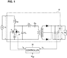
- Fig. 1 is an explanatory drawing illustrating a configuration example of the power conversion device according to the present embodiment.
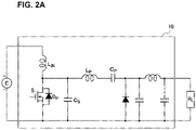
- Figs. 2A to 2C are explanatory drawings illustrating configuration examples of a resonant voltage-converter circuit 10 that is usable as a constituent element of the power conversion device according to the embodiment.
- the power conversion device includes the resonant voltage-converter circuit 10 and a controller 20.
- the resonant voltage-converter circuit 10 includes a semiconductor switch S and an antiparallel diode Dp in antiparallel connection to the semiconductor switch S, in which a voltage applied to both ends of the semiconductor switch S is varied over time by resonance.
- the antiparallel diode Dp is not necessarily provided as a device different from the semiconductor switch S. If the semiconductor switch S includes a parasitic diode (e.g., an FET), the parasitic diode may be provided as the antiparallel diode Dp.
- a parasitic diode e.g., an FET
- the resonant voltage-converter circuit 10 in Fig. 1 is an insulating DC/DC converter (a DC/DC converter with the primary side and the secondary side insulated from each other by a transformer).
- the resonant voltage-converter circuit 10 used as a constituent element of the power conversion device may be any circuit including the semiconductor switch S and the antiparallel diode Dp in antiparallel connection to the semiconductor switch S, in which a voltage applied to both ends of the semiconductor switch S is varied over time by resonance.
- the resonant voltage-converter circuit 10 may be a non-insulated DC/DC converter having a circuit configuration illustrated in Fig. 2A or 2B .
- the resonant voltage-converter circuit 10 may be an LLC resonant DC/DC converter.
- the resonant voltage-converter circuit 10 may be an inverter circuit having a circuit configuration illustrated in Fig. 2C .
- a voltage sensor 32 for measuring an output voltage V o of the resonant voltage-converter circuit 10 is attached to the resonant voltage-converter circuit 10.
- a detecting section 31 for detecting a current Is passing through the antiparallel diode Dp is attached to the resonant voltage-converter circuit 10.
- the detecting section 31 only needs to detect the presence or absence of current passing through the antiparallel diode D P .
- the detecting section 31 in Fig. 1 may be replaced with a detecting section for detecting a current value or a voltage value at another point of the resonant voltage-converter circuit 10.
- the detecting section 31 acts as a current sensor ( Fig. 1 ) for detecting the current I S .
- the controller 20 is a unit for controlling (ON/OFF) the semiconductor switch S so as to set the output voltage V o at a target voltage V tgt based on the current Is detected by the detecting section 31, the output voltage V o measured by the voltage sensor 32, and the target voltage V tgt .
- the controller 20 according to the present embodiment is a device including, as a main constituent element, a microcontroller for controlling a DC/DC converter.
- the controller 20 may have any hardware configuration as long as the resonant voltage-converter circuit 10 can be controlled as will be described later.
- the semiconductor switch S is turned on/off with a fixed duty ratio while a switching frequency is changed so as to set the output voltage V o to the target voltage
- conventional control the semiconductor switch S is turned on/off with a fixed duty ratio while a switching frequency is changed so as to set the output voltage V o to the target voltage
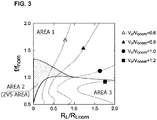
- FIG. 3 shows the relationship among V o /V onom , f/f nom , and R L /R Lnom when the resonant voltage-converter circuit 10 is controlled by the conventional control.
- V o , f, and R L denote an output voltage, a switching frequency, and a load R L , respectively, in the resonant voltage-converter circuit 10.
- V onom , f nom , and R Lnom denote a V o value, an f value, and an R L value, respectively, in an optimum state of the design.
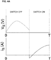
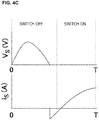
- "Area 1" and "area 3" in Fig. 3 are areas where a switching loss is generated in the absence of ZVS (zero volt switching). More specifically, as shown in Fig. 4A , area 1 is an area where the semiconductor switch S is turned on before a voltage Vs across the semiconductor switch S falls to "0". As shown in Fig. 4B , area 3 is an area where the semiconductor switch S is turned on after the voltage Vs at "0" starts rising again. Moreover, "area 2" in Fig. 3 is a ZVS area for ZVS, that is, an area where the semiconductor switch S is turned on when the voltage Vs is "0" as shown in Fig. 4C .
- the switching frequency f may not be uniquely determined (see dotted lines in Fig. 3 ) depending upon the combination of a resistance value R L and the output voltage V o , so that frequency control is difficult.
- the control on the resonant voltage-converter circuit 10 by the controller 20 is basically performed such that "the semiconductor switch S is turned on/off while a switching frequency is changed so as to set the output voltage V o to the target voltage V tgt ".
- the controller 20 monitors (stands by) the start of a current passing through the antiparallel diode D P based on the output of the detecting section 31 after the semiconductor switch S is turned off.
- the controller 20 turns on the semiconductor switch S when a current starts passing through the antiparallel diode D P .
- the semiconductor switch S may be turned on at any time between the time when current starts passing through the antiparallel diode D P and the time when the current passing through the antiparallel diode D P falls to "0".
- the semiconductor switch S may be turned on when, for example, the current I S is somewhat close to "0" after current starts passing through the antiparallel diode D P .
- the controller 20 of the power conversion device instead of turning on/off the semiconductor switch S with a fixed duty ratio, the controller 20 of the power conversion device according to the present embodiment turns on the semiconductor switch S at any time between the time when a current starts passing through the antiparallel diode D P and the time when the current passing through the antiparallel diode D P falls to "0".
- the control by the controller 20 enables ZVS in an operating area where ZVS is not achieved by the conventional control as indicated in the upper part of Fig. 5 .
- the operating area where the control by the controller 20 enables ZVS is "area 3" in Fig. 3 .
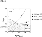
- the operating area where ZVS is enabled is extended by the range of area 3 from that of the conventional control as indicated in Fig. 6 .
- the power conversion device including the controller 20 of the present embodiment the operating area where ZVS is enabled is larger than that of the conventional control, and the power conversion device acts as a device capable of keeping ZVS even if disturbance (e.g., fluctuations in input voltage) occurs at a level where ZVS cannot be kept by a conventional device.
- the power conversion device according to the present embodiment also acts as a device provided without the need to limit an operating area even if frequency control is difficult (the switching frequency f is not uniquely determined).
- the detecting section 31 may be replaced with a detecting section 33 configured as illustrated in Fig. 7 , that is, the detecting section 33 that detects a forward voltage of the antiparallel diode D P , the forward voltage being generated when the current I S passes through the antiparallel diode D P .
- the detecting section 31 may be replaced with a detecting section 34 that detects a voltage across the semiconductor switch S and the antiparallel diode D P (a voltage generated by the on resistance of the semiconductor switch S).
- the controller 20 of the power conversion device may be modified to a device that performs the contents of control when predetermined conditions are satisfied and performs another control (for example, control for turning on/off the semiconductor switch S with a fixed duty ratio) when the predetermined conditions are not satisfied. Whether the predetermined conditions are satisfied or not is determined by, for example, an output voltage or an input voltage.
- the power conversion device may be modified to a device having a switching frequency that is controlled (changed) to set an output current or output power at a target value.
- an MOSFET is used as the semiconductor switch S.
- the semiconductor switch S may be a semiconductor switch (e.g., an IGBT) other than MOSFETs.
Landscapes
- Engineering & Computer Science (AREA)
- Power Engineering (AREA)
- Dc-Dc Converters (AREA)
- Inverter Devices (AREA)
Abstract
Description
- The present invention relates to a power conversion device and a control method for the power conversion device.
- As a power conversion device that implements ZVS (zero-voltage switching) with a simple circuit configuration, a power conversion device is known, which includes a semiconductor switch and an antiparallel diode in antiparallel connection to the semiconductor switch, and in which a voltage applied to both ends of the semiconductor switch is varied over time by resonance (for example, see Patent Document 1).
- Such a power conversion device implements ZVS in a relatively narrow operating area.
- [Patent Document 1] Japanese Translation of PCT Application No.
JP H06-505844 - The present invention has been devised in view of the problem, and an object of the present invention is to provide a technique capable of extending an operating range that implements ZVS for a power conversion device, which includes a semiconductor switch and an antiparallel diode in antiparallel connection to the semiconductor switch, and in which a voltage applied to both ends of the semiconductor switch is varied over time by resonance.
- In order to attain the object, a power conversion device, which includes a semiconductor switch and an antiparallel diode in antiparallel connection to the semiconductor switch, and in which a voltage applied to both ends of the semiconductor switch is varied over time by resonance according to an aspect of the present invention, further includes: control means for turning on/off the semiconductor switch; and detecting means for detecting a physical quantity in correlation with a current passing through the antiparallel diode, wherein the control means turns off the semiconductor switch in each setting period, and the control means turns on the semiconductor switch, which has been turned off, at a time between when a current starts passing through the antiparallel diode and when the current passing through the antiparallel diode falls to "0", on the basis of a detection result of the physical quantity detected by the detecting means.
- In other word, instead of turning on/off the semiconductor switch with a fixed duty ratio like a conventional power conversion device, the power conversion device according to the aspect of the present invention turns on the semiconductor switch at a time between when a current starts passing through the antiparallel diode and when the current passing through the antiparallel diode falls to "0", on the basis of the detection result of the physical quantity detected by the detecting means for detecting the physical quantity in correlation with the current passing through the antiparallel diode. The voltage of the semiconductor switch is substantially "0" from the time when a current starts passing through the antiparallel diode to the time when the current passing through the antiparallel diode falls to "0". Hence, the power conversion device according to the aspect of the present invention implements ZVS in an operating area where ZVS is not achieved by conventional control.
- The power conversion device can be implemented as various devices including an inverter (e.g., a class E inverter), an insulating DC/DC converter, and a non-insulated DC/DC converter with different specific configurations and uses. The detecting means of the power conversion device only needs to detect a physical quantity in correlation with a current passing through the antiparallel diode. Thus, the detecting means may be means for detecting the magnitude of a current passing through the antiparallel diode. The detecting means may be means for detecting a voltage to each of both ends of a resistor connected in series with the antiparallel diode and the semiconductor switch or means for detecting a voltage generated by a voltage across the antiparallel diode or the on resistance of the semiconductor switch. The semiconductor switch may be turned on at a time between when a current starts passing through the antiparallel diode and when the current passing through the antiparallel diode falls to "0". Thus, the control means of the power conversion device may turn on the semiconductor switch, which has been turned off, when a current starts passing through the antiparallel diode.
- A control method for a power conversion device, which includes a semiconductor switch and an antiparallel diode in antiparallel connection to the semiconductor switch, and in which a voltage applied to both ends of the semiconductor switch is varied over time by resonance according to an aspect of the present invention, includes: turning off the semiconductor switch in each setting period; detecting a physical quantity in correlation with a current passing through the antiparallel diode; and turning on the semiconductor switch, which has been turned off, at a time between when a current starts passing through the antiparallel diode and when the current passing through the antiparallel diode falls to "0", on the basis of the detection result of the physical quantity. Hence, the control method for the power conversion device implements ZVS in an operating area where ZVS is not achieved by conventional control.
- The present invention can extend the operating area that implements ZVS for the power conversion device.
-
-
Fig. 1 is an explanatory drawing illustrating a configuration example of a power conversion device according to an embodiment of the present invention; -
Fig. 2A is an explanatory drawing illustrating another configuration example of a resonant voltage-converter circuit; -
Fig. 2B is an explanatory drawing illustrating another configuration example of the resonant voltage-converter circuit; -
Fig. 2C is an explanatory drawing illustrating another configuration example of the resonant voltage-converter circuit; -
Fig. 3 is an explanatory drawing showing the relationship among Vo/Vonom, f/fnom, and RL/RLnom when the resonant voltage-converter circuit is controlled by conventional control; -
Fig. 4A is an explanatory drawing of the operations of the resonant voltage-converter circuit according to the conventional control; -
Fig. 4B is an explanatory drawing of the operations of the resonant voltage-converter circuit according to the conventional control; -
Fig. 4C is an explanatory drawing of the operations of the resonant voltage-converter circuit according to the conventional control; -
Fig. 5 is an explanatory drawing indicating the contents of control a controller; -
Fig. 6 is an explanatory drawing showing the relationship among Vo/Vonom, f/fnom, and RL/RLnom when the resonant voltage-converter circuit is controlled by the controller; -
Fig. 7 is an explanatory drawing illustrating a modification of the power conversion device according to the embodiment; and -
Fig. 8 is an explanatory drawing illustrating another modification of the power conversion device according to the embodiment. - An embodiment of the present invention will be described below with reference to the accompanying drawings.
- First, referring to
Figs. 1 and2A to 2C , the configuration of a power conversion device according to an embodiment of the present invention will be described below.Fig. 1 is an explanatory drawing illustrating a configuration example of the power conversion device according to the present embodiment.Figs. 2A to 2C are explanatory drawings illustrating configuration examples of a resonant voltage-converter circuit 10 that is usable as a constituent element of the power conversion device according to the embodiment. - As illustrated in
Fig. 1 , the power conversion device according to the present embodiment includes the resonant voltage-converter circuit 10 and acontroller 20. The resonant voltage-converter circuit 10 includes a semiconductor switch S and an antiparallel diode Dp in antiparallel connection to the semiconductor switch S, in which a voltage applied to both ends of the semiconductor switch S is varied over time by resonance. The antiparallel diode Dp is not necessarily provided as a device different from the semiconductor switch S. If the semiconductor switch S includes a parasitic diode (e.g., an FET), the parasitic diode may be provided as the antiparallel diode Dp. - The resonant voltage-
converter circuit 10 inFig. 1 is an insulating DC/DC converter (a DC/DC converter with the primary side and the secondary side insulated from each other by a transformer). The resonant voltage-converter circuit 10 used as a constituent element of the power conversion device may be any circuit including the semiconductor switch S and the antiparallel diode Dp in antiparallel connection to the semiconductor switch S, in which a voltage applied to both ends of the semiconductor switch S is varied over time by resonance. Thus, the resonant voltage-converter circuit 10 may be a non-insulated DC/DC converter having a circuit configuration illustrated inFig. 2A or2B . The resonant voltage-converter circuit 10 may be an LLC resonant DC/DC converter. Alternatively, the resonant voltage-converter circuit 10 may be an inverter circuit having a circuit configuration illustrated inFig. 2C . - As illustrated in
Fig. 1 , avoltage sensor 32 for measuring an output voltage Vo of the resonant voltage-converter circuit 10 is attached to the resonant voltage-converter circuit 10. Moreover, a detectingsection 31 for detecting a current Is passing through the antiparallel diode Dp is attached to the resonant voltage-converter circuit 10. The detectingsection 31 only needs to detect the presence or absence of current passing through the antiparallel diode DP. Thus, the detectingsection 31 inFig. 1 may be replaced with a detecting section for detecting a current value or a voltage value at another point of the resonant voltage-converter circuit 10. In the following description, the detectingsection 31 acts as a current sensor (Fig. 1 ) for detecting the current IS. - The
controller 20 is a unit for controlling (ON/OFF) the semiconductor switch S so as to set the output voltage Vo at a target voltage Vtgt based on the current Is detected by thedetecting section 31, the output voltage Vo measured by thevoltage sensor 32, and the target voltage Vtgt. Thecontroller 20 according to the present embodiment is a device including, as a main constituent element, a microcontroller for controlling a DC/DC converter. However, thecontroller 20 may have any hardware configuration as long as the resonant voltage-converter circuit 10 can be controlled as will be described later. - Before a description of the contents of control on the resonant voltage-converter circuit 10 (semiconductor switch S) by the
controller 20, conventional control performed on the resonant voltage-converter circuit 10 will be described below. - For the control of the resonant voltage-
converter circuit 10, the following control is typically used: "the semiconductor switch S is turned on/off with a fixed duty ratio while a switching frequency is changed so as to set the output voltage Vo to the target voltage" (hereinafter, will be denoted as conventional control). -
Fig. 3 shows the relationship among Vo/Vonom, f/fnom, and RL/RLnom when the resonant voltage-converter circuit 10 is controlled by the conventional control. Vo, f, and RL denote an output voltage, a switching frequency, and a load RL, respectively, in the resonant voltage-converter circuit 10. Furthermore, Vonom, fnom, and RLnom denote a Vo value, an f value, and an RL value, respectively, in an optimum state of the design. - "
Area 1" and "area 3" inFig. 3 are areas where a switching loss is generated in the absence of ZVS (zero volt switching). More specifically, as shown inFig. 4A ,area 1 is an area where the semiconductor switch S is turned on before a voltage Vs across the semiconductor switch S falls to "0". As shown inFig. 4B ,area 3 is an area where the semiconductor switch S is turned on after the voltage Vs at "0" starts rising again. Moreover, "area 2" inFig. 3 is a ZVS area for ZVS, that is, an area where the semiconductor switch S is turned on when the voltage Vs is "0" as shown inFig. 4C . - As is evident from
Fig. 3 , in the conventional control, ZVS cannot be performed at any switching frequency f when a Vo/Nonom value is 1.0 or larger, and even if the Vo/Nonom value is less than 1.0, ZVS can be performed only in an extremely narrow operating area. Moreover, in the conventional control, the switching frequency f may not be uniquely determined (see dotted lines inFig. 3 ) depending upon the combination of a resistance value RL and the output voltage Vo, so that frequency control is difficult. - The contents of control on the resonant voltage-
converter circuit 10 by thecontroller 20 will be described below. - The control on the resonant voltage-
converter circuit 10 by thecontroller 20 is basically performed such that "the semiconductor switch S is turned on/off while a switching frequency is changed so as to set the output voltage Vo to the target voltage Vtgt". Thecontroller 20 monitors (stands by) the start of a current passing through the antiparallel diode DP based on the output of the detectingsection 31 after the semiconductor switch S is turned off. Thecontroller 20 turns on the semiconductor switch S when a current starts passing through the antiparallel diode DP. The semiconductor switch S may be turned on at any time between the time when current starts passing through the antiparallel diode DP and the time when the current passing through the antiparallel diode DP falls to "0". Thus, the semiconductor switch S may be turned on when, for example, the current IS is somewhat close to "0" after current starts passing through the antiparallel diode DP. - Specifically, when the semiconductor switch S of the resonant voltage-converter circuit 10 (
Fig. 1 ) is turned off, a charging current passes through a capacitor Cs. Subsequently, the capacitor Cs is discharged by the resonance of a reactor Lp and a capacitor Cp. After the capacitor Cs is discharged, a current starts passing through the antiparallel diode Dp. The voltage Vs across the semiconductor switch S is kept at "0" until the current passing through the antiparallel diode Dp falls to "0" (seeFigs. 4B and4C ). Thus, ZVS can be achieved by turning on the semiconductor switch S at any time between the time when a current starts passing through the antiparallel diode DP and the time when the current passing through the antiparallel diode DP falls to "0". - As described above, instead of turning on/off the semiconductor switch S with a fixed duty ratio, the
controller 20 of the power conversion device according to the present embodiment turns on the semiconductor switch S at any time between the time when a current starts passing through the antiparallel diode DP and the time when the current passing through the antiparallel diode DP falls to "0". Hence, as indicated in the lower part ofFig. 5 , the control by thecontroller 20 enables ZVS in an operating area where ZVS is not achieved by the conventional control as indicated in the upper part ofFig. 5 . - The operating area where the control by the
controller 20 enables ZVS is "area 3" inFig. 3 . Hence, according to the control by thecontroller 20, the operating area where ZVS is enabled is extended by the range ofarea 3 from that of the conventional control as indicated inFig. 6 . Thus, according to the power conversion device including thecontroller 20 of the present embodiment, the operating area where ZVS is enabled is larger than that of the conventional control, and the power conversion device acts as a device capable of keeping ZVS even if disturbance (e.g., fluctuations in input voltage) occurs at a level where ZVS cannot be kept by a conventional device. - Furthermore, under the control of the
controller 20, a monotone increase can be provided between the switching frequency f and a load resistance RL (a characteristic of a monotone increase in f according to an increase in RL) in all ZVS areas corresponding toarea 2 + area 3 (seeFig. 6 ). Hence, the power conversion device according to the present embodiment also acts as a device provided without the need to limit an operating area even if frequency control is difficult (the switching frequency f is not uniquely determined). - The power conversion device according to the embodiment can be modified in various ways. For example, the detecting
section 31 may be replaced with a detectingsection 33 configured as illustrated inFig. 7 , that is, the detectingsection 33 that detects a forward voltage of the antiparallel diode DP, the forward voltage being generated when the current IS passes through the antiparallel diode DP. As indicated inFig. 8 , the detectingsection 31 may be replaced with a detectingsection 34 that detects a voltage across the semiconductor switch S and the antiparallel diode DP (a voltage generated by the on resistance of the semiconductor switch S). - The
controller 20 of the power conversion device may be modified to a device that performs the contents of control when predetermined conditions are satisfied and performs another control (for example, control for turning on/off the semiconductor switch S with a fixed duty ratio) when the predetermined conditions are not satisfied. Whether the predetermined conditions are satisfied or not is determined by, for example, an output voltage or an input voltage. - The power conversion device may be modified to a device having a switching frequency that is controlled (changed) to set an output current or output power at a target value. Moreover, in the resonant voltage-
converter circuit 10 illustrated inFigs. 1 and2A to 2C , an MOSFET is used as the semiconductor switch S. Naturally, the semiconductor switch S may be a semiconductor switch (e.g., an IGBT) other than MOSFETs. -
- (1) A power conversion device (10, 20), which includes a semiconductor switch (S) and an antiparallel diode (DP) in antiparallel connection to the semiconductor switch (S), and in which a voltage applied to both ends of the semiconductor switch (S) is varied over time by resonance,
- control means (20) for turning on/off the semiconductor switch (S); and
- detecting means (31;33;34) for detecting a physical quantity in correlation with a current passing through the antiparallel diode (DP), wherein
- the control means (20) turns off the semiconductor switch (S) in each setting period, and
- the control means (20) turns on the semiconductor switch (S), which has been turned off, at a time between when a current starts passing through the antiparallel diode (DP) and when the current passing through the antiparallel diode (DP) falls to "0", on the basis of a detection result of the physical quantity detected by the detecting means (31;33;34).
-
- 10
- Resonant voltage-converter circuit
- 20
- Controller
- 31, 33, 34
- Detecting section
- 32
- Voltage sensor
Claims (6)
- A power conversion device, which comprises a semiconductor switch and an antiparallel diode in antiparallel connection to the semiconductor switch, and in which a voltage applied to both ends of the semiconductor switch is varied over time by resonance, the power conversion device further comprising:control means for turning on/off the semiconductor switch; anddetecting means for detecting a physical quantity in correlation with a current passing through the antiparallel diode, whereinthe control meansturns off the semiconductor switch in each setting period, andturns on the semiconductor switch, which has been turned off, at a time between when a current starts passing through the antiparallel diode and when the current passing through the antiparallel diode falls to "0", on the basis of a detection result of the physical quantity detected by the detecting means.
- The power conversion device according to claim 1, wherein the control means changes the setting period so as to set any of an output voltage, an output current, and output power of the power conversion device at a target value.
- The power conversion device according to claim 1 or 2, wherein the detecting means detects a voltage at each of both ends of a resistor connected in series with the antiparallel diode and the semiconductor switch.
- The power conversion device according to claim 1 or 2, wherein the detecting means detects a voltage generated by an on resistance of the semiconductor switch.
- A control method for a power conversion device, which includes a semiconductor switch and an antiparallel diode in antiparallel connection to the semiconductor switch, and in which a voltage applied to both ends of the semiconductor switch is varied over time by resonance, the method comprising:turning off the semiconductor switch in each setting period;detecting a physical quantity in correlation with a current passing through the antiparallel diode; andturning on the semiconductor switch, which has been turned off, at a time between when a current starts passing through the antiparallel diode and when the current passing through the antiparallel diode falls to "0", on the basis of on a detection result of the physical quantity.
- The control method for controlling a power conversion device according to claim 5, further comprising changing the setting period so as to set any of an output voltage, an output current, and output power of the power conversion device at a target value.
Applications Claiming Priority (2)
| Application Number | Priority Date | Filing Date | Title |
|---|---|---|---|
| JP2018126796A JP7206452B2 (en) | 2018-07-03 | 2018-07-03 | POWER CONVERSION DEVICE AND CONTROL METHOD FOR POWER CONVERSION DEVICE |
| PCT/JP2019/026035 WO2020009052A1 (en) | 2018-07-03 | 2019-07-01 | Power conversion device and control method for power conversion device |
Publications (2)
| Publication Number | Publication Date |
|---|---|
| EP3820035A1 true EP3820035A1 (en) | 2021-05-12 |
| EP3820035A4 EP3820035A4 (en) | 2022-03-23 |
Family
ID=69059681
Family Applications (1)
| Application Number | Title | Priority Date | Filing Date |
|---|---|---|---|
| EP19830317.4A Withdrawn EP3820035A4 (en) | 2018-07-03 | 2019-07-01 | POWER CONVERTERS AND CONTROL METHODS FOR POWER CONVERTERS |
Country Status (4)
| Country | Link |
|---|---|
| EP (1) | EP3820035A4 (en) |
| JP (1) | JP7206452B2 (en) |
| CN (1) | CN112368925B (en) |
| WO (1) | WO2020009052A1 (en) |
Cited By (1)
| Publication number | Priority date | Publication date | Assignee | Title |
|---|---|---|---|---|
| EP4485785A4 (en) * | 2022-02-22 | 2025-03-26 | Nissan Motor Co., Ltd. | Electric-power conversion method and electric-power conversion device |
Families Citing this family (2)
| Publication number | Priority date | Publication date | Assignee | Title |
|---|---|---|---|---|
| JP7664086B2 (en) * | 2021-05-28 | 2025-04-17 | 日産自動車株式会社 | Method for controlling power converter and power converter |
| JP7811722B2 (en) * | 2022-06-30 | 2026-02-06 | パナソニックIpマネジメント株式会社 | Converter Circuit |
Family Cites Families (14)
| Publication number | Priority date | Publication date | Assignee | Title |
|---|---|---|---|---|
| NL8601798A (en) * | 1986-07-10 | 1988-02-01 | Hollandse Signaalapparaten Bv | ENERGY CONVERTER. |
| WO1992014300A1 (en) | 1991-02-04 | 1992-08-20 | Advanced Energy Industries, Inc. | High power switch-mode radio frequency amplifier method and apparatus |
| JP3097315B2 (en) * | 1992-05-15 | 2000-10-10 | 株式会社村田製作所 | High voltage generation circuit |
| US5430633A (en) * | 1993-09-14 | 1995-07-04 | Astec International, Ltd. | Multi-resonant clamped flyback converter |
| JP3007527B2 (en) * | 1994-05-17 | 2000-02-07 | コーセル株式会社 | Switching regulator |
| JP3402966B2 (en) * | 1996-11-15 | 2003-05-06 | 松下電工株式会社 | Power supply |
| JP2000324813A (en) * | 1999-05-07 | 2000-11-24 | Canon Inc | Power supply device and switching control method |
| CN100399688C (en) * | 2004-08-20 | 2008-07-02 | 艾默生网络能源有限公司 | Conversion soft switch circuit |
| JP5170117B2 (en) | 2010-01-18 | 2013-03-27 | 株式会社村田製作所 | Switching control circuit and switching power supply device |
| JP5488161B2 (en) * | 2010-04-23 | 2014-05-14 | 富士電機株式会社 | Power converter |
| JP2013027145A (en) | 2011-07-21 | 2013-02-04 | Sanken Electric Co Ltd | Switching power supply unit |
| JP6032908B2 (en) | 2012-03-21 | 2016-11-30 | キヤノン株式会社 | Power supply device and image forming apparatus having power supply device |
| JP2017508437A (en) | 2014-03-14 | 2017-03-23 | アヴォジー,インコーポレイテッド | Adaptive synchronous switching in resonant converters. |
| JP6390823B2 (en) | 2016-06-06 | 2018-09-19 | 株式会社村田製作所 | Switching power supply |
-
2018
- 2018-07-03 JP JP2018126796A patent/JP7206452B2/en active Active
-
2019
- 2019-07-01 EP EP19830317.4A patent/EP3820035A4/en not_active Withdrawn
- 2019-07-01 CN CN201980044266.7A patent/CN112368925B/en active Active
- 2019-07-01 WO PCT/JP2019/026035 patent/WO2020009052A1/en not_active Ceased
Cited By (1)
| Publication number | Priority date | Publication date | Assignee | Title |
|---|---|---|---|---|
| EP4485785A4 (en) * | 2022-02-22 | 2025-03-26 | Nissan Motor Co., Ltd. | Electric-power conversion method and electric-power conversion device |
Also Published As
| Publication number | Publication date |
|---|---|
| CN112368925A (en) | 2021-02-12 |
| CN112368925B (en) | 2024-11-29 |
| JP2020010430A (en) | 2020-01-16 |
| EP3820035A4 (en) | 2022-03-23 |
| JP7206452B2 (en) | 2023-01-18 |
| WO2020009052A1 (en) | 2020-01-09 |
Similar Documents
| Publication | Publication Date | Title |
|---|---|---|
| US10461658B2 (en) | Control device of a switching power supply | |
| US9093904B2 (en) | Resonant switching power supply device | |
| US9685876B2 (en) | Resonant converter with capacitive mode detection and associated detection method | |
| US9602010B2 (en) | Insulated DC power supply and a method of controlling same | |
| EP3414821B1 (en) | Dc/dc resonant converters and power factor correction using resonant converters, and corresponding control methods | |
| US6055170A (en) | Prediction methods and circuits for operating a transistor as a rectifier | |
| US20120026766A1 (en) | Control device of a switching power supply | |
| US20090201705A1 (en) | Energy converting apparatus, and semiconductor device and switching control method used therein | |
| US9337742B2 (en) | Switching power-supply device | |
| JP2011061913A (en) | Switching power supply device and semiconductor device therefor | |
| JP2020162326A (en) | Switching power supply | |
| KR101165386B1 (en) | Qusi-resonat converter and controlling method thereof | |
| CN112368925B (en) | Power conversion device and control method of power conversion device | |
| US7012821B1 (en) | Flyback converter with synchronous rectifier | |
| US7209372B2 (en) | Flyback converter with synchronous rectifier | |
| CN111193411A (en) | Synchronous rectifier tube control circuit and flyback voltage conversion circuit and control method | |
| CN114915190A (en) | Power supply control device and flyback converter | |
| US11616445B2 (en) | Method for driving a switch in a power converter, drive circuit and power converter | |
| JP2020188569A (en) | Switching circuit and gate drive circuit | |
| US10404170B2 (en) | Circuit of a power supply unit having a switching device | |
| CN111193410A (en) | Synchronous rectifier tube control circuit and its voltage conversion circuit and control method | |
| US10948525B2 (en) | Fault detection device and method for switch driving circuit, and electronic device | |
| US20040240243A1 (en) | Prediction methods and circuits for operating a transistor as a rectifier | |
| JP4720514B2 (en) | Current detection method in resonant converter | |
| US12573962B2 (en) | Isolated power supply control circuit and isolated power supply |
Legal Events
| Date | Code | Title | Description |
|---|---|---|---|
| STAA | Information on the status of an ep patent application or granted ep patent |
Free format text: STATUS: THE INTERNATIONAL PUBLICATION HAS BEEN MADE |
|
| PUAI | Public reference made under article 153(3) epc to a published international application that has entered the european phase |
Free format text: ORIGINAL CODE: 0009012 |
|
| STAA | Information on the status of an ep patent application or granted ep patent |
Free format text: STATUS: REQUEST FOR EXAMINATION WAS MADE |
|
| 17P | Request for examination filed |
Effective date: 20210107 |
|
| AK | Designated contracting states |
Kind code of ref document: A1 Designated state(s): AL AT BE BG CH CY CZ DE DK EE ES FI FR GB GR HR HU IE IS IT LI LT LU LV MC MK MT NL NO PL PT RO RS SE SI SK SM TR |
|
| DAV | Request for validation of the european patent (deleted) | ||
| DAX | Request for extension of the european patent (deleted) | ||
| REG | Reference to a national code |
Ref country code: DE Ref legal event code: R079 Free format text: PREVIOUS MAIN CLASS: H02M0003155000 Ipc: H02M0003000000 |
|
| A4 | Supplementary search report drawn up and despatched |
Effective date: 20220217 |
|
| RIC1 | Information provided on ipc code assigned before grant |
Ipc: H02M 3/335 20060101ALI20220211BHEP Ipc: H02M 3/156 20060101ALI20220211BHEP Ipc: H02M 3/00 20060101AFI20220211BHEP |
|
| STAA | Information on the status of an ep patent application or granted ep patent |
Free format text: STATUS: EXAMINATION IS IN PROGRESS |
|
| 17Q | First examination report despatched |
Effective date: 20230623 |
|
| STAA | Information on the status of an ep patent application or granted ep patent |
Free format text: STATUS: THE APPLICATION IS DEEMED TO BE WITHDRAWN |
|
| 18D | Application deemed to be withdrawn |
Effective date: 20250218 |