EP3817525A1 - Wiring board - Google Patents
Wiring board Download PDFInfo
- Publication number
- EP3817525A1 EP3817525A1 EP19826035.8A EP19826035A EP3817525A1 EP 3817525 A1 EP3817525 A1 EP 3817525A1 EP 19826035 A EP19826035 A EP 19826035A EP 3817525 A1 EP3817525 A1 EP 3817525A1
- Authority
- EP
- European Patent Office
- Prior art keywords
- conductor layer
- insulating layer
- layer
- wiring board
- build
- Prior art date
- Legal status (The legal status is an assumption and is not a legal conclusion. Google has not performed a legal analysis and makes no representation as to the accuracy of the status listed.)
- Withdrawn
Links
Images



Classifications
-
- H—ELECTRICITY
- H05—ELECTRIC TECHNIQUES NOT OTHERWISE PROVIDED FOR
- H05K—PRINTED CIRCUITS; CASINGS OR CONSTRUCTIONAL DETAILS OF ELECTRIC APPARATUS; MANUFACTURE OF ASSEMBLAGES OF ELECTRICAL COMPONENTS
- H05K3/00—Apparatus or processes for manufacturing printed circuits
- H05K3/30—Assembling printed circuits with electric components, e.g. with resistors
- H05K3/32—Assembling printed circuits with electric components, e.g. with resistors electrically connecting electric components or wires to printed circuits
- H05K3/34—Assembling printed circuits with electric components, e.g. with resistors electrically connecting electric components or wires to printed circuits by soldering
- H05K3/3452—Solder masks
-
- H—ELECTRICITY
- H10—SEMICONDUCTOR DEVICES; ELECTRIC SOLID-STATE DEVICES NOT OTHERWISE PROVIDED FOR
- H10W—GENERIC PACKAGES, INTERCONNECTIONS, CONNECTORS OR OTHER CONSTRUCTIONAL DETAILS OF DEVICES COVERED BY CLASS H10
- H10W70/00—Package substrates; Interposers; Redistribution layers [RDL]
- H10W70/60—Insulating or insulated package substrates; Interposers; Redistribution layers
- H10W70/67—Insulating or insulated package substrates; Interposers; Redistribution layers characterised by their insulating layers or insulating parts
- H10W70/68—Shapes or dispositions thereof
- H10W70/685—Shapes or dispositions thereof comprising multiple insulating layers
-
- H—ELECTRICITY
- H05—ELECTRIC TECHNIQUES NOT OTHERWISE PROVIDED FOR
- H05K—PRINTED CIRCUITS; CASINGS OR CONSTRUCTIONAL DETAILS OF ELECTRIC APPARATUS; MANUFACTURE OF ASSEMBLAGES OF ELECTRICAL COMPONENTS
- H05K1/00—Printed circuits
- H05K1/02—Details
- H05K1/09—Use of materials for the conductive, e.g. metallic pattern
-
- H—ELECTRICITY
- H05—ELECTRIC TECHNIQUES NOT OTHERWISE PROVIDED FOR
- H05K—PRINTED CIRCUITS; CASINGS OR CONSTRUCTIONAL DETAILS OF ELECTRIC APPARATUS; MANUFACTURE OF ASSEMBLAGES OF ELECTRICAL COMPONENTS
- H05K1/00—Printed circuits
- H05K1/02—Details
- H05K1/11—Printed elements for providing electric connections to or between printed circuits
- H05K1/115—Via connections; Lands around holes or via connections
-
- H—ELECTRICITY
- H05—ELECTRIC TECHNIQUES NOT OTHERWISE PROVIDED FOR
- H05K—PRINTED CIRCUITS; CASINGS OR CONSTRUCTIONAL DETAILS OF ELECTRIC APPARATUS; MANUFACTURE OF ASSEMBLAGES OF ELECTRICAL COMPONENTS
- H05K3/00—Apparatus or processes for manufacturing printed circuits
- H05K3/22—Secondary treatment of printed circuits
- H05K3/24—Reinforcing of the conductive pattern
- H05K3/244—Finish plating of conductors, especially of copper conductors, e.g. for pads or lands
-
- H—ELECTRICITY
- H05—ELECTRIC TECHNIQUES NOT OTHERWISE PROVIDED FOR
- H05K—PRINTED CIRCUITS; CASINGS OR CONSTRUCTIONAL DETAILS OF ELECTRIC APPARATUS; MANUFACTURE OF ASSEMBLAGES OF ELECTRICAL COMPONENTS
- H05K3/00—Apparatus or processes for manufacturing printed circuits
- H05K3/40—Forming printed elements for providing electric connections to or between printed circuits
- H05K3/42—Plated through-holes or plated via connections
- H05K3/429—Plated through-holes specially for multilayer circuits, e.g. having connections to inner circuit layers
-
- H—ELECTRICITY
- H05—ELECTRIC TECHNIQUES NOT OTHERWISE PROVIDED FOR
- H05K—PRINTED CIRCUITS; CASINGS OR CONSTRUCTIONAL DETAILS OF ELECTRIC APPARATUS; MANUFACTURE OF ASSEMBLAGES OF ELECTRICAL COMPONENTS
- H05K3/00—Apparatus or processes for manufacturing printed circuits
- H05K3/46—Manufacturing multilayer circuits
- H05K3/4644—Manufacturing multilayer circuits by building the multilayer layer by layer, i.e. build-up multilayer circuits
- H05K3/4652—Adding a circuit layer by laminating a metal foil or a preformed metal foil pattern
- H05K3/4655—Adding a circuit layer by laminating a metal foil or a preformed metal foil pattern by using a laminate characterized by the insulating layer
-
- H—ELECTRICITY
- H10—SEMICONDUCTOR DEVICES; ELECTRIC SOLID-STATE DEVICES NOT OTHERWISE PROVIDED FOR
- H10W—GENERIC PACKAGES, INTERCONNECTIONS, CONNECTORS OR OTHER CONSTRUCTIONAL DETAILS OF DEVICES COVERED BY CLASS H10
- H10W70/00—Package substrates; Interposers; Redistribution layers [RDL]
- H10W70/60—Insulating or insulated package substrates; Interposers; Redistribution layers
-
- H—ELECTRICITY
- H10—SEMICONDUCTOR DEVICES; ELECTRIC SOLID-STATE DEVICES NOT OTHERWISE PROVIDED FOR
- H10W—GENERIC PACKAGES, INTERCONNECTIONS, CONNECTORS OR OTHER CONSTRUCTIONAL DETAILS OF DEVICES COVERED BY CLASS H10
- H10W70/00—Package substrates; Interposers; Redistribution layers [RDL]
- H10W70/60—Insulating or insulated package substrates; Interposers; Redistribution layers
- H10W70/611—Insulating or insulated package substrates; Interposers; Redistribution layers for connecting multiple chips together
-
- H—ELECTRICITY
- H10—SEMICONDUCTOR DEVICES; ELECTRIC SOLID-STATE DEVICES NOT OTHERWISE PROVIDED FOR
- H10W—GENERIC PACKAGES, INTERCONNECTIONS, CONNECTORS OR OTHER CONSTRUCTIONAL DETAILS OF DEVICES COVERED BY CLASS H10
- H10W70/00—Package substrates; Interposers; Redistribution layers [RDL]
- H10W70/60—Insulating or insulated package substrates; Interposers; Redistribution layers
- H10W70/62—Insulating or insulated package substrates; Interposers; Redistribution layers characterised by their interconnections
- H10W70/63—Vias, e.g. via plugs
- H10W70/635—Through-vias
-
- H—ELECTRICITY
- H10—SEMICONDUCTOR DEVICES; ELECTRIC SOLID-STATE DEVICES NOT OTHERWISE PROVIDED FOR
- H10W—GENERIC PACKAGES, INTERCONNECTIONS, CONNECTORS OR OTHER CONSTRUCTIONAL DETAILS OF DEVICES COVERED BY CLASS H10
- H10W70/00—Package substrates; Interposers; Redistribution layers [RDL]
- H10W70/60—Insulating or insulated package substrates; Interposers; Redistribution layers
- H10W70/62—Insulating or insulated package substrates; Interposers; Redistribution layers characterised by their interconnections
- H10W70/66—Conductive materials thereof
-
- H—ELECTRICITY
- H05—ELECTRIC TECHNIQUES NOT OTHERWISE PROVIDED FOR
- H05K—PRINTED CIRCUITS; CASINGS OR CONSTRUCTIONAL DETAILS OF ELECTRIC APPARATUS; MANUFACTURE OF ASSEMBLAGES OF ELECTRICAL COMPONENTS
- H05K1/00—Printed circuits
- H05K1/02—Details
- H05K1/11—Printed elements for providing electric connections to or between printed circuits
- H05K1/111—Pads for surface mounting, e.g. lay-out
-
- H—ELECTRICITY
- H05—ELECTRIC TECHNIQUES NOT OTHERWISE PROVIDED FOR
- H05K—PRINTED CIRCUITS; CASINGS OR CONSTRUCTIONAL DETAILS OF ELECTRIC APPARATUS; MANUFACTURE OF ASSEMBLAGES OF ELECTRICAL COMPONENTS
- H05K2201/00—Indexing scheme relating to printed circuits covered by H05K1/00
- H05K2201/09—Shape and layout
- H05K2201/09209—Shape and layout details of conductors
- H05K2201/095—Conductive through-holes or vias
- H05K2201/09609—Via grid, i.e. two-dimensional array of vias or holes in a single plane
-
- H—ELECTRICITY
- H05—ELECTRIC TECHNIQUES NOT OTHERWISE PROVIDED FOR
- H05K—PRINTED CIRCUITS; CASINGS OR CONSTRUCTIONAL DETAILS OF ELECTRIC APPARATUS; MANUFACTURE OF ASSEMBLAGES OF ELECTRICAL COMPONENTS
- H05K3/00—Apparatus or processes for manufacturing printed circuits
- H05K3/46—Manufacturing multilayer circuits
- H05K3/4644—Manufacturing multilayer circuits by building the multilayer layer by layer, i.e. build-up multilayer circuits
-
- H—ELECTRICITY
- H10—SEMICONDUCTOR DEVICES; ELECTRIC SOLID-STATE DEVICES NOT OTHERWISE PROVIDED FOR
- H10W—GENERIC PACKAGES, INTERCONNECTIONS, CONNECTORS OR OTHER CONSTRUCTIONAL DETAILS OF DEVICES COVERED BY CLASS H10
- H10W90/00—Package configurations
- H10W90/701—Package configurations characterised by the relative positions of pads or connectors relative to package parts
- H10W90/721—Package configurations characterised by the relative positions of pads or connectors relative to package parts of bump connectors
- H10W90/724—Package configurations characterised by the relative positions of pads or connectors relative to package parts of bump connectors between a chip and a stacked insulating package substrate, interposer or RDL
Definitions
- the present disclosure relates to a wiring board.
- the wiring board has a plurality of electrodes located on the surface of the insulating layer. These electrodes are connected to the electrodes of the electronic components, for example, via solder. As the number of electrodes increases and the size of electrodes decreases due to the higher functionality of electronic components, the electrodes on the wiring board are also required to be downsized.
- Patent Document 1 Japanese Unexamined Patent Publication No. 2015-216344
- connection area between the electrodes and the insulating layer becomes smaller, and the connection strength between them may become smaller.
- cracks may occur between the electrodes and the insulating layer due to stress on the electrodes. This may result in an incomplete connection between the wiring board and the electronic components, which may prevent the electronic components from operating properly.
- a wiring board of the present disclosure comprises an insulating layer, a first conductor layer located on the surface of the insulating layer and containing any one of nickel and chromium, a metal belonging to group 4 of the periodic table; or a metal belonging to group 6 of the periodic table, a second conductor layer located inside the outer circumferential edge on the first conductor layer and containing copper, a third conductor layer located on the surface of the insulating layer in a state of covering the first conductor layer and the second conductor layer and containing nickel, and a fourth conductor layer located in a state of covering the third conductor layer and containing gold.
- the third conductor layer has an overhanging part extending outward from the outer circumferential edge of the first conductor layer, and the fourth conductor layer is located between the overhanging part and the insulating layer.
- the wiring board of the present disclosure it is possible to provide a wiring board that enables electronic components to operate stably.
- the wiring board 1 in one embodiment has a core insulating layer 2, a build-up insulating layer 3, a wiring conductor 4, an electrode 5, and a solder resist 6.
- the wiring board 1 is in the form of a flat plate with a square shape in plan view.
- One side of the wiring board 1 has a length of 5 to 80 mm and a thickness of 0.15 to 2.0 mm.
- a high functional integrated circuit S and a broadband memory M are mounted on the upper surface of the wiring board 1.
- the core insulating layer 2 includes an insulating material such as a reinforcing glass cloth impregnated with an epoxy resin or a bismaleimide triazine resin.
- the core insulating layer 2 has the function as a reinforcing support body in the wiring board 1.
- the thickness of the core insulating layer 2 is set, for example, from 50 to 1500 ⁇ m.
- the core insulating layer 2 is formed in a flat plate form by stacking a plurality of prepregs impregnated with a thermosetting resin such as an epoxy resin or a bismaleimide triazine resin in a reinforcing glass cloth and pressing under heating.
- the core insulating layer 2 has a plurality of through holes 7 penetrating from the upper surface to the lower surface.
- the wiring conductors 4 located on the upper and lower surfaces of the core insulating layer 2 are electrically connected to each other through the wiring conductors 4 in the through holes 7.
- the diameter of the through hole 7 is set between 40 and 500 ⁇ m, for example.
- the through hole 7 is formed by a processing such as drilling, laser machining, or blasting to the core insulating layer 2.
- the build-up insulating layer 3 is located on the upper surface and the lower surface of the core insulating layer 2. In the wiring board 1 of one embodiment, five layers of the build-up insulating layers 3 are located on the upper surface and the lower surface, respectively.
- the build-up insulating layer 3 has the function of securing an area for arranging the wiring conductor 4 on the upper and lower surfaces of the core insulating layer 2, as described below.
- the build-up insulating layer 3 covers the wiring conductor 4 and has the function of ensuring insulation between the wiring conductors 4 adjacent to each other.
- the build-up insulating layer 3 includes an insulating material, such as a polyimide resin, an epoxy resin or a bismaleimide triazine resin.
- the build-up insulating layer 3 may include glass fibers. However, with respect to the formation of the fine wiring conductor 4 and the formation of minute via hole 8 described below, it is more advantageous not to include glass fibers from the viewpoint of flatness or processability of the build-up insulating layer 3.
- the build-up insulating layer 3 contains insulating particles.
- the insulating particles include, for example, silica (SiO2) and alumina (Al2O3).
- the insulating particles have a spherical shape, for example, and the average particle size is set to, for example, 0.1 to 0.5 ⁇ m.
- the spherical shape is advantageous for containing a high density of insulating particles.
- the insulating particles have a role, in the build-up insulating layer 3, such as reducing the thermal expansion coefficient and suppressing the disconnection of the wiring conductor 4.
- the build-up insulating layer 3 is formed by attaching a film for the insulating layer in which insulating particles are dispersed in a thermosetting resin such as an epoxy resin, on the upper and lower surfaces of the core insulating layer 2 or on the surface of the build-up insulating layer 3 already formed, so as to cover the wiring conductors 4 under a vacuum, and thermally curing.
- a thermosetting resin such as an epoxy resin
- the build-up insulating layer 3 has a plurality of via holes 8 with the wiring conductors 4 at the bottom.
- the wiring conductors 4 located above and below through the build-up insulating layer 3 are electrically connected to each other through the wiring conductors 4 in the via holes 8.
- the diameter of the via hole 8 is set to, for example, 30 to 60 ⁇ m.
- the via hole 8 is formed, for example, by laser processing the build-up insulating layer 3. After laser processing, the inside of the via hole 8 can be cleaned to remove carbides and other foreign substances, thereby improving the connection strength between the via hole 8 and the wiring conductor 4.
- the wiring conductors 4 are located on the upper surface and the lower surface of the core insulating layer 2, in the through hole 7, on the upper surface or the lower surface of the build-up insulating layer 3, and in the via holes 8.
- the wiring conductor 4 constitutes the conductive path of the wiring board 1.
- the wiring conductor 4 includes a good conductive metal, such as an electroless copper-plated metal and an electrolytic copper-plated metal.
- the wiring conductor 4 is formed by a plating technique such as a semi-additive or subtractive method. Specifically, the wiring conductor 4 is formed by depositing copper-plated metal on the upper surface and the lower surface of the core insulating layer 2, inside the through hole 7, on the upper and lower surfaces of the build-up insulating layer 3, and in the via hole 8.
- the electrode 5 has a first electrode 5a and a second electrode 5b.
- the first electrode 5a is located on the upper surface of the uppermost build-up insulating layer 3.
- the second electrode 5b is located on the lower surface of the lowermost build-up insulating layer 3.
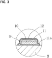
- the first electrode 5a is connected to the electrodes of the electronic components, for example, via solder. As shown in Fig. 3 , the first electrode 5a includes a first conductor layer 9, a second conductor layer 10, a third conductor layer 11, and a fourth conductor layer 12.
- the first conductor layer 9 is located on the surface of the build-up insulating layer 3.
- the first conductor layer 9 has the function as an underlying metal for the second conductor layer 10 and includes any one of nickel and chromium; a metal belonging to group 4 of the periodic table such as titanium; or a metal belonging to group 6 of the periodic table such as molybdenum.
- the first conductor layer 9 has excellent connectivity with the build-up insulating layer 3.
- the first conductor layer 9 is a circular shape in plan view, for example, with a diameter of 10 to 150 ⁇ m and a thickness of 10 to 100 nm.
- the first conductor layer 9 is formed, for example, by the sputtering method.
- the sputtering method is advantageous for improving the connection strength between the build-up insulating layer 3 and the first conductor layer 9 compared to the electroless plating method, because, for example, nickel and chromium are driven into the surface of the build-up insulating layer 3. This improves the connection strength between the first electrode 5a and the build-up insulating layer 3, which is particularly advantageous when the first electrode 5a is very small.
- the first conductor layer 9, other than the area where the first electrode 5a is located, is removed by etching to prevent a short circuit.
- the second conductor layer 10 is located on the upper surface of the first conductor layer 9.
- the second conductor layer 10 contains copper with excellent conductivity to lower the electrical resistance between the wiring board 1 and the electronic components.
- the second conductor layer 10 has a cylindrical shape, for example, with a diameter of 7 to 120 ⁇ m and a thickness of 5 to 30 ⁇ m.
- the second conductor layer 10 is located, for example, 1.5 to 15 ⁇ m inward from the outer circumferential edge on the first conductor layer 9.
- the second conductor layer 10 is formed, for example, as follows. First, a thin film layer of copper is formed by the sputtering method on the upper surface of the first conductor layer 9. The thickness of the thin film layer is set between 100 and 700 nm, for example. Next, a copper column in a cylindrical shape is formed on this thin film layer by an electrolytic plating method such as the semi-additive method. By forming the thin film layer of copper in advance on the upper surface of the first conductor layer 9, the electric resistance during electroplating is reduced, which is advantageous in terms of shortening the deposition time of the plating metal.
- the third conductor layer 11 is located on the surface of the build-up insulating layer 3, in a state of covering the first conductor layer 9 and the second conductor layer 10.
- the third conductor layer 11 has the function as a barrier metal to suppress metal diffusion between the second conductor layer 10 and the solder, and it contains nickel.
- the third conductor layer 11 may have a palladium film located on the outermost surface.
- the palladium film is more effective in suppressing metal diffusion than the third conductor layer 11 which contains nickel. Therefore, when the palladium film is located on the outermost surface of the third conductor layer 11, it is advantageous in terms of further suppressing metal diffusion between the second conductor layer 10 and the solder.
- the thickness of the palladium film is set between 10 and 50 nm, for example. This palladium film is formed, for example, by an electroless plating method.
- the third conductor layer 11 has an overhanging part 11a extending outward from the outer circumferential edge of the first conductor layer 9.
- the third conductor layer 11 in this example has the overhanging part 11a extending outward along the circumference of the first conductor layer 9, which is a circular shape in plan view.
- the overhanging part 11a is set, for example, to 3 to 5 ⁇ m in the vertical direction (perpendicular to the surface of the build-up insulating layer 3) and to 1 to 8 ⁇ m in the horizontal direction (horizontal to the surface of the build-up insulating layer 3).
- the thickness of the third conductor layer 11, other than the overhanging part 11a is set to 1 to 3 ⁇ m, for example.
- the third conductor layer 11 is formed, for example, by an electroless plating method. Compared with the electrolytic plating method, this electroless plating method is advantageous in terms of cost and reduction in the management burden of the equipment, as the plating equipment is simple. It is advantageous to improve the connection strength of the third conductor layer 11 as well as the first conductor layer 9 and the second conductor layer 10 if the surfaces of the first conductor layer 9 and the second conductor layer 10 are cleaned and the oxide film and the like are removed before the electroless plating process is performed.
- the fourth conductor layer 12 contains gold.
- the fourth conductor layer 12 is located in a state of covering the third conductor layer 11 exposed on the surface of the build-up insulating layer 3, as well as between the overhanging part 11a and the build-up insulating layer 3.
- the fourth conductor layer 12 covering the third conductor layer 11 described above has the function of suppressing corrosion of the third conductor layer 11.
- the thickness of the fourth conductor layer 12 covering the third conductor layer 11 is set to, for example, 50 to 500 nm.
- the fourth conductor layer 12 which is located between the overhanging part 11a and the build-up insulating layer 3 as described above, has a relaxation function to distribute stress when stress is applied between the overhanging part 11a (namely, the third conductor layer 11) and the build-up insulating layer 3.
- the first electrode 5a is connected to the electrodes of the electronic components via a solder and is therefore prone to be subjected to stress from the electronic components, for example, when the electronic components are mounted or operated. Therefore, the fourth conductor layer 12 is advantageous in relieving such stress.
- the fourth conductor layer 12 containing gold is more ductile than the third conductor layer 11 containing nickel. This makes it possible to distribute stress described above and to suppress the occurrence of cracks between the overhanging part 11a (namely, the third conductor layer 11) and the build-up insulating layer 3.
- the second electrode 5b is connected to the electrodes of the external board, for example, via a solder, and constitutes a conductive path between the wiring board 1 and the external board.
- the second electrode 5b includes a good conductive metal, such as an electroless copper-plated metal and an electrolytic copper-plated metal.
- the second electrode 5b is formed by depositing copper-plated metal on the lower surface of the lowermost build-up insulating layer 3 by using a plating technique such as a semi-additive or subtractive method.
- the solder resist 6 is located on the upper surface of the uppermost build-up insulating layer 3 and the lower surface of the lowermost build-up insulating layer 3.
- the solder resist 6 has an opening 6a to expose the first electrode 5a and an opening 6b to expose the second electrode 5b.
- the solder resist 6 is formed by affixing a film made of a photosensitive thermosetting resin, such as an acrylic-modified epoxy resin, to the surface of the build-up insulating layer 3, forming an opening 6a or 6b by exposure and development, and then thermally curing the film.
- the wiring board 1 of one embodiment of the present disclosure comprises the build-up insulating layer 3, the first conductor layer 9 located on the surface of the build-up insulating layer 3 and containing any one of nickel and chromium, the metal belonging to group 4 of the periodic table, or the metal belonging to group 6 of the periodic table, the second conductor layer 10 including copper and located inside the outer circumferential edge on the first conductor layer 9, the third conductor layer 11 including nickel and located on the surface of the build-up insulating layer 3 with the first conductor layer 9 and the second conductor layer 10 covered, and the fourth conductor layer 12 including gold and located in the state of covering the third conductor layer.
- the third conductor layer 11 has the overhanging part 11a extending outward from the outer circumferential edge of the first conductor layer 9, and the fourth conductor layer 12 is located between the overhanging part 11a and the build-up insulating layer 3.
- the fourth conductor layer 12 containing gold is superior in ductile to the third conductor layer 11 containing nickel. This makes it possible to distribute stress applied to the first electrode 5a and to suppress cracks between the overhanging part 11a (namely, the third conductor layer 11) and the build-up insulating layer 3.
- the wiring board 1 of the present disclosure it is possible to provide the wiring board 1 that has excellent connectivity between the wiring board 1 and the electronic components and enables the electronic components to operate stably. Furthermore, it is advantageous in that the fourth conductor layer 12 is located between the overhanging part 11a and the build-up insulating layer 3, which suppresses corrosion of the lower part of the overhanging part 11a.
- the first conductor layer 9 is located on the plane of the build-up insulating layer 3.
- the build-up insulating layer 3 has the via hole 8 with a via land 13 at the bottom thereof, and the first conductor layer 9 is located around the opening of the via hole 8, on the surface of the build-up insulating layer 3 inside the via hole 8, and on the upper surface of the via land 13.
- the wiring board 1 of the present disclosure can suppress the occurrence of cracks between the overhanging part 11a (namely, the third conductor layer 11) and the build-up insulating layer 3. As a result, it is advantageous in that the electrical connection between the first electrode 5a and the via land 13 (namely, the lower wiring conductor 4) is maintained in good condition.
- the surface roughness of the build-up insulating layer 3 where the overhanging part 11a is located may be greater than the surface roughness of the build-up insulating layer 3 where the first conductor layer 9 is located.
- the connection area between the fourth conductor layer 12 and the build-up insulating layer 3 is larger, thus improving the connection strength between the two. This is advantageous in terms of suppressing the occurrence of cracks between the overhanging part 11a (namely, the third conductor layer 11) and the build-up insulating layer 3.
- the surface roughness of the build-up insulating layer 3 where the overhanging part 11a is located for example, has an arithmetic mean roughness Ra of 0.05 to 0.2 ⁇ m
- the surface roughness of the build-up insulating layer 3 where the first conductor layer 9 is located has an arithmetic mean roughness Ra of 0.02 to 0.1 ⁇ m.
- the surface roughness of the latter is always smaller than the surface roughness of the former. It is more advantageous to have a smaller surface roughness of the build-up insulating layer 3 where the first conductor layer 9 is located, in terms of forming the first conductor layer 9 in a flat state.
- the surface roughness can be measured based on an image taken with a scanning electron microscope of a cross-section of the build-up insulating layer 3 in the area where, for example, the overhanging part 11a or the first conductor layer 9 is located.
- the area where they were located may be measured with a contact or non-contact surface roughness measuring device.
- the first electrode 5a is located only on the upper surface side of the wiring board 1.
- the first electrode may be located on both or either the upper and lower surfaces.
- the position of the first electrode 5a may be placed at an appropriate location corresponding to the position where the electronic components are mounted.
Landscapes
- Engineering & Computer Science (AREA)
- Microelectronics & Electronic Packaging (AREA)
- Manufacturing & Machinery (AREA)
- Production Of Multi-Layered Print Wiring Board (AREA)
- Electric Connection Of Electric Components To Printed Circuits (AREA)
Abstract
Description
- The present disclosure relates to a wiring board.
- Nowadays, a wiring board with highly functional electronic components are being developed. The wiring board has a plurality of electrodes located on the surface of the insulating layer. These electrodes are connected to the electrodes of the electronic components, for example, via solder. As the number of electrodes increases and the size of electrodes decreases due to the higher functionality of electronic components, the electrodes on the wiring board are also required to be downsized.
- Patent Document 1: Japanese Unexamined Patent Publication No.
2015-216344 - As described above, when the size of the electrodes on the wiring board is decreased, the connection area between the electrodes and the insulating layer becomes smaller, and the connection strength between them may become smaller. In such a case, when electronic components are mounted on the wiring board, for example, cracks may occur between the electrodes and the insulating layer due to stress on the electrodes. This may result in an incomplete connection between the wiring board and the electronic components, which may prevent the electronic components from operating properly.
- A wiring board of the present disclosure comprises an insulating layer, a first conductor layer located on the surface of the insulating layer and containing any one of nickel and chromium, a metal belonging to
group 4 of the periodic table; or a metal belonging togroup 6 of the periodic table, a second conductor layer located inside the outer circumferential edge on the first conductor layer and containing copper, a third conductor layer located on the surface of the insulating layer in a state of covering the first conductor layer and the second conductor layer and containing nickel, and a fourth conductor layer located in a state of covering the third conductor layer and containing gold. The third conductor layer has an overhanging part extending outward from the outer circumferential edge of the first conductor layer, and the fourth conductor layer is located between the overhanging part and the insulating layer. - According to the wiring board of the present disclosure, it is possible to provide a wiring board that enables electronic components to operate stably.
-
-
Fig. 1 is a schematic perspective view showing an embodiment example of the wiring board of the present disclosure. -
Fig. 2 is a schematic sectional view showing an embodiment example of the wiring board of the present disclosure. -
Fig. 3 is an enlarged sectional view showing a main part of an embodiment example of the wiring board of the present disclosure. -
Fig. 4 is an enlarged sectional view showing a main part of another embodiment example of the wiring board of the present disclosure. - Next, a wiring board according to one embodiment of the present disclosure will be described based on
Figs. 1 to 3 . Thewiring board 1 in one embodiment has acore insulating layer 2, a build-up insulating layer 3, awiring conductor 4, anelectrode 5, and a solder resist 6. Thewiring board 1 is in the form of a flat plate with a square shape in plan view. One side of thewiring board 1 has a length of 5 to 80 mm and a thickness of 0.15 to 2.0 mm. On the upper surface of thewiring board 1, for example, a high functional integrated circuit S and a broadband memory M are mounted. - The
core insulating layer 2 includes an insulating material such as a reinforcing glass cloth impregnated with an epoxy resin or a bismaleimide triazine resin. Thecore insulating layer 2 has the function as a reinforcing support body in thewiring board 1. The thickness of thecore insulating layer 2 is set, for example, from 50 to 1500 µm. The core insulating layer 2is formed in a flat plate form by stacking a plurality of prepregs impregnated with a thermosetting resin such as an epoxy resin or a bismaleimide triazine resin in a reinforcing glass cloth and pressing under heating. - The
core insulating layer 2 has a plurality of throughholes 7 penetrating from the upper surface to the lower surface. Thewiring conductors 4 located on the upper and lower surfaces of thecore insulating layer 2 are electrically connected to each other through thewiring conductors 4 in the throughholes 7. The diameter of thethrough hole 7 is set between 40 and 500 µm, for example. The throughhole 7 is formed by a processing such as drilling, laser machining, or blasting to thecore insulating layer 2. - The build-up insulating
layer 3 is located on the upper surface and the lower surface of thecore insulating layer 2. In thewiring board 1 of one embodiment, five layers of the build-up insulatinglayers 3 are located on the upper surface and the lower surface, respectively. The build-up insulatinglayer 3 has the function of securing an area for arranging thewiring conductor 4 on the upper and lower surfaces of thecore insulating layer 2, as described below. The build-up insulatinglayer 3 covers thewiring conductor 4 and has the function of ensuring insulation between thewiring conductors 4 adjacent to each other. - The build-up insulating
layer 3 includes an insulating material, such as a polyimide resin, an epoxy resin or a bismaleimide triazine resin. The build-up insulatinglayer 3 may include glass fibers. However, with respect to the formation of thefine wiring conductor 4 and the formation of minute viahole 8 described below, it is more advantageous not to include glass fibers from the viewpoint of flatness or processability of the build-up insulatinglayer 3. - The build-
up insulating layer 3 contains insulating particles. The insulating particles include, for example, silica (SiO2) and alumina (Al2O3). The insulating particles have a spherical shape, for example, and the average particle size is set to, for example, 0.1 to 0.5 µm. The spherical shape is advantageous for containing a high density of insulating particles. The insulating particles have a role, in the build-up insulating layer 3, such as reducing the thermal expansion coefficient and suppressing the disconnection of thewiring conductor 4. The build-up insulatinglayer 3 is formed by attaching a film for the insulating layer in which insulating particles are dispersed in a thermosetting resin such as an epoxy resin, on the upper and lower surfaces of thecore insulating layer 2 or on the surface of the build-up insulatinglayer 3 already formed, so as to cover thewiring conductors 4 under a vacuum, and thermally curing. - The build-
up insulating layer 3 has a plurality ofvia holes 8 with thewiring conductors 4 at the bottom. Thewiring conductors 4 located above and below through the build-up insulating layer 3 are electrically connected to each other through thewiring conductors 4 in thevia holes 8. The diameter of thevia hole 8 is set to, for example, 30 to 60 µm. Thevia hole 8 is formed, for example, by laser processing the build-up insulatinglayer 3. After laser processing, the inside of thevia hole 8 can be cleaned to remove carbides and other foreign substances, thereby improving the connection strength between thevia hole 8 and thewiring conductor 4. - The
wiring conductors 4 are located on the upper surface and the lower surface of thecore insulating layer 2, in the throughhole 7, on the upper surface or the lower surface of the build-up insulatinglayer 3, and in thevia holes 8. Thewiring conductor 4 constitutes the conductive path of thewiring board 1. Thewiring conductor 4 includes a good conductive metal, such as an electroless copper-plated metal and an electrolytic copper-plated metal. Thewiring conductor 4 is formed by a plating technique such as a semi-additive or subtractive method. Specifically, thewiring conductor 4 is formed by depositing copper-plated metal on the upper surface and the lower surface of thecore insulating layer 2, inside thethrough hole 7, on the upper and lower surfaces of the build-up insulatinglayer 3, and in thevia hole 8. - The
electrode 5 has afirst electrode 5a and asecond electrode 5b. Thefirst electrode 5a is located on the upper surface of the uppermost build-up insulatinglayer 3. Thesecond electrode 5b is located on the lower surface of the lowermost build-up insulatinglayer 3. Thefirst electrode 5a is connected to the electrodes of the electronic components, for example, via solder. As shown inFig. 3 , thefirst electrode 5a includes afirst conductor layer 9, asecond conductor layer 10, athird conductor layer 11, and afourth conductor layer 12. - The
first conductor layer 9 is located on the surface of the build-up insulatinglayer 3. Thefirst conductor layer 9 has the function as an underlying metal for thesecond conductor layer 10 and includes any one of nickel and chromium; a metal belonging togroup 4 of the periodic table such as titanium; or a metal belonging togroup 6 of the periodic table such as molybdenum. Thefirst conductor layer 9 has excellent connectivity with the build-up insulatinglayer 3. Thefirst conductor layer 9 is a circular shape in plan view, for example, with a diameter of 10 to 150 µm and a thickness of 10 to 100 nm. - The
first conductor layer 9 is formed, for example, by the sputtering method. The sputtering method is advantageous for improving the connection strength between the build-up insulatinglayer 3 and thefirst conductor layer 9 compared to the electroless plating method, because, for example, nickel and chromium are driven into the surface of the build-up insulatinglayer 3. This improves the connection strength between thefirst electrode 5a and the build-up insulatinglayer 3, which is particularly advantageous when thefirst electrode 5a is very small. Thefirst conductor layer 9, other than the area where thefirst electrode 5a is located, is removed by etching to prevent a short circuit. - The
second conductor layer 10 is located on the upper surface of thefirst conductor layer 9. Thesecond conductor layer 10 contains copper with excellent conductivity to lower the electrical resistance between thewiring board 1 and the electronic components. Thesecond conductor layer 10 has a cylindrical shape, for example, with a diameter of 7 to 120 µm and a thickness of 5 to 30 µm. Thesecond conductor layer 10 is located, for example, 1.5 to 15 µm inward from the outer circumferential edge on thefirst conductor layer 9. - The
second conductor layer 10 is formed, for example, as follows. First, a thin film layer of copper is formed by the sputtering method on the upper surface of thefirst conductor layer 9. The thickness of the thin film layer is set between 100 and 700 nm, for example. Next, a copper column in a cylindrical shape is formed on this thin film layer by an electrolytic plating method such as the semi-additive method. By forming the thin film layer of copper in advance on the upper surface of thefirst conductor layer 9, the electric resistance during electroplating is reduced, which is advantageous in terms of shortening the deposition time of the plating metal. - The
third conductor layer 11 is located on the surface of the build-up insulatinglayer 3, in a state of covering thefirst conductor layer 9 and thesecond conductor layer 10. Thethird conductor layer 11 has the function as a barrier metal to suppress metal diffusion between thesecond conductor layer 10 and the solder, and it contains nickel. - The
third conductor layer 11 may have a palladium film located on the outermost surface. The palladium film is more effective in suppressing metal diffusion than thethird conductor layer 11 which contains nickel. Therefore, when the palladium film is located on the outermost surface of thethird conductor layer 11, it is advantageous in terms of further suppressing metal diffusion between thesecond conductor layer 10 and the solder. The thickness of the palladium film is set between 10 and 50 nm, for example. This palladium film is formed, for example, by an electroless plating method. - The
third conductor layer 11 has an overhangingpart 11a extending outward from the outer circumferential edge of thefirst conductor layer 9. In other words, thethird conductor layer 11 in this example has the overhangingpart 11a extending outward along the circumference of thefirst conductor layer 9, which is a circular shape in plan view. The overhangingpart 11a is set, for example, to 3 to 5 µm in the vertical direction (perpendicular to the surface of the build-up insulating layer 3) and to 1 to 8 µm in the horizontal direction (horizontal to the surface of the build-up insulating layer 3). The thickness of thethird conductor layer 11, other than the overhangingpart 11a, is set to 1 to 3 µm, for example. - The
third conductor layer 11 is formed, for example, by an electroless plating method. Compared with the electrolytic plating method, this electroless plating method is advantageous in terms of cost and reduction in the management burden of the equipment, as the plating equipment is simple. It is advantageous to improve the connection strength of thethird conductor layer 11 as well as thefirst conductor layer 9 and thesecond conductor layer 10 if the surfaces of thefirst conductor layer 9 and thesecond conductor layer 10 are cleaned and the oxide film and the like are removed before the electroless plating process is performed. - The
fourth conductor layer 12 contains gold. Thefourth conductor layer 12 is located in a state of covering thethird conductor layer 11 exposed on the surface of the build-up insulatinglayer 3, as well as between the overhangingpart 11a and the build-up insulatinglayer 3. - The
fourth conductor layer 12 covering thethird conductor layer 11 described above has the function of suppressing corrosion of thethird conductor layer 11. The thickness of thefourth conductor layer 12 covering thethird conductor layer 11 is set to, for example, 50 to 500 nm. - The
fourth conductor layer 12, which is located between the overhangingpart 11a and the build-up insulatinglayer 3 as described above, has a relaxation function to distribute stress when stress is applied between the overhangingpart 11a (namely, the third conductor layer 11) and the build-up insulatinglayer 3. Thefirst electrode 5a is connected to the electrodes of the electronic components via a solder and is therefore prone to be subjected to stress from the electronic components, for example, when the electronic components are mounted or operated. Therefore, thefourth conductor layer 12 is advantageous in relieving such stress. - The
fourth conductor layer 12 containing gold is more ductile than thethird conductor layer 11 containing nickel. This makes it possible to distribute stress described above and to suppress the occurrence of cracks between the overhangingpart 11a (namely, the third conductor layer 11) and the build-up insulatinglayer 3. - The
second electrode 5b is connected to the electrodes of the external board, for example, via a solder, and constitutes a conductive path between thewiring board 1 and the external board. Thesecond electrode 5b includes a good conductive metal, such as an electroless copper-plated metal and an electrolytic copper-plated metal. Thesecond electrode 5b is formed by depositing copper-plated metal on the lower surface of the lowermost build-up insulatinglayer 3 by using a plating technique such as a semi-additive or subtractive method. - The solder resist 6 is located on the upper surface of the uppermost build-up insulating
layer 3 and the lower surface of the lowermost build-up insulatinglayer 3. The solder resist 6 has anopening 6a to expose thefirst electrode 5a and anopening 6b to expose thesecond electrode 5b. The solder resist 6 is formed by affixing a film made of a photosensitive thermosetting resin, such as an acrylic-modified epoxy resin, to the surface of the build-up insulatinglayer 3, forming anopening - As described above, the
wiring board 1 of one embodiment of the present disclosure comprises the build-up insulatinglayer 3, thefirst conductor layer 9 located on the surface of the build-up insulatinglayer 3 and containing any one of nickel and chromium, the metal belonging togroup 4 of the periodic table, or the metal belonging togroup 6 of the periodic table, thesecond conductor layer 10 including copper and located inside the outer circumferential edge on thefirst conductor layer 9, thethird conductor layer 11 including nickel and located on the surface of the build-up insulatinglayer 3 with thefirst conductor layer 9 and thesecond conductor layer 10 covered, and thefourth conductor layer 12 including gold and located in the state of covering the third conductor layer. - The
third conductor layer 11 has the overhangingpart 11a extending outward from the outer circumferential edge of thefirst conductor layer 9, and thefourth conductor layer 12 is located between the overhangingpart 11a and the build-up insulatinglayer 3. - The
fourth conductor layer 12 containing gold is superior in ductile to thethird conductor layer 11 containing nickel. This makes it possible to distribute stress applied to thefirst electrode 5a and to suppress cracks between the overhangingpart 11a (namely, the third conductor layer 11) and the build-up insulatinglayer 3. - As a result, according to the
wiring board 1 of the present disclosure, it is possible to provide thewiring board 1 that has excellent connectivity between thewiring board 1 and the electronic components and enables the electronic components to operate stably. Furthermore, it is advantageous in that thefourth conductor layer 12 is located between the overhangingpart 11a and the build-up insulatinglayer 3, which suppresses corrosion of the lower part of the overhangingpart 11a. - For example, it is also advantageous in terms of restraining the sealing resin from infiltrating between the overhanging
part 11a and the build-up insulatinglayer 3 and decreasing the connection strength between them, when the sealing resin is injected between them, after the electronic components are mounted on thewiring board 1. - The present disclosure is not limited to one example of the above-described embodiments, and various changes are possible to the extent that they do not depart from the gist of the present disclosure.
- In the
wiring board 1 according to one embodiment described above, for example, it is shown that thefirst conductor layer 9 is located on the plane of the build-up insulatinglayer 3. Apart from this case, as shown inFig. 4 , it may be a case that the build-up insulatinglayer 3 has the viahole 8 with a vialand 13 at the bottom thereof, and thefirst conductor layer 9 is located around the opening of the viahole 8, on the surface of the build-up insulatinglayer 3 inside the viahole 8, and on the upper surface of the vialand 13. - In such a case, the
wiring board 1 of the present disclosure can suppress the occurrence of cracks between the overhangingpart 11a (namely, the third conductor layer 11) and the build-up insulatinglayer 3. As a result, it is advantageous in that the electrical connection between thefirst electrode 5a and the via land 13 (namely, the lower wiring conductor 4) is maintained in good condition. - In plan view, the surface roughness of the build-up insulating
layer 3 where the overhangingpart 11a is located may be greater than the surface roughness of the build-up insulatinglayer 3 where thefirst conductor layer 9 is located. In this case, the connection area between thefourth conductor layer 12 and the build-up insulatinglayer 3 is larger, thus improving the connection strength between the two. This is advantageous in terms of suppressing the occurrence of cracks between the overhangingpart 11a (namely, the third conductor layer 11) and the build-up insulatinglayer 3. - In plan view, the surface roughness of the build-up insulating
layer 3 where the overhangingpart 11a is located, for example, has an arithmetic mean roughness Ra of 0.05 to 0.2 µm, and the surface roughness of the build-up insulatinglayer 3 where thefirst conductor layer 9 is located has an arithmetic mean roughness Ra of 0.02 to 0.1 µm. The surface roughness of the latter is always smaller than the surface roughness of the former. It is more advantageous to have a smaller surface roughness of the build-up insulatinglayer 3 where thefirst conductor layer 9 is located, in terms of forming thefirst conductor layer 9 in a flat state. - The surface roughness can be measured based on an image taken with a scanning electron microscope of a cross-section of the build-up insulating
layer 3 in the area where, for example, the overhangingpart 11a or thefirst conductor layer 9 is located. Alternatively, after removing the overhangingpart 11a or thefirst conductor layer 9 by etching, the area where they were located may be measured with a contact or non-contact surface roughness measuring device. - One example of the above-described embodiment shows the case that the
first electrode 5a is located only on the upper surface side of thewiring board 1. However, in the wiring board of the present disclosure, the first electrode may be located on both or either the upper and lower surfaces. The position of thefirst electrode 5a may be placed at an appropriate location corresponding to the position where the electronic components are mounted. -
- 1
- Wiring Board
- 3
- Build-up Insulating Layer
- 8
- Via Hole
- 9
- First Conductor Layer
- 10
- Second Conductor Layer
- 11
- Third Conductor Layer
- 11a
- Overhanging Part
- 12
- Fourth Conductor Layer
- 13
- Via Land
Claims (6)
- A wiring board comprising:an insulating layer,a first conductor layer located on the surface of the insulating layer, and containing any one of nickel and chromium, a metal belonging to group 4 of the periodic table, or a metal belonging to group 6 of the periodic table,a second conductor layer located inside of the outer circumferential edge of the first conductor layer, and containing copper,a third conductor layer located on the surface of the insulating layer in a state of covering the first conductor layer and the second conductor layer and containing nickel, anda fourth conductor layer located in a state of covering the third conductor layer, and containing gold,wherein the third conductor layer comprises an overhanging part extending outward from the outer circumferential edge of the first conductor layer, and the fourth conductor layer is located between the overhanging part and the insulating layer.
- The wiring board according to Claim 1, wherein the insulating layer has a via hole with a via land located at the bottom thereof, and the first conductor layer is located on the surface of the insulating layer around the opening of the via hole and inside the via hole.
- The wiring board according to Claim 1 or 2, wherein, in plan view, the surface roughness of the insulating layer in which the overhanging part is located is greater than the surface roughness of the insulating layer in which the first conductor layer is located.
- The wiring board according to Claim 3, wherein the surface roughness of the insulating layer in which the overhanging part is located is 0.05 to 0.2 µm, and the surface roughness of the insulating layer in which the first conductor layer is located is 0.02 to 0.1 µm.
- The wiring board according to any one of Claims 1 to 4, wherein the insulating layer comprises a core insulating layer and a build-up insulating layer.
- The wiring board according to any one of Claims 1 to 5, wherein the outermost surface of the third conductor layer is formed with a palladium film.
Applications Claiming Priority (2)
| Application Number | Priority Date | Filing Date | Title |
|---|---|---|---|
| JP2018121022 | 2018-06-26 | ||
| PCT/JP2019/024729 WO2020004271A1 (en) | 2018-06-26 | 2019-06-21 | Wiring board |
Publications (2)
| Publication Number | Publication Date |
|---|---|
| EP3817525A1 true EP3817525A1 (en) | 2021-05-05 |
| EP3817525A4 EP3817525A4 (en) | 2022-03-30 |
Family
ID=68986856
Family Applications (1)
| Application Number | Title | Priority Date | Filing Date |
|---|---|---|---|
| EP19826035.8A Withdrawn EP3817525A4 (en) | 2018-06-26 | 2019-06-21 | CONNECTION BOARD |
Country Status (7)
| Country | Link |
|---|---|
| US (1) | US11602048B2 (en) |
| EP (1) | EP3817525A4 (en) |
| JP (1) | JP7097964B2 (en) |
| KR (1) | KR102493591B1 (en) |
| CN (1) | CN112219458B (en) |
| TW (1) | TWI703682B (en) |
| WO (1) | WO2020004271A1 (en) |
Families Citing this family (7)
| Publication number | Priority date | Publication date | Assignee | Title |
|---|---|---|---|---|
| CN114080088B (en) * | 2020-08-10 | 2024-05-31 | 鹏鼎控股(深圳)股份有限公司 | Circuit board and preparation method thereof |
| US12087698B2 (en) | 2021-01-28 | 2024-09-10 | Hefei Xinsheng Optoelectronics Technology Co., Ltd. | Wiring substrate, array substrate and light emitting module having control regions arranged into control region rows and control region columns |
| JP7691848B2 (en) * | 2021-05-20 | 2025-06-12 | Tdk株式会社 | Electronic Components |
| TWI850772B (en) * | 2021-12-09 | 2024-08-01 | 群創光電股份有限公司 | Electronic device |
| CN116259958A (en) * | 2021-12-09 | 2023-06-13 | 群创光电股份有限公司 | electronic device |
| TWI849704B (en) * | 2022-01-31 | 2024-07-21 | 日商京瓷股份有限公司 | Wiring board |
| US20240194548A1 (en) * | 2022-12-13 | 2024-06-13 | Intel Corporation | Apparatus and method for electroless surface finishing on glass |
Family Cites Families (22)
| Publication number | Priority date | Publication date | Assignee | Title |
|---|---|---|---|---|
| JP2886317B2 (en) * | 1990-10-05 | 1999-04-26 | 富士通株式会社 | Wiring board and method of manufacturing the same |
| JPH0992964A (en) * | 1995-09-25 | 1997-04-04 | Ibiden Co Ltd | Manufacture of printed wiring board |
| JP4683715B2 (en) * | 2000-12-11 | 2011-05-18 | 京セラ株式会社 | Wiring board |
| JP2003243802A (en) * | 2002-02-21 | 2003-08-29 | Matsushita Electric Ind Co Ltd | Manufacturing method of printed wiring board, printed wiring board, and mounting method of electronic component using the same |
| US6815126B2 (en) * | 2002-04-09 | 2004-11-09 | International Business Machines Corporation | Printed wiring board with conformally plated circuit traces |
| JP2004111471A (en) * | 2002-09-13 | 2004-04-08 | Kyocera Corp | Wiring board |
| JP2004165573A (en) * | 2002-11-15 | 2004-06-10 | Kyocera Corp | Manufacturing method of wiring board |
| TWI231165B (en) * | 2004-06-30 | 2005-04-11 | Phoenix Prec Technology Corp | Method for fabricating electrical connection structure of circuit board |
| JP4721827B2 (en) * | 2005-08-29 | 2011-07-13 | 京セラ株式会社 | Wiring board manufacturing method |
| JP2007165816A (en) * | 2005-11-15 | 2007-06-28 | Mitsui Mining & Smelting Co Ltd | Printed wiring board, method for producing the same, and method for using the same |
| CN101310571A (en) * | 2005-11-15 | 2008-11-19 | 三井金属矿业株式会社 | Printed wiring board, method of manufacturing the same, and method of using the same |
| JP2008258520A (en) * | 2007-04-09 | 2008-10-23 | Shinko Electric Ind Co Ltd | Wiring board manufacturing method and wiring board |
| JP4706690B2 (en) | 2007-11-05 | 2011-06-22 | パナソニック電工株式会社 | Circuit board and manufacturing method thereof |
| US7719363B2 (en) * | 2008-08-01 | 2010-05-18 | Nuvoton Technology Corporation | Method and apparatus for output amplifier protection |
| KR101627574B1 (en) * | 2008-09-22 | 2016-06-21 | 쿄세라 코포레이션 | Wiring substrate and the method of manufacturing the same |
| JP5150553B2 (en) * | 2009-04-16 | 2013-02-20 | 日本特殊陶業株式会社 | Wiring board and manufacturing method thereof |
| US8535993B2 (en) * | 2010-09-17 | 2013-09-17 | Infineon Technologies Ag | Semiconductor device and method using a sacrificial layer |
| JP2013197245A (en) * | 2012-03-19 | 2013-09-30 | Ibiden Co Ltd | Printed wiring board |
| JP5942074B2 (en) * | 2012-06-29 | 2016-06-29 | 京セラ株式会社 | Wiring board |
| KR20150002492A (en) * | 2013-06-28 | 2015-01-07 | 쿄세라 서킷 솔루션즈 가부시키가이샤 | Wiring substrate |
| JP2015144152A (en) * | 2014-01-31 | 2015-08-06 | 京セラサーキットソリューションズ株式会社 | Manufacturing method of wiring board |
| JP6373716B2 (en) | 2014-04-21 | 2018-08-15 | 新光電気工業株式会社 | Wiring board and manufacturing method thereof |
-
2019
- 2019-06-21 KR KR1020207033919A patent/KR102493591B1/en active Active
- 2019-06-21 CN CN201980035278.3A patent/CN112219458B/en active Active
- 2019-06-21 WO PCT/JP2019/024729 patent/WO2020004271A1/en not_active Ceased
- 2019-06-21 JP JP2020527479A patent/JP7097964B2/en active Active
- 2019-06-21 US US17/057,776 patent/US11602048B2/en active Active
- 2019-06-21 EP EP19826035.8A patent/EP3817525A4/en not_active Withdrawn
- 2019-06-26 TW TW108122382A patent/TWI703682B/en active
Also Published As
| Publication number | Publication date |
|---|---|
| TW202006901A (en) | 2020-02-01 |
| WO2020004271A1 (en) | 2020-01-02 |
| US11602048B2 (en) | 2023-03-07 |
| TWI703682B (en) | 2020-09-01 |
| JP7097964B2 (en) | 2022-07-08 |
| KR102493591B1 (en) | 2023-01-31 |
| JPWO2020004271A1 (en) | 2021-06-24 |
| US20210227691A1 (en) | 2021-07-22 |
| CN112219458B (en) | 2024-06-11 |
| CN112219458A (en) | 2021-01-12 |
| KR20210003219A (en) | 2021-01-11 |
| EP3817525A4 (en) | 2022-03-30 |
Similar Documents
| Publication | Publication Date | Title |
|---|---|---|
| US11602048B2 (en) | Wiring board | |
| US7674989B2 (en) | Wiring board and method for manufacturing the same | |
| JP6668723B2 (en) | Inductor components | |
| US7532453B2 (en) | Built-in capacitor type wiring board and method for manufacturing the same | |
| US7164085B2 (en) | Multilayer wiring board including stacked via structure | |
| US7761982B2 (en) | Method for manufacturing IC-embedded substrate | |
| CN102760553B (en) | Chip-type coil component | |
| US20040040738A1 (en) | Multilayer wiring board | |
| US20100116782A1 (en) | Method for manufacturing multilayer wiring board | |
| US20070164438A1 (en) | Interconnects with interlocks | |
| KR101392164B1 (en) | Microelectronic device and method of manufacturing same | |
| CN102209431A (en) | Multilayer wiring board | |
| US7394159B2 (en) | Delamination reduction between vias and conductive pads | |
| US8188377B2 (en) | Circuit board having electrically connecting structure and fabrication method thereof | |
| KR101489798B1 (en) | Wiring board | |
| US11935822B2 (en) | Wiring substrate having metal post offset from conductor pad and method for manufacturing wiring substrate | |
| US12010796B2 (en) | Wiring substrate and method for manufacturing wiring substrate | |
| EP4550949A1 (en) | Wiring board and package structure using same | |
| JP2022110076A (en) | Wiring board, mounting board provided with wiring board, and method for manufacturing wiring board | |
| US20250210425A1 (en) | Metal core substrate and method of producing the metal core substrate | |
| US20240357739A1 (en) | Wiring board and manufacturing method therefor | |
| JP2019041031A (en) | Wiring board | |
| JP5658474B2 (en) | Wiring board built-in capacitor and wiring board | |
| JP4227967B2 (en) | Substrate and electronic component manufacturing method | |
| JP5395489B2 (en) | Electronic component and manufacturing method thereof, wiring board |
Legal Events
| Date | Code | Title | Description |
|---|---|---|---|
| STAA | Information on the status of an ep patent application or granted ep patent |
Free format text: STATUS: THE INTERNATIONAL PUBLICATION HAS BEEN MADE |
|
| PUAI | Public reference made under article 153(3) epc to a published international application that has entered the european phase |
Free format text: ORIGINAL CODE: 0009012 |
|
| STAA | Information on the status of an ep patent application or granted ep patent |
Free format text: STATUS: REQUEST FOR EXAMINATION WAS MADE |
|
| 17P | Request for examination filed |
Effective date: 20201123 |
|
| AK | Designated contracting states |
Kind code of ref document: A1 Designated state(s): AL AT BE BG CH CY CZ DE DK EE ES FI FR GB GR HR HU IE IS IT LI LT LU LV MC MK MT NL NO PL PT RO RS SE SI SK SM TR |
|
| DAV | Request for validation of the european patent (deleted) | ||
| DAX | Request for extension of the european patent (deleted) | ||
| A4 | Supplementary search report drawn up and despatched |
Effective date: 20220228 |
|
| RIC1 | Information provided on ipc code assigned before grant |
Ipc: H05K 3/46 20060101ALI20220222BHEP Ipc: H05K 1/11 20060101ALI20220222BHEP Ipc: H01L 23/538 20060101ALI20220222BHEP Ipc: H01L 23/498 20060101ALI20220222BHEP Ipc: H05K 3/24 20060101ALI20220222BHEP Ipc: H01L 23/12 20060101ALI20220222BHEP Ipc: H05K 3/34 20060101AFI20220222BHEP |
|
| P01 | Opt-out of the competence of the unified patent court (upc) registered |
Effective date: 20230505 |
|
| STAA | Information on the status of an ep patent application or granted ep patent |
Free format text: STATUS: THE APPLICATION HAS BEEN WITHDRAWN |
|
| 18W | Application withdrawn |
Effective date: 20250319 |