EP3817520A1 - Wiring board - Google Patents
Wiring board Download PDFInfo
- Publication number
- EP3817520A1 EP3817520A1 EP19827284.1A EP19827284A EP3817520A1 EP 3817520 A1 EP3817520 A1 EP 3817520A1 EP 19827284 A EP19827284 A EP 19827284A EP 3817520 A1 EP3817520 A1 EP 3817520A1
- Authority
- EP
- European Patent Office
- Prior art keywords
- wiring
- thickness
- edge
- corner
- main surface
- Prior art date
- Legal status (The legal status is an assumption and is not a legal conclusion. Google has not performed a legal analysis and makes no representation as to the accuracy of the status listed.)
- Withdrawn
Links
Images



Classifications
-
- H—ELECTRICITY
- H05—ELECTRIC TECHNIQUES NOT OTHERWISE PROVIDED FOR
- H05K—PRINTED CIRCUITS; CASINGS OR CONSTRUCTIONAL DETAILS OF ELECTRIC APPARATUS; MANUFACTURE OF ASSEMBLAGES OF ELECTRICAL COMPONENTS
- H05K1/00—Printed circuits
- H05K1/02—Details
- H05K1/0284—Details of three-dimensional rigid printed circuit boards
-
- H—ELECTRICITY
- H05—ELECTRIC TECHNIQUES NOT OTHERWISE PROVIDED FOR
- H05K—PRINTED CIRCUITS; CASINGS OR CONSTRUCTIONAL DETAILS OF ELECTRIC APPARATUS; MANUFACTURE OF ASSEMBLAGES OF ELECTRICAL COMPONENTS
- H05K3/00—Apparatus or processes for manufacturing printed circuits
- H05K3/40—Forming printed elements for providing electric connections to or between printed circuits
- H05K3/403—Edge contacts; Windows or holes in the substrate having plural connections on the walls thereof
-
- H—ELECTRICITY
- H05—ELECTRIC TECHNIQUES NOT OTHERWISE PROVIDED FOR
- H05K—PRINTED CIRCUITS; CASINGS OR CONSTRUCTIONAL DETAILS OF ELECTRIC APPARATUS; MANUFACTURE OF ASSEMBLAGES OF ELECTRICAL COMPONENTS
- H05K3/00—Apparatus or processes for manufacturing printed circuits
- H05K3/10—Apparatus or processes for manufacturing printed circuits in which conductive material is applied to the insulating support in such a manner as to form the desired conductive pattern
-
- H—ELECTRICITY
- H05—ELECTRIC TECHNIQUES NOT OTHERWISE PROVIDED FOR
- H05K—PRINTED CIRCUITS; CASINGS OR CONSTRUCTIONAL DETAILS OF ELECTRIC APPARATUS; MANUFACTURE OF ASSEMBLAGES OF ELECTRICAL COMPONENTS
- H05K3/00—Apparatus or processes for manufacturing printed circuits
- H05K3/10—Apparatus or processes for manufacturing printed circuits in which conductive material is applied to the insulating support in such a manner as to form the desired conductive pattern
- H05K3/108—Apparatus or processes for manufacturing printed circuits in which conductive material is applied to the insulating support in such a manner as to form the desired conductive pattern by semi-additive methods; masks therefor
-
- H—ELECTRICITY
- H05—ELECTRIC TECHNIQUES NOT OTHERWISE PROVIDED FOR
- H05K—PRINTED CIRCUITS; CASINGS OR CONSTRUCTIONAL DETAILS OF ELECTRIC APPARATUS; MANUFACTURE OF ASSEMBLAGES OF ELECTRICAL COMPONENTS
- H05K2201/00—Indexing scheme relating to printed circuits covered by H05K1/00
- H05K2201/09—Shape and layout
- H05K2201/09818—Shape or layout details not covered by a single group of H05K2201/09009 - H05K2201/09809
- H05K2201/09827—Tapered, e.g. tapered hole, via or groove
-
- H—ELECTRICITY
- H05—ELECTRIC TECHNIQUES NOT OTHERWISE PROVIDED FOR
- H05K—PRINTED CIRCUITS; CASINGS OR CONSTRUCTIONAL DETAILS OF ELECTRIC APPARATUS; MANUFACTURE OF ASSEMBLAGES OF ELECTRICAL COMPONENTS
- H05K2201/00—Indexing scheme relating to printed circuits covered by H05K1/00
- H05K2201/09—Shape and layout
- H05K2201/09818—Shape or layout details not covered by a single group of H05K2201/09009 - H05K2201/09809
- H05K2201/09863—Concave hole or via
-
- H—ELECTRICITY
- H05—ELECTRIC TECHNIQUES NOT OTHERWISE PROVIDED FOR
- H05K—PRINTED CIRCUITS; CASINGS OR CONSTRUCTIONAL DETAILS OF ELECTRIC APPARATUS; MANUFACTURE OF ASSEMBLAGES OF ELECTRICAL COMPONENTS
- H05K2201/00—Indexing scheme relating to printed circuits covered by H05K1/00
- H05K2201/09—Shape and layout
- H05K2201/09818—Shape or layout details not covered by a single group of H05K2201/09009 - H05K2201/09809
- H05K2201/09981—Metallised walls
-
- H—ELECTRICITY
- H05—ELECTRIC TECHNIQUES NOT OTHERWISE PROVIDED FOR
- H05K—PRINTED CIRCUITS; CASINGS OR CONSTRUCTIONAL DETAILS OF ELECTRIC APPARATUS; MANUFACTURE OF ASSEMBLAGES OF ELECTRICAL COMPONENTS
- H05K2203/00—Indexing scheme relating to apparatus or processes for manufacturing printed circuits covered by H05K3/00
- H05K2203/15—Position of the PCB during processing
- H05K2203/1527—Obliquely held PCB
-
- H—ELECTRICITY
- H05—ELECTRIC TECHNIQUES NOT OTHERWISE PROVIDED FOR
- H05K—PRINTED CIRCUITS; CASINGS OR CONSTRUCTIONAL DETAILS OF ELECTRIC APPARATUS; MANUFACTURE OF ASSEMBLAGES OF ELECTRICAL COMPONENTS
- H05K3/00—Apparatus or processes for manufacturing printed circuits
- H05K3/0011—Working of insulating substrates or insulating layers
- H05K3/0044—Mechanical working of the substrate, e.g. drilling or punching
- H05K3/0052—Depaneling, i.e. dividing a panel into circuit boards; Working of the edges of circuit boards
-
- H—ELECTRICITY
- H05—ELECTRIC TECHNIQUES NOT OTHERWISE PROVIDED FOR
- H05K—PRINTED CIRCUITS; CASINGS OR CONSTRUCTIONAL DETAILS OF ELECTRIC APPARATUS; MANUFACTURE OF ASSEMBLAGES OF ELECTRICAL COMPONENTS
- H05K3/00—Apparatus or processes for manufacturing printed circuits
- H05K3/38—Improvement of the adhesion between the insulating substrate and the metal
- H05K3/381—Improvement of the adhesion between the insulating substrate and the metal by special treatment of the substrate
Definitions
- the present disclosure relates to a wiring substrate for a semiconductor element or the like to be mounted.
- a wiring substrate (sub-mount) for a semiconductor element or the like to be mounted has been utilized and various manufacturing methods thereof have been proposed.
- a wiring substrate for an element to be mounted there is a wiring substrate in which wiring is formed so as to be continuous from a main surface on which an element is to be mounted to a side-end surface ( JP 2001-102722 A , etc.).
- a first aspect of the present disclosure is a wiring substrate for mounting an electronic element in which wiring is located so as to be continuous across a corner constituted by two surfaces adjacent to one another of an insulating substrate, wherein on at least one of the two surfaces, a part of the wiring disposed at an edge located at the corner has a thickness larger than a part of the wiring disposed away from the edge.
- FIG. 1 shows a wiring substrate 1 according to an embodiment of the present disclosure.
- the wiring substrate 1 is configured such that wiring 20 made of a conductive material is located on an insulating substrate 10.
- a main surface 11 and a side-end surface 12 of the insulating substrate 10 are two surfaces adjacent to one another.
- the insulating substrate 10 has a corner 13 constituted by the main surface 11 and the side-end surface 12, which are two surfaces adjacent to one another.
- the wiring 20 includes wiring 21 on the main surface 11 and wiring 22 on the side-end surface 12, and is continuous across the corner 13.
- the wiring substrate 1 is for an electronic element to be mounted.
- a pattern having a predetermined shape for element connection is formed by the wiring 21, so that an element mounting portion is provided.
- FIG. 1 shows the pattern that is simplified.
- the wiring 22 on the side-end surface 12 is utilized as a wiring connecting portion, such as a wire bonding region.
- t11 represents the thickness of a part of the wiring 21 disposed at an edge located at the corner 13
- t12 represents the thickness of a part of the wiring 21 disposed away from the edge toward the inside of the main surface 11.
- t21 represents the thickness of a part of the wiring 22 disposed at the edge located at the corner 13
- t22 represents the thickness of a part of the wiring 22 disposed away from the edge toward the inside of the side-end surface 12.
- the thickness of the wiring 21 has a gradual increase from the part of the wiring 21 disposed away from the edge toward the part of the wiring 21 disposed at the edge.
- the thickness t11 of the part at the edge located at the corner 13 being larger than the thickness t12 of the more inward part makes the connection cross-sectional area of a part of the wiring 20 across the corner 13 large, and hence improves connection reliability of the part.
- the thickness t11 and the thickness t12 are different from one another, the gradual increase of the thickness of the wiring 21 toward the corner 13 does not generate a sudden change portion of the wiring cross-sectional area, and hence can improve the connection reliability.
- the effect of improving the connection reliability of the wiring 20 at the corner 13 can be obtained even if the wiring thickness is changed as described above on the main surface 11 only. This effect can be obtained even if the wiring thickness is changed as described above on the side-end surface 12. This is because in either case, the connection cross-sectional area of the part of the wiring 20 across the corner 13 becomes large.
- the wiring thickness is changed in the above-described manner.
- the thickness of the wiring 22 has a gradual increase from the part of the wiring 22 disposed away from the edge toward the part of the wiring 22 disposed at the edge.
- a relationship between the wiring 21 on the main surface 11 and the wiring 22 on the side-end surface 12 is as follows.
- the wiring 21 on the main surface 11 is formed larger than the wiring 22 on the side-end surface 12. This applies to the whole, and hence the thickness of the wiring 21 is larger than the thickness of the wiring 22 without exception if parts having the same distance from the corner 13 are compared.
- the wiring 21 on the main surface 11 has a gentler gradient than the wiring 22 on the side-end surface 12.
- the thickness of the wiring 21 on which an electronic element is to be mounted being large prevents metallic diffusion at the time of bonding of the electronic element.
- the gradient of the wiring 21 on which an electronic element is to be mounted being gentle produces an effect of making the electronic element mounting portion level.
- the insulating substrate 10 has a concave chipped portion 14 located at the corner 13.
- the wiring 20 is located at the chipped portion 14 too.
- the anchoring effect due to the wiring 20 located at the chipped portion 14 raises the degree of adhesion and the bonding strength of the wiring 20 to the insulating substrate 10 at the corner 13, and hence can prevent the wiring 20 from separating from the insulating substrate 10. This results in improving the connection reliability of the part of the wiring 20 across the corner 13.
- FIG. 4 shows an image of a cross section of a prototype.
- the side-end surface 12 has surface roughness rougher than the main surface 11 to raise the bonding strength of the wiring 22, which is thinner than the wiring 21 on the main surface 11, to the side-end surface 12.
- the main surface 11 is located on a smooth surface having surface roughness finer than the side-end surface 12 and having high precision to raise element mounting performance.
- a matrix substrate containing a plurality of insulating substrates 10 used for wiring substrates 1 is processed.
- the main surface of the matrix substrate corresponding to surfaces that serve as the main surfaces 11 of the insulating substrates 10 is polished, and then the matrix substrate is diced, and one insulating substrate 10 as shown in FIG. 5A is obtained.
- the main surface 11 of the insulating substrate 10 is the polished surface of the matrix substrate, and the side-end surface 12 of the insulating substrate 10 is the surface that has appeared by the matrix substrate being diced.
- the main surface 11 having high surface precision as described above and the side-end surface 12 being rough are obtained.
- the above-described chipped portion 14 is obtained due to chipping at the time of the dicing.
- a Cu thin film 31 is formed on the main surface 11 and the side-end surface 12 of the insulating substrate 10 as a foundation layer.
- a resist film 32 is formed on the Cu thin film 31.
- the resist film 32 is exposed and developed to form a resist mask 33 as shown in FIG. 6A .
- an inclined exposure method as shown in FIG. 8 is used.
- a photomask 34, the main surface 11 and the side-end surface 12 are each disposed at an angle inclined with respect to parallel light 35 for exposure.
- ⁇ As to the angle, as shown in FIG. 8 , if an angle of the main surface 11 with respect to a plane perpendicular to the parallel light 35 for exposure is ⁇ , it is appropriate that ⁇ is 20 to 30 degrees.
- the main surface 11 is disposed so as to be hit by the parallel light 35 for exposure more vertically.
- the photomask 34 is made to face the main surface 11.
- the side-end surface 12 is disposed substantially at right angles to the photomask 34. Hence, the further a point on the side-end surface 12 is from the corner 13, the further the point is from the photomask 34. There is no such a relationship on the main surface 11.
- Cu plating is performed by using the resist mask 33 as a mask to form a Cu layer 36 on the Cu thin film 31 exposed from the resist mask 33.
- etching is performed to expose the insulating substrate 10 except a portion corresponding to the Cu layer 36.
- a precious metal film 37 that serves as a wiring material is formed by using the Cu layer 36 as a mold.
- the wiring 20 and the wiring pattern (37) are each, for example, a multilayer film in which, from the insulating substrate 10 side, a Ti film and a Pt film, a Ti film, a Pt film and an Au film, a Ti film and a Pd film, or a Ti film, a Pd film and an Au film are disposed, for example.
- the connection reliability of, of the wiring 20 continuous across the corner 13 of the substrate, the part across the corner 13 can be improved.
- the above-described manufacturing method is merely an example of the method for obtaining the wiring substrate of the present disclosure. Needless to say, any manufacturing method is used to obtain the wiring substrate of the present disclosure.
- the present disclosure is applicable to a wiring substrate.
Landscapes
- Engineering & Computer Science (AREA)
- Microelectronics & Electronic Packaging (AREA)
- Manufacturing & Machinery (AREA)
- Structure Of Printed Boards (AREA)
Abstract
Description
- The present disclosure relates to a wiring substrate for a semiconductor element or the like to be mounted.
- A wiring substrate (sub-mount) for a semiconductor element or the like to be mounted has been utilized and various manufacturing methods thereof have been proposed.
- As such a wiring substrate for an element to be mounted, there is a wiring substrate in which wiring is formed so as to be continuous from a main surface on which an element is to be mounted to a side-end surface (
JP 2001-102722 A - A first aspect of the present disclosure is a wiring substrate for mounting an electronic element in which wiring is located so as to be continuous across a corner constituted by two surfaces adjacent to one another of an insulating substrate, wherein on at least one of the two surfaces, a part of the wiring disposed at an edge located at the corner has a thickness larger than a part of the wiring disposed away from the edge.
-
-
FIG. 1 is a perspective view schematically showing a wiring substrate according to an embodiment of the present disclosure. -
FIG. 2 is a cross-sectional view schematically showing the wiring substrate according to the embodiment of the present disclosure. -
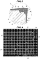
FIG. 3 schematically shows details of an A portion inFIG. 2 . -
FIG. 4 is an image of a cross section of a prototype. -
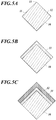
FIG. 5A is a step diagram for explaining an example of a method for manufacturing the wiring substrate according to the embodiment of the present disclosure. -
FIG. 5B is a step diagram followingFIG. 5A . -
FIG. 5C is a step diagram followingFIG. 5B . -
FIG. 6A is a step diagram followingFIG. 5C . -
FIG. 6B is a step diagram followingFIG. 6A . -
FIG. 6C is a step diagram followingFIG. 6B . -
FIG. 7A is a step diagram followingFIG. 6C . -
FIG. 7B is a step diagram followingFIG. 7A . -
FIG. 7C is a step diagram followingFIG. 7B . -
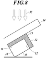
FIG. 8 is a schematic view for explaining an inclined exposure method. - Hereinafter, an embodiment of the present disclosure will be described with reference to the drawings.
-
FIG. 1 shows awiring substrate 1 according to an embodiment of the present disclosure. As shown inFIG. 1 , thewiring substrate 1 is configured such thatwiring 20 made of a conductive material is located on aninsulating substrate 10. Amain surface 11 and a side-end surface 12 of theinsulating substrate 10 are two surfaces adjacent to one another. Theinsulating substrate 10 has acorner 13 constituted by themain surface 11 and the side-end surface 12, which are two surfaces adjacent to one another. - The
wiring 20 includeswiring 21 on themain surface 11 and wiring 22 on the side-end surface 12, and is continuous across thecorner 13. Thewiring substrate 1 is for an electronic element to be mounted. On themain surface 11, a pattern having a predetermined shape for element connection is formed by thewiring 21, so that an element mounting portion is provided.FIG. 1 shows the pattern that is simplified. Thewiring 22 on the side-end surface 12 is utilized as a wiring connecting portion, such as a wire bonding region. - As shown in
FIG. 2 andFIG. 3 , t11 represents the thickness of a part of thewiring 21 disposed at an edge located at thecorner 13, and t12 represents the thickness of a part of thewiring 21 disposed away from the edge toward the inside of themain surface 11. Similarly, as shown inFIG. 2 andFIG. 3 , t21 represents the thickness of a part of thewiring 22 disposed at the edge located at thecorner 13, and t22 represents the thickness of a part of thewiring 22 disposed away from the edge toward the inside of the side-end surface 12. - An expression of t11 > t12 holds, and hence the thickness t11 is larger than the thickness t12.
- The thickness of the
wiring 21 has a gradual increase from the part of thewiring 21 disposed away from the edge toward the part of thewiring 21 disposed at the edge. - The thickness t11 of the part at the edge located at the
corner 13 being larger than the thickness t12 of the more inward part makes the connection cross-sectional area of a part of thewiring 20 across thecorner 13 large, and hence improves connection reliability of the part. - Although the thickness t11 and the thickness t12 are different from one another, the gradual increase of the thickness of the
wiring 21 toward thecorner 13 does not generate a sudden change portion of the wiring cross-sectional area, and hence can improve the connection reliability. - The effect of improving the connection reliability of the
wiring 20 at thecorner 13 can be obtained even if the wiring thickness is changed as described above on themain surface 11 only. This effect can be obtained even if the wiring thickness is changed as described above on the side-end surface 12. This is because in either case, the connection cross-sectional area of the part of thewiring 20 across thecorner 13 becomes large. In this embodiment, in order to further enhance the effect, on each of the twosurfaces end surface 12, the wiring thickness is changed in the above-described manner. - That is, an expression of t21 > t22 holds, and hence the thickness t21 is larger than the thickness t22.
- The thickness of the
wiring 22 has a gradual increase from the part of thewiring 22 disposed away from the edge toward the part of thewiring 22 disposed at the edge. - A relationship between the
wiring 21 on themain surface 11 and thewiring 22 on the side-end surface 12 is as follows. - The
wiring 21 on themain surface 11 is formed larger than thewiring 22 on the side-end surface 12. This applies to the whole, and hence the thickness of thewiring 21 is larger than the thickness of thewiring 22 without exception if parts having the same distance from thecorner 13 are compared. - Further, as to the gradient of the gradual increase of the thickness of each of the
wiring 21 and thewiring 22 toward thecorner 13, thewiring 21 on themain surface 11 has a gentler gradient than thewiring 22 on the side-end surface 12. - This ensures the thickness of the
wiring 21 on themain surface 11 that is made to have a wider area than the side-end surface 12, and hence can improve the connection reliability of thewiring 20. - Further, the thickness of the
wiring 21 on which an electronic element is to be mounted being large prevents metallic diffusion at the time of bonding of the electronic element. - Further, the gradient of the
wiring 21 on which an electronic element is to be mounted being gentle produces an effect of making the electronic element mounting portion level. - As shown in
FIG. 3 , the insulatingsubstrate 10 has a concave chippedportion 14 located at thecorner 13. As shown inFIG. 3 , thewiring 20 is located at the chippedportion 14 too. The anchoring effect due to thewiring 20 located at the chippedportion 14 raises the degree of adhesion and the bonding strength of thewiring 20 to the insulatingsubstrate 10 at thecorner 13, and hence can prevent thewiring 20 from separating from the insulatingsubstrate 10. This results in improving the connection reliability of the part of thewiring 20 across thecorner 13. -
FIG. 4 shows an image of a cross section of a prototype. - As shown in
FIG. 4 , the side-end surface 12 has surface roughness rougher than themain surface 11 to raise the bonding strength of thewiring 22, which is thinner than thewiring 21 on themain surface 11, to the side-end surface 12. On the other hand, themain surface 11 is located on a smooth surface having surface roughness finer than the side-end surface 12 and having high precision to raise element mounting performance. - Next, a manufacturing method for obtaining the
wiring substrate 1 having the above-described structure will be described. - First, a matrix substrate containing a plurality of insulating
substrates 10 used forwiring substrates 1 is processed. The main surface of the matrix substrate corresponding to surfaces that serve as themain surfaces 11 of the insulatingsubstrates 10 is polished, and then the matrix substrate is diced, and one insulatingsubstrate 10 as shown inFIG. 5A is obtained. Themain surface 11 of the insulatingsubstrate 10 is the polished surface of the matrix substrate, and the side-end surface 12 of the insulatingsubstrate 10 is the surface that has appeared by the matrix substrate being diced. Thus, themain surface 11 having high surface precision as described above and the side-end surface 12 being rough are obtained. In addition, due to chipping at the time of the dicing, the above-described chippedportion 14 is obtained. - Next, as shown in
FIG. 5B , a Cuthin film 31 is formed on themain surface 11 and the side-end surface 12 of the insulatingsubstrate 10 as a foundation layer. - Next, as shown in
FIG. 5C , a resistfilm 32 is formed on the Cuthin film 31. - Next, the resist
film 32 is exposed and developed to form a resistmask 33 as shown inFIG. 6A . For the exposure, an inclined exposure method as shown inFIG. 8 is used. As shown inFIG. 8 , aphotomask 34, themain surface 11 and the side-end surface 12 are each disposed at an angle inclined with respect to parallel light 35 for exposure. As to the angle, as shown inFIG. 8 , if an angle of themain surface 11 with respect to a plane perpendicular to theparallel light 35 for exposure is θ, it is appropriate that θ is 20 to 30 degrees. Thus, as compared with the side-end surface 12, themain surface 11 is disposed so as to be hit by theparallel light 35 for exposure more vertically. Thephotomask 34 is made to face themain surface 11. Consequently, the side-end surface 12 is disposed substantially at right angles to thephotomask 34. Hence, the further a point on the side-end surface 12 is from thecorner 13, the further the point is from thephotomask 34. There is no such a relationship on themain surface 11. - Application of this exposure method results in producing the
wiring 20 being relatively large on themain surface 11 and having a thickness that gradually increases, on each of themain surface 11 and the side-end surface 12, toward thecorner 13. Because the further a point on the side-end surface 12 is from thecorner 13, the further the point is from thephotomask 34, thewiring 22 on the side-end surface 12 is formed, as shown inFIG. 1 , so as to be wider as it is far from thecorner 13. - Next, as shown in
FIG. 6B , Cu plating is performed by using the resistmask 33 as a mask to form aCu layer 36 on the Cuthin film 31 exposed from the resistmask 33. - Next, as shown in
FIG. 6C , the resistmask 33 is removed. - Next, as shown in
FIG. 7A , etching is performed to expose the insulatingsubstrate 10 except a portion corresponding to theCu layer 36. - Next, as shown in
FIG. 7B , aprecious metal film 37 that serves as a wiring material is formed by using theCu layer 36 as a mold. - Next, as shown in
FIG. 7C , theCu layer 36 is removed to expose the insulatingsubstrate 10, so that a desired wiring pattern (37) including thewiring 20 across thecorner 13 is obtained. Thewiring 20 and the wiring pattern (37) are each, for example, a multilayer film in which, from the insulatingsubstrate 10 side, a Ti film and a Pt film, a Ti film, a Pt film and an Au film, a Ti film and a Pd film, or a Ti film, a Pd film and an Au film are disposed, for example. - As described above, according to the
wiring substrate 1 of this embodiment, the connection reliability of, of thewiring 20 continuous across thecorner 13 of the substrate, the part across thecorner 13 can be improved. - The above-described manufacturing method is merely an example of the method for obtaining the wiring substrate of the present disclosure. Needless to say, any manufacturing method is used to obtain the wiring substrate of the present disclosure.
- The present disclosure is applicable to a wiring substrate.
Claims (8)
- A wiring substrate for mounting an electronic element, comprising:
wiring is located so as to be continuous across a corner constituted by two surfaces adjacent to one another of an insulating substrate, wherein on at least one of the two surfaces, a part of the wiring disposed at an edge located at the corner has a thickness larger than a part of the wiring disposed away from the edge. - The wiring substrate according to claim 1,
wherein the thickness of the wiring has a gradual increase from the part of the wiring disposed away from the edge toward the part of the wiring disposed at the edge. - The wiring substrate according to claim 1,
wherein on each of the two surfaces, the part of the wiring disposed at the edge located at the corner has the thickness larger than the part of the wiring disposed away from the edge. - The wiring substrate according to any one of claims 1 to 3,
wherein one of the two surfaces is a main surface having an element mounting portion, and another of the two surfaces is a side-end surface. - The wiring substrate according to claim 4,
wherein the thickness of the wiring on the main surface has a gradual increase from the part of the wiring disposed away from the edge toward the part of the wiring disposed at the edge, and
wherein the thickness of the wiring on the side-end surface has a gradual increase from the part of the wiring disposed away from the edge toward the part of the wiring disposed at the edge. - The wiring substrate according to claim 5,
wherein a gradient of the gradual increase is gentler on the main surface than on the side-end surface. - The wiring substrate according to any one of claims 4 to 6,
wherein the wiring on the main surface has the thickness larger than the wiring on the side-end surface. - The wiring substrate according to any one of claims 1 to 7,
wherein the insulating substrate has a concave chipped portion located at the corner, and the wiring is located at the chipped portion.
Applications Claiming Priority (2)
| Application Number | Priority Date | Filing Date | Title |
|---|---|---|---|
| JP2018124602 | 2018-06-29 | ||
| PCT/JP2019/025764 WO2020004605A1 (en) | 2018-06-29 | 2019-06-28 | Wiring board |
Publications (2)
| Publication Number | Publication Date |
|---|---|
| EP3817520A1 true EP3817520A1 (en) | 2021-05-05 |
| EP3817520A4 EP3817520A4 (en) | 2022-04-06 |
Family
ID=68986664
Family Applications (1)
| Application Number | Title | Priority Date | Filing Date |
|---|---|---|---|
| EP19827284.1A Withdrawn EP3817520A4 (en) | 2018-06-29 | 2019-06-28 | PCB |
Country Status (5)
| Country | Link |
|---|---|
| US (1) | US11589457B2 (en) |
| EP (1) | EP3817520A4 (en) |
| JP (1) | JP7124078B2 (en) |
| CN (1) | CN112314062B (en) |
| WO (1) | WO2020004605A1 (en) |
Family Cites Families (17)
| Publication number | Priority date | Publication date | Assignee | Title |
|---|---|---|---|---|
| JPH06268368A (en) * | 1992-11-18 | 1994-09-22 | Shin Kobe Electric Mach Co Ltd | Manufacture of printed wiring board |
| JP2001102722A (en) | 1999-09-30 | 2001-04-13 | Kyocera Corp | Wiring board and method of manufacturing the same |
| JP3769514B2 (en) | 2002-03-20 | 2006-04-26 | 京セラ株式会社 | Wiring board |
| JP3891912B2 (en) * | 2002-10-09 | 2007-03-14 | 日本発条株式会社 | Disk drive suspension |
| JP2005217134A (en) * | 2004-01-29 | 2005-08-11 | Kyocera Corp | Composite wiring board and composite wiring board device |
| JP5151080B2 (en) * | 2005-07-20 | 2013-02-27 | 三菱マテリアル株式会社 | Insulating substrate, method for manufacturing insulating substrate, power module substrate and power module |
| JP2007329327A (en) * | 2006-06-08 | 2007-12-20 | Elpida Memory Inc | Semiconductor device and its manufacturing method |
| ZA200900699B (en) * | 2006-06-30 | 2010-06-30 | Sharp Kk | Power supply board, board connector, luminaire, display, and television receiver |
| JP2008275815A (en) * | 2007-04-27 | 2008-11-13 | Epson Imaging Devices Corp | Electro-optical device and electronic apparatus |
| JP5178476B2 (en) * | 2008-07-29 | 2013-04-10 | 京セラ株式会社 | Wiring board, semiconductor element storage package, and semiconductor device |
| JP5447928B2 (en) * | 2009-06-17 | 2014-03-19 | 株式会社エレメント電子 | Mounting substrate and method of manufacturing thin light emitting device using the same |
| CN104412381B (en) * | 2013-01-31 | 2018-01-09 | 京瓷株式会社 | Electronic component board for mounting electronic, electronic installation and photographing module |
| JP2015126112A (en) * | 2013-12-26 | 2015-07-06 | 日東電工株式会社 | Wiring circuit board, manufacturing method of wiring circuit board, and inspection method of wiring circuit board |
| JP6267068B2 (en) * | 2014-06-26 | 2018-01-24 | 京セラ株式会社 | Wiring board, electronic device and electronic module |
| JP6411249B2 (en) * | 2015-03-11 | 2018-10-24 | 新光電気工業株式会社 | Semiconductor device |
| JP6616209B2 (en) * | 2016-02-26 | 2019-12-04 | 株式会社平和 | Game machine |
| JP2019028304A (en) | 2017-07-31 | 2019-02-21 | 京セラ株式会社 | Wiring board and light emitting device |
-
2019
- 2019-06-28 EP EP19827284.1A patent/EP3817520A4/en not_active Withdrawn
- 2019-06-28 CN CN201980041992.3A patent/CN112314062B/en active Active
- 2019-06-28 JP JP2020527672A patent/JP7124078B2/en active Active
- 2019-06-28 US US17/256,036 patent/US11589457B2/en active Active
- 2019-06-28 WO PCT/JP2019/025764 patent/WO2020004605A1/en not_active Ceased
Also Published As
| Publication number | Publication date |
|---|---|
| WO2020004605A1 (en) | 2020-01-02 |
| CN112314062B (en) | 2023-10-10 |
| EP3817520A4 (en) | 2022-04-06 |
| JPWO2020004605A1 (en) | 2021-07-08 |
| US11589457B2 (en) | 2023-02-21 |
| US20210127486A1 (en) | 2021-04-29 |
| JP7124078B2 (en) | 2022-08-23 |
| CN112314062A (en) | 2021-02-02 |
Similar Documents
| Publication | Publication Date | Title |
|---|---|---|
| US9205443B2 (en) | Metal mask manufacturing method and metal mask | |
| US11222791B2 (en) | Printed wiring board and method for manufacturing printed wiring board | |
| TWI738712B (en) | Through electrode substrate and manufacturing method thereof | |
| JP5754209B2 (en) | Manufacturing method of semiconductor device | |
| JPH1116759A (en) | Electronic component manufacturing method | |
| EP3817520A1 (en) | Wiring board | |
| JP2022186738A (en) | Imaging device mounting board | |
| US5083234A (en) | Multilayer transducer with bonded contacts and method for implementation of bonding | |
| US11395405B2 (en) | Wiring substrate and electronic device | |
| KR101159514B1 (en) | A Structure and Manufacturing Method of Metal Wiring on Multilayered Board | |
| JP2019160911A (en) | Semiconductor device and manufacturing method of the same | |
| JP6897163B2 (en) | Through Silicon Via Substrate and Its Manufacturing Method | |
| US12021039B2 (en) | Wiring substrate | |
| JPH05206178A (en) | Semiconductor chip | |
| JP7415181B2 (en) | Mold manufacturing method | |
| JP7125679B2 (en) | Capacitor and manufacturing method thereof | |
| US8915489B2 (en) | Method for producing a flexible circuit configuration | |
| JP7405591B2 (en) | Manufacturing method of printed wiring board | |
| JP2019009151A (en) | Package substrate and manufacturing method thereof | |
| JP2024005589A (en) | Wiring board and wiring board manufacturing method | |
| JPS6243159A (en) | semiconductor equipment | |
| DE102025143144A1 (en) | Semiconductor assemblies with plasma-etched waves | |
| JP2007135129A (en) | Method for manufacturing piezoelectric vibrating piece and piezoelectric vibrating piece manufactured by the manufacturing method | |
| JP2023073430A (en) | Substrates for semiconductor devices and semiconductor devices | |
| JPS60130145A (en) | Beam lead type semiconductor device |
Legal Events
| Date | Code | Title | Description |
|---|---|---|---|
| STAA | Information on the status of an ep patent application or granted ep patent |
Free format text: STATUS: THE INTERNATIONAL PUBLICATION HAS BEEN MADE |
|
| PUAI | Public reference made under article 153(3) epc to a published international application that has entered the european phase |
Free format text: ORIGINAL CODE: 0009012 |
|
| STAA | Information on the status of an ep patent application or granted ep patent |
Free format text: STATUS: REQUEST FOR EXAMINATION WAS MADE |
|
| 17P | Request for examination filed |
Effective date: 20201228 |
|
| AK | Designated contracting states |
Kind code of ref document: A1 Designated state(s): AL AT BE BG CH CY CZ DE DK EE ES FI FR GB GR HR HU IE IS IT LI LT LU LV MC MK MT NL NO PL PT RO RS SE SI SK SM TR |
|
| DAV | Request for validation of the european patent (deleted) | ||
| DAX | Request for extension of the european patent (deleted) | ||
| REG | Reference to a national code |
Ref country code: DE Ref legal event code: R079 Free format text: PREVIOUS MAIN CLASS: H05K0001020000 Ipc: H05K0003100000 |
|
| A4 | Supplementary search report drawn up and despatched |
Effective date: 20220303 |
|
| RIC1 | Information provided on ipc code assigned before grant |
Ipc: H05K 3/40 20060101ALI20220225BHEP Ipc: H05K 3/10 20060101AFI20220225BHEP |
|
| P01 | Opt-out of the competence of the unified patent court (upc) registered |
Effective date: 20230508 |
|
| STAA | Information on the status of an ep patent application or granted ep patent |
Free format text: STATUS: EXAMINATION IS IN PROGRESS |
|
| 17Q | First examination report despatched |
Effective date: 20241127 |
|
| STAA | Information on the status of an ep patent application or granted ep patent |
Free format text: STATUS: THE APPLICATION HAS BEEN WITHDRAWN |
|
| 18W | Application withdrawn |
Effective date: 20250331 |