EP3812908B1 - Verfahren und vorrichtung zum testen eines chips zur verwendung in künstlicher intelligenz, vorrichtung und speichermedium - Google Patents
Verfahren und vorrichtung zum testen eines chips zur verwendung in künstlicher intelligenz, vorrichtung und speichermedium Download PDFInfo
- Publication number
- EP3812908B1 EP3812908B1 EP20204930.0A EP20204930A EP3812908B1 EP 3812908 B1 EP3812908 B1 EP 3812908B1 EP 20204930 A EP20204930 A EP 20204930A EP 3812908 B1 EP3812908 B1 EP 3812908B1
- Authority
- EP
- European Patent Office
- Prior art keywords
- test
- arithmetic unit
- dft
- arithmetic
- logic circuit
- Prior art date
- Legal status (The legal status is an assumption and is not a legal conclusion. Google has not performed a legal analysis and makes no representation as to the accuracy of the status listed.)
- Active
Links
Images




Classifications
-
- G—PHYSICS
- G01—MEASURING; TESTING
- G01R—MEASURING ELECTRIC VARIABLES; MEASURING MAGNETIC VARIABLES
- G01R31/00—Arrangements for testing electric properties; Arrangements for locating electric faults; Arrangements for electrical testing characterised by what is being tested not provided for elsewhere
- G01R31/28—Testing of electronic circuits, e.g. by signal tracer
- G01R31/317—Testing of digital circuits
- G01R31/3177—Testing of logic operation, e.g. by logic analysers
-
- G—PHYSICS
- G06—COMPUTING OR CALCULATING; COUNTING
- G06F—ELECTRIC DIGITAL DATA PROCESSING
- G06F11/00—Error detection; Error correction; Monitoring
- G06F11/22—Detection or location of defective computer hardware by testing during standby operation or during idle time, e.g. start-up testing
- G06F11/2205—Detection or location of defective computer hardware by testing during standby operation or during idle time, e.g. start-up testing using arrangements specific to the hardware being tested
- G06F11/2236—Detection or location of defective computer hardware by testing during standby operation or during idle time, e.g. start-up testing using arrangements specific to the hardware being tested to test CPU or processors
-
- G—PHYSICS
- G06—COMPUTING OR CALCULATING; COUNTING
- G06F—ELECTRIC DIGITAL DATA PROCESSING
- G06F11/00—Error detection; Error correction; Monitoring
- G06F11/22—Detection or location of defective computer hardware by testing during standby operation or during idle time, e.g. start-up testing
- G06F11/2205—Detection or location of defective computer hardware by testing during standby operation or during idle time, e.g. start-up testing using arrangements specific to the hardware being tested
- G06F11/2226—Detection or location of defective computer hardware by testing during standby operation or during idle time, e.g. start-up testing using arrangements specific to the hardware being tested to test ALU
-
- G—PHYSICS
- G06—COMPUTING OR CALCULATING; COUNTING
- G06F—ELECTRIC DIGITAL DATA PROCESSING
- G06F30/00—Computer-aided design [CAD]
- G06F30/30—Circuit design
- G06F30/32—Circuit design at the digital level
- G06F30/333—Design for testability [DFT], e.g. scan chain or built-in self-test [BIST]
-
- G—PHYSICS
- G06—COMPUTING OR CALCULATING; COUNTING
- G06F—ELECTRIC DIGITAL DATA PROCESSING
- G06F11/00—Error detection; Error correction; Monitoring
- G06F11/22—Detection or location of defective computer hardware by testing during standby operation or during idle time, e.g. start-up testing
- G06F11/2273—Test methods
-
- G—PHYSICS
- G06—COMPUTING OR CALCULATING; COUNTING
- G06F—ELECTRIC DIGITAL DATA PROCESSING
- G06F30/00—Computer-aided design [CAD]
- G06F30/30—Circuit design
- G06F30/32—Circuit design at the digital level
- G06F30/33—Design verification, e.g. functional simulation or model checking
-
- G—PHYSICS
- G06—COMPUTING OR CALCULATING; COUNTING
- G06F—ELECTRIC DIGITAL DATA PROCESSING
- G06F30/00—Computer-aided design [CAD]
- G06F30/30—Circuit design
- G06F30/32—Circuit design at the digital level
- G06F30/337—Design optimisation
-
- G—PHYSICS
- G06—COMPUTING OR CALCULATING; COUNTING
- G06N—COMPUTING ARRANGEMENTS BASED ON SPECIFIC COMPUTATIONAL MODELS
- G06N5/00—Computing arrangements using knowledge-based models
- G06N5/02—Knowledge representation; Symbolic representation
-
- G—PHYSICS
- G01—MEASURING; TESTING
- G01R—MEASURING ELECTRIC VARIABLES; MEASURING MAGNETIC VARIABLES
- G01R31/00—Arrangements for testing electric properties; Arrangements for locating electric faults; Arrangements for electrical testing characterised by what is being tested not provided for elsewhere
- G01R31/28—Testing of electronic circuits, e.g. by signal tracer
- G01R31/317—Testing of digital circuits
- G01R31/31701—Arrangements for setting the Unit Under Test [UUT] in a test mode
-
- G—PHYSICS
- G01—MEASURING; TESTING
- G01R—MEASURING ELECTRIC VARIABLES; MEASURING MAGNETIC VARIABLES
- G01R31/00—Arrangements for testing electric properties; Arrangements for locating electric faults; Arrangements for electrical testing characterised by what is being tested not provided for elsewhere
- G01R31/28—Testing of electronic circuits, e.g. by signal tracer
- G01R31/317—Testing of digital circuits
- G01R31/31703—Comparison aspects, e.g. signature analysis, comparators
-
- G—PHYSICS
- G01—MEASURING; TESTING
- G01R—MEASURING ELECTRIC VARIABLES; MEASURING MAGNETIC VARIABLES
- G01R31/00—Arrangements for testing electric properties; Arrangements for locating electric faults; Arrangements for electrical testing characterised by what is being tested not provided for elsewhere
- G01R31/28—Testing of electronic circuits, e.g. by signal tracer
- G01R31/317—Testing of digital circuits
- G01R31/31704—Design for test; Design verification
-
- G—PHYSICS
- G01—MEASURING; TESTING
- G01R—MEASURING ELECTRIC VARIABLES; MEASURING MAGNETIC VARIABLES
- G01R31/00—Arrangements for testing electric properties; Arrangements for locating electric faults; Arrangements for electrical testing characterised by what is being tested not provided for elsewhere
- G01R31/28—Testing of electronic circuits, e.g. by signal tracer
- G01R31/317—Testing of digital circuits
- G01R31/3181—Functional testing
- G01R31/3185—Reconfiguring for testing, e.g. LSSD, partitioning
- G01R31/318516—Test of programmable logic devices [PLDs]
- G01R31/318519—Test of field programmable gate arrays [FPGA]
-
- G—PHYSICS
- G01—MEASURING; TESTING
- G01R—MEASURING ELECTRIC VARIABLES; MEASURING MAGNETIC VARIABLES
- G01R31/00—Arrangements for testing electric properties; Arrangements for locating electric faults; Arrangements for electrical testing characterised by what is being tested not provided for elsewhere
- G01R31/28—Testing of electronic circuits, e.g. by signal tracer
- G01R31/317—Testing of digital circuits
- G01R31/3181—Functional testing
- G01R31/3185—Reconfiguring for testing, e.g. LSSD, partitioning
- G01R31/318533—Reconfiguring for testing, e.g. LSSD, partitioning using scanning techniques, e.g. LSSD, Boundary Scan, JTAG
- G01R31/318583—Design for test
-
- G—PHYSICS
- G01—MEASURING; TESTING
- G01R—MEASURING ELECTRIC VARIABLES; MEASURING MAGNETIC VARIABLES
- G01R31/00—Arrangements for testing electric properties; Arrangements for locating electric faults; Arrangements for electrical testing characterised by what is being tested not provided for elsewhere
- G01R31/28—Testing of electronic circuits, e.g. by signal tracer
- G01R31/317—Testing of digital circuits
- G01R31/3181—Functional testing
- G01R31/319—Tester hardware, i.e. output processing circuits
- G01R31/31903—Tester hardware, i.e. output processing circuits tester configuration
- G01R31/31912—Tester/user interface
-
- G—PHYSICS
- G01—MEASURING; TESTING
- G01R—MEASURING ELECTRIC VARIABLES; MEASURING MAGNETIC VARIABLES
- G01R31/00—Arrangements for testing electric properties; Arrangements for locating electric faults; Arrangements for electrical testing characterised by what is being tested not provided for elsewhere
- G01R31/28—Testing of electronic circuits, e.g. by signal tracer
- G01R31/317—Testing of digital circuits
- G01R31/3181—Functional testing
- G01R31/319—Tester hardware, i.e. output processing circuits
- G01R31/3193—Tester hardware, i.e. output processing circuits with comparison between actual response and known fault free response
-
- G—PHYSICS
- G01—MEASURING; TESTING
- G01R—MEASURING ELECTRIC VARIABLES; MEASURING MAGNETIC VARIABLES
- G01R31/00—Arrangements for testing electric properties; Arrangements for locating electric faults; Arrangements for electrical testing characterised by what is being tested not provided for elsewhere
- G01R31/28—Testing of electronic circuits, e.g. by signal tracer
- G01R31/317—Testing of digital circuits
- G01R31/3181—Functional testing
- G01R31/319—Tester hardware, i.e. output processing circuits
- G01R31/3193—Tester hardware, i.e. output processing circuits with comparison between actual response and known fault free response
- G01R31/31932—Comparators
-
- G—PHYSICS
- G06—COMPUTING OR CALCULATING; COUNTING
- G06F—ELECTRIC DIGITAL DATA PROCESSING
- G06F2115/00—Details relating to the type of the circuit
- G06F2115/08—Intellectual property [IP] blocks or IP cores
Definitions
- This application relates to the field of data processing technologies, and especially, to the artificial intelligence technology.
- AI chips artificial intelligence chips
- DFT Design for Test
- a DFT test is still performed on AI chips in a traditional chip test manner. Because traditional chips often have large heterogeneous IP cores, the DFT tests of the traditional chips are often completed on a chip level or on a large heterogeneous IP core, which also increases the test time of the traditional chips.
- AI chips have a different structure from the traditional chips. An AI chip has numerous same AI arithmetic units to process AI algorithms, the numerous same AI arithmetic units are the core of the entire AI chip, and the AI chip has a huge size.
- the traditional chips test manner in the prior art is no longer applicable to the AI chips.
- Using the traditional chip test manner to test the AI chips will increase the test time, cost and test power consumption of the AI chips, and reduce the test efficiency of the AI chips.
- US 2007/136732 A1 relates to efficiently testing a plurality of ALUs by equipping each ALU with its own dedicated test vector generation circuitry, and a subset is chosen from those ALUs which are used in actual operation.
- US 2011/275170 A1 describes a tool to aid a test engineer in creating a concurrent test plan and teaches to divide a plurality of dies on a wafer into subsets and to concurrently test these subsets, the criterion to construct the subsets being unrelated to the waiter size respectively the number of dies on the wafer.
- the criterion resorted to is the hardware configuration (pins) of the dies.
- US 5822557A describes an arithmetic operation unit for operating according to pipeline control and an instruction decoder for controlling the arithmetic operation unit by decoding an instruction, and teaches that arithmetic units 1010-0 ... 100-n-1 are operated individually in test mode.
- Embodiments of this application provides a method and apparatus for testing an artificial intelligence chip, a device and a storage medium, to solve the technical problem that the traditional chip test manner in the prior art is no longer applicable to the AI chips and that using the traditional chip test manner to test the AI chips increases the test time, cost and test power consumption of the AI chips, and reduces the test efficiency of the AI chips.
- a first aspect of the embodiments of the present application provides a method for testing an artificial intelligence chip, wherein a target artificial intelligence chip has multiple same arithmetic units, the method includes: obtaining scale information of the target artificial intelligence chip; determining whether the target artificial intelligence chip satisfies a test condition of an arithmetic unit array level according to the scale information; dividing all the arithmetic units into multiple same arithmetic unit arrays, and performing a Designed for Test (DFT) test on the arithmetic unit arrays, respectively, if it is determined that the test condition of the arithmetic unit array level is satisfied; performing the DFT test on the arithmetic units, respectively, if it is determined the test condition of the arithmetic unit array level is not satisfied.
- DFT Designed for Test
- the test logic circuit and the test vector of each arithmetic unit array or arithmetic unit are completely the same, so the test cost is reduced.
- the number of transistors in each arithmetic unit or arithmetic unit array is very small, so the size of test vectors is also small, and thus the test time is greatly reduced and the test efficiency is improved.
- loading the DFT of each arithmetic unit or arithmetic unit array will require far less computing and storing resources of the memory, which greatly reduces the test power consumption.
- the scale information includes a number of transistors of an arithmetic unit
- the determining whether the target artificial intelligence chip satisfies a test condition for an arithmetic unit array level according to the scale information includes: determining whether the number of the transistors is smaller than a preset scale threshold; determining that the test condition of the arithmetic unit array level is satisfied, if it is determined that the number of the transistors is less than the preset scale threshold; determining that the test condition of the arithmetic unit array level is not satisfied, if it is determined that the number of the transistors is greater than or equal to the preset scale threshold.
- the number of the transistors is smaller than the preset scale threshold. If it is determined that the number of the transistors is smaller than the preset scale threshold, it means that the size of each arithmetic unit is particularly small. Then, it is determined that the test condition of the arithmetic unit array level is satisfied, and multiple arithmetic units can be assembled to form an arithmetic unit array to perform the test on the arithmetic unit array level. If it is determined that the number of the transistors is greater than or equal to the preset scale threshold, it means that the size of each arithmetic unit is relatively large.
- the size of the arithmetic unit array or the arithmetic unit can meet the requirement of an individual test, which can further reduce the test time.
- the dividing all the arithmetic units into multiple same arithmetic unit arrays includes: determining a number of arithmetic units in an arithmetic unit array according to the number of the transistors and the total number of the arithmetic units; dividing all the arithmetic units into the multiple same arithmetic unit arrays according to the number of the arithmetic units.
- all the arithmetic units are divided into multiple same arithmetic unit arrays according to the number of the transistors and the total number of the arithmetic units, so that the arithmetic units in the artificial intelligence chip can be evenly divided into the same arithmetic unit arrays, and the size of each arithmetic unit array is not too large, which can meet the requirement of the individual test, and thus can reduce the test time.
- each of the arithmetic unit arrays is provided with a first test logic circuit; the performing a DFT test on the arithmetic unit arrays, respectively, includes: generating first test vectors corresponding to the arithmetic unit arrays, where the first test vectors corresponding to respective one of the arithmetic unit arrays are the same; performing the DFT test on the arithmetic unit arrays, respectively, by inputting the first test vectors into first test logic circuits corresponding to respective ones of the arithmetic unit arrays, respectively; outputting test results corresponding to respective ones of the arithmetic unit arrays.
- a first test logic circuit is provided in each arithmetic unit array, and the same first test vector is used to test each arithmetic unit array, respectively, and the test results are output. Since the first test logic circuit and the first test vector of each arithmetic unit array are the same, the test cost is greatly reduced.
- the first test logic circuit includes: a first test interface; the performing the DFT test on the arithmetic unit arrays, respectively, by inputting the first test vectors into first test logic circuit corresponding to respective ones of the arithmetic unit arrays, respectively, includes: performing the DFT test on the arithmetic unit arrays in parallel, by broadcasting, through respective first test interfaces, the first test vectors to the first test logic circuits of corresponding arithmetic unit arrays.
- the first test logic circuit includes a first test interface
- the electronic device broadcasts the first test vectors to the first test logic circuits of the corresponding arithmetic unit arrays through respective first test interfaces, so that the DFT test can be performed on each arithmetic unit array simultaneously.
- the test time of the AI chip is reduced to the test time of a single arithmetic unit array, which further greatly reduces the test time.
- each of the arithmetic units is provided with a second test logic circuit; the performing the DFT test on the arithmetic units, respectively, includes: generating second test vectors corresponding to the arithmetic units, where the second test vectors corresponding to respective ones of the arithmetic units are the same; performing the DFT test on the arithmetic units, respectively, by inputting the second test vectors into second test logic circuits corresponding to respective ones of the arithmetic units, respectively; outputting test results corresponding to respective ones of the arithmetic units.
- a second test logic circuit is provided in each arithmetic unit, and the same second test vector is used to test each arithmetic unit, respectively, and the test results are output. Since the second test logic circuit and the second test vector of each arithmetic unit are same, the test cost is greatly reduced.
- the second test logic circuit includes: a second test interface; the performing the DFT test on the arithmetic units, respectively, by inputting the second test vectors into second test logic circuits corresponding to respective ones of the arithmetic units, respectively, includes: performing the DFT test on the arithmetic units in parallel, by broadcasting, through respective second test interfaces, the second test vectors to the second test logic circuits of corresponding arithmetic units.
- the second test logic circuit includes a second test interface, and the electronic device broadcasts the second test vectors to the second test logic circuits of the corresponding arithmetic units through respective second test interfaces, so that the DFT test can be performed on each arithmetic unit simultaneously.
- the test time of the AI chip is reduced to the test time of a single arithmetic unit, which further greatly reduces the test time.
- the method further includes: performing a test on at least one first preset DFT logic circuit in the first test logic circuit at a register-transfer level (RTL) stage of the target artificial intelligence chip; and if the first preset DFT logic circuit fails the test, then repairing the first preset DFT logic circuit at the RTL stage of the target artificial intelligence chip,
- some first preset DFT logic circuits of the first test logic circuit in the DFT of the arithmetic unit array can be designed and tested at the RTL stage of the target artificial intelligence chip, so that a corresponding test can be accomplished earlier, and there is no need to wait for the entire AI chip to complete before starting the design and test. And if the first preset DFT logic circuit fails the test, the first preset DFT logic circuit is modified, and when the modified first preset DFT logic circuit is tested again, the iteration process does not need to be continuously performed between the DFT configuration and the test vectors generation, but instead, the test can be continued before the test vectors are executed, so as to avoid the waste of test time caused by such continuous iteration. The test and repair time of the first preset DFT logic circuit can be effectively reduced.
- the method before the performing the DFT test on the arithmetic units, respectively, the method further includes: performing a test on at least one second preset DFT logic circuit in the second test logic circuit at the RTL stage of the target artificial intelligence chip; repairing the second preset DFT logic circuit at the RTL stage of the target artificial intelligence chip, if the second preset DFT logic circuit fails the test.
- some second preset DFT logic circuits of the second test logic circuit in the DFT of the arithmetic unit can be designed and tested at the RTL stage of the target artificial intelligence chip. So that a corresponding test can be completed earlier, and there is no need to wait for the entire AI chip to complete before starting the design and test. And if the second preset DFT logic circuit fails the test, the second preset DFT logic circuit is modified, and when the modified second preset DFT logic circuit is tested again, the iteration process does not need to be continuously performed between the DFT configuration and the generation of test vectors, but instead, the test can be continued before the test vectors are executed, so as to avoid the waste of test time caused by this continuous iteration. The test and repair time of the second preset DFT logic circuit can be reduced.
- a second aspect of the embodiments of the present application provides an apparatus for testing an artificial intelligence chip, wherein a target artificial intelligence chip has multiple same arithmetic units
- the apparatus includes: a scale information obtaining module, configured to obtain scale information of the target artificial intelligence chip; a test condition determining module, configured to determine whether the target artificial intelligence chip satisfies a test condition of an arithmetic unit array level according to the scale information; an array testing module, configured to divide all the arithmetic units into multiple same arithmetic unit arrays, and performing a DFT test on the arithmetic unit arrays, respectively, if it is determined that the test condition of the arithmetic unit array level is satisfied; an arithmetic unit testing module, configured to perform the DFT test on the arithmetic units, respectively, if it is determined that the test condition of the arithmetic unit array level is not satisfied.
- the scale information comprises a number of transistors in an arithmetic unit
- the test condition determining module is specifically configured to: determine whether the number of the transistors is smaller than a preset scale threshold; determine the test condition of the arithmetic unit array level is satisfied, if it is determined that the number of the transistors is less than the preset scale threshold; determine the test condition of the arithmetic unit array level is not satisfied, if it is determined that the number of the transistors is greater than or equal to the preset scale threshold.
- the array testing module when dividing all arithmetic units into multiple same arithmetic unit arrays, is specifically configured to: determine a number of arithmetic units in an arithmetic unit array according to the number of the transistors and the total number of the arithmetic units; divide all the arithmetic units into the multiple same arithmetic unit arrays according to the number of the arithmetic units.
- each of the arithmetic unit arrays is provided with a first test logic circuit; when performing DFT tests on the arithmetic unit arrays, respectively, the array testing module is specifically configured to: generate first test vectors corresponding to the arithmetic unit arrays, where the first test vectors corresponding to respective ones of the arithmetic unit arrays are the same; perform the DFT test on the arithmetic unit arrays, respectively, by inputting the first test vectors into first test logic circuits corresponding to respective ones of the arithmetic unit arrays, respectively; outputting test results corresponding to respective ones of the arithmetic unit arrays.
- the first test logic circuit comprises: a first test interface; when performing the DFT test on the arithmetic unit arrays, respectively, by inputting the first test vectors into first test logic circuits corresponding to respective ones of the arithmetic unit arrays, respectively, the array testing module is specifically configured to: perform the DFT test on the arithmetic unit arrays in parallel by broadcasting, through respective first test interfaces, the first test vectors to the first test logic circuits of corresponding arithmetic unit arrays.
- each of the arithmetic units is provided with a second test logic circuit; when performing the DFT test on the arithmetic units, respectively, the arithmetic unit testing module is specifically configured to: generate second test vectors corresponding to the arithmetic units, where the second test vectors corresponding to respective ones of the arithmetic units are the same; perform the DFT test on the arithmetic units, respectively, by inputting the second test vectors into second test logic circuits corresponding to respective ones of the arithmetic units, respectively; outputting test results corresponding to respective ones of the arithmetic units.
- the second test logic circuit includes: a second test interface; when performing the DFT test on the arithmetic units, respectively, by inputting the second test vectors into second test logic circuits corresponding to respective ones of the arithmetic units, respectively, the arithmetic unit testing module is specifically configured to: perform the DFT test on the arithmetic units in parallel by broadcasting, through respective second test interfaces, the second test vectors to the second test logic circuits of corresponding arithmetic units.
- the apparatus as described above further includes: a first circuit testing and repairing module, configured to perform a test on at least one first preset DFT logic circuit in the first test logic circuit at an RTL stage of the target artificial intelligence chip; and repair the first preset DFT logic circuit at the RTL stage of the target artificial intelligence chip if the first preset DFT logic circuit fails the test.
- a first circuit testing and repairing module configured to perform a test on at least one first preset DFT logic circuit in the first test logic circuit at an RTL stage of the target artificial intelligence chip; and repair the first preset DFT logic circuit at the RTL stage of the target artificial intelligence chip if the first preset DFT logic circuit fails the test.
- the apparatus as described above further includes: a second circuit testing and repairing module, configured to perform a test on at least one second preset DFT logic circuit in the second test logic circuit at the RTL stage of the target artificial intelligence chip; repair the second preset DFT logic circuit at the RTL stage of the target artificial intelligence chip, if the second preset DFT logic circuit fails the test.
- a second circuit testing and repairing module configured to perform a test on at least one second preset DFT logic circuit in the second test logic circuit at the RTL stage of the target artificial intelligence chip; repair the second preset DFT logic circuit at the RTL stage of the target artificial intelligence chip, if the second preset DFT logic circuit fails the test.
- a third aspect of the embodiments of the present application provides an electronic device, including: at least one processor; and a memory communicatively connected to the at least one processor; wherein, the memory stores instructions executable by the at least one processor, and the instructions when being executed by the at least one processor cause the at least one processor to execute any method according to the first aspect.
- a fourth aspect of the embodiments of the present application provides a non-transitory computer-readable storage medium having computer instructions stored thereon, and the computer instructions are used to cause the computer to perform any method according to the first aspect.
- a fifth aspect of the embodiments of the present application provides a computer program, including program code, and when a computer runs the computer program, the program code executes the method according to the first aspect.
- Artificial intelligence chip also called AI accelerator or computing card, is a module dedicated to processing a large number of computing tasks in artificial intelligence applications. CPU is still responsible for other non-computing tasks.
- AI chips are mainly divided into GPUs, FPGAs, and ASICs.
- an algorithm logic unit is the core of the entire AI chip, and usually occupies a high proportion in the entire AI chip.
- the AI algorithm logic unit is usually composed of the same arithmetic units.
- the size of an AI chip is huge, so there are a large number of same arithmetic units in the AI chip.
- a traditional chip often has multiple large heterogeneous IP cores, such as a power consumption control module, a communication interface module, a video analysis module, etc.
- Design for Test is an integrated circuit design technology. The main task is to design a specific test logic circuit by adding logic, replacing components and adding pins, etc., and meanwhile adjust the structure of the circuit under test to improve the testability, i.e. the controllability and observability, of the circuit. Adding these structures in the design stage increases the complexity of the circuit and seems to increase the cost, but it can often save more time and cost in the test stage.
- a DFT test of an AI chip is generally a chip-level test.
- a test machine has a limit on how many test units are connected in series to form a scan chain, so firstly, scan chains are inserted between the arithmetic units of the AI chip, and each scan chain is connected to a different number of arithmetic units. Then each scan chain is provided with a test logic circuit, and a test vector corresponding to each scan chain is generated, and each scan chain corresponds to a different test logic circuit and test vector.
- the test machine sends the test vector corresponding to each scan chain to the AI chip to input the test vector into the test logic circuit of the corresponding scan chain, so as to complete the test of the arithmetic units on the scan chain. Because there are many arithmetic units on each scan chain, the size of the test vector is generally very large, and the test time will be very long. Moreover, the test logic circuit on each scan chain is different with each other, and the test vector is also different, so the test cost is increased. Loading the entire DFT requires a large number of computing and storing resources of the memory, and the test power consumption is also be constrained.
- the AI chip Since the structure of the AI chip is different from the traditional chip, the AI chip has a huge size and includes a large number of the same arithmetic units. The large numbers of the same arithmetic units occupy a major proportion of the AI chip. Therefore, based on the structural characteristics of the AI chip and aiming at the technical problem of the method for testing an AI chip in the prior art, the embodiments of the present application propose a method for testing an AI chip.
- the application scenario corresponding to the method for testing an artificial intelligence chip provided in the embodiments of the present application includes: an electronic device and a target artificial intelligence chip.
- the electronic device may be a test machine.
- the electronic device can communicate with the target artificial intelligence chip.
- Scale information of the target artificial intelligence chip can be obtained. Since the target artificial intelligence chip has multiple same arithmetic units, whether the target artificial intelligence chip satisfies a test condition of an arithmetic unit array level is determined according to the scale information.
- all the arithmetic units are divided into multiple same arithmetic unit arrays, and a DFT test is performed on each arithmetic unit array, respectively. If it is determined that the test condition of the arithmetic unit array level is not satisfied, the DFT test is performed on each arithmetic unit, respectively. Then, the DFT test of the artificial intelligence chip is completed. After the DFT test is performed on each arithmetic unit array, respectively, a test result of each arithmetic unit array is determined. Or, after the DFT test is performed on each arithmetic unit, respectively, a test result of each arithmetic unit is determined.
- the arithmetic unit array or arithmetic unit that failed the test is repaired. Since the same arithmetic unit arrays or arithmetic units of the artificial intelligence chip are tested respectively, the test logic circuit and the test vector of each arithmetic unit array or arithmetic unit are completely the same, and thus the test cost is reduced. In addition, there are a small number of the transistors in each arithmetic unit or arithmetic unit array, so the size of the test vector is also small, and thus the test time is greatly reduced and the test efficiency is improved. In addition, loading the DFT of each arithmetic unit or arithmetic unit array requires far less computing and storing resources of the memory, which greatly reduces the test power consumption.
- FIG. 2 is a schematic flowchart of a method for testing an artificial intelligence chip according to the first embodiment of the present application.
- the executive entity of the embodiment of the present application is an apparatus for testing an artificial intelligence chip.
- the apparatus for testing an artificial intelligence chip may be integrated in an electronic device, and the electronic device may be a test machine.
- the method for testing an artificial intelligence chip provided in this embodiment includes the following steps.
- Step 101 obtaining scale information of a target artificial intelligence chip.
- the target artificial intelligence chip is an artificial intelligence chip that needs to be tested.
- the target artificial intelligence chip includes multiple same arithmetic units.
- the scale information of the target artificial intelligence chip can be stored in a storage device.
- the storage device may be a computer, a U disk, a magnetic disk or other devices, and the scale information of the target artificial intelligence chip can be obtained by accessing the storage device.
- the scale information may include: the total number of arithmetic units, a number of transistors in each arithmetic unit, and so on.
- the transistors in the arithmetic units are a kind of semiconductor devices, which are basic building blocks of the arithmetic units.
- Step 102 determining whether the target artificial intelligence chip satisfies a test condition of an arithmetic unit array level according to the scale information.
- whether the target artificial intelligence chip satisfies the test condition of the arithmetic unit array level can be determined according to the total number of the arithmetic units. If the total number of the arithmetic units is small, then the DFT test can be performed on each arithmetic unit respectively, then it is determined that the test condition of the arithmetic unit array level is not satisfied. If the total number of the arithmetic units is large, it is determined that the test condition of the arithmetic unit array level is satisfied. Then, the DFT test can be performed on each arithmetic unit array, respectively.
- the total number of the arithmetic units may be compared with a preset number threshold. If the total number of the arithmetic units is less than the preset number threshold, it is determined that the total number of the arithmetic units is small. If the total number of the arithmetic units is greater than or equal to the preset number threshold, it is determined that the total number of the arithmetic units is large.
- whether the target artificial intelligence chip satisfies the test condition of the arithmetic unit array level may also be determined according to the number of transistors in an arithmetic unit. If it is determined that the number of the transistors is smaller than a preset scale threshold, it means that the size of each arithmetic unit is small, and it is determined that the test condition of the arithmetic unit array level is satisfied, and the DFT test may be performed on each arithmetic unit array, respectively. If it is determined that the number of the transistors is greater than or equal to the preset scale threshold, it is determined the test condition of the arithmetic unit array level is not satisfied, and the DFT test may be performed on each arithmetic unit, respectively.
- Step 103 dividing all the arithmetic units into multiple same arithmetic unit arrays and performing a DFT test on the arithmetic unit arrays, respectively, if it is determined that the test condition of the arithmetic unit array level is satisfied.
- all the arithmetic units when all the arithmetic units are divided into multiple same arithmetic unit arrays, all the arithmetic units may be divided into multiple same arithmetic unit arrays according to the total number of the arithmetic units. That is, the number of arithmetic units included in each arithmetic unit array is the same. Or, all the arithmetic units are divided into multiple identical arithmetic unit arrays in other ways, which is not limited in this embodiment.
- each arithmetic unit array includes four arithmetic units.
- the four arithmetic units encircled in FIG. 3 form one arithmetic unit array.
- test logic circuit when the DFT test is performed on the arithmetic unit arrays, respectively, a test logic circuit needs to be provided in each arithmetic unit array, where the test logic circuit includes a scan chain, and the scan chain is inserted into the arithmetic unit array. Test vectors for the arithmetic unit arrays can also be generated to complete the DFT test for each arithmetic unit array.
- test logic circuits and scan chains provided, as well as the test vectors generated, are the same.
- the DFT test when the DFT test is performed on the arithmetic unit arrays, respectively, the DFT test may be performed on an arithmetic unit array after the DFT test on another arithmetic unit array is completed. Or, the arithmetic unit arrays may be divided into different groups, and the DFT test is performed on a group of arithmetic unit arrays in parallel after the DFT test on another group of arithmetic unit arrays is completed in parallel. Or, the DFT test may be performed on all the arithmetic unit arrays in parallel simultaneously, which is not limited in this embodiment.
- Step 104 performing the DFT test on the arithmetic units, respectively, if it is determined that the test condition of the arithmetic unit array level is not satisfied.
- test condition of the arithmetic unit array level if it is determined that the test condition of the arithmetic unit array level is not satisfied, it means that the test condition of the arithmetic unit level is satisfied, and then the DFT test is performed on the arithmetic units, respectively.
- test logic circuit When performing the DFT test on each arithmetic unit, a test logic circuit needs to be provided in each arithmetic unit, where the test logic circuit includes a scan chain, and the scan chain is inserted into the arithmetic unit. Test vectors for the arithmetic units may also be generated to complete the DFT test on each arithmetic unit.
- test logic circuits and scan chains provided to the arithmetic units, as well as the test vectors generated, are the same.
- the DFT test when the DFT test is performed on the arithmetic units, respectively, the DFT test may be performed on an arithmetic unit after the DFT test on another arithmetic unit is completed, or the DFT test may be performed on all the arithmetic units in parallel simultaneously, which is not limited in this embodiment.
- test logic circuit corresponding to the arithmetic unit array is different from the test logic circuit corresponding to the arithmetic unit.
- the test vector corresponding to the arithmetic unit array and the test vector corresponding to the arithmetic unit are also different.
- scale information of a target artificial intelligence chip is obtained; whether the target artificial intelligence chip satisfies a test condition of an arithmetic unit array level is determined according to the scale information; all the arithmetic units are divided into multiple same arithmetic unit arrays and a DFT test is performed on the arithmetic unit arrays, respectively, if it is determined the test condition of the arithmetic unit array level is satisfied; the DFT test is performed on the arithmetic units, respectively, if it is determined that the test condition of the arithmetic unit array level is not satisfied.
- the test logic circuit and the test vector of each arithmetic unit array or arithmetic unit are completely the same, so the test cost is reduced.
- the size of the test vector is also small, and thus the test time is greatly reduced and the test efficiency is improved.
- loading the DFT of each arithmetic unit or arithmetic unit array requires far less computing and storing resources of the memory, which greatly reduces the test power consumption.
- FIG. 4 is a schematic flowchart of a method for testing an artificial intelligence chip according to the second embodiment of the present application. As shown in FIG. 4 , the method for testing an artificial intelligence chip provided in this embodiment further refines steps 101-104 based on the method for testing an artificial intelligence chip provided in the first embodiment of the present application. The method for testing an artificial intelligence chip provided in this embodiment includes the following steps.
- Step 201 obtaining a number of transistors in an arithmetic unit of a target artificial intelligence chip.
- the number of the transistors in the arithmetic unit of the artificial intelligence chip is directly obtained, so as to determine, according to the number of the transistors, whether to perform the test on an arithmetic unit array level or on an arithmetic unit level.
- Step 202 determining whether the number of the transistors is smaller than a preset scale threshold, if yes, performing step 203, otherwise, performing step 205.
- the value of the preset scale threshold is not limited, which can be determined according to multiple tests.
- the test condition of the arithmetic unit array level is not satisfied, but the test condition of the arithmetic unit level is satisfied, and the test is performed on the arithmetic unit level.
- the determination on whether the test condition of the arithmetic unit array is satisfied is performed by determining whether the number of the transistors in the arithmetic unit is less than the preset scale threshold, so that the size of the arithmetic unit array or arithmetic unit can meet the requirement of an individual test, further reducing the test time.
- Step 203 dividing all the arithmetic units into multiple same arithmetic unit arrays.
- step 203 includes the following steps.
- Step 2031 determining a number of arithmetic units in an arithmetic unit array according to the number of the transistors and the total number of the arithmetic units.
- candidate numbers of arithmetic unit arrays into which all arithmetic units can be divided are determined according to the total number of the arithmetic units. That is, the total number of the arithmetic units can be divided by each candidate number of the arithmetic unit arrays. Then, the number of the arithmetic unit arrays is finally determined from the candidate numbers of the arithmetic unit arrays according to the number of the transistors in the arithmetic unit.
- the number of the arithmetic unit arrays is finally determined from the candidate numbers of the arithmetic unit arrays according to the number of the transistors in the arithmetic unit, it is necessary to ensure that the total number of the transistors in each arithmetic unit array is less than a preset maximum scale, so that the total number of the transistors in each arithmetic unit array is not too large.
- the preset maximum scale is greater than the preset scale threshold, but the specific value thereof is not limited herein. It can be set after some tests.
- Step 2032 dividing all the arithmetic units into multiple same arithmetic unit arrays according to the number of the arithmetic units.
- all arithmetic units are divided into multiple same arithmetic unit arrays according to the number of the arithmetic units included in each arithmetic unit array. Moreover, several arithmetic units near a region can be divided into an arithmetic unit array.
- all the arithmetic units are divided into multiple same arithmetic unit arrays, so that the arithmetic units in the artificial intelligence chip can be evenly divided into the same arithmetic unit arrays, and the size of each arithmetic unit array is not too large, which can meet the requirement of the individual test, and further reduce the test time.
- Step 204 performing a DFT test on the arithmetic unit arrays, respectively.
- each arithmetic unit array is provided with a first test logic circuit.
- the first test logic circuit is a test logic circuit that tests the arithmetic unit array.
- the first test logic circuit may include: a first test interface, a first control logic circuit, at least one first register, a first scan chain, and the like.
- the first test logic circuit is connected to the corresponding arithmetic unit array.
- the first scan chain can be connected to respective arithmetic units in the arithmetic unit array.
- step 204 includes the following steps.
- Step 2041 generating first test vectors corresponding to the arithmetic unit arrays.
- test vectors corresponding to the arithmetic unit arrays are the first test vectors and the first test vectors corresponding to respective ones of the arithmetic unit arrays are the same.
- the first test vector can be generated according to the function to be completed by each arithmetic unit array and according to the first test logic circuit, to enable the first test vector to perform a full-range test on each arithmetic unit array to achieve the best test coverage.
- Step 2042 performing the DFT test on the arithmetic unit arrays, respectively, by inputting the first test vectors into first test logic circuits corresponding to respective ones of the arithmetic unit arrays, respectively.
- step 2042 specifically includes: performing the DFT test on the arithmetic unit arrays in parallel by broadcasting, through respective first test interfaces, the first test vectors to the first test logic circuits of corresponding arithmetic unit arrays.
- a shared bus may be provided between the electronic device and the AI chip, and the shared bus is respectively connected to each first test interface.
- correct data may be broadcasted to the first register of the first test logic circuit in the arithmetic unit array corresponding to each first test interface through the shared bus at the first clock.
- the first test vector may be sent to the shared bus and then broadcasted to the first test logic circuit of the arithmetic unit array via the shared bus and through each first test interface at the second clock.
- the first test logic circuit of each arithmetic unit array processes the first test vector in parallel, then obtains test data, respectively, and compares the test data with corresponding correct data. If the test data is consistent with the corresponding correct data, it is determined that the arithmetic unit array passes the DFT test, otherwise it is determined that the arithmetic unit array fails the DFT test.
- the first test logic circuit includes a first test interface
- the electronic device broadcasts the first test vectors to the first test logic circuits of the corresponding arithmetic unit arrays through respective first test interfaces, so that the DFT test can be performed on the arithmetic unit arrays in parallel simultaneously.
- the test time of the AI chip is reduced to the test time of a single arithmetic unit array, which further greatly reduces the test time.
- Step 2043 outputting test results corresponding to respective ones of the arithmetic unit arrays.
- the first test logic circuit may further include a first output interface to output a test result corresponding to the corresponding arithmetic unit array.
- the test result may include whether the test is passed, and if the test is failed, the test result may also include test data to diagnose the failure of the arithmetic unit array.
- Step 205 performing the DFT test on the arithmetic units, respectively.
- each arithmetic unit is provided with a second test logic circuit.
- the second test logic circuit is a test logic circuit that tests the arithmetic unit.
- the second test logic circuit may include: a second test interface, a second control logic circuit, at least one second register, a second scan chain, and the like.
- the second test logic circuit is connected to the corresponding arithmetic unit.
- the second scan chain may be connected to transistors in the arithmetic unit.
- step 205 includes the following steps.
- Step 2051 generating second test vectors corresponding to the arithmetic units.
- test vectors corresponding to the arithmetic units are the second test vectors and the second test vectors corresponding to respective ones of the arithmetic units are the same.
- the second test vectors can be generated according to the function to be completed by each arithmetic unit and according to the second test logic circuit, to enable the second test vector to perform a full-range test on each arithmetic unit to achieve the best test coverage.
- Step 2052 performing the DFT test on the arithmetic units, respectively, by inputting the second test vectors into second test logic circuits corresponding to respective ones of the arithmetic units, respectively.
- step 2052 specifically includes: performing the DFT test on the arithmetic units in parallel by broadcasting, through respective second test interfaces, the second test vectors to the second test logic circuits of corresponding arithmetic units.
- a shared bus may be provided between the electronic device and the AI chip, and the shared bus is respectively connected to each second test interface.
- correct data may be broadcasted to the second register of the second test logic circuit in the arithmetic unit corresponding to each second test interface through the shared bus at the first clock.
- the second test vectors may be sent to the shared bus and then broadcasted to the second test logic circuit of the corresponding arithmetic unit via the shared bus through each second test interface at the second clock.
- the second test logic circuit of each arithmetic unit processes the second test vector in parallel, then obtains test data, respectively, and compares the test data with corresponding correct data. If the test data is consistent with the corresponding correct data, it is determined that the arithmetic unit passes the DFT test, otherwise, it is determined that the arithmetic unit fails the DFT test.
- the second test logic circuit includes a second test interface, and the electronic device broadcasts the second test vectors to the second test logic circuits of the corresponding arithmetic units through respective second test interfaces, so that the DFT test can be performed on the arithmetic units in parallel simultaneously.
- the test time of the AI chip is reduced to the test time of a single arithmetic unit, which further greatly reduces the test time.
- Step 2053 outputting test results corresponding respective ones of the arithmetic units.
- the second test logic circuit may further include a second output interface to output a test result corresponding to the corresponding arithmetic unit.
- the test result may include whether the test is passed, and if the test is failed, the test result may also include test data to diagnose the failure of the arithmetic unit.
- the DFT test is performed on an AI chip in an AI chip synthesis stage after the design of the AI chip is completed and the function verification of the AI chip is passed. Since the DFT test of the AI chip can be performed only after the entire AI chip is completed, the test is performed on the AI chip later in the entire process of the AI chip, which delays the test time of the AI chip. And if the function of the AI chip is updated, the DFT test needs to be performed on the AI chip again. Therefore, the DFT test cycle will be limited by the entire AI chip design and development process. In addition, in the DFT design for the entire AI chip, continuous iteration between DFT configuration and test vectors generation is needed to achieve the best test coverage. Since the iterative process needs to be performed at the entire AI chip level, such iteration will consume a lot of time.
- the method further includes: performing a test on at least one first preset DFT logic circuit in the first test logic circuit at an RTL stage of the target artificial intelligence chip, and if the first preset DFT logic circuit fails the test, then repairing the first preset DFT logic circuit at the RTL stage of the target artificial intelligence chip.
- the first preset DFT logic circuit may include: a test protocol Internal Joint Test Action Group, IJTAG logic circuit, a memory built-in self-test circuit and boundary scan circuit, an on-chip clock controller, an uncontrollable asynchronous set/reset circuit for flip-flops, a clock analysis circuit for flip-flip scannability, a control logic circuit for memory test, a control logic circuit for IJTAG network scan test, etc.
- the functional design of the arithmetic units in the artificial intelligence chip is generally stable in an early stage of the chip design, so some first preset DFT logic circuits of the first test logic circuit in the DFT of the corresponding arithmetic unit array can be designed and tested at the RTL stage of the target artificial intelligence chip to complete the corresponding test earlier, without having to wait for the entire AI chip to be completed before starting the design and test.
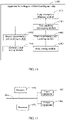
- the method for testing each first preset DFT logic circuit at the RTL stage of the target artificial intelligence chip is different from the method for testing each first preset DFT logic circuit at the synthesis stage in the prior art in that: if the first preset DFT logic circuit fails the test, the first preset DFT logic circuit is modified, and when the test is performed on the modified first preset DFT logic circuit again, the iteration process does not need to be continuously performed between the DFT configuration and test vectors generation, but the test can be continued before the test vectors are executed, to avoid the waste of test time caused by such continuous iteration. As shown in the comparison between the upper and lower parts in FIG. 12 , it can be seen that the test and repair time for the first preset DFT logic circuit is significantly shorter than the test and repair time in the prior art.
- the method further includes: performing a test on at least one second preset DFT logic circuit in the second test logic circuit at the RTL stage of the target artificial intelligence chip; and if the second preset DFT logic circuit fails the test, repairing the second preset DFT logic circuit at the RTL stage of the target artificial intelligence chip.
- the second preset DFT logic circuit may also include: a test protocol IJTAG logic circuit, a memory built-in self-test circuit and boundary scan circuit, an on-chip clock controller, an uncontrollable asynchronous set/reset circuit for flip-flops, a clock analysis circuit for flip-flop scannability, a control logic circuit for memory test, a control logic circuit for IJTAG network scan test, etc.
- the functional design of the arithmetic unit in the artificial intelligence chip is generally stable in an early stage of the chip design, so some second preset DFT logic circuits of the second test logic circuit in the DFT of the corresponding arithmetic unit can be designed and tested at the RTL stage of the target artificial intelligence chip to complete the corresponding test earlier, without having to wait for the entire AI chip to be completed before starting the design and test.
- the principle of testing and repairing the second preset DFT logic circuit is similar to the principle of testing and repairing the first preset DFT logic circuit in the arithmetic unit array, and details are not repeated here.
- the first preset DFT logic circuit and the second preset DFT logic circuit can be designed and tested at the RTL stage of the target artificial intelligence chip to complete the corresponding test earlier, without waiting for the entire AI chip to complete before starting to design and test. And if the first preset DFT logic circuit or the second preset DFT logic circuit fails the test, the first preset DFT logic circuit or the second preset DFT logic circuit is modified, and when the test is performed on the modified first preset DFT logic circuit or the second preset DFT logic circuit again, the iteration process does not need to be continuously performed between the DFT configuration and test vectors generation, but the test can be continued before the test vectors are executed, to avoid the waste of test time caused by such continuous iteration.
- the test and repair time of the first preset DFT logic circuit and the second preset DFT logic circuit can be effectively reduced.
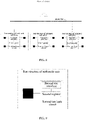
- each black block in FIG. 1 , FIG. 3 , FIG. 6 , FIGS. 8-9 and FIG. 11 represents an arithmetic unit.
- FIG. 13 is a schematic structural diagram of an apparatus for testing an artificial intelligence chip according to the third embodiment of the present application.
- the apparatus for testing an artificial intelligence chip provided in this embodiment is located in an electronic device.
- a target artificial intelligence chip has multiple same arithmetic units, and the apparatus 1300 for testing an artificial intelligence chip includes: a scale information obtaining module 1301, a test condition determining module 1302, an array testing module 1303 and an arithmetic unit testing module 1304.
- the scale information obtaining module 1301 is configured to obtain scale information of the target artificial intelligence chip.
- the test condition determining module 1302 is configured to determine whether the target artificial intelligence chip satisfies a test condition of an arithmetic unit array level according to the scale information.
- the array testing module 1303 is configured to divide all the arithmetic units into multiple same arithmetic unit arrays, and perform a DFT test on the arithmetic unit arrays, respectively, if it is determined that the test condition of the arithmetic unit array level is satisfied.
- the arithmetic unit testing module 1304 is configured to perform the DFT test on the arithmetic units, respectively, if it is determined that the test condition of the arithmetic unit array level is not satisfied.
- the apparatus for testing an artificial intelligence chip provided in this embodiment can execute the technical solution of the method embodiment shown in FIG. 2 , and its implementation principle and technical effects are similar to the method embodiment shown in FIG. 2 , and details are not repeated herein.
- FIG. 14 is a schematic structural diagram of an apparatus for testing an artificial intelligence chip according to the fourth embodiment of the present application.
- the apparatus 1400 for testing an artificial intelligence chip provided in this embodiment based on the apparatus 1300 for testing an artificial intelligence chip provided in the third embodiment of the present application, further includes: a first circuit testing and repairing module 1401 and a second circuit testing and repairing module 1402.
- the scale information includes a number of transistors in an arithmetic unit.
- the test condition determining module 1302 is specifically configured to: determine whether the number of the transistors is smaller than a preset scale threshold; determine the test condition of the arithmetic unit array level is satisfied, if it is determined that the number of the transistors is less than the preset scale threshold; determine the test condition of the arithmetic unit array level is not satisfied, if it is determined that the number of the transistors is greater than or equal to the preset scale threshold.
- the array testing module 1303, when dividing all arithmetic units into multiple same arithmetic unit arrays, is specifically configured to: determine a number of arithmetic units in an arithmetic unit array according to the number of the transistors and the total number of the arithmetic units; divide all the arithmetic units into the multiple same arithmetic unit arrays, according to the number of the arithmetic units.
- each arithmetic unit array is provided with a first test logic circuit.
- the array testing module 1303 is specifically configured to: generate first test vectors corresponding to the arithmetic unit arrays, where the first test vectors corresponding to respective ones of the arithmetic unit arrays are the same; perform the DFT test on the arithmetic unit arrays, respectively, by inputting the first test vectors into first test logic circuits corresponding to respective ones of the arithmetic unit arrays, respectively; output test results corresponding to respective ones of the arithmetic unit arrays.
- the first test logic circuit includes: a first test interface.
- the array testing module 1303 is specifically configured to: perform, through respective first test interfaces, the DFT test on the arithmetic unit arrays in parallel by broadcasting the first test vectors to the first test logic circuits of corresponding arithmetic unit arrays.
- each arithmetic unit is provided with a second test logic circuit.
- the arithmetic unit testing module 1304 is specifically configured to: generate second test vectors corresponding to the arithmetic units, where the second test vector corresponding to respective ones of the arithmetic units are the same; perform the DFT test on the arithmetic units, respectively, by inputting the second test vectors into the second test logic circuits corresponding to respective ones of the arithmetic units, respectively; outputting test results corresponding to respective ones of the arithmetic units.
- the second test logic circuit includes: a second test interface.
- the arithmetic unit testing module 1304 is specifically configured to: perform the DFT test on the arithmetic units in parallel by broadcasting, through respective second test interfaces, the second test vectors to the second test logic circuits of corresponding arithmetic units.
- the first circuit testing and repairing module 1401 is configured to perform a test on at least one first preset DFT logic circuit in the first test logic circuit at an RTL stage of the target artificial intelligence chip; and repair the first preset DFT logic circuit at the RTL stage of the target artificial intelligence chip, if the first preset DFT logic circuit fails the test.
- the second circuit testing and repairing module 1402 is configured to perform a test on at least one second preset DFT logic circuit in the second test logic circuit at the RTL stage of the target artificial intelligence chip; and repair the second preset DFT logic circuit at the RTL stage of the target artificial intelligence chip, if the second preset DFT logic circuit fails the test.
- the apparatus for testing an artificial intelligence chip provided in this embodiment can execute the technical solution of the method embodiment shown in FIG. 4-FIG. 5 , FIG. 7 , FIG. 10 , and its implementation principle and technical effects are similar to the method embodiment shown in FIG. 4-FIG. 5 , FIG. 7 , FIG. 10 , and details are not repeated herein.
- the present application further provides an electronic device and a readable storage medium.
- FIG. 15 it is a block diagram of an electronic device according to the method for testing an artificial intelligence chip according to an embodiment of the present application.
- the electronic device is intended to be various forms of digital computers, such as a laptop computer, a desktop computer, a workstation, a test machine, a personal digital assistant, a server, a blade server, a mainframe computer, and other suitable computers.
- the electronic device can also represent various forms of mobile devices, such as a personal digital assistant, a cellular phone, a smart phone, a wearable device, and other similar computing devices.
- the components shown herein, their connections and relationships, and their functions are merely illustrative, and are not intended to limit the implementation of the application described and/or claimed herein.
- the electronic device includes: one or more processors 1501, a memory 1502, and interfaces for connecting various components, including a high-speed interface and a low-speed interface.
- the various components are connected to each other using different buses and can be installed on a common motherboard or in other ways as needed.
- the processor may process instructions executed within the electronic device, including instructions stored in or on the memory to display graphical information of a GUI on an external input/output equipment, such as a display device coupled to the interface.
- multiple processors and/or multiple buses may be used with multiple memories if desired.
- multiple electronic devices can be connected, and each device provides some necessary operations (for example, as a server array, a group of blade servers, or a multiprocessor system).
- one processor 1501 is taken as an example.
- the memory 1502 is a non-transitory computer-readable storage medium provided by this application.
- the memory stores instructions executable by at least one processor, so that the at least one processor executes the method for testing an artificial intelligence chip provided by the present application.
- the non-transitory computer-readable storage medium of the present application stores computer instructions for causing the computer to execute the method for testing an artificial intelligence chip provided by the present application.
- the memory 1502 can be used to store non-transitory software programs, non-transitory computer executable programs and modules, such as program instructions/modules corresponding to the method for testing an artificial intelligence chip in the embodiments of the present application (e.g. the scale information obtaining module 1301, the test condition determining module 1302, the array testing module 1303, the arithmetic unit testing module 1304 shown in FIG. 13 ).
- the processor 1501 executes various functional applications and data processing of the server by running non-transitory software programs, instructions and modules stored in the memory 1502, that is, implementing the method for testing an artificial intelligence chip in the foregoing method embodiments.
- the memory 1502 may include a program storage area and a data storage area, where the program storage area may store an operating system and application programs required by at least one function and the data storage area may store data created according to the use of the electronic device of FIG. 15 and the like.
- the memory 1502 may include a high-speed random access memory, and may also include a non-transitory memory, such as at least one magnetic disk storage device, a flash memory device, or other non-transitory solid-state storage devices.
- the memory 1502 may optionally include memories remotely provided with respect to the processor 1501, and these remote memories may be connected to the electronic device of FIG. 15 through a network. Examples of the above network include but are not limited to the Internet, an intranet, a local area network, a mobile communication network, and a combination thereof.
- the electronic device of FIG. 15 may further include: an input equipment 1503 and an output equipment 1504.
- the processor 1501, the memory 1502, the input equipment 1503, and the output equipment 1504 may be connected by a bus or other means. In FIG. 15 , the connection by a bus is used as an example.
- the input equipment 1503 such as a touch screen, a keypad, a mouse, a track pad, a touch pad, a pointing stick, one or more mouse buttons, a trackball, a joystick and other input equipment, can receive input voice, numeric or character information, and generate a key signal input related to user setting and function control of the electronic device of FIG. 15 .
- the output equipment 1504 may include a voice playback device, a display device, an auxiliary lighting apparatus (for example, LED), a tactile feedback apparatus (for example, a vibration motor), and the like.
- the display device may include, but is not limited to, a liquid crystal display (LCD), a light emitting diode (LED) display, and a plasma display. In some embodiments, the display device may be a touch screen.
- Various embodiments of the systems and techniques described herein may be implemented in a digital electronic circuitry, an integrated circuit system, a dedicated ASIC (application specific integrated circuit), computer hardware, firmware, software, and/or a combination thereof.
- These various implementations may include: to implement in one or more computer programs that can be executed and/or interpreted on a programmable system that includes at least one programmable processor, where the programmable processor can be a dedicated or general-purpose programmable processor, and can receive data and instructions from a storage system, at least one input equipment, and at least one output equipment, and send data and instructions to the storage system, the at least one input equipment, and the at least one output equipment.
- machine-readable medium and “computer-readable medium” refer to any computer program product, device, and/or apparatus (for example, magnetic disks, optical disks, memory, programmable logic devices (PLD)) used to provide machine instructions and/or data to a programmable processor, including a machine-readable medium that receives the machine instructions as machine-readable signals.
- machine-readable signal refers to any signal used to provide machine instructions and/or data to a programmable processor.
- a computer having display apparatus for displaying information to the user (for example, CRT (Cathode Ray Tube) or LCD (Liquid Crystal Display) monitor), and keyboard and pointing apparatus (for example, mouse or trackball), which the user can use to provide input to the computer.
- display apparatus for displaying information to the user
- keyboard and pointing apparatus for example, mouse or trackball
- Other kinds of devices can also be used to provide interaction with users.
- a feedback provided to the user may be any form of sensory feedback (for example, visual feedback, auditory feedback, or tactile feedback), and an input can be received from the user in any form (including sound input, voice input, or tactile input) .
- the systems and techniques described herein may be implemented in a computing system that includes a back-end component (e.g., as a data server), or a computing system that includes a middleware component (e.g., an application server), or a computing system that includes a front-end component (e.g., a user computer with a graphical user interface or a web browser, through which the user can interact with the implementation of the systems and technologies described herein), or a computing system includes any combination of such background component, middleware component, or front-end component.
- the components of the system can be interconnected by any form or medium of digital data communication (e.g., a communication network). Examples of the communication network includes: a local area network (LAN), a wide area network (WAN) and the Internet.
- the computer system may include a client and a server.
- the client and the server are generally far from each other and usually interact through a communication network.
- the relationship of the client and the server is generated by computer programs that run on corresponding computers and have a client-server relationship with each other.
- the test logic circuit and the test vector of each arithmetic unit array or arithmetic unit are completely the same. So the test cost is reduced.
- the number of the transistors in each arithmetic unit or arithmetic unit array is very small, so that the scale of the test vector is also small, and thus the test time is greatly reduced and the test efficiency is improved.
- loading the DFT of each arithmetic unit or arithmetic unit array will require far less computing and storing resources of the memory, which greatly reduces the test power consumption.
Landscapes
- Engineering & Computer Science (AREA)
- Theoretical Computer Science (AREA)
- Physics & Mathematics (AREA)
- General Engineering & Computer Science (AREA)
- Computer Hardware Design (AREA)
- General Physics & Mathematics (AREA)
- Evolutionary Computation (AREA)
- Geometry (AREA)
- Quality & Reliability (AREA)
- Computational Linguistics (AREA)
- Artificial Intelligence (AREA)
- Data Mining & Analysis (AREA)
- Computing Systems (AREA)
- Mathematical Physics (AREA)
- Software Systems (AREA)
- Tests Of Electronic Circuits (AREA)
- Test And Diagnosis Of Digital Computers (AREA)
- For Increasing The Reliability Of Semiconductor Memories (AREA)
- Techniques For Improving Reliability Of Storages (AREA)
- Thin Film Transistor (AREA)
Claims (15)
- Verfahren zum Testen eines Chips für künstliche Intelligenz, wobei ein Ziel-Chip für künstliche Intelligenz mehrere gleiche arithmetische Einheiten aufweist, und das Verfahren Folgendes umfasst:Erhalten (S101) von Skaleninformationen des Ziel-Chips für künstliche Intelligenz;Bestimmen (S102), ob der Ziel-Chip für künstliche Intelligenz eine Testbedingung einer Arithmetikeinheit-Array-Ebene gemäß den Skaleninformationen erfüllt;Aufteilen (S103) aller arithmetischen Einheiten in mehrere gleiche Arithmetikeinheit-Arrays, und Durchführen eines Testdesign- (Design for Test, DFT) Tests an den jeweiligen Arithmetikeinheit-Arrays in einem Fall, in dem bestimmt wird, dass die Testbedingung der Arithmetikeinheit-Array-Ebene erfüllt ist;Durchführen (S104) des DFT-Tests an den arithmetischen Einheiten, wenn bestimmt wird, dass die Testbedingung der Arithmetikeinheit-Array-Ebene nicht erfüllt ist.
- Verfahren nach Anspruch 1, wobei die Skaleninformationen eine Anzahl von Transistoren in einer arithmetischen Einheit umfassen, und das Bestimmen (S 102), ob der Ziel-Chip für künstliche Intelligenz eine Testbedingung einer Arithmetikeinheit-Array-Ebene gemäß den Skaleninformationen erfüllt, Folgendes umfasst:Bestimmen (S202), ob die Anzahl der Transistoren kleiner als ein voreingestellter Skalenschwellenwert ist;Bestimmen, dass die Testbedingung der Arithmetikeinheit-Array-Ebene erfüllt ist, falls bestimmt wird, dass die Anzahl der Transistoren kleiner als der voreingestellte Skalenschwellenwert ist;Bestimmen, dass die Testbedingung der Arithmetikeinheit-Array-Ebene nicht erfüllt ist, falls bestimmt wird, dass die Anzahl der Transistoren größer oder gleich dem voreingestellten Skalenschwellenwert ist;wobei das Aufteilen (S103) aller arithmetischen Einheiten in mehrere gleiche Arithmetikeinheit-Arrays Folgendes umfasst:Bestimmen (S2031) einer Anzahl von arithmetischen Einheiten in einem Arithmetikeinheit-Array entsprechend der Anzahl der Transistoren und der Gesamtzahl der arithmetischen Einheiten;Aufteilen (S2032) aller arithmetischen Einheiten in mehrere gleiche Arithmetikeinheit-Arrays entsprechend der Anzahl der arithmetischen Einheiten.
- Verfahren nach Anspruch 1, wobei jede der Arithmetikeinheit-Arrays mit einer ersten Testlogikschaltung versehen ist;
wobei das Durchführen (S104) eines DFT-Tests an den Arithmetikeinheit-Arrays jeweils Folgendes umfasst:Erzeugen (S2041) erster Testvektoren, die den Arithmetikeinheit-Arrays entsprechen, wobei die ersten Testvektoren, die den jeweiligen Arithmetikeinheit-Arrays entsprechen, die gleichen sind;Durchführen (S2042) des DFT-Tests an den jeweiligen Arithmetikeinheit-Arrays durch Eingeben der ersten Testvektoren in erste Testlogikschaltungen, die den jeweiligen Arithmetikeinheit-Arrays entsprechen;Ausgeben (S2043) von Testergebnissen entsprechend den jeweiligen Arithmetikeinheit- Arrays;wobei die erste Testlogikschaltung Folgendes umfasst: eine erste Testschnittstelle;das Durchführen (S2042) des DFT-Tests an den jeweiligen Arithmetikeinheit-Arrays durch Eingeben der ersten Testvektoren in erste Testlogikschaltungen, die den jeweiligen Arithmetikeinheit-Arrays entsprechen, Folgendes umfasst:
Durchführen des DFT-Tests an den Arithmetikeinheit-Arrays parallel durch Senden der ersten Testvektoren über jeweilige erste Testschnittstellen an die ersten Testlogikschaltungen der entsprechenden Arithmetikeinheit-Arrays. - Verfahren nach Anspruch 1, wobei jede der Arithmetikeinheiten mit einer zweiten Testlogikschaltung versehen ist;
wobei das Durchführen (S104) des DFT-Tests an den Arithmetikeinheiten jeweils Folgendes umfasst:Erzeugen (S2051) zweiter Testvektoren, die den Arithmetikeinheiten entsprechen, wobei die zweiten Testvektoren, die den jeweiligen Arithmetikeinheiten entsprechen, die gleichen sind;Durchführen (S2052) des DFT-Tests an den jeweiligen Arithmetikeinheiten durch Eingeben der zweiten Testvektoren in zweite Testlogikschaltungen, die den jeweiligen Arithmetikeinheiten entsprechen;Ausgeben (S2053) von Testergebnissen entsprechend den jeweiligen Arithmetikeinheiten;wobei die zweite Testlogikschaltung Folgendes umfasst: eine zweite Testschnittstelle;wobei das Durchführen (S2052) des DFT-Tests an den jeweiligen Arithmetikeinheiten durch Eingeben der zweiten Testvektoren in zweite Testlogikschaltungen, die den jeweiligen Arithmetikeinheiten entsprechen, Folgendes umfasst:
Durchführen des DFT-Tests an den Arithmetikeinheiten parallel durch Senden der zweiten Testvektoren über jeweilige zweite Testschnittstellen an die zweiten Testlogikschaltungen der entsprechenden Arithmetikeinheiten. - Verfahren nach Anspruch 3, wobei das Verfahren vor der Durchführung des DFT-Tests an den jeweiligen Arithmetikeinheit-Arrays ferner Folgendes umfasst:Durchführen eines Tests an mindestens einer ersten voreingestellten DFT-Logikschaltung in der ersten Testlogikschaltung in einer Registerübertragungsebenen-(Register-Transfer-Level, RTL) Stufe des Ziel-Chips für künstliche Intelligenz;Reparieren der ersten voreingestellten DFT-Logikschaltung in der RTL-Stufe des Ziel-Chips für künstliche Intelligenz, falls die erste voreingestellte DFT-Logikschaltung den Test nicht besteht.
- Verfahren nach Anspruch 4, wobei das Verfahren vor der Durchführung des DFT-Tests an den jeweiligen Arithmetikeinheiten ferner Folgendes umfasst:Durchführen eines Tests an mindestens einer zweiten voreingestellten DFT-Logikschaltung in der zweiten Testlogikschaltung in einer RTL-Stufe des Ziel-Chips für künstliche Intelligenz;Reparieren der zweiten voreingestellten DFT-Logikschaltung in der RTL-Stufe des Ziel-Chips für künstliche Intelligenz, falls die zweite voreingestellte DFT-Logikschaltung den Test nicht besteht.
- Vorrichtung (1300) zum Testen eines Chips für künstliche Intelligenz, wobei ein Ziel-Chip für künstliche Intelligenz mehrere gleiche arithmetische Einheiten aufweist, und die Vorrichtung Folgendes umfasst:ein Modul (1301) zur Gewinnung von Skaleninformationen, das dafür konfiguriert ist, Skaleninformationen des Ziel-Chips für künstliche Intelligenz zu erhalten;ein Testbedingungs-Bestimmungsmodul (1302), das dafür konfiguriert ist, zu bestimmen, ob der Ziel-Chip für künstliche Intelligenz eine Testbedingung einer Arithmetikeinheit-Array-Ebene gemäß den Skaleninformationen erfüllt;ein Array-Testmodul (1303), das dafür konfiguriert ist, alle arithmetischen Einheiten in mehrere gleiche Arrays von arithmetischen Einheiten zu unterteilen und einen Testdesign-(DFT) Test an den Arrays von arithmetischen Einheiten durchzuführen, in einem Fall, in dem bestimmt wird, dass die Testbedingung der Arithmetikeinheit-Array-Ebene erfüllt ist;ein Arithmetikeinheit-Testmodul (1304), das dafür konfiguriert ist, den DFT-Test an den arithmetischen Einheiten durchzuführen, wenn bestimmt wird, dass die Testbedingung der Arithmetikeinheit-Array-Ebene nicht erfüllt ist.
- Vorrichtung (1300) nach Anspruch 7, wobei die Skaleninformationen eine Anzahl von Transistoren in einer arithmetischen Einheit umfassen, und
das Testbedingungs-Bestimmungsmodul (1302) speziell für Folgendes konfiguriert ist:
Bestimmen, ob die Anzahl der Transistoren kleiner als ein voreingestellter Skalenschwellenwert ist; Bestimmen, dass die Testbedingung der Arithmetikeinheit-Array-Ebene erfüllt ist, falls bestimmt wird, dass die Anzahl der Transistoren kleiner als der voreingestellte Skalenschwellenwert ist; Bestimmen, dass die Testbedingung der Arithmetikeinheit-Array-Ebene nicht erfüllt ist, falls bestimmt wird, dass die Anzahl der Transistoren größer oder gleich dem voreingestellten Skalenschwellenwert ist. - Vorrichtung (1300) nach Anspruch 8, wobei beim Aufteilen aller Arithmetikeinheiten in mehrere gleiche Arithmetikeinheit-Arrays das Array-Testmodul (1303) speziell für Folgendes konfiguriert ist:
Bestimmen einer Anzahl von arithmetischen Einheiten in einem Arithmetikeinheit-Array entsprechend der Anzahl der Transistoren und der Gesamtzahl der arithmetischen Einheiten; und Aufteilen aller arithmetischen Einheiten in mehrere gleiche Arithmetikeinheit-Arrays entsprechend der Anzahl der arithmetischen Einheiten. - Vorrichtung (1300) nach Anspruch 7, wobei jede der Arithmetikeinheit-Arrays mit einer ersten Testlogikschaltung versehen ist;
wobei, wenn der DFT-Test an den Arithmetikeinheit-Arrays durchgeführt wird, das Array-Testmodul (1303) speziell für Folgendes konfiguriert ist:
Erzeugen erster Testvektoren, die den Arithmetikeinheit-Arrays entsprechen, wobei die ersten Testvektoren, die den jeweiligen Arithmetikeinheit-Arrays entsprechen, die gleichen sind; Durchführen des DFT-Tests an den jeweiligen Arithmetikeinheit-Arrays durch Eingeben der ersten Testvektoren in erste Testlogikschaltungen, die den jeweiligen Arithmetikeinheit-Arrays entsprechen; Ausgeben von Testergebnissen entsprechend den jeweiligen Arithmetikeinheit-Arrays. - Vorrichtung (1300) nach Anspruch 10, wobei die erste Testlogikschaltung Folgendes umfasst: eine erste Testschnittstelle;
wobei, wenn der DFT-Test an den Arithmetikeinheit-Arrays jeweils durch Eingabe der ersten Testvektoren in die ersten Testlogikschaltungen, die jeweils den Arithmetikeinheit-Arrays entsprechen, durchgeführt wird, das Array-Testmodul (1303) speziell für Folgendes konfiguriert ist:
Durchführen des DFT-Tests an den Arithmetikeinheit-Arrays parallel durch Senden der ersten Testvektoren über jeweilige erste Testschnittstellen an die ersten Testlogikschaltungen der entsprechenden Arithmetikeinheit-Arrays. - Vorrichtung (1300) nach Anspruch 7, wobei jede der Arithmetikeinheiten mit einer zweiten Testlogikschaltung versehen ist;
wobei, wenn der DFT-Test an den jeweiligen arithmetischen Einheiten durchgeführt wird, das Arithmetikeinheit-Testmodul (1304) speziell für Folgendes konfiguriert ist:
Erzeugen zweiter Testvektoren, die den Arithmetikeinheiten entsprechen, wobei die zweiten Testvektoren, die den jeweiligen Arithmetikeinheiten entsprechen, die gleichen sind; Durchführen des DFT-Tests an den jeweiligen Arithmetikeinheiten durch Eingeben der zweiten Testvektoren in zweite Testlogikschaltungen, die den jeweiligen Arithmetikeinheiten entsprechen; und Ausgeben von Testergebnissen entsprechend den jeweiligen Arithmetikeinheiten. - Vorrichtung (1300) nach Anspruch 12, wobei die zweite Testlogikschaltung Folgendes umfasst: eine zweite Testschnittstelle;
wobei, wenn der DFT-Test an den Arithmetikeinheiten jeweils durch Eingabe der zweiten Testvektoren in die zweiten Testlogikschaltungen, die jeweils den Arithmetikeinheiten entsprechen, durchgeführt wird, das Arithmetikeinheiten-Testmodul (1304) speziell für Folgendes konfiguriert ist:
Durchführen des DFT-Tests an den Arithmetikeinheiten parallel durch Senden der zweiten Testvektoren über jeweilige zweite Testschnittstellen an die zweiten Testlogikschaltungen der entsprechenden Arithmetikeinheiten. - Vorrichtung (1300) nach Anspruch 10, die ferner Folgendes umfasst:
ein erstes Schaltungstest- und Reparaturmodul (1401), das für Folgendes konfiguriert ist: Durchführen eines Test an mindestens einer ersten voreingestellten DFT-Logikschaltung in der ersten Testlogikschaltung in einer Registerübertragungsebenen-, RTL, Stufe des Ziel-Chips für künstliche Intelligenz; und Reparieren der ersten voreingestellten DFT-Logikschaltung in der RTL-Stufe des Ziel-Chips für künstliche Intelligenz, falls die erste voreingestellte DFT-Logikschaltung den Test nicht besteht. - Vorrichtung (1300) nach Anspruch 12, die ferner Folgendes umfasst:
ein zweites Schaltungstest- und Reparaturmodul (1402), das für Folgendes konfiguriert ist: Durchführen eines Test an mindestens einer zweiten voreingestellten DFT-Logikschaltung in der zweiten Testlogikschaltung in einer RTL-Stufe des Ziel-Chips für künstliche Intelligenz; und Reparieren der zweiten voreingestellten DFT-Logikschaltung in der RTL-Stufe des Ziel-Chips für künstliche Intelligenz, falls die zweite voreingestellte DFT-Logikschaltung den Test nicht besteht.
Applications Claiming Priority (1)
| Application Number | Priority Date | Filing Date | Title |
|---|---|---|---|
| CN201911420462.8A CN111158967B (zh) | 2019-12-31 | 2019-12-31 | 人工智能芯片测试方法、装置、设备及存储介质 |
Publications (3)
| Publication Number | Publication Date |
|---|---|
| EP3812908A2 EP3812908A2 (de) | 2021-04-28 |
| EP3812908A3 EP3812908A3 (de) | 2021-05-26 |
| EP3812908B1 true EP3812908B1 (de) | 2022-10-05 |
Family
ID=70560453
Family Applications (1)
| Application Number | Title | Priority Date | Filing Date |
|---|---|---|---|
| EP20204930.0A Active EP3812908B1 (de) | 2019-12-31 | 2020-10-30 | Verfahren und vorrichtung zum testen eines chips zur verwendung in künstlicher intelligenz, vorrichtung und speichermedium |
Country Status (5)
| Country | Link |
|---|---|
| US (1) | US11714128B2 (de) |
| EP (1) | EP3812908B1 (de) |
| JP (1) | JP7029873B2 (de) |
| KR (1) | KR102374380B1 (de) |
| CN (1) | CN111158967B (de) |
Families Citing this family (13)
| Publication number | Priority date | Publication date | Assignee | Title |
|---|---|---|---|---|
| CN111833959B (zh) * | 2020-07-20 | 2022-08-02 | 北京百度网讯科技有限公司 | 存储器的测试的方法、装置、电子设备和计算机可读存储介质 |
| US11988709B2 (en) * | 2020-12-31 | 2024-05-21 | Deepx Co., Ltd. | System capable of detecting failure of component of system and method thereof |
| CN112881887B (zh) * | 2021-01-15 | 2023-02-17 | 深圳比特微电子科技有限公司 | 芯片测试方法和计算芯片 |
| CN112968948A (zh) * | 2021-02-01 | 2021-06-15 | 中国第一汽车股份有限公司 | 一种网关控制器的设计方法、网关控制器及汽车 |
| CN113568821B (zh) * | 2021-07-26 | 2024-10-29 | 昆仑芯(北京)科技有限公司 | 一种ai芯片计算性能的测试方法、装置、设备、及介质 |
| CN118020033A (zh) * | 2021-09-26 | 2024-05-10 | 华为技术有限公司 | 人工智能芯片的控制方法和相关装置 |
| CN113779913B (zh) * | 2021-11-12 | 2022-03-22 | 浙江大学 | 一种面向ai多芯片系统的验证平台结构和测试方法 |
| CN115268406B (zh) * | 2022-07-29 | 2023-09-29 | 江苏芯安集成电路设计有限公司 | 一种单片机芯片测试方法、系统、计算机设备及存储介质 |
| CN115267513B (zh) * | 2022-08-25 | 2025-07-11 | 深圳市华力宇电子科技有限公司 | 基于集成电路测试机测试芯片故障的方法、系统及设备 |
| CN117783809A (zh) * | 2022-09-22 | 2024-03-29 | 深圳市中兴微电子技术有限公司 | 芯片测试方法、装置、芯片及计算机可读存储介质 |
| CN115716277A (zh) * | 2022-11-28 | 2023-02-28 | 内江师范学院 | 一种用于工业机器人姿态测评方法及系统 |
| CN117112328B (zh) * | 2023-08-07 | 2025-11-14 | 合肥智能语音创新发展有限公司 | Npu测试方法及相关装置、设备和存储介质 |
| CN117538727B (zh) * | 2023-10-31 | 2025-05-13 | 汕头大学 | 面向异构计算的并行故障模拟方法、系统和介质 |
Family Cites Families (20)
| Publication number | Priority date | Publication date | Assignee | Title |
|---|---|---|---|---|
| US5822557A (en) * | 1991-12-27 | 1998-10-13 | Fujitsu Limited | Pipelined data processing device having improved hardware control over an arithmetic operations unit |
| JP4490366B2 (ja) * | 2005-12-13 | 2010-06-23 | 富士通株式会社 | リソース割当て方法及び,これを用いた演算回路の診断システム |
| JPWO2008069025A1 (ja) * | 2006-11-29 | 2010-03-18 | 日本電気株式会社 | 半導体装置 |
| CN101751317B (zh) | 2008-12-12 | 2013-11-20 | 上海芯豪微电子有限公司 | 多运算单元/多核/众核系统的自测试自修复机制与结构 |
| KR101742590B1 (ko) * | 2010-05-05 | 2017-06-01 | 테라다인 인코퍼레이티드 | 반도체 장치들의 동시 시험을 위한 시스템 |
| KR101912427B1 (ko) * | 2011-12-12 | 2018-10-29 | 삼성전자주식회사 | 재구성가능 프로세서 및 재구성가능 프로세서의 미니 코어 |
| US9423455B2 (en) * | 2014-12-15 | 2016-08-23 | Genesys Testware, Inc. | Design-for-test techniques for a digital electronic circuit |
| US20170045579A1 (en) * | 2015-08-14 | 2017-02-16 | Texas Instruments Incorporated | Cpu bist testing of integrated circuits using serial wire debug |
| CN105138440B (zh) * | 2015-09-24 | 2017-09-12 | 北京工业大学 | 一种自带对比功能的标准单元库功能测试方法 |
| US10347317B2 (en) * | 2017-10-05 | 2019-07-09 | Gyrfalcon Technology Inc. | Method of self-testing and reusing of reference cells in a memory architecture |
| US10523209B1 (en) * | 2017-11-14 | 2019-12-31 | Flex Logix Technologies, Inc. | Test circuitry and techniques for logic tiles of FPGA |
| CN109978152B (zh) * | 2017-12-27 | 2020-05-22 | 中科寒武纪科技股份有限公司 | 集成电路芯片装置及相关产品 |
| CN109376041A (zh) * | 2018-09-19 | 2019-02-22 | 广州优亿信息科技有限公司 | 一种用于ai手机芯片的基准测试系统及其工作流程 |
| CN109358993A (zh) | 2018-09-26 | 2019-02-19 | 中科物栖(北京)科技有限责任公司 | 深度神经网络加速器故障的处理方法及装置 |
| CN109634843B (zh) * | 2018-10-31 | 2021-09-21 | 中国科学院软件研究所 | 一种面向ai芯片平台的分布式自动化软件测试方法及平台 |
| US10691372B1 (en) * | 2018-12-07 | 2020-06-23 | Western Digital Technologies, Inc. | Transistor threshold voltage maintenance in 3D memory |
| CN109919322B (zh) * | 2019-02-01 | 2022-01-28 | 京微齐力(北京)科技有限公司 | 一种测试系统芯片上的人工智能模块的方法和系统芯片 |
| CN109884499B (zh) * | 2019-02-01 | 2022-04-15 | 京微齐力(北京)科技有限公司 | 一种测试系统芯片上的人工智能模块的方法和系统芯片 |
| CN109765482A (zh) | 2019-03-11 | 2019-05-17 | 世芯电子科技(无锡)有限公司 | 一种多芯片间高速互连测试方法 |
| CN110489861A (zh) * | 2019-08-19 | 2019-11-22 | 福建工程学院 | 一种ai边缘运算芯片设计的弹性实现方法 |
-
2019
- 2019-12-31 CN CN201911420462.8A patent/CN111158967B/zh active Active
-
2020
- 2020-05-14 JP JP2020085123A patent/JP7029873B2/ja active Active
- 2020-05-21 KR KR1020200060686A patent/KR102374380B1/ko active Active
- 2020-09-15 US US17/021,080 patent/US11714128B2/en active Active
- 2020-10-30 EP EP20204930.0A patent/EP3812908B1/de active Active
Also Published As
| Publication number | Publication date |
|---|---|
| KR102374380B1 (ko) | 2022-03-15 |
| US20210223311A1 (en) | 2021-07-22 |
| JP2021081413A (ja) | 2021-05-27 |
| EP3812908A3 (de) | 2021-05-26 |
| EP3812908A2 (de) | 2021-04-28 |
| CN111158967B (zh) | 2021-06-08 |
| JP7029873B2 (ja) | 2022-03-04 |
| KR20210038288A (ko) | 2021-04-07 |
| US11714128B2 (en) | 2023-08-01 |
| CN111158967A (zh) | 2020-05-15 |
Similar Documents
| Publication | Publication Date | Title |
|---|---|---|
| EP3812908B1 (de) | Verfahren und vorrichtung zum testen eines chips zur verwendung in künstlicher intelligenz, vorrichtung und speichermedium | |
| EP3943960B1 (de) | Verfahren und vorrichtung zum testen eines chips, und zugehöriger chip | |
| CN113514759B (zh) | 一种多核测试处理器及集成电路测试系统与方法 | |
| CN111833959B (zh) | 存储器的测试的方法、装置、电子设备和计算机可读存储介质 | |
| CN117193986A (zh) | 一种多线程处理方法、装置、计算机设备及存储介质 | |
| He et al. | Fecaffe: Fpga-enabled caffe with opencl for deep learning training and inference on intel stratix 10 | |
| CN113868999A (zh) | 芯片优化系统及方法 | |
| US7657851B2 (en) | Device, system, and method for correction of integrated circuit design | |
| US12572727B2 (en) | Static timing analysis method and static timing analysis system | |
| Odetola et al. | 2l-3w: 2-level 3-way hardware-software co-verification for the mapping of deep learning architecture (dla) onto fpga boards | |
| US11048844B1 (en) | System and method for use in design verification | |
| CN110442986B (zh) | 一种基于cpld逻辑代码生成器管理服务器主板的方法 | |
| Liu et al. | A GPU-accelerated parallel shooting algorithm for analysis of radio frequency and microwave integrated circuits | |
| US8285527B2 (en) | Method and system for equivalence checking | |
| US7305636B2 (en) | Method and system for formal unidirectional bus verification using synthesizing constrained drivers | |
| US8938705B1 (en) | Systems and methods for partial retention synthesis | |
| US11449337B1 (en) | Pseudorandom keephot instructions to mitigate large load steps during hardware emulation | |
| JP6473023B2 (ja) | 性能評価モジュール及びこれを組み込んだ半導体集積回路 | |
| US12014205B2 (en) | Advanced register merging | |
| US20250356092A1 (en) | Method and apparatus for testing circuit based on test coverage optimization | |
| Zhao et al. | SoCDev: SoC Design Automation through TCL Code Generation via LLM-Based Agents | |
| KR20250111265A (ko) | 명령어 실행 장치, 방법, 전자 기기, 저장 매체 및 컴퓨터 프로그램 | |
| Rachamalla et al. | Virtual logic netlist: Enabling efficient RTL analysis | |
| CN119067021A (zh) | 一种芯片约束和综合的实现方法、装置、设备及介质 | |
| CN115730508A (zh) | 使用设计和辅助构造的基于监督机器学习的存储器和运行时间预测 |
Legal Events
| Date | Code | Title | Description |
|---|---|---|---|
| PUAI | Public reference made under article 153(3) epc to a published international application that has entered the european phase |
Free format text: ORIGINAL CODE: 0009012 |
|
| STAA | Information on the status of an ep patent application or granted ep patent |
Free format text: STATUS: REQUEST FOR EXAMINATION WAS MADE |
|
| PUAL | Search report despatched |
Free format text: ORIGINAL CODE: 0009013 |
|
| 17P | Request for examination filed |
Effective date: 20201030 |
|
| AK | Designated contracting states |
Kind code of ref document: A2 Designated state(s): AL AT BE BG CH CY CZ DE DK EE ES FI FR GB GR HR HU IE IS IT LI LT LU LV MC MK MT NL NO PL PT RO RS SE SI SK SM TR |
|
| AX | Request for extension of the european patent |
Extension state: BA ME |
|
| AK | Designated contracting states |
Kind code of ref document: A3 Designated state(s): AL AT BE BG CH CY CZ DE DK EE ES FI FR GB GR HR HU IE IS IT LI LT LU LV MC MK MT NL NO PL PT RO RS SE SI SK SM TR |
|
| RIC1 | Information provided on ipc code assigned before grant |
Ipc: G06F 11/22 20060101AFI20210421BHEP |
|
| RAP3 | Party data changed (applicant data changed or rights of an application transferred) |
Owner name: BEIJING BAIDU NETCOM SCIENCE TECHNOLOGY CO., LTD. |
|
| RAP1 | Party data changed (applicant data changed or rights of an application transferred) |
Owner name: KUNLUNXIN TECHNOLOGY (BEIJING) COMPANY LIMITED |
|
| RAP1 | Party data changed (applicant data changed or rights of an application transferred) |
Owner name: KUNLUNXIN TECHNOLOGY (BEIJING) COMPANY LIMITED Owner name: BEIJING BAIDU NETCOM SCIENCE AND TECHNOLOGY CO., LTD. |
|
| GRAP | Despatch of communication of intention to grant a patent |
Free format text: ORIGINAL CODE: EPIDOSNIGR1 |
|
| STAA | Information on the status of an ep patent application or granted ep patent |
Free format text: STATUS: GRANT OF PATENT IS INTENDED |
|
| INTG | Intention to grant announced |
Effective date: 20220719 |
|
| GRAS | Grant fee paid |
Free format text: ORIGINAL CODE: EPIDOSNIGR3 |
|
| GRAA | (expected) grant |
Free format text: ORIGINAL CODE: 0009210 |
|
| STAA | Information on the status of an ep patent application or granted ep patent |
Free format text: STATUS: THE PATENT HAS BEEN GRANTED |
|
| AK | Designated contracting states |
Kind code of ref document: B1 Designated state(s): AL AT BE BG CH CY CZ DE DK EE ES FI FR GB GR HR HU IE IS IT LI LT LU LV MC MK MT NL NO PL PT RO RS SE SI SK SM TR |
|
| REG | Reference to a national code |
Ref country code: GB Ref legal event code: FG4D |
|
| REG | Reference to a national code |
Ref country code: CH Ref legal event code: EP |
|
| REG | Reference to a national code |
Ref country code: AT Ref legal event code: REF Ref document number: 1523173 Country of ref document: AT Kind code of ref document: T Effective date: 20221015 |
|
| REG | Reference to a national code |
Ref country code: IE Ref legal event code: FG4D |
|
| REG | Reference to a national code |
Ref country code: DE Ref legal event code: R096 Ref document number: 602020005472 Country of ref document: DE |
|
| REG | Reference to a national code |
Ref country code: LT Ref legal event code: MG9D |
|
| REG | Reference to a national code |
Ref country code: NL Ref legal event code: MP Effective date: 20221005 |
|
| REG | Reference to a national code |
Ref country code: AT Ref legal event code: MK05 Ref document number: 1523173 Country of ref document: AT Kind code of ref document: T Effective date: 20221005 |
|
| PG25 | Lapsed in a contracting state [announced via postgrant information from national office to epo] |
Ref country code: NL Free format text: LAPSE BECAUSE OF FAILURE TO SUBMIT A TRANSLATION OF THE DESCRIPTION OR TO PAY THE FEE WITHIN THE PRESCRIBED TIME-LIMIT Effective date: 20221005 |
|
| PG25 | Lapsed in a contracting state [announced via postgrant information from national office to epo] |
Ref country code: SE Free format text: LAPSE BECAUSE OF FAILURE TO SUBMIT A TRANSLATION OF THE DESCRIPTION OR TO PAY THE FEE WITHIN THE PRESCRIBED TIME-LIMIT Effective date: 20221005 Ref country code: PT Free format text: LAPSE BECAUSE OF FAILURE TO SUBMIT A TRANSLATION OF THE DESCRIPTION OR TO PAY THE FEE WITHIN THE PRESCRIBED TIME-LIMIT Effective date: 20230206 Ref country code: NO Free format text: LAPSE BECAUSE OF FAILURE TO SUBMIT A TRANSLATION OF THE DESCRIPTION OR TO PAY THE FEE WITHIN THE PRESCRIBED TIME-LIMIT Effective date: 20230105 Ref country code: LT Free format text: LAPSE BECAUSE OF FAILURE TO SUBMIT A TRANSLATION OF THE DESCRIPTION OR TO PAY THE FEE WITHIN THE PRESCRIBED TIME-LIMIT Effective date: 20221005 Ref country code: FI Free format text: LAPSE BECAUSE OF FAILURE TO SUBMIT A TRANSLATION OF THE DESCRIPTION OR TO PAY THE FEE WITHIN THE PRESCRIBED TIME-LIMIT Effective date: 20221005 Ref country code: ES Free format text: LAPSE BECAUSE OF FAILURE TO SUBMIT A TRANSLATION OF THE DESCRIPTION OR TO PAY THE FEE WITHIN THE PRESCRIBED TIME-LIMIT Effective date: 20221005 Ref country code: AT Free format text: LAPSE BECAUSE OF FAILURE TO SUBMIT A TRANSLATION OF THE DESCRIPTION OR TO PAY THE FEE WITHIN THE PRESCRIBED TIME-LIMIT Effective date: 20221005 |
|
| PG25 | Lapsed in a contracting state [announced via postgrant information from national office to epo] |
Ref country code: RS Free format text: LAPSE BECAUSE OF FAILURE TO SUBMIT A TRANSLATION OF THE DESCRIPTION OR TO PAY THE FEE WITHIN THE PRESCRIBED TIME-LIMIT Effective date: 20221005 Ref country code: PL Free format text: LAPSE BECAUSE OF FAILURE TO SUBMIT A TRANSLATION OF THE DESCRIPTION OR TO PAY THE FEE WITHIN THE PRESCRIBED TIME-LIMIT Effective date: 20221005 Ref country code: LV Free format text: LAPSE BECAUSE OF FAILURE TO SUBMIT A TRANSLATION OF THE DESCRIPTION OR TO PAY THE FEE WITHIN THE PRESCRIBED TIME-LIMIT Effective date: 20221005 Ref country code: IS Free format text: LAPSE BECAUSE OF FAILURE TO SUBMIT A TRANSLATION OF THE DESCRIPTION OR TO PAY THE FEE WITHIN THE PRESCRIBED TIME-LIMIT Effective date: 20230205 Ref country code: HR Free format text: LAPSE BECAUSE OF FAILURE TO SUBMIT A TRANSLATION OF THE DESCRIPTION OR TO PAY THE FEE WITHIN THE PRESCRIBED TIME-LIMIT Effective date: 20221005 Ref country code: GR Free format text: LAPSE BECAUSE OF FAILURE TO SUBMIT A TRANSLATION OF THE DESCRIPTION OR TO PAY THE FEE WITHIN THE PRESCRIBED TIME-LIMIT Effective date: 20230106 |
|
| REG | Reference to a national code |
Ref country code: BE Ref legal event code: MM Effective date: 20221031 |
|
| PG25 | Lapsed in a contracting state [announced via postgrant information from national office to epo] |
Ref country code: LU Free format text: LAPSE BECAUSE OF NON-PAYMENT OF DUE FEES Effective date: 20221030 |
|
| REG | Reference to a national code |
Ref country code: DE Ref legal event code: R097 Ref document number: 602020005472 Country of ref document: DE |
|
| P01 | Opt-out of the competence of the unified patent court (upc) registered |
Effective date: 20230530 |
|
| PG25 | Lapsed in a contracting state [announced via postgrant information from national office to epo] |
Ref country code: SM Free format text: LAPSE BECAUSE OF FAILURE TO SUBMIT A TRANSLATION OF THE DESCRIPTION OR TO PAY THE FEE WITHIN THE PRESCRIBED TIME-LIMIT Effective date: 20221005 Ref country code: RO Free format text: LAPSE BECAUSE OF FAILURE TO SUBMIT A TRANSLATION OF THE DESCRIPTION OR TO PAY THE FEE WITHIN THE PRESCRIBED TIME-LIMIT Effective date: 20221005 Ref country code: MC Free format text: LAPSE BECAUSE OF FAILURE TO SUBMIT A TRANSLATION OF THE DESCRIPTION OR TO PAY THE FEE WITHIN THE PRESCRIBED TIME-LIMIT Effective date: 20221005 Ref country code: EE Free format text: LAPSE BECAUSE OF FAILURE TO SUBMIT A TRANSLATION OF THE DESCRIPTION OR TO PAY THE FEE WITHIN THE PRESCRIBED TIME-LIMIT Effective date: 20221005 Ref country code: DK Free format text: LAPSE BECAUSE OF FAILURE TO SUBMIT A TRANSLATION OF THE DESCRIPTION OR TO PAY THE FEE WITHIN THE PRESCRIBED TIME-LIMIT Effective date: 20221005 Ref country code: CZ Free format text: LAPSE BECAUSE OF FAILURE TO SUBMIT A TRANSLATION OF THE DESCRIPTION OR TO PAY THE FEE WITHIN THE PRESCRIBED TIME-LIMIT Effective date: 20221005 |
|
| PLBE | No opposition filed within time limit |
Free format text: ORIGINAL CODE: 0009261 |
|
| STAA | Information on the status of an ep patent application or granted ep patent |
Free format text: STATUS: NO OPPOSITION FILED WITHIN TIME LIMIT |
|
| PG25 | Lapsed in a contracting state [announced via postgrant information from national office to epo] |
Ref country code: SK Free format text: LAPSE BECAUSE OF FAILURE TO SUBMIT A TRANSLATION OF THE DESCRIPTION OR TO PAY THE FEE WITHIN THE PRESCRIBED TIME-LIMIT Effective date: 20221005 Ref country code: AL Free format text: LAPSE BECAUSE OF FAILURE TO SUBMIT A TRANSLATION OF THE DESCRIPTION OR TO PAY THE FEE WITHIN THE PRESCRIBED TIME-LIMIT Effective date: 20221005 |
|
| 26N | No opposition filed |
Effective date: 20230706 |
|
| PG25 | Lapsed in a contracting state [announced via postgrant information from national office to epo] |
Ref country code: BE Free format text: LAPSE BECAUSE OF NON-PAYMENT OF DUE FEES Effective date: 20221031 |
|
| PG25 | Lapsed in a contracting state [announced via postgrant information from national office to epo] |
Ref country code: IE Free format text: LAPSE BECAUSE OF NON-PAYMENT OF DUE FEES Effective date: 20221030 |
|
| PG25 | Lapsed in a contracting state [announced via postgrant information from national office to epo] |
Ref country code: SI Free format text: LAPSE BECAUSE OF FAILURE TO SUBMIT A TRANSLATION OF THE DESCRIPTION OR TO PAY THE FEE WITHIN THE PRESCRIBED TIME-LIMIT Effective date: 20221005 Ref country code: FR Free format text: LAPSE BECAUSE OF NON-PAYMENT OF DUE FEES Effective date: 20221205 |
|
| PG25 | Lapsed in a contracting state [announced via postgrant information from national office to epo] |
Ref country code: CY Free format text: LAPSE BECAUSE OF FAILURE TO SUBMIT A TRANSLATION OF THE DESCRIPTION OR TO PAY THE FEE WITHIN THE PRESCRIBED TIME-LIMIT Effective date: 20221005 |
|
| PG25 | Lapsed in a contracting state [announced via postgrant information from national office to epo] |
Ref country code: MK Free format text: LAPSE BECAUSE OF FAILURE TO SUBMIT A TRANSLATION OF THE DESCRIPTION OR TO PAY THE FEE WITHIN THE PRESCRIBED TIME-LIMIT Effective date: 20221005 Ref country code: IT Free format text: LAPSE BECAUSE OF FAILURE TO SUBMIT A TRANSLATION OF THE DESCRIPTION OR TO PAY THE FEE WITHIN THE PRESCRIBED TIME-LIMIT Effective date: 20221005 |
|
| REG | Reference to a national code |
Ref country code: CH Ref legal event code: PL |
|
| PG25 | Lapsed in a contracting state [announced via postgrant information from national office to epo] |
Ref country code: CH Free format text: LAPSE BECAUSE OF NON-PAYMENT OF DUE FEES Effective date: 20231031 |
|
| PG25 | Lapsed in a contracting state [announced via postgrant information from national office to epo] |
Ref country code: HU Free format text: LAPSE BECAUSE OF FAILURE TO SUBMIT A TRANSLATION OF THE DESCRIPTION OR TO PAY THE FEE WITHIN THE PRESCRIBED TIME-LIMIT; INVALID AB INITIO Effective date: 20201030 Ref country code: CH Free format text: LAPSE BECAUSE OF NON-PAYMENT OF DUE FEES Effective date: 20231031 Ref country code: BG Free format text: LAPSE BECAUSE OF FAILURE TO SUBMIT A TRANSLATION OF THE DESCRIPTION OR TO PAY THE FEE WITHIN THE PRESCRIBED TIME-LIMIT Effective date: 20221005 |
|
| PG25 | Lapsed in a contracting state [announced via postgrant information from national office to epo] |
Ref country code: MT Free format text: LAPSE BECAUSE OF FAILURE TO SUBMIT A TRANSLATION OF THE DESCRIPTION OR TO PAY THE FEE WITHIN THE PRESCRIBED TIME-LIMIT Effective date: 20221005 |
|
| PGFP | Annual fee paid to national office [announced via postgrant information from national office to epo] |
Ref country code: GB Payment date: 20250911 Year of fee payment: 6 |
|
| PG25 | Lapsed in a contracting state [announced via postgrant information from national office to epo] |
Ref country code: TR Free format text: LAPSE BECAUSE OF FAILURE TO SUBMIT A TRANSLATION OF THE DESCRIPTION OR TO PAY THE FEE WITHIN THE PRESCRIBED TIME-LIMIT Effective date: 20221005 |
|
| PGFP | Annual fee paid to national office [announced via postgrant information from national office to epo] |
Ref country code: DE Payment date: 20250910 Year of fee payment: 6 |