EP3812352B1 - Glasverbundanordnung - Google Patents
Glasverbundanordnung Download PDFInfo
- Publication number
- EP3812352B1 EP3812352B1 EP19205115.9A EP19205115A EP3812352B1 EP 3812352 B1 EP3812352 B1 EP 3812352B1 EP 19205115 A EP19205115 A EP 19205115A EP 3812352 B1 EP3812352 B1 EP 3812352B1
- Authority
- EP
- European Patent Office
- Prior art keywords
- enclosure
- laser
- weld line
- laser weld
- stress
- Prior art date
- Legal status (The legal status is an assumption and is not a legal conclusion. Google has not performed a legal analysis and makes no representation as to the accuracy of the status listed.)
- Active
Links
Images


Classifications
-
- B—PERFORMING OPERATIONS; TRANSPORTING
- B23—MACHINE TOOLS; METAL-WORKING NOT OTHERWISE PROVIDED FOR
- B23K—SOLDERING OR UNSOLDERING; WELDING; CLADDING OR PLATING BY SOLDERING OR WELDING; CUTTING BY APPLYING HEAT LOCALLY, e.g. FLAME CUTTING; WORKING BY LASER BEAM
- B23K26/00—Working by laser beam, e.g. welding, cutting or boring
- B23K26/20—Bonding
- B23K26/21—Bonding by welding
- B23K26/22—Spot welding
-
- B—PERFORMING OPERATIONS; TRANSPORTING
- B23—MACHINE TOOLS; METAL-WORKING NOT OTHERWISE PROVIDED FOR
- B23K—SOLDERING OR UNSOLDERING; WELDING; CLADDING OR PLATING BY SOLDERING OR WELDING; CUTTING BY APPLYING HEAT LOCALLY, e.g. FLAME CUTTING; WORKING BY LASER BEAM
- B23K26/00—Working by laser beam, e.g. welding, cutting or boring
- B23K26/20—Bonding
- B23K26/21—Bonding by welding
-
- B—PERFORMING OPERATIONS; TRANSPORTING
- B23—MACHINE TOOLS; METAL-WORKING NOT OTHERWISE PROVIDED FOR
- B23K—SOLDERING OR UNSOLDERING; WELDING; CLADDING OR PLATING BY SOLDERING OR WELDING; CUTTING BY APPLYING HEAT LOCALLY, e.g. FLAME CUTTING; WORKING BY LASER BEAM
- B23K26/00—Working by laser beam, e.g. welding, cutting or boring
- B23K26/02—Positioning or observing the workpiece, e.g. with respect to the point of impact; Aligning, aiming or focusing the laser beam
- B23K26/06—Shaping the laser beam, e.g. by masks or multi-focusing
- B23K26/0604—Shaping the laser beam, e.g. by masks or multi-focusing by a combination of beams
- B23K26/0608—Shaping the laser beam, e.g. by masks or multi-focusing by a combination of beams in the same heat affected zone [HAZ]
-
- B—PERFORMING OPERATIONS; TRANSPORTING
- B23—MACHINE TOOLS; METAL-WORKING NOT OTHERWISE PROVIDED FOR
- B23K—SOLDERING OR UNSOLDERING; WELDING; CLADDING OR PLATING BY SOLDERING OR WELDING; CUTTING BY APPLYING HEAT LOCALLY, e.g. FLAME CUTTING; WORKING BY LASER BEAM
- B23K26/00—Working by laser beam, e.g. welding, cutting or boring
- B23K26/02—Positioning or observing the workpiece, e.g. with respect to the point of impact; Aligning, aiming or focusing the laser beam
- B23K26/06—Shaping the laser beam, e.g. by masks or multi-focusing
- B23K26/062—Shaping the laser beam, e.g. by masks or multi-focusing by direct control of the laser beam
- B23K26/0622—Shaping the laser beam, e.g. by masks or multi-focusing by direct control of the laser beam by shaping pulses
-
- B—PERFORMING OPERATIONS; TRANSPORTING
- B23—MACHINE TOOLS; METAL-WORKING NOT OTHERWISE PROVIDED FOR
- B23K—SOLDERING OR UNSOLDERING; WELDING; CLADDING OR PLATING BY SOLDERING OR WELDING; CUTTING BY APPLYING HEAT LOCALLY, e.g. FLAME CUTTING; WORKING BY LASER BEAM
- B23K26/00—Working by laser beam, e.g. welding, cutting or boring
- B23K26/20—Bonding
- B23K26/206—Laser sealing
-
- B—PERFORMING OPERATIONS; TRANSPORTING
- B23—MACHINE TOOLS; METAL-WORKING NOT OTHERWISE PROVIDED FOR
- B23K—SOLDERING OR UNSOLDERING; WELDING; CLADDING OR PLATING BY SOLDERING OR WELDING; CUTTING BY APPLYING HEAT LOCALLY, e.g. FLAME CUTTING; WORKING BY LASER BEAM
- B23K26/00—Working by laser beam, e.g. welding, cutting or boring
- B23K26/20—Bonding
- B23K26/21—Bonding by welding
- B23K26/24—Seam welding
- B23K26/244—Overlap seam welding
-
- B—PERFORMING OPERATIONS; TRANSPORTING
- B23—MACHINE TOOLS; METAL-WORKING NOT OTHERWISE PROVIDED FOR
- B23K—SOLDERING OR UNSOLDERING; WELDING; CLADDING OR PLATING BY SOLDERING OR WELDING; CUTTING BY APPLYING HEAT LOCALLY, e.g. FLAME CUTTING; WORKING BY LASER BEAM
- B23K26/00—Working by laser beam, e.g. welding, cutting or boring
- B23K26/20—Bonding
- B23K26/32—Bonding taking account of the properties of the material involved
- B23K26/324—Bonding taking account of the properties of the material involved involving non-metallic parts
-
- B—PERFORMING OPERATIONS; TRANSPORTING
- B81—MICROSTRUCTURAL TECHNOLOGY
- B81C—PROCESSES OR APPARATUS SPECIALLY ADAPTED FOR THE MANUFACTURE OR TREATMENT OF MICROSTRUCTURAL DEVICES OR SYSTEMS
- B81C1/00—Manufacture or treatment of devices or systems in or on a substrate
- B81C1/00015—Manufacture or treatment of devices or systems in or on a substrate for manufacturing microsystems
- B81C1/00261—Processes for packaging MEMS devices
- B81C1/00269—Bonding of solid lids or wafers to the substrate
-
- C—CHEMISTRY; METALLURGY
- C03—GLASS; MINERAL OR SLAG WOOL
- C03B—MANUFACTURE, SHAPING, OR SUPPLEMENTARY PROCESSES
- C03B23/00—Re-forming shaped glass
- C03B23/20—Uniting glass pieces by fusing without substantial reshaping
- C03B23/203—Uniting glass sheets
-
- C—CHEMISTRY; METALLURGY
- C03—GLASS; MINERAL OR SLAG WOOL
- C03B—MANUFACTURE, SHAPING, OR SUPPLEMENTARY PROCESSES
- C03B23/00—Re-forming shaped glass
- C03B23/20—Uniting glass pieces by fusing without substantial reshaping
- C03B23/24—Making hollow glass sheets or bricks
- C03B23/245—Hollow glass sheets
-
- H10W20/20—
-
- H10W76/18—
-
- H10W76/60—
-
- B—PERFORMING OPERATIONS; TRANSPORTING
- B23—MACHINE TOOLS; METAL-WORKING NOT OTHERWISE PROVIDED FOR
- B23K—SOLDERING OR UNSOLDERING; WELDING; CLADDING OR PLATING BY SOLDERING OR WELDING; CUTTING BY APPLYING HEAT LOCALLY, e.g. FLAME CUTTING; WORKING BY LASER BEAM
- B23K2101/00—Articles made by soldering, welding or cutting
- B23K2101/18—Sheet panels
-
- B—PERFORMING OPERATIONS; TRANSPORTING
- B23—MACHINE TOOLS; METAL-WORKING NOT OTHERWISE PROVIDED FOR
- B23K—SOLDERING OR UNSOLDERING; WELDING; CLADDING OR PLATING BY SOLDERING OR WELDING; CUTTING BY APPLYING HEAT LOCALLY, e.g. FLAME CUTTING; WORKING BY LASER BEAM
- B23K2101/00—Articles made by soldering, welding or cutting
- B23K2101/36—Electric or electronic devices
-
- B—PERFORMING OPERATIONS; TRANSPORTING
- B23—MACHINE TOOLS; METAL-WORKING NOT OTHERWISE PROVIDED FOR
- B23K—SOLDERING OR UNSOLDERING; WELDING; CLADDING OR PLATING BY SOLDERING OR WELDING; CUTTING BY APPLYING HEAT LOCALLY, e.g. FLAME CUTTING; WORKING BY LASER BEAM
- B23K2103/00—Materials to be soldered, welded or cut
- B23K2103/50—Inorganic material, e.g. metals, not provided for in B23K2103/02 – B23K2103/26
- B23K2103/54—Glass
-
- B—PERFORMING OPERATIONS; TRANSPORTING
- B81—MICROSTRUCTURAL TECHNOLOGY
- B81C—PROCESSES OR APPARATUS SPECIALLY ADAPTED FOR THE MANUFACTURE OR TREATMENT OF MICROSTRUCTURAL DEVICES OR SYSTEMS
- B81C2203/00—Forming microstructural systems
- B81C2203/01—Packaging MEMS
- B81C2203/0172—Seals
- B81C2203/019—Seals characterised by the material or arrangement of seals between parts
Definitions
- the invention is related to a glass compound arrangement, for example for providing a hermetically sealed compartment in at least two layers of said glass compound arrangement, as well as a manufacturing process for making the same.
- Japan laid open document JP 2000-313630 A shows fusing two glass plates by means of laser light, where a first irradiation light is used for preheating a fusion zone, a second irradiation light is used for performing a fusion process in the fusion zone, and a third irradiation light is used for slow cooling the fusion zone to reduce temperature gradient in the glass during slow cooling. It is not shown to form or provide enclosures.
- a hermetically sealed enclosure comprises at least a base substrate and a cover substrate, which constitute at least a part of the enclosure.
- a function zone is situated such that it is circumferentially enclosed in the enclosure, e.g. surrounded by said base substrate and said cover substrate.
- Said substrates can be of a variety of materials e.g. ranging from homogenous of glass or monocrystalline silicon to more complex substrates like a chemical hardened glass that is covered with a multilayer optical coating.
- At least the cover substrate of the enclosure comprises a glass or glass-like material, e.g. glass ceramics or crystallines.
- silicone based substrates as base and/or cover substrate can be used, also in combination with the glass or glass based substrates.
- the base substrate and the cover substrate are hermetically welded by means of at least one laser weld line.
- the laser weld line is typically obtained by shooting a short pulsed laser beam from a laser source into the material with a defined wave length and energy so that a series of beam spots is placed into the material of the enclosure at each laser focus which is set in the laser source.
- the invention relates to an enclosure as defined in claim 1, to the use of said enclosure as defined in claim 18, to a method of providing an enclosure as defined in claim 19 and to a tempered sealed enclosure as defined in claim 22.
- the laser weld line comprises an height HL in a direction perpendicular to its connecting plane.
- the connecting plane is the direction, in which the neighbouring or consecutive beam spots are set.
- the laser welding is performed from an "above" perspective, in such a meaning, that the substrate stack is positioned e.g. on a surface - such as a table - and that the laser is shot from above at least through the uppermost substrate layer - or through more than one substrate layers - to the place of the beam focus.
- the height HL thus is measured in the direction of the laser beam, where the width of the laser weld line is measured perpendicular with respect to the direction of the laser beam.
- the certain amount of material comprises a lower mechanical stability when one laser weld line has been defined.
- the enclosure as a whole may comprise a lower mechanical stability when only one laser weld line is provided for each contact surface.
- the same amount of material in the enclosure may achieve an improved mechanical stability, even improved with respect to the situation without any laser weld line. So to say, by defining the second laser weld line in the enclosure, which at least overlaps with the first laser weld line, it is possible to reduce thermal stress at least in said amount of material. Additionally, it is possible to reduce also thermal stress in the enclosure as a whole when positioning the second laser weld line overlapping with the first laser weld line.
- the enclosure as described in the application documents comprises an improved mechanical stability.
- the mechanical stability is preferably improved by means of introducing at least two laser weld lines for each contact surface, wherein in between each two neighbouring substrate layers there is situated one contact surface. Additionally, the mechanical stability can be further improved when at each side of each contact surface there is at least one laser weld line overlapping with the laser weld line positioned at the other side of the same contact surface.
- the mechanical stress in the at least one laser weld line is reduced, thus improving the mechanical stability of the hermetically sealed enclosure as a whole.
- the mechanical stress in the at least one laser weld line is reduced by means of a stress reduction process step, and/or by means of a crack reduction step.
- a stress reduction process step (which may also involve said crack reduction) any stress in the stress zone nearby the new laser spot can be changed.
- this may involve an increase of stress or a decrease up to ceasing of stress in the material.
- the new laser spots can advantageously be set as another weld line, but it is not necessarily limited to this. So in other words, by means of thoughtful placement of laser spots, without the need of lining up the second laser spots in a sequence of a weld line, the stress can also be reduced.
- the enclosure may comprise at least a second laser weld line situated next to the first laser weld line and/or situated such that a stress reduction is achieved by means of the second laser weld line. This is a preferred embodiment, as in the case when the second laser spots are set in the same sequence as the first ones, meaning that a second laser weld line is placed next to the first laser weld line, it can be assured in an easy manner that the stress introduced by the first laser weld line is eliminated throughout the material.
- the first laser weld line may introduce a stress zone in the enclosure, where in the stress zone in inner stress or tension persists in the solidified material.
- the second laser weld line is therefore advantageously positioned in or next to the stress zone induced by the first laser weld line.
- the second laser weld line interacts with said stress zone, and can even eliminate the stress zone positioned next to the second laser weld line.
- the second laser weld line relieves the stress zone so that a stress-free or nearly stress-free zone is established, and/or so that the laser welded enclosure is stress-free or nearly stress-free.
- the enclosure may comprise a cavity inside the enclosure, which may be, that said function zone is said cavity enclosed inside the enclosure.
- Residuent stress in the area of the cavities of a package can be especially critical because damage of the package is most often observed in the region where cavity reaches the frame of the package. It is advantageous to place an at least two dimensional laser weld line around the cavity for tempering the edges of the cavity, which is, for tempering the material situated around the cavity.
- the inner side of the enclosure which is surrounding the cavity or the cavities in the enclosure, can be tempered and strengthened, so that it may be more resistive with respect to any forces from inside or outside.
- the inside of the cavity may comprise a higher or lower pressure as compared to the outside of the enclosure, thus introducing additional tension forces by the pressure difference.
- the enclosure can withstand higher forces without breaking or functional losses.
- the at least one laser bond line can be designed to circumfere the function zone in a distance DF.
- This distance can be set as equal around the function zone.
- the distance may correspond to the height HF or less, or corresponds to double the height HF or less.
- Each laser bond line may be situated such that it extends into two different substrates of the enclosure, wherein for example the laser bond line extends from the base cover layer into its neighbouring layer, e.g. the top cover layer, and wherein the laser bond line welds the two different substrates with each other.
- the enclosure may comprise an elastic or flexible layer, in particular as an intermediate layer between other layers, so that the hermetically sealed enclosure is deformable e.g. by means of pressure change or by means of a mechanical force.
- an elastic layer By such an elastic layer, the enclosure could be used e.g. as an adjustable lens.
- the enclosure can further be embodied to comprise an inner coating zone, positioned for example around the function zone.
- the welding process using the laser source can be directed to change a material property on the surface areas directly surrounding the function zone / the cavity. This corresponds to putting a coating on said surface areas.
- each substrate may comprise multiple layers and be provided as a multilayer compound.
- multilayer compounds can be used and adjoined by means of the laser welding process. This may include, that a multilayer compound is prepared in advance and is welded as a whole in the manufacturing process with one or more other substrates to provide for said enclosure.
- such a multilayer compound can comprise a pre-stress, or a preferred pre-stress direction, so that when laser bonding such a multilayer compound the inner stress level of the multilayer compound can enhance for example the resistance of the enclosure, e.g. be a hardened multilayer compound. Thus an even improved hardening may result for the enclosure as a whole.
- such a multilayer compound can comprise a coating layer, for example a coating layer which is difficult to weld by means of laser welding, so that some of or all of the intermediate compound layers are provided as a "pack" or "stack" already sticked together.
- a coating may comprise an optical coating.
- Glass or glass-like substrates, where an optical coating has been added on the front or back side or both, can also be welded to other substrates (coated or not) and subsequently hardened.
- the substrate which comprises coating is at least partly transparent at the emitting wavelength of the welding laser, if it extends into the planned beamline of the welding laser.
- a substrate with an antireflection coating in the VIS wavelength regime is typically achieved by sputtering several alternating thin layers of Titanium Oxide and Silicon Oxide.
- welding can be achieved with a laser emitting in the NIR.
- the enclosure may comprise any number of additional intermediate layers positioned in between the base layer and the cover layer, for example three intermediate layers.
- the function zone may be situated in the or one of the intermediate layer(s).
- the function zone can be covered by said base layer on its bottom side and/or by said cover layer on its top side.
- the function zone can be designed as a cavity, wherein a function component such as an electrical component can be arranged in said cavity to be protected by the enclosure.
- the hermetically sealed enclosure can comprise one or more function component(s) comprising a power semiconductor, such as a GaN-LED, a SiC-, GaAs- or GaN- power transistor being positioned inside the cavity. Additionally or alternatively, the hermetically sealed enclosure can comprise through vias for establishing an electrical contact from the inside of the enclosure with the outside, e.g. for contacting a contact pad at the outside of the enclosure.
- a power semiconductor such as a GaN-LED, a SiC-, GaAs- or GaN- power transistor
- At least one of the substrate layers may comprise one or more through vias for electrically contacting the function zone with the surrounding outside of the enclosure, for example a contact pad on the lower side of the base cover layer.
- the substrates of the enclosure may comprise a thickness of below 3 mm, preferably below 1500 ⁇ m, preferably below 500 ⁇ m, preferably below 120 ⁇ m and further preferably below 80 ⁇ m.
- the base cover layer and/or the top cover layer may also be thinner than the one or more intermediate layers, for example comprising half the width of the intermediate layers or less.
- the enclosure may comprise a size of 10 mm x 10 mm or less, preferably 5 mm x 5 mm or less, further preferably 2 mm x 2 mm or 1 mm x 1 mm or less.
- the enclosure may comprise an height which is greater than its width.
- a hermetically sealed enclosure for making a medical implant, a micro lens compound, a micro optical chip, a pharma packaging, or an LED device, as defined in claim 18.
- a method of providing a hermetically sealed enclosure as defined in claim 19 and for example as explained in detail above and below, in particular wherein the enclosure encloses a function zone such as a cavity, the method comprising the steps of providing a base substrate and aligning a cover substrate above the base substrate in such a way, that at least one contact surface is arranged between the base substrate and the cover substrate.
- a laser beam source can be used to introduce the laser weld lines into the enclosure.
- the laser beam can be guided around the function zone for making the laser weld line along the contact area between the base substrate (3) and its neighbouring substrate, e.g. the cover substrate.
- Said laser source can be a pulsed laser source, wherein several laser pulses are introduced along the laser weld line, so that a continuous or continuous-like weld-line is composed from the several laser pulses.
- a tempered sealed enclosure made by the method as depicted above and below and defined in claim 22.
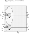
- Fig. 1a shows a sectional view of an embodiment of an enclosure.
- An intermediate layer 4 is arranged on top of the base layer 3, where the function zone 12 is arranged in an intermediate layer 4 of the enclosure 1.
- On top of the intermediate layer 4 a cover layer 5 is arranged. All of the layers 3,4,5 can also be multi-layered components, e.g. chemically hardened glass with an dielectric coating that covers one or both side partially or wholly. This can also be the case for all of the following descriptions.
- the function zone 12 is a cavity, where a function component 2 such as an electrical component or lens is situated inside the cavity 12.
- a respective contact surface 25 Between the base layer 3 and the intermediate layer 4 on the one side and the intermediate layer 4 and the cover layer 5 on the other side there is situated a respective contact surface 25.
- the base layer provides the bottom 22 of the cavity 12, the intermediate layer 4 comprises the side wall 21, where the cover layer 5 comprises the top 23 of the cavity 12.
- each interface zone 8 constitutes a circumferentially closed ring or closed line.
- Fig. 1c shows another example for an enclosure, where several intermediate layers 4a, 4b, 4c are used, and a stack 18 of layers 3, 4a, 4b, 4c, 5 is formed. Again, at each contact surface 25 there is arranged a respective laser weld line 8. As a result of the laser welding, the respective layer or substrate is firmly bonded or affixed to the neighbouring layer.
- the top layer 5 of this example might be a glass layer.
- the intermediate layers 4a, 4b and 4c may also be provided as a multilayer compound 4, and the cavity 12 can then be cleared e.g. by means of an abrasive method.
- the base substrate can be a wafer or a printed circuit board, for example made from aluminium nitride.
- the function zone 12 can also be formed as a recess e.g. in the base layer 3, made e.g. by an abrasive method such as sandblasting.
- Fig. 2 shows a top view of an enclosure 1 according to the invention, where the circumferential laser weld line 8 encloses the function zone 13.
- the function zone 13 can be designed to meet different requirements according to the needs, for example this can be an optical receptor, or a technical, electromechanical and/or device 2 arranged in the function zone 13. It is also possible, that several different tasks are accomplished by the function zone 13, e.g. in that different devices 2 are installed in a function zone 13.
- FIG. 3 another sectional view of an embodiment of the enclosure 1 comprising a base layer 3 and a cover layer 5, both in the form of substrates.
- the enclosure 1 comprises two layers, a base substrate 3 and a cover substrate 5.
- Fig. 3 indicates how a laser weld line 8 is typically composed, which is, that a multitude of laser pulses 16 is set so close to each other and aligned in the form of a line so that the material of the base substrate 3 and the cover layer 5 melts and merges with each other, preferably without any gap, so that as a result the function zone 13 or the cavity 12 is hermetically sealed by means of the laser weld line 8 or the laser weld lines 8 surrounding the function zone 13 or the cavity 12.
- FIG. 4 shows a cross-section of a typical weld line 8, which is, the cross-section of a modification caused by several laser pulse shots 16, where the many shots of laser pulses 16 cause through overlapping nonlinear absorption zones a line where heat accumulation takes place and a laser weld line 8 forms.
- the cross-section through such a weld line is depicted in Fig. 4 . It comprises several distinguishable areas.
- an elongated "bubble-shaped" region 32 (also referred to as "bubble 32" due to its typically quite characteristic shape comparable to an elongated bubble) can be formed which is only a few micrometre in width, but typically up to several tens of micrometre in height.
- a melting region 33 with a width w and an height h, where temperatures above Tg may be reached and the glass therefore (after cooling or dissipation of warmth) has resolidified.
- the melting region 33 with the included elongated bubble 32 can usually clearly be identified, e.g., with a light microscope, since its density and with this the refractive index has changed with respect to the surrounding glass. In some cases the area of nonlinear absorption 31 can also be observed as optical damage on the lower tip of the melting region 33.
- the glass Around the melting region 33 and in a heated region 34 the glass has received from heat accumulation of the multiple laser shot 9 an amount of energy by means of which its temperature raises to lower than Tg (the melting temperature of the respective material) but still significantly above room temperature. Due to heat diffusion this temperature is not the same in every corner of the heated region 34.
- Tg the melting temperature of the respective material
- the size of the heated region 34 scales with the size of the melting region 33. Thus, the dimensions and in particular the boundary of the melting region 33 can serve as an indicator for the dimensions of the heated region 34.
- any weld line 8 may also double serve as a local heat source for tempering the substrate material. Tempering is typically known as a heat treatment of glass in order to make it stronger, more resistant to heat and break. This is the same for the tempering presented in this disclosure, but however without the several disadvantages of any tempering method as known in the art.
- the heat region 34 may be placed by means of a weld line 8 and with respect to the to be tempered region or feature. By means of such a tempering feature, former weld lines 8 may be stress reduced, or even micro-cracks may be removed from the material.
- the material of the respective substrate layer has received an amount of stress which is stored therein.
- the stress introduced by the first laser weld line 8 can be reduced, and may even be cancelled out as will be explained further below.
- table 1 when improving an edge of a cavity 12, micro cracks can be eliminated, so that the cavity 12 is more stable and comprises a higher resistance with respect to any forces from outside or inside.
- cleaving tensions in a pre-scored plane cleaving tensions can be healed and at the same time also micro cracks reduced or eliminated.
- a gradient refractive index can be set up which may reduce losses of the waveguide.
- the lower laser weld line 8 has been performed first, and a "curing" second laser weld line 8a has been performed thereafter. Any distortion which had been introduced by the first laser weld line 8 has been neutralized by performing the second laser weld line 8a.
- the two laser weld lines 8, 8a achieve the additional feature that substrates are welded together, where the first laser weld line 8 welds the base substrate 3 to the first intermediate layer 4a, and the second laser weld line 8a welds the first intermediate layer 4a with the second intermediate layer 4b along each contacting area 25.
- the Figs. 6 to 14 show an exemplary way of composing an enclosure 1 according to the invention, which is also a method of manufacturing the same.
- the enclosure 1 of this embodiment is covered on both sides by means of a cover substrate which may be thinner than the "inner" substrates, but this is of exemplary reason only.
- Introducing additional cover substrates on both sides of the template may be advantageous as will be described below in more detail, as has been found out in making the present invention, that by introducing additional cover substrates it can be possible to eliminate even more stress in the materials of the inner substrates.
- a lower cover substrate 3 is provided and a first intermediate layer 4a is arranged on top of the lower cover substrate 3.
- an intermediate product 1 is formed, but in a simple embodiment an enclosure 1 could yet be formed by adjoining two layers and welding each enclosure 1 by at least one laser weld line 8.
- Fig. 8 shows the substrate stack 18 in the moment of placing a second and a third weld line 8a, 8b into the enclosure 1, where a second intermediate layer 4b is arranged on top of the first intermediate layer 4a.
- the second intermediate layer 4b constitutes the rim 21 or the "frame" of the future cavities 12.
- the stressed zones 35 are indicated similar to the embodiment of Fig. 7 as in the moment where the embodiment of Fig. 8 is shown the stressed zones 35 still persist, but will decrease thereafter as indicated in Fig. 9 .
- electronics or function components 2 can be installed in the enclosure 1, which would not be possible with normal tempering due to the necessary high temperatures throughout the whole material of the enclosure 1.
- the outermost layers which are the lower cover layer 3 and the upper cover layer 5, can for example be tempered (which is: relieved of stress) by means of classical methods, which is, by means of heating up the layers 3, 5 above a melting temperature.
- Fig. 14 an embodiment is shown, where a full stack 18 of substrates 3, 4a, 4b, 4c and 5 is arranged on each other, where the laser weld lines 8, 8a, 8b, 8c, 8d and 8e are introduced into the material one after another. Finally, the two enclosures 1 are cut or separated along the dicing line 10, and with Fig. 15 a single enclosure 1 is shown which can be obtained with the above explained method of manufacturing the same.
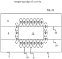
- FIG. 16 another example of tempering around the edge of a cavity 12 is shown.
- An at least two-dimensional weld line 8 is performed around the cavity 12, where by means of the laser weld line 8 not only the formerly separated substrates 3, 4 and 5 are welded together, but also any stress in the zone surrounding the cavity 12 is eliminated or at least significantly reduced, including elimination of possible micro cracks.
- Such micro cracks can be persistent in the material, or be brought in the material e.g. when cutting out material for making the cavity 12.
- a subsequent line of laser shots 16 is set close to each other to build the laser weld line 8 around the cavity 12.
- each enclosure 1 comprises three cavities 12, and at the same time where three enclosures 1 are made together in the same manufacturing process, but are separated in a separation step after finishing laser welding for example along the dicing lines 10 indicated in Fig. 17 .
- Several laser weld lines 8 are introduced into the material as described above in order to eliminate or decrease stress in the material of the enclosures 1.
- Each cavity 12 typically comprises a function component 2, whereas such a function component 2 is indicated in one cavity 12 only for reasons of ease of understanding.
- Fig. 18 shows a photography of two substrates 3 and 5 laser welded together along a laser weld line 8, where the change in refractive property can be seen as well as the reduction of stress in the material, which shall serve as proof-of-principle of the above-indicated method and enclosure 1.
Landscapes
- Engineering & Computer Science (AREA)
- Physics & Mathematics (AREA)
- Optics & Photonics (AREA)
- Mechanical Engineering (AREA)
- Plasma & Fusion (AREA)
- Chemical & Material Sciences (AREA)
- Microelectronics & Electronic Packaging (AREA)
- Materials Engineering (AREA)
- Organic Chemistry (AREA)
- Manufacturing & Machinery (AREA)
- Laser Beam Processing (AREA)
- Led Device Packages (AREA)
- Condensed Matter Physics & Semiconductors (AREA)
- General Physics & Mathematics (AREA)
- Computer Hardware Design (AREA)
- Power Engineering (AREA)
- Micromachines (AREA)
Claims (22)
- Umhäusung (1), umfassend:mindestens ein Basissubstrat (3) und ein Abdecksubstrat (5), die zumindest einen Teil der Umhäusung bilden, wobei die Umhäusung (1) entweder das Basissubstrat (3) und das Abdecksubstrat (5) als zwei Schichten umfasst oder wobei die Umhäusung ferner mindestens eine Zwischenschicht (4, 4a, 4b, 4c, 4d, 4e) umfasst, die zwischen der Basisschicht (3) und der Abdeckschicht (5) angeordnet ist,einen Funktionsbereich (12, 13), welcher derart angeordnet ist, dass er zumindest teilweise in der Umhäusung eingeschlossen ist,wobei zumindest das Abdecksubstrat ein Glas oder ein glasartiges Material oder ein Material auf Siliziumbasis umfasst und wobei vorzugsweise auch das Basissubstrat ein Glas oder ein glasartiges Material oder ein Material auf Siliziumbasis umfasst,wobei das Basissubstrat und das Abdecksubstrat mittels mindestens einer Laserbondlinie (8) verschweißt sind,wobei die Laserbondlinie eine Höhe HL in einer Richtung senkrecht zu ihrer Verbindungsebene aufweist,wobei die Umhäusung mindestens eine zweite Laserbondlinie (8a, 8b, 8c, 8d, 8e, 8f) umfasst, die neben der ersten Laserbondlinie angeordnet ist und/oder derart angeordnet ist, dass die mechanische Spannung in der mindestens einen Laserbondlinie mittels der zweiten Laserbondlinie reduziert wird, wodurch die mechanische Stabilität der Umhäusung verbessert ist.
- Umhäusung (1) gemäß dem vorhergehenden Anspruch,
wobei die mechanische Spannung in der mindestens einen Laserbondlinie (8) mittels eines Prozessschrittes zu Spannungsreduktion und/oder mittels eines Schrittes zur Rissreduktion reduziert wird. - Umhäusung (1) nach Anspruch 1 oder 2,wobei die erste Laserbondlinie (8) eine Spannungszone (35) in die Umhäusung einbringt,wobei die zweite Laserbondlinie (8a, 8b, 8c, 8d, 8e, 8f) in oder neben der durch die erste Laserbondlinie eingebrachten Spannungszone angeordnet ist undwobei die zweite Laserbondlinie die Spannungszone entlastet, so dass eine spannungsfreie oder nahezu spannungsfreie Zone entsteht und/oder so dass die laserverschweißte Umhäusung spannungsfrei oder nahezu spannungsfrei ist.
- Umhäusung (1) nach mindestens einem der vorhergehenden Ansprüche, ferner mit einem Hohlraum (12) im Inneren der Umhäusung, wobei der Funktionsbereich (13) diesen Hohlraum darstellt, ferner umfassend eine mindestens zweidimensionale Laserbondlinie (8) um den Hohlraum herum zum Tempern der Kanten des Hohlraums.
- Umhäusung (1) nach mindestens einem der vorhergehenden Ansprüche, wobei die mindestens eine Laserbondlinie (8, 8a, 8b, 8c, 8d, 8e, 8f) den Funktionsbereich (12, 13) in einem Abstand DF umläuft, wobei der Abstand beispielsweise der Höhe HF oder weniger entspricht, oder der doppelten Höhe HF oder weniger entspricht.
- Umhäusung (1) nach mindestens einem der vorhergehenden Ansprüche,wobei die Umhäusung eine hermetische Abdichtung für den Funktionsbereich bietet, so dass es sich bei der Umhäusung um eine hermetisch abgedichtete Umhäusung handelt, und/oderwobei der Funktionsbereich (13) umlaufend von der Umhäusung eingeschlossen ist.
- Umhäusung (1) nach mindestens einem der vorhergehenden Ansprüche,
ferner mit einer elastischen oder flexiblen Schicht (4a, 4b, 4c, 4d), so dass die Umhäusung verformbar ist, beispielsweise durch Druckänderung oder durch mechanische Kraft. - Umhäusung (1) nach mindestens einem der vorhergehenden Ansprüche, ferner mit einem innerem Beschichtungsbereich (36), der beispielsweise um den Funktionsbereich (12, 13) herum angeordnet ist.
- Umhäusung (1) nach mindestens einem der vorhergehenden Ansprüche, wobei mindestens eines der Substrate der Umhäusung als Mehrschichtverbund (4) ausgebildet ist, beispielsweise mit einer oder mehreren Beschichtungslagen oder Vorspannungszonen und/oder einem oder mehreren Substraten.
- Umhäusung (1) nach mindestens einem der vorhergehenden Ansprüche, wobei die Zwischenschicht als Mehrschichtverbund ausgebildet ist.
- Umhäusung (1) nach mindestens einem der vorhergehenden Ansprüche, wobei sich der Funktionsbereich (12, 13) in der oder einer der Zwischenschichten (4, 4a, 4b, 4c, 4d, 4e) befindet und an seiner Unterseite durch die Basisschicht (3) und an seiner Oberseite durch die Abdeckschicht (5) abgedeckt ist.
- Umhäusung (1) nach mindestens einem der vorhergehenden Ansprüche, wobei der Funktionsbereich (12, 13) ein Hohlraum (12) ist und wobei eine Funktionskomponente (2) wie beispielsweise ein elektrisches Bauelement in dem Hohlraum angeordnet ist, um durch die Umhäusung geschützt zu sein.
- Umhäusung (1) gemäß dem vorhergehenden Anspruch, wobei die Funktionskomponente (2) einen im Inneren des Hohlraums (12) angeordneten Leistungshalbleiter umfasst, beispielsweise eine GaN-LED, einen SiC-, GaAs- oder GaN-Leistungstransistor.
- Umhäusung (1) nach mindestens einem der vorhergehenden Ansprüche, wobei die Laserbondlinie (8, 8a, 8b, 8c, 8d, 8e, 8f) jeweils derart angeordnet ist, dass sie sich in zwei unterschiedliche Substrate (3, 4a, 4b, 4c, 4d, 4e, 4f, 5) der Umhäusung hinein erstreckt, wobei sich die Laserbondlinie beispielsweise von der Basisabdeckschicht (3) in die obere Abdeckschicht (5) hinein erstreckt und wobei die Laserbondlinie die beiden unterschiedlichen Substrate miteinander verschweißt.
- Umhäusung (1) nach mindestens einem der vorhergehenden Ansprüche,wobei die Substrate (3, 4a, 4b, 4c, 4d, 4e, 4f, 5) eine Dicke von weniger als 3 mm aufweisen, vorzugsweise von weniger als 1500 µm, vorzugsweise von weniger als 500 µm, vorzugsweise von weniger als 120 µm und weiter bevorzugt von weniger als 80 µm, und/oderwobei die Basisabdeckschicht (3) und/oder die obere Abdeckschicht (5) dünner ist/sind als die eine oder die mehreren Zwischenschichten (4a, 4b, 4c, 4d, 4e, 4f), beispielsweise halb so dick wie die Zwischenschichten oder dünner.
- Umhäusung (1) nach mindestens einem der vorhergehenden Ansprüche, wobei mindestens eine der Substratlagen (3, 4a, 4b, 4c, 4d, 4e, 4f, 5), beispielsweise die Basisabdeckschicht (3), Durchkontaktierungen zur elektrischen Kontaktierung des Funktionsbereichs (12, 13) mit der umgebenden Außenseite der Umhäusung, beispielsweise einem Kontaktpad auf der Unterseite der Basisabdeckschicht, umfasst.
- Umhäusung (1) nach mindestens einem der vorhergehenden Ansprüche,wobei die Umhäusung eine Größe von 10 mm x 10 mm oder weniger, vorzugsweise 5 mm x 5 mm oder weniger, weiter bevorzugt von 2 mm x 2 mm oder 1 mm x 1 mm oder weniger aufweist, und/oderwobei die Umhäusung eine Höhe aufweist, die größer ist als ihre Breite.
- Verwendung einer Umhäusung (1) nach mindestens einem der vorhergehenden Ansprüche zur Herstellung eines medizinischen Implantats, eines Mikrolinsenverbunds, eines mikrooptischen Chips, einer pharmazeutischen Verpackung, einer LED oder einer optischen Baugruppe für ein Augmented-Reality-Gerät.
- Verfahren zum Bereitstellen einer Umhäusung (1) nach einem der vorhergehenden Ansprüche, wobei die Umhäusung einen Funktionsbereich (12, 13) wie etwa einen Hohlraum (12) umschließt, wobei das Verfahren die folgenden Schritte umfasst:Bereitstellen eines Basissubstrats (3) und Ausrichten eines Abdecksubstrats (5) über dem Basissubstrat in solcher Weise, dass sich zwischen dem Basissubstrat und dem Abdecksubstrat zumindest eine Kontaktfläche (25) befindet,hermetisches Abdichten des Funktionsbereichs durch Einbringen einer ersten Laserbondlinie (8) in die Umhäusung,Einbringen einer zweiten Laserbondlinie (8a, 8b, 8c, 8d, 8e, 8f) an der gleichen Stelle wie die erste Laserbondlinie oder an einer Stelle nahe der ersten Laserbondlinie oder mit dieser überlappend, und Entlasten der Spannung in dem Bereich der ersten Laserbondlinie der Umhäusung durch Einbringen der zweiten Laserbondlinie,wobei zumindest das Abdecksubstrat ein Glas oder ein glasartiges Material oder ein Material auf Siliziumbasis umfasst und wobei vorzugsweise auch das Basissubstrat ein Glas oder ein glasartiges Material oder ein Material auf Siliziumbasis umfasst.
- Verfahren zum Bereitstellen einer Umhäusung (1) gemäß dem vorhergehenden Anspruch,wobei eine Laserstrahlquelle (9) verwendet wird, um die Laserbondlinien (8, 8a, 8b, 8c, 8d, 8e, 8f) in die Umhäusung einzubringen, undwobei der Laserstrahl um den Funktionsbereich (12, 13) herum geführt wird, um die Laserbondlinie entlang der Kontaktfläche (25) zwischen dem Basissubstrat (3) und dem Abdecksubstrat (5) zu erzeugen.
- Verfahren gemäß dem vorhergehenden Anspruch, wobei die Laserquelle (9) eine gepulste Laserquelle ist und wobei mehrere Laserimpulse entlang der Laserbondlinie (8, 8a, 8b, 8c, 8d, 8e, 8f) eingebracht werden, so dass aus den mehreren Laserimpulsen eine durchgehende oder nahezu durchgehende Bondlinie zusammengesetzt wird.
- Getemperte abgedichtete Umhäusung (1), hergestellt mit dem Verfahren gemäß einem der vorhergehenden Verfahrensansprüche.
Priority Applications (8)
| Application Number | Priority Date | Filing Date | Title |
|---|---|---|---|
| EP19205115.9A EP3812352B1 (de) | 2019-10-24 | 2019-10-24 | Glasverbundanordnung |
| FIEP19205115.9T FI3812352T3 (fi) | 2019-10-24 | 2019-10-24 | Lasiyhdistejärjestely |
| PCT/EP2020/079486 WO2021078731A1 (en) | 2019-10-24 | 2020-10-20 | Glass compound arrangement |
| EP20792431.7A EP4048643A1 (de) | 2019-10-24 | 2020-10-20 | Glasverbundanordnung |
| JP2022518364A JP7717055B2 (ja) | 2019-10-24 | 2020-10-20 | ガラス複合体装置 |
| AU2020371187A AU2020371187B2 (en) | 2019-10-24 | 2020-10-20 | Glass compound arrangement |
| CN202080073902.1A CN114599474B (zh) | 2019-10-24 | 2020-10-20 | 玻璃复合布置 |
| US17/726,937 US20220241897A1 (en) | 2019-10-24 | 2022-04-22 | Glass compound arrangement |
Applications Claiming Priority (1)
| Application Number | Priority Date | Filing Date | Title |
|---|---|---|---|
| EP19205115.9A EP3812352B1 (de) | 2019-10-24 | 2019-10-24 | Glasverbundanordnung |
Publications (2)
| Publication Number | Publication Date |
|---|---|
| EP3812352A1 EP3812352A1 (de) | 2021-04-28 |
| EP3812352B1 true EP3812352B1 (de) | 2025-06-04 |
Family
ID=68342811
Family Applications (2)
| Application Number | Title | Priority Date | Filing Date |
|---|---|---|---|
| EP19205115.9A Active EP3812352B1 (de) | 2019-10-24 | 2019-10-24 | Glasverbundanordnung |
| EP20792431.7A Pending EP4048643A1 (de) | 2019-10-24 | 2020-10-20 | Glasverbundanordnung |
Family Applications After (1)
| Application Number | Title | Priority Date | Filing Date |
|---|---|---|---|
| EP20792431.7A Pending EP4048643A1 (de) | 2019-10-24 | 2020-10-20 | Glasverbundanordnung |
Country Status (7)
| Country | Link |
|---|---|
| US (1) | US20220241897A1 (de) |
| EP (2) | EP3812352B1 (de) |
| JP (1) | JP7717055B2 (de) |
| CN (1) | CN114599474B (de) |
| AU (1) | AU2020371187B2 (de) |
| FI (1) | FI3812352T3 (de) |
| WO (1) | WO2021078731A1 (de) |
Families Citing this family (8)
| Publication number | Priority date | Publication date | Assignee | Title |
|---|---|---|---|---|
| CN114373847A (zh) * | 2021-12-31 | 2022-04-19 | 泉州三安半导体科技有限公司 | Led封装器件 |
| DE102022116612B4 (de) | 2022-07-04 | 2025-10-23 | Schott Ag | Hermetisch verschlossene Umhäusung und Verfahren zur Auslegung der Schweißverbindung für eine solche Umhäusung |
| EP4393869A1 (de) * | 2022-12-28 | 2024-07-03 | Schott Ag | Verfahren zum schweissen von substraten und geschweisste substrate |
| EP4424651A1 (de) | 2023-03-02 | 2024-09-04 | Schott Ag | Gebondete substratanordnung und verfahren zur herstellung solch einer anordnung |
| EP4487903B1 (de) | 2023-07-07 | 2025-06-04 | Schott Ag | Hermetische umfassung mit glasdurchgängen und medizinisches implantat mit einer solchen hermetischen umfassung |
| SE547705C2 (en) * | 2024-02-15 | 2025-11-11 | Gapwaves Ab | Method for manufacturing thin multi-layer waveguide assembly and a thin multi-layer waveguide assembly |
| DE102024113263A1 (de) * | 2024-05-13 | 2025-11-13 | Schott Ag | Verbundene Anordnung und Verfahren zur Herstellung einer verbundenen Anordnung |
| EP4678222A1 (de) | 2024-07-08 | 2026-01-14 | Schott Ag | Implantierbare vorrichtung |
Citations (1)
| Publication number | Priority date | Publication date | Assignee | Title |
|---|---|---|---|---|
| WO2018211176A1 (en) * | 2017-05-19 | 2018-11-22 | Primoceler Oy | Method and apparatus for producing a hermetic vacuum joint at low temperature |
Family Cites Families (12)
| Publication number | Priority date | Publication date | Assignee | Title |
|---|---|---|---|---|
| JP2000313630A (ja) * | 1998-08-07 | 2000-11-14 | Shin Meiwa Ind Co Ltd | ガラス融着方法、ガラス融着装置、融着ガラスおよび融着ガラスの製造方法 |
| EP2075082B1 (de) * | 2006-09-22 | 2015-11-11 | NEC SCHOTT Components Corporation | Materialverbindungsverfahren |
| DE102010038554A1 (de) | 2010-07-28 | 2012-02-02 | Osram Ag | Optoelektronisches Halbleiterbauelement und zugehöriges Herstellverfahren |
| CN102403466B (zh) * | 2011-11-18 | 2014-12-31 | 上海大学 | 一种用于光电器件封装的激光键合方法 |
| CN103367658B (zh) | 2013-07-17 | 2016-08-31 | 深圳市华星光电技术有限公司 | 一种玻璃封装结构和封装方法 |
| JP2015188939A (ja) * | 2014-03-31 | 2015-11-02 | アイシン精機株式会社 | レーザ接合方法、レーザ接合品及びレーザ接合装置 |
| KR20160147833A (ko) * | 2014-04-21 | 2016-12-23 | 코닝 인코포레이티드 | 고 열팽창 유리 및 유리-세라믹의 레이저 용접 |
| WO2016032885A1 (en) | 2014-08-25 | 2016-03-03 | Corning Incorporated | Sealed device and methods for making the same |
| FI125935B (fi) | 2014-09-26 | 2016-04-15 | Primoceler Oy | Menetelmä optisen komponentin suojana käytettävän läpinäkyvän kappaleen valmistamiseksi |
| JP2017204599A (ja) | 2016-05-13 | 2017-11-16 | 日本電気硝子株式会社 | 気密パッケージの製造方法及び気密パッケージ |
| CN106735895B (zh) * | 2016-12-15 | 2018-09-11 | 苏州大学 | 一种铝合金-玻璃复合材料的激光焊接方法 |
| KR102755456B1 (ko) | 2019-01-04 | 2025-01-20 | 삼성디스플레이 주식회사 | 표시 장치 및 이의 제조 방법 |
-
2019
- 2019-10-24 EP EP19205115.9A patent/EP3812352B1/de active Active
- 2019-10-24 FI FIEP19205115.9T patent/FI3812352T3/fi active
-
2020
- 2020-10-20 CN CN202080073902.1A patent/CN114599474B/zh active Active
- 2020-10-20 AU AU2020371187A patent/AU2020371187B2/en active Active
- 2020-10-20 JP JP2022518364A patent/JP7717055B2/ja active Active
- 2020-10-20 WO PCT/EP2020/079486 patent/WO2021078731A1/en not_active Ceased
- 2020-10-20 EP EP20792431.7A patent/EP4048643A1/de active Pending
-
2022
- 2022-04-22 US US17/726,937 patent/US20220241897A1/en active Pending
Patent Citations (1)
| Publication number | Priority date | Publication date | Assignee | Title |
|---|---|---|---|---|
| WO2018211176A1 (en) * | 2017-05-19 | 2018-11-22 | Primoceler Oy | Method and apparatus for producing a hermetic vacuum joint at low temperature |
Also Published As
| Publication number | Publication date |
|---|---|
| WO2021078731A1 (en) | 2021-04-29 |
| EP4048643A1 (de) | 2022-08-31 |
| AU2020371187B2 (en) | 2023-05-04 |
| CN114599474A (zh) | 2022-06-07 |
| US20220241897A1 (en) | 2022-08-04 |
| FI3812352T3 (fi) | 2025-08-21 |
| CN114599474B (zh) | 2025-03-11 |
| JP7717055B2 (ja) | 2025-08-01 |
| EP3812352A1 (de) | 2021-04-28 |
| JP2022554060A (ja) | 2022-12-28 |
| AU2020371187A1 (en) | 2022-04-07 |
Similar Documents
| Publication | Publication Date | Title |
|---|---|---|
| EP3812352B1 (de) | Glasverbundanordnung | |
| EP3861389B1 (de) | Schweissschutz für hermetische abdichtung auf wafer-ebene | |
| WO2009108335A2 (en) | Hermetically-sealed packages for electronic components having reduced unused areas | |
| JP7664910B2 (ja) | 密閉されたガラス筐体 | |
| JP2024546037A (ja) | 気密接続アセンブリ | |
| US11993511B2 (en) | Hermetically sealed, toughened glass package and method for producing same | |
| CN109003971B (zh) | 用于光电器件的外壳及其生产方法、以及用于外壳的盖 | |
| CN115996888A (zh) | 气密性密封的封装件及其生产方法 | |
| US20240417244A1 (en) | Enclosure | |
| CN114206771A (zh) | 严密密封的玻璃封装件 | |
| US11975962B2 (en) | Hermetically sealed transparent cavity and package for same | |
| CN114945534A (zh) | 气密封闭的透明的凹腔及其封壳 | |
| EP4424651A1 (de) | Gebondete substratanordnung und verfahren zur herstellung solch einer anordnung | |
| US20260014647A1 (en) | Hermetically sealed enclosure and method for designing the weld connection for such an enclosure |
Legal Events
| Date | Code | Title | Description |
|---|---|---|---|
| STAA | Information on the status of an ep patent application or granted ep patent |
Free format text: STATUS: EXAMINATION IS IN PROGRESS |
|
| PUAI | Public reference made under article 153(3) epc to a published international application that has entered the european phase |
Free format text: ORIGINAL CODE: 0009012 |
|
| 17P | Request for examination filed |
Effective date: 20191024 |
|
| AK | Designated contracting states |
Kind code of ref document: A1 Designated state(s): AL AT BE BG CH CY CZ DE DK EE ES FI FR GB GR HR HU IE IS IT LI LT LU LV MC MK MT NL NO PL PT RO RS SE SI SK SM TR |
|
| AX | Request for extension of the european patent |
Extension state: BA ME |
|
| P01 | Opt-out of the competence of the unified patent court (upc) registered |
Effective date: 20230516 |
|
| REG | Reference to a national code |
Ref country code: DE Free format text: PREVIOUS MAIN CLASS: C03B0023240000 Ref country code: DE Ref legal event code: R079 Ref document number: 602019070695 Country of ref document: DE Free format text: PREVIOUS MAIN CLASS: C03B0023240000 Ipc: B23K0026062200 |
|
| RIC1 | Information provided on ipc code assigned before grant |
Ipc: B81C 1/00 20060101ALI20241219BHEP Ipc: B23K 103/00 20060101ALI20241219BHEP Ipc: B23K 101/36 20060101ALI20241219BHEP Ipc: B23K 101/18 20060101ALI20241219BHEP Ipc: B23K 26/22 20060101ALI20241219BHEP Ipc: B23K 26/324 20140101ALI20241219BHEP Ipc: B23K 26/244 20140101ALI20241219BHEP Ipc: B23K 26/20 20140101ALI20241219BHEP Ipc: C03B 23/24 20060101ALI20241219BHEP Ipc: B23K 26/0622 20140101AFI20241219BHEP |
|
| GRAP | Despatch of communication of intention to grant a patent |
Free format text: ORIGINAL CODE: EPIDOSNIGR1 |
|
| STAA | Information on the status of an ep patent application or granted ep patent |
Free format text: STATUS: GRANT OF PATENT IS INTENDED |
|
| INTG | Intention to grant announced |
Effective date: 20250130 |
|
| GRAS | Grant fee paid |
Free format text: ORIGINAL CODE: EPIDOSNIGR3 |
|
| GRAA | (expected) grant |
Free format text: ORIGINAL CODE: 0009210 |
|
| STAA | Information on the status of an ep patent application or granted ep patent |
Free format text: STATUS: THE PATENT HAS BEEN GRANTED |
|
| AK | Designated contracting states |
Kind code of ref document: B1 Designated state(s): AL AT BE BG CH CY CZ DE DK EE ES FI FR GB GR HR HU IE IS IT LI LT LU LV MC MK MT NL NO PL PT RO RS SE SI SK SM TR |
|
| REG | Reference to a national code |
Ref country code: GB Ref legal event code: FG4D |
|
| REG | Reference to a national code |
Ref country code: CH Ref legal event code: EP |
|
| REG | Reference to a national code |
Ref country code: DE Ref legal event code: R096 Ref document number: 602019070695 Country of ref document: DE |
|
| REG | Reference to a national code |
Ref country code: IE Ref legal event code: FG4D |
|
| REG | Reference to a national code |
Ref country code: FI Ref legal event code: FGE |
|
| REG | Reference to a national code |
Ref country code: NL Ref legal event code: MP Effective date: 20250604 |
|
| PG25 | Lapsed in a contracting state [announced via postgrant information from national office to epo] |
Ref country code: ES Free format text: LAPSE BECAUSE OF FAILURE TO SUBMIT A TRANSLATION OF THE DESCRIPTION OR TO PAY THE FEE WITHIN THE PRESCRIBED TIME-LIMIT Effective date: 20250604 |
|
| REG | Reference to a national code |
Ref country code: LT Ref legal event code: MG9D |
|
| PG25 | Lapsed in a contracting state [announced via postgrant information from national office to epo] |
Ref country code: NO Free format text: LAPSE BECAUSE OF FAILURE TO SUBMIT A TRANSLATION OF THE DESCRIPTION OR TO PAY THE FEE WITHIN THE PRESCRIBED TIME-LIMIT Effective date: 20250904 Ref country code: GR Free format text: LAPSE BECAUSE OF FAILURE TO SUBMIT A TRANSLATION OF THE DESCRIPTION OR TO PAY THE FEE WITHIN THE PRESCRIBED TIME-LIMIT Effective date: 20250905 |
|
| PG25 | Lapsed in a contracting state [announced via postgrant information from national office to epo] |
Ref country code: PL Free format text: LAPSE BECAUSE OF FAILURE TO SUBMIT A TRANSLATION OF THE DESCRIPTION OR TO PAY THE FEE WITHIN THE PRESCRIBED TIME-LIMIT Effective date: 20250604 |
|
| PG25 | Lapsed in a contracting state [announced via postgrant information from national office to epo] |
Ref country code: BG Free format text: LAPSE BECAUSE OF FAILURE TO SUBMIT A TRANSLATION OF THE DESCRIPTION OR TO PAY THE FEE WITHIN THE PRESCRIBED TIME-LIMIT Effective date: 20250604 |
|
| PG25 | Lapsed in a contracting state [announced via postgrant information from national office to epo] |
Ref country code: HR Free format text: LAPSE BECAUSE OF FAILURE TO SUBMIT A TRANSLATION OF THE DESCRIPTION OR TO PAY THE FEE WITHIN THE PRESCRIBED TIME-LIMIT Effective date: 20250604 |
|
| PG25 | Lapsed in a contracting state [announced via postgrant information from national office to epo] |
Ref country code: RS Free format text: LAPSE BECAUSE OF FAILURE TO SUBMIT A TRANSLATION OF THE DESCRIPTION OR TO PAY THE FEE WITHIN THE PRESCRIBED TIME-LIMIT Effective date: 20250904 |
|
| PG25 | Lapsed in a contracting state [announced via postgrant information from national office to epo] |
Ref country code: LV Free format text: LAPSE BECAUSE OF FAILURE TO SUBMIT A TRANSLATION OF THE DESCRIPTION OR TO PAY THE FEE WITHIN THE PRESCRIBED TIME-LIMIT Effective date: 20250604 |
|
| REG | Reference to a national code |
Ref country code: CH Ref legal event code: U11 Free format text: ST27 STATUS EVENT CODE: U-0-0-U10-U11 (AS PROVIDED BY THE NATIONAL OFFICE) Effective date: 20251101 |
|
| PG25 | Lapsed in a contracting state [announced via postgrant information from national office to epo] |
Ref country code: NL Free format text: LAPSE BECAUSE OF FAILURE TO SUBMIT A TRANSLATION OF THE DESCRIPTION OR TO PAY THE FEE WITHIN THE PRESCRIBED TIME-LIMIT Effective date: 20250604 |
|
| PG25 | Lapsed in a contracting state [announced via postgrant information from national office to epo] |
Ref country code: PT Free format text: LAPSE BECAUSE OF FAILURE TO SUBMIT A TRANSLATION OF THE DESCRIPTION OR TO PAY THE FEE WITHIN THE PRESCRIBED TIME-LIMIT Effective date: 20251006 |
|
| REG | Reference to a national code |
Ref country code: AT Ref legal event code: MK05 Ref document number: 1799910 Country of ref document: AT Kind code of ref document: T Effective date: 20250604 |
|
| PG25 | Lapsed in a contracting state [announced via postgrant information from national office to epo] |
Ref country code: IS Free format text: LAPSE BECAUSE OF FAILURE TO SUBMIT A TRANSLATION OF THE DESCRIPTION OR TO PAY THE FEE WITHIN THE PRESCRIBED TIME-LIMIT Effective date: 20251004 |
|
| PGFP | Annual fee paid to national office [announced via postgrant information from national office to epo] |
Ref country code: DE Payment date: 20251021 Year of fee payment: 7 |
|
| PGFP | Annual fee paid to national office [announced via postgrant information from national office to epo] |
Ref country code: GB Payment date: 20251022 Year of fee payment: 7 |
|
| PG25 | Lapsed in a contracting state [announced via postgrant information from national office to epo] |
Ref country code: AT Free format text: LAPSE BECAUSE OF FAILURE TO SUBMIT A TRANSLATION OF THE DESCRIPTION OR TO PAY THE FEE WITHIN THE PRESCRIBED TIME-LIMIT Effective date: 20250604 Ref country code: SM Free format text: LAPSE BECAUSE OF FAILURE TO SUBMIT A TRANSLATION OF THE DESCRIPTION OR TO PAY THE FEE WITHIN THE PRESCRIBED TIME-LIMIT Effective date: 20250604 |
|
| PGFP | Annual fee paid to national office [announced via postgrant information from national office to epo] |
Ref country code: FI Payment date: 20251028 Year of fee payment: 7 |
|
| PGFP | Annual fee paid to national office [announced via postgrant information from national office to epo] |
Ref country code: FR Payment date: 20251030 Year of fee payment: 7 |
|
| PGFP | Annual fee paid to national office [announced via postgrant information from national office to epo] |
Ref country code: CH Payment date: 20251101 Year of fee payment: 7 |
|
| PG25 | Lapsed in a contracting state [announced via postgrant information from national office to epo] |
Ref country code: CZ Free format text: LAPSE BECAUSE OF FAILURE TO SUBMIT A TRANSLATION OF THE DESCRIPTION OR TO PAY THE FEE WITHIN THE PRESCRIBED TIME-LIMIT Effective date: 20250604 |
|
| PG25 | Lapsed in a contracting state [announced via postgrant information from national office to epo] |
Ref country code: EE Free format text: LAPSE BECAUSE OF FAILURE TO SUBMIT A TRANSLATION OF THE DESCRIPTION OR TO PAY THE FEE WITHIN THE PRESCRIBED TIME-LIMIT Effective date: 20250604 |
|
| PG25 | Lapsed in a contracting state [announced via postgrant information from national office to epo] |
Ref country code: SK Free format text: LAPSE BECAUSE OF FAILURE TO SUBMIT A TRANSLATION OF THE DESCRIPTION OR TO PAY THE FEE WITHIN THE PRESCRIBED TIME-LIMIT Effective date: 20250604 Ref country code: RO Free format text: LAPSE BECAUSE OF FAILURE TO SUBMIT A TRANSLATION OF THE DESCRIPTION OR TO PAY THE FEE WITHIN THE PRESCRIBED TIME-LIMIT Effective date: 20250604 |
|
| PG25 | Lapsed in a contracting state [announced via postgrant information from national office to epo] |
Ref country code: IT Free format text: LAPSE BECAUSE OF FAILURE TO SUBMIT A TRANSLATION OF THE DESCRIPTION OR TO PAY THE FEE WITHIN THE PRESCRIBED TIME-LIMIT Effective date: 20250604 |