EP3811400B1 - System and method for self-cleaning wet treatment process - Google Patents
System and method for self-cleaning wet treatment process Download PDFInfo
- Publication number
- EP3811400B1 EP3811400B1 EP19822301.8A EP19822301A EP3811400B1 EP 3811400 B1 EP3811400 B1 EP 3811400B1 EP 19822301 A EP19822301 A EP 19822301A EP 3811400 B1 EP3811400 B1 EP 3811400B1
- Authority
- EP
- European Patent Office
- Prior art keywords
- spray
- wafer
- station
- sprayer
- cleaning
- Prior art date
- Legal status (The legal status is an assumption and is not a legal conclusion. Google has not performed a legal analysis and makes no representation as to the accuracy of the status listed.)
- Active
Links
Images










Classifications
-
- H—ELECTRICITY
- H10—SEMICONDUCTOR DEVICES; ELECTRIC SOLID-STATE DEVICES NOT OTHERWISE PROVIDED FOR
- H10P—GENERIC PROCESSES OR APPARATUS FOR THE MANUFACTURE OR TREATMENT OF DEVICES COVERED BY CLASS H10
- H10P72/00—Handling or holding of wafers, substrates or devices during manufacture or treatment thereof
- H10P72/04—Apparatus for manufacture or treatment
- H10P72/0402—Apparatus for fluid treatment
- H10P72/0406—Apparatus for fluid treatment for cleaning followed by drying, rinsing, stripping, blasting or the like
- H10P72/0411—Apparatus for fluid treatment for cleaning followed by drying, rinsing, stripping, blasting or the like for wet cleaning or washing
- H10P72/0416—Apparatus for fluid treatment for cleaning followed by drying, rinsing, stripping, blasting or the like for wet cleaning or washing with the semiconductor substrates being dipped in baths or vessels
-
- B—PERFORMING OPERATIONS; TRANSPORTING
- B08—CLEANING
- B08B—CLEANING IN GENERAL; PREVENTION OF FOULING IN GENERAL
- B08B3/00—Cleaning by methods involving the use or presence of liquid or steam
- B08B3/02—Cleaning by the force of jets or sprays
- B08B3/024—Cleaning by means of spray elements moving over the surface to be cleaned
-
- B—PERFORMING OPERATIONS; TRANSPORTING
- B08—CLEANING
- B08B—CLEANING IN GENERAL; PREVENTION OF FOULING IN GENERAL
- B08B3/00—Cleaning by methods involving the use or presence of liquid or steam
- B08B3/04—Cleaning involving contact with liquid
-
- B—PERFORMING OPERATIONS; TRANSPORTING
- B08—CLEANING
- B08B—CLEANING IN GENERAL; PREVENTION OF FOULING IN GENERAL
- B08B3/00—Cleaning by methods involving the use or presence of liquid or steam
- B08B3/04—Cleaning involving contact with liquid
- B08B3/10—Cleaning involving contact with liquid with additional treatment of the liquid or of the object being cleaned, e.g. by heat, by electricity or by vibration
-
- B—PERFORMING OPERATIONS; TRANSPORTING
- B08—CLEANING
- B08B—CLEANING IN GENERAL; PREVENTION OF FOULING IN GENERAL
- B08B9/00—Cleaning hollow articles by methods or apparatus specially adapted thereto
- B08B9/08—Cleaning containers, e.g. tanks
- B08B9/093—Cleaning containers, e.g. tanks by the force of jets or sprays
-
- H—ELECTRICITY
- H10—SEMICONDUCTOR DEVICES; ELECTRIC SOLID-STATE DEVICES NOT OTHERWISE PROVIDED FOR
- H10P—GENERIC PROCESSES OR APPARATUS FOR THE MANUFACTURE OR TREATMENT OF DEVICES COVERED BY CLASS H10
- H10P70/00—Cleaning of wafers, substrates or parts of devices
- H10P70/20—Cleaning during device manufacture
- H10P70/23—Cleaning during device manufacture during, before or after processing of insulating materials
-
- H—ELECTRICITY
- H10—SEMICONDUCTOR DEVICES; ELECTRIC SOLID-STATE DEVICES NOT OTHERWISE PROVIDED FOR
- H10P—GENERIC PROCESSES OR APPARATUS FOR THE MANUFACTURE OR TREATMENT OF DEVICES COVERED BY CLASS H10
- H10P72/00—Handling or holding of wafers, substrates or devices during manufacture or treatment thereof
- H10P72/04—Apparatus for manufacture or treatment
- H10P72/0402—Apparatus for fluid treatment
-
- H—ELECTRICITY
- H10—SEMICONDUCTOR DEVICES; ELECTRIC SOLID-STATE DEVICES NOT OTHERWISE PROVIDED FOR
- H10P—GENERIC PROCESSES OR APPARATUS FOR THE MANUFACTURE OR TREATMENT OF DEVICES COVERED BY CLASS H10
- H10P72/00—Handling or holding of wafers, substrates or devices during manufacture or treatment thereof
- H10P72/04—Apparatus for manufacture or treatment
- H10P72/0402—Apparatus for fluid treatment
- H10P72/0406—Apparatus for fluid treatment for cleaning followed by drying, rinsing, stripping, blasting or the like
- H10P72/0411—Apparatus for fluid treatment for cleaning followed by drying, rinsing, stripping, blasting or the like for wet cleaning or washing
- H10P72/0414—Apparatus for fluid treatment for cleaning followed by drying, rinsing, stripping, blasting or the like for wet cleaning or washing using mainly spraying means, e.g. nozzles
-
- H—ELECTRICITY
- H10—SEMICONDUCTOR DEVICES; ELECTRIC SOLID-STATE DEVICES NOT OTHERWISE PROVIDED FOR
- H10P—GENERIC PROCESSES OR APPARATUS FOR THE MANUFACTURE OR TREATMENT OF DEVICES COVERED BY CLASS H10
- H10P72/00—Handling or holding of wafers, substrates or devices during manufacture or treatment thereof
- H10P72/04—Apparatus for manufacture or treatment
- H10P72/0451—Apparatus for manufacturing or treating in a plurality of work-stations
- H10P72/0462—Apparatus for manufacturing or treating in a plurality of work-stations characterised by the construction of the processing chambers, e.g. modular processing chambers
Definitions
- the present invention relates to semiconductor fabrication equipment and processing, and in particular, relates to a system and method for removing residues from processing equipment used in a wet treatment process, including solvent immersion and film lift-off stations.
- Semiconductor fabrication typically involves deposition of a mask or pattern which determines the components and the electrical connections on a substrate.
- One common masking technique involves depositing photoresist across a substrate surface and then selectively exposing a pattern on the photoresist. During wet treatment, the pattern is etched onto the substrate material by removal of the exposed sections (or alternatively by sections that were not exposed, depending on the type of photoresist).
- By chemical development both exposed photoresist and material underlying the exposed photoresist can then be chemically removed by immersion in a solvent, resulting in a patterned structure.
- photoresist can be deposited first, underneath subsequently deposited material that is harder to dissolve. When solvent is applied, the photoresist dissolves and layers overlying the photoresist can be removed, or lifted-off, as well. During both the immersion phase and subsequent lift-off phase, a considerable amount of debris and residue can accumulate. Additionally, during immersion incompletely dissolved materials build-up in the solvent bath and can also remain on the meniscus on the wafer surface.
- GaAs Gallium Arsenide
- the wafer After immersion, the wafer is typically transferred to a spin chamber in which a high-pressure spray is applied to remove excess material and residual photoresist from the wafer.
- the residual debris tends to accumulate rapidly on walls of the spin chamber or in filters positioned in the fluid drain path, necessitating frequent cleaning of the spin chamber (e.g., several times per day).
- the time that the chambers spend offline reduces wafer throughput and the overall efficiency of the fabrication process.
- the high-pressure spray can damage the wafer surface as any adhering or trapped debris is dragged along by surface by the force of the spray.
- US 2004/074600 A1 that relates to a wet etch system with overflow particle removing feature, discloses a wet etch system including a process tank having an inner etch bath chamber and an outer overflow chamber surrounding the etch bath chamber.
- a frame which is removably mounted on the process tank defines a diversion channel between the upper ends of the etch bath chamber and overflow chamber.
- the etch bath chamber receives a wafer-containing cassette, which displaces etchant from the etch bath chamber, through the diversion channel and into the overflow chamber, where the etchant is drained from the process tank.
- Particulate impurities leave the etch bath chamber, enter the overflow chamber and drain from the process tank with the overflow etchant.
- Fresh etchant is poured into the etch bath chamber prior to a subsequent etch cycle.
- a water spray loop may be provided in the overflow chamber for removing etch particles from the interior wall surfaces of the overflow chamber.
- US 6 514 355 B1 that relates to a method and apparatus for recovery of semiconductor wafers from a chemical tank, discloses a method for stopping chemical processing of a semiconductor wafer in an emergency included the steps of: 1) placing a chemical having a water concentration of about 92% or less in a tank; 2) processing a semiconductor wafer with the chemical in the process tank; 3) detecting a malfunction in the processing; 4) quick draining the chemical from the process tank; and 5) rinsing the wafer in the process tank with a rinsing material to stop chemical action.
- the method may include recycling the drained chemical from a storage tank to the process tank for use in a subsequent process step.
- a chemical processing system includes: 1) a process tank adapted to processing semiconductor wafers in a chemical having a water concentration of about 92% or less; 2) a control system adapted to detecting a malfunction in processing; 3) a drain valve adapted to quick draining the chemical in the process tank; 4) a storage tank adapted to storing the quick drained chemical; 5) a spray bar adapted to applying a rinsing material to the wafers in the process tank; and 6) a recycling mechanism adapted to returning the quick drained chemical to the process tank.
- US 2017/333958 A1 discloses a substrate liquid treatment apparatus that includes: a tank that stores a processing liquid; a circulation line connected to the tank, through which circulation line a circulation flow of the processing liquid that leaves the tank and then returns back to the tank; a processing unit that processes a substrate by supplying the processing liquid, distributed from the circulation line, to the substrate; a return line that returns, to the tank, the processing liquid discharged from the processing unit after being supplied to the substrate; a cleaning nozzle that discharges a cleaning liquid onto an inner wall surface of the tank to clean the inner wall surface by the cleaning liquid; and a cleaning line that supplies the cleaning liquid to the cleaning nozzle.
- US 2014/190530 A1 discloses a substrate cleaning apparatus capable of preventing a cleaning vessel from being corroded by a chemical liquid while constituting the cleaning vessel with a low-price material.
- the substrate cleaning apparatus includes: a cleaning vessel for holding a substrate therein; a substrate holder arranged in the cleaning vessel; a chemical liquid nozzle for supplying a chemical liquid onto the substrate held by the substrate holder; and a plurality of cleaning liquid nozzles for supplying a cleaning liquid onto an inner surface of the cleaning vessel.
- the inner surface of the cleaning vessel has been subjected to a hydrophilization treatment.
- US 2014/377951 A1 discloses an apparatus in accordance with the preamble of claim 1 and method for removing challenging polymer films and structures from semiconductor wafers.
- the method according to US 2014/377951 A1 involves the use of a double soak and spray sequence with unique parameters and can be varied depending upon the application.
- the initial immersion step is used to initiate the swelling and dissolution of the polymer.
- the first spray step may include a high pressure needle to pierce through the top layer allowing more solvent to penetrate in the subsequent soak process.
- the second immersion can then penetrate further and faster allowing substantial penetration of the polymer by the solvent.
- the final high pressure spray proceeds to remove all of the polymer coating.
- the process ends with a final rinse and dry sequence.
- WO 03/095115 A1 discloses a process and device for local treatment of substrates based on directing a fine jet of fluid towards a local preselected areas of the substrate and simultaneously applying vacuum suction force that are tuned so that the fluid is allowed to interact with the preselected area of the substrate and that, when interaction is completed, the fluid and possible products of interaction are completely or partially removed from the substrate by action of the vacuum suction force.
- the fluid is applied to the substrate for the purpose of etching, local dissolution or the formation of an additional layer.
- KR 2012 0040466 A discloses a wet etching apparatus and a wet etching method using the same to improve an etching characteristic by improving over etching or an undercut phenomenon.
- a vacuum chuck part includes a vacuum chuck which vacuum-absorbs and rotates a wafer.
- An etching solution spraying part includes a plurality of nozzles spraying an etching solution on a wafer.
- An air spraying part includes a plurality of nozzles spraying air on the wafer.
- a cleaning water spraying part includes a plurality of nozzles spraying cleaning water on the wafer. The etching solution is sprayed from a nozzle in the etching solution spraying part and then the air is sprayed from the nozzle of the air spraying part and this process is repetitively performed.
- the present invention concerns a semiconductor processing system comprising:
- the present invention concerns also a method of semiconductor processing comprising:
- Embodiments of the present invention provide a system and method for removing debris from processing chambers during semiconductor fabrication.
- embodiments of the present invention include a self-cleaning immersion station that includes sets of sprayers for both cleaning the internal surfaces of the station chamber, and for spraying wafers as they are transferred out of the immersion station to remove suspended debris adhering to the wafer surface.
- Embodiments of the present invention also include a self-cleaning lift-off station that includes several types of sprays for cleaning residual debris and solvent from the internal surfaces of the lift-off station chamber, and a vacuum-assisted separator that draws of lift-off material into a suction path as the material is forcibly dislodged from the wafer surface by a high-pressure spray.
- the sprayers and other devices that are added to the immersion and lift-off stations prevent the rapid build-up of debris within the chambers and dramatically reduce the frequency with which the stations need to be brought off-line for cleaning and maintenance.
- FIG. 1 is a top plan view of an integrated wet treatment processing system 100 according to an embodiment of the present invention.
- the integrated system contains load ports for receiving and outputting wafer substrates into and out of the system.
- Within the system are disposed a number of stations or chambers in which specific processes are performed on wafer substrates.
- the wafers are processed by in a particular order, starting, for example, with immersion in a first chamber, followed by metal lift-off in a second chamber, and drying in a third chamber.
- a robot arm transfers wafers between the stations of the integrated system.
- an integrated wet processing system 100 includes a rectangular enclosure 105 that houses several processing stations.
- Load port 110 is adapted to receive cassettes housing one or more semiconductor wafers from other parts of the fabrication facility.
- Load port 112 situated on the same side of the enclosure, is adapted to receive cassettes including wafers that have been processed and are ready to be transferred out of the system 100. Alternatively, the wafers can be returned to the same cassette.
- Integrated system 100 includes a number of processing stations arranged within the enclosure 105 including an immersion station 120 adapted for soaking wafers in a solvent bath to loosen resist layers, metal layers, or any suitable layers; a lift-off station 140 adapted to remove residual resist and overlying metallic films from the wafer; and a rinse dry station 160 adapted for removing any remaining solvent or other fluids from the wafer surface.
- a robot arm 180 is adapted to securely hold and move individual wafers between the processing stations and the cassettes.
- the robot arm includes a paddle 185 that is supplied with a Venturi vacuum stream. The vacuum stream enables a wafer to be secured in relation to the paddle without direct contact between the wafer and the paddle surface, preventing damage to the wafer surface.
- the integrated system 100 may also include one or more user control units, e.g., 187 that allow process engineers to set various parameters of the system, such as length of immersion time, and spray pressure, among numerous other control parameters.
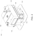
- FIG. 2 is a perspective view of an immersion station 120 according to an embodiment of the present invention.
- the immersion station 120 includes a generally rectangular upper housing 122 enclosing an immersion chamber. Below the upper housing 122 is a tank 124 in which a solvent bath is maintained. The solvent bath stored in the tank 124 may include one or more solvents which are used in semiconductor processing.
- the housing 122 includes a door 126 through which individual wafers can be transferred into and out of the station. Within the immersion station 120, the wafers are received in cassettes (not shown in FIG. 2 ) that secure the wafers.
- the internal cassettes can be moved vertically via a cassette Z-drive 128 (See, Fig.
- the enclosure 122 can also include a view port 132 for allowing process engineers to monitor the immersion process.
- FIG. 3 is a perspective view of an embodiment of the self-cleaning immersion station 120 according to an embodiment of the present invention with the top portion of the enclosure removed.
- station 120 includes a spray bar 125 coupled to the housing via a pivotable coupling 127.
- the pivotable coupling 127 can be positioned near to and/or on the side of the housing near to the door 126 ( FIG. 2 ) of the immersion station (not explicitly shown in FIG. 3 )
- the spray bar includes 125 is coupled to a plurality of nozzles, e.g., 131, 133 that are adapted to spray cleaning fluid at a selected pressure onto a wafer 190 after the wafer has been lifted from the solvent tank 124 and is being removed from the immersion station after a soaking process.
- the nozzles 131, 133 are distributed over the majority of the length of the spray bar 125 to cover the entire width of the substrate with spray to remove material from the surface of the wafer.
- the spray bar 125 can also be rotated via the pivotable coupling 127 fixed or movable at a selective speed provide to vary the distribution of spray.
- the pressure can range from a light liquid dispense of about 1 to 10 psi, to a medium pressure of about 50 to about 150 psi, to a high-pressure spray of about 2500 to about 3500 psi. Material or residual small particles (e.g., under 25 ⁇ m) suspended in the solvent that adhere to the wafer surface are removed by the spray.
- the spray can contribute solvent for replacing fluid that is often lost from the bath due to transfer or evaporation.
- a variety of different types of nozzles can be used in the spray bar, including, but not limited to fan, cone, and fan and needle nozzles.
- the spray type, pressure, flow rate and temperature are controllable parameters that can be set based on a specific processing recipe.
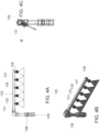
- FIGS. 4A, 4B and 4C illustrate side, perspective and end views of an embodiment of the spray bar 125 according to the present invention.
- FIG. 4A shows a spray bar 125 including five nozzles 131, 133, 135, 137, 139 arranged linearly along the length of the spray bar.
- nozzles 131, 133, 135, 137, 139 are fan nozzles that direct a spray in a diverging, fan-like manner.
- other combinations of nozzle types can be used.
- the nozzles 131-139 can pivot within an angular range ( ⁇ ) with respect to a vertical axis.
- the pivoting aids the dislodging of material as a component of the force of the spray is directed horizontally, providing a shearing action to remove residual debris.
- the spray bar has 125 an internal fluid conduit and is coupled to an inlet 129 through which pressurized solvent is supplied through the conduit to the nozzles 131-139.
- the spray bar 125 can include more than one inlet for delivering different fluids (e.g., solvent, water or otherwise).
- the height of the spray bar 125 can be adjusted using an adjustable fastener such as a locking nut 136.
- FIG. 5A is a top plan view and FIG. 5B is a side view depicting a wafer 190 in the process being removed from the immersion station 120 after having been released from the holding cassette by a handler (not shown).
- Paddle 185 is shown supporting the wafer from underneath as the wafer is transferred. The extraction of the wafer occurs directly under the spray bar so that the plurality of nozzles 131-139 can direct maximal spray onto the wafer surface for dislodging adhered solids and to rinse contaminated, debris-filled solvent from the wafer.
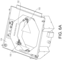
- FIGS. 6A , 6B and 6C illustrate an embodiment of an immersion tank having a tank rinse assembly for self-cleaning according to the present invention.
- FIG. 6A is a perspective top view of an immersion station with the upper housing removed and shows a cleaning fluid delivery tube 192 that extends circumferentially around the inner perimeter of the tank 124.
- a plurality of nozzles e.g., 193, 195 are attached to, and receive fluid from, the delivery tube 192.
- the delivery tube 192 is coupled to a cleaning fluid supply source (not shown).
- Nozzles 193, 195 which may be, but are not limited to, fan nozzles as shown, direct a pressurized cleaning spray onto the inner walls of the tank 124 and also toward the solvent bath held within the tank.
- the sprayed cleaning fluid dislodges the particles from the wall and/or into the solvent bath.
- the nozzles can be arranged to direct the particles along the floor and into the drain. In some cases, for example when a small number of nozzles are employed, it may be preferable to use fan nozzles which emit a wide-angle to cover the inner surfaces of the tank with cleaning fluid.
- the spray from nozzles 193, 195 is directed toward the solvent bath and agitates the chemicals and suspended debris within the bath.
- the agitation helps break larger debris particles into smaller particles which are able to pass through filters positioned in the drain path 196 and exit from the immersion station.
- the bottom surface of the tank 194 can be sloped to facilitate movement of particles coming out of suspension toward drain path 196.
- the agitation of the solvent bath can also aided by the one or more ultrasonic actuators 130 which induce ultrasonic vibrations via one or more walls of the tank, as shown in FIG. 6B .
- FIG. 6C is a perspective view of the self-cleaning assembly 191 shown by itself.
- a cleaning fluid inlet 198 feeds fluid to the tube 192, which runs circumferentially in a form that follows the inner contour of the tank, which in the depicted case is octagonal.
- FIG. 6C shows the entire track of the tube with four equally-spaced nozzles 193, 195, 197, 199 positioned to direct wide-angle sprays onto the inner surfaces of the tank and the surface of the solvent bath.
- the tube can be configured differently, for example, in a circular shape.
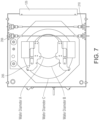
- FIG. 7 illustrates a cut-away top view of an embodiment of the immersion station 120 that includes through-beam sensors for determining the position of wafers held within the immersion tank, and for determining whether a wafer has been moved toward the door of the immersion station for transfer.
- wafers of a variety of diameters are shown positioned in an immersion tank 124 and confined within a secure by a wafer cassette 205.
- the wafer cassette 205 contacts and supports the edges of the wafer such that the robot arm can transfer wafers into and out of the immersion station.
- a first sensor 208 which may comprise a laser beam emitter (e.g., infrared or visible) positioned on one side of tank and a laser detector positioned on the opposite side, is positioned to intersect the wafers and provides a signal for determining the wafer presence and position according to the timing or position at which the laser beam is reflected or blocked. Sensor 208 is blocked by the wafer as the cassette is indexed allowing the cassette to be mapped.
- a second sensor 210 is positioned near to but further from the center of the tank towards the door 126 of the immersion station. The second sensor 210 may also comprise a laser beam emitter and detector positioned on opposite sides of the tank. The second sensor is positioned to detect a wafer that has been shifted toward the door by the handler or otherwise. When the laser beam of the second sensor 210 is blocked by a wafer, it is determined that the wafer is moved or slid out such that an error is detected before door 126 is closed.
- a laser beam emitter e.g., infrare
- FIG. 8 shows an embodiment of a self-cleaning lift-off station 140 according to an embodiment of the present invention.
- the station 140 comprises a rectangular chamber 142 having a number of different spray devices for lifting-off metal and/or other material from photoresist layers from wafer surfaces and for thoroughly cleaning the inner surfaces of the chamber.
- a door 143 At the front of the chamber 142 is a door 143 through which wafers are transferred into an out of the chamber.
- An overhead shower sprayer 144 is positioned toward the top of chamber, for example, by a cantilevered coupling as shown, and includes a plurality of spray nozzles 169 (e.g., 3, 4, 5, etc.) positioned around the perimeter of a fixture, which may be circular in shape as shown, or have other shapes.
- the nozzles 169 can also be adjustable in that they can pivot to allow the spray direction to be slightly altered.
- An exemplary embodiment of an overhead shower sprayer 144 is shown in FIG. 9 .
- Additional pivotable nozzle manifolds 145, 146, 147 are positioned on three inner walls of the chamber.
- An exemplary embodiment of one of the nozzle manifolds, e.g., 145 is shown in FIG. 10 .
- the manifold 145 has a fluid inlet 149 arranged on an upwardly tilted front surface, a plurality of nozzles, e.g., 151, 152 arranged on a bottom surface front and one or more nozzles arranged on side 153, and back surfaces 154.
- the nozzle manifolds having a large number of nozzles arranged on different surfaces and at various angles, are configured to apply a rinse spray over a wide area of the chamber 142 and cover as much inner surface area as possible.
- the nozzles 151, 152 can be capped in they are not in-use.
- the manifolds 145, 146, 147 can have the same structure and as shown, can be arranged along one side of the rectangular chamber 142.
- one of the manifolds 145, 146, 147 can also be used as part of a spray mechanism for spraying a splash shield 148 that is part of self-cleaning lift-off station 140.
- the splash shield 148 is a structure that surrounds a substrate (e.g., wafer chuck) on which the wafer rests.
- the splash shield 148 is annular shaped as shown and many times, can be raised or lowered.
- a manifold 400 can be provided that has a similar or the same structure as the manifolds 145, 146, 147 and therefore, like elements are numbered alike.
- the manifold 400 includes an elongated spray element 410 that has a conduit form and has a first end that is sealingly coupled to the nozzle 151 and the opposite second end that is sealingly coupled to the nozzle 153.
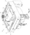
- the elongated spray element 410 has a bent structure so as to protrude inwardly toward the center of the rectangular chamber 142 and more specifically, the elongated spray element 410 has an arcuate section 420 that is positioned above an arcuate segment of the splash shield 148.
- the elongated spray element 410 can thus be in the form of a rinse tube for cleaning the top of the splash shield 148.
- the downward spray pattern is shown by the series of parallel lines extending from the underside of the elongated spray element 410 to the splash shield 148 for cleaning thereof.
- optimal spray coverage within the rectangular chamber 142 is achieved.
- the lift-off station preferably includes a swivel sprayer 155 coupled to an arm 156 that pivots in the horizontal plane (in the other words, the arm 157 can rotate about a pivot axis so as to position the arm 156 in a desired location which can be a location that is directed inward towards a center of the equipment housing as described with reference to FIG. 18 .
- FIG 11 is a perspective view of an exemplary embodiment of swivel sprayer 155 and shows a rotating spray head 157 joined via collar 158 to one or more spray nozzles 159 positioned at the end of the pivotable arm 156.
- Rotating spray head 157 can be implemented using a commonly-available landscape sprayer that provides a full 360° spray.
- the spray coverage of the head 157 is generally a circle of a given diameter which depends on the construction of the nozzle of the head 157.
- the combination of sprayers is designed to be able to direct sprays of cleaning for to all of the wall surfaces and components within the chamber 142.
- more or less sprayers can be provided in any suitable combination to remove material deposited on surfaces within the chamber. It will be appreciated that the rotating spray head 157 is positioned so as to spray upward, while the one or more spray nozzles 159 spray downward.
- FIGS. 17 and 18 illustrate a dual swivel sprayer that includes a pair of rotating spray heads and does not includes the one or more spray nozzles 159 shown in FIG. 11 .
- a swivel sprayer 200 is shown in FIGS. 17 and 18 that is similar to the swivel sprayer 155 but includes the aforementioned differences and more particularly, the swivel sprayer 200 pivots in the horizontal plane (so as to have a sweeping action).
- the swivel sprayer 200 includes a first rotating spray head 202 and a second rotating spray head 204.
- the first rotating spray head 202 and the second rotating spray head 204 can be similar to the rotating spray head 157 and thus, each is configured to spray liquid in a 360 degree spray pattern.
- the first and second rotating spray heads 202, 204 can be the same type of head in that they each have the same 360 degree spray pattern (i.e., they spray a circle having a prescribed diameter).
- the first rotating spray head 202 has a first fluid conduit formed in a first arm 205 for delivering fluid to the head 202 and the second rotating spray head 204 has a second fluid conduit formed in a second arm 207 for delivering fluid to the head 204.
- the two conduits are maintained separately. As shown in FIG.
- the first rotating spray head 202 can be located a first distance (first radius) from a vertical post 210 from which the arms 205, 207 extend and the second rotating spray head 204 is located a second distance from the vertical post 210, with the first distance being greater than the second distance.
- the arms 205, 207 and heads 202, 204 rotate about the vertical post 210. Both heads 202, 204 point down to project the sprayed liquid downward.
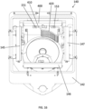
- FIG. 18 shows the swivel sprayer 200 in an in-use position in which the arms 205, 207 are positioned inwardly and centrally within the housing (e.g., at a location over the wafer chuck).
- the spray patterns of the heads 202, 204 are selected such that the two circular spray patterns, labeled C1 and C2, at least partially overlap as shown and when combined, the two circular shaped spray coverage covers a substantial inside area of the housing (station), thereby ensuring that the equipment and associated surfaces are cleaned.
- the arms 205, 207 are laterally spaced apart from one another and can be straight in shape or as shown, the distal end portion of the arm 205 can be curved (bent). It will be understood that the spray coverage shown in FIG. 18 is merely exemplary and the sizes and location of the circles can vary depending on the type of spray heads and other parameters, such as tank size, etc.
- the circles C1 and C2 depicting said spray coverage should have the same diameter. Any portion of the housing that is not within the spray coverage of C1, C2 can be addressed using another spray device, such as the ones described herein. In this way, with two or more sprayers, complete spray coverage within the housing is achieved.
- Embodiments of the self-cleaning lift-off station according to present invention can also include a useful feature for entirely removing debris that might otherwise clog filters or adhere to wafer and chamber surfaces.
- a vacuum-assisted separator sprayer 160 is positioned with spray end positioned toward the front of the chamber near door 143.
- FIG. 12A is a bottom perspective view that shows the vacuum-assisted separator 160 sprayer in greater detail.
- a main arm 161 is attached to an arm drive (not shown).
- the main arm 161 makes an elbow turn or coupling to a distal arm 162 that holds a dispense head 163.
- a skirt 164 encircles the elbow joint where the main arm 161 and distal arm 162 join in order to prevent fluids from entering the arm drive.
- the dispense head includes first and second nozzles 165, 166.
- first nozzle 165 is adapted to generate a fan spray
- nozzle 166 is adapted to generate a needle spray, or vice versa.
- nozzles 165, 166 can be adapted to generate the same type of spray or sprays other than a fan and needle spray.
- solvent is supplied to nozzles 165, 166 at high pressure to provide enough force to dislodge the metal or other material film and underlying resist from wafer substrates during a lift-off process.
- a collar 167 is coupled to the distal arm 162 as well as to a suction conduit 168.
- a suction head 170 coupled to the suction conduit 168 is positioned adjacent to the dispense head.
- the suction head 170 is adapted to generate a vacuum suction force by a Venturi body 172 coupled to a nitrogen supply line via nitrogen inlet 173.
- Venturi body 172 nitrogen gas is forced into a narrow passageway from a larger passageway, which as is known in the art, generates a high-speed flow and a pressure differential in a direction perpendicular to the gas flow.
- the suction head 170 includes an inlet 175 that is positioned to draw in, via the suction force generated by the Venturi body 172, material dislodged by the high-pressure sprays generated by the nozzles 165, 166 at the dispense head 163.
- Lift-off materials, some solvent from the wafer surface and some amount of air that is entrapped by the suction force enters the inlet and flows through the suction conduit to a drain (not shown in FIG. 12A ).
- the rapid removal of the debris into the suction conduit not only prevents the accumulation of the debris within the station chamber 142, but also prevents the debris from being dragged along the surface of the wafer.
- FIG. 12B is an end view of the vacuum-assisted separator which illustrates a jet of high-pressure solvent 177 emitted from a nozzle 166 impacting a wafer 190. As shown, fluid and lift-off material is captured by the suction force and enters the inlet 175 of suction head 170.
- FIG. 12C is a cross-sectional view of the vacuum-assisted portion of separator 160. This view shows nitrogen inlet 173 of the Venturi body and the narrow opening 178 through which the nitrogen is forced to generate the high-speed flow and pressure differential. The suction flow 176 is shown by arrows within the suction conduit 168. Air, nitrogen, lift-off material and solvent exits the suction conduit toward a drain.
- FIG. 13 is a perspective view of an alternative embodiment of a vacuum-assisted separator 220 according to the present invention.
- the separator includes a coiled supply line that provides pressurized solvent to a dispense head 222 including a fan nozzle 224.
- the end of the nozzle 224 is coupled to a first side of spacer 225, and the second side of the spacer 225 is coupled to a suction head 226.
- the nozzle 224 is in line with and directs spray through the suction head 226.
- Suction head 226 has a main opening at the bottom through which spray can be directed onto a wafer surface, and includes a side opening into a suction conduit 228 that is coupled to a vacuum source.
- a Venturi body is not directly coupled to the suction head 226, rather, the suction conduit 228 is coupled to a downstream blower or other conventional vacuum-generating device 229.
- the suction conduit 228 is coupled to a downstream blower or other conventional vacuum-generating device 229.
- lift off material is forcibly ejected upwardly from the surface into the suction head 226 and becomes entrained by the suction emanating from the suction conduit at side exit of the suction head. The material is drawn off through the suction conduit to a drain (not shown).
- FIG. 14A is a magnified schematic illustration of how the vacuum-assisted separator aids in drawing debris from the wafer surface into a suction path, which aids in preventing build-up of residual material in the lift-off station.
- a nozzle 165 is enveloped within a suction head which is cut at an angle so that both the suction head main opening 230, and the adjacent opening 232 to the suction conduit through which suction is applied, are positioned near to the surface of a wafer 190.
- the nozzle 165 directs a fan of high-pressure solvent spray toward the surface of a wafer 190, the spray forcibly breaks off and atomizes the lift-off material.
- the overwhelming majority particles of debris 233 that is dislodged from the wafer surface enters and becomes entrained in the suction flow within the suction head, due to the close positioning of the suction head and applied vacuum to the wafer surface.
- FIG. 14B is a schematic illustration of debris removal using a vacuum-assisted separator that employs a Venturi body 172. Debris that is removed from the wafer 190 positioned within a chamber is drawn into the main opening of suction head 170 by the suction generated by nitrogen gas flow in the Venturi body. The suction conduit delivers the debris to a drain 240 that flows into a tank 245 with a filter 247.
- FIG. 14C is a schematic illustration of debris removal using a vacuum-assisted separator that employs a blower 250 to generate suction. In this embodiment, suction is generated from a blower that is fluidly coupled to the suction head via a tank 255.
- Debris drawn through the suction head is similarly drawn through a conduit into a filter 257 positioned in the tank.
- These embodiments illustrate how rather than being ejected into the spaces and surfaces within the lift-off chamber, embodiments of the vacuum-assisted separator redirect lift-off debris into a drain and filter. The amount of debris that accumulates on the internal surfaces of the chamber is thereby reduced. Furthermore, any debris that is not captured by the vacuum-assisted separator can be washed from the internal surfaces by the numerous cleaning sprays employed in the lift-off station according to the embodiments of the present invention.
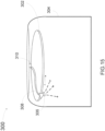
- FIG. 15 is a front view of an overhead track sprayer device 300 that may be used in embodiments of a lift-off station according to the present invention.
- the device includes a circular or elliptical track system 302 that may be attached to roof or dome of the station chamber 304.
- a nozzle 306 is positioned on the track and receives fluid from tubing 308 that may run through a seal 310 attached to the chamber and to a cleaning fluid supply source.
- the tubing swivels the nozzle 360° around the track by the force of the high-pressure fluid within the tubing. The swiveling allows the nozzle to cover the inner surfaces of the chamber with cleaning fluid to remove debris and leftover solvents.
- the tubing 308 can run from a valve to a fast-acting disconnect.
- a sealed swivel fitting at the center of the track 302 can be used to provide full rotation of the tubing 308 without twisting or kinking.
- the tubing 308 can be attached to the track 302 using rollers to reduce friction and provide consistent rotation.
Landscapes
- Engineering & Computer Science (AREA)
- Mechanical Engineering (AREA)
- Cleaning Or Drying Semiconductors (AREA)
- Electrical Discharge Machining, Electrochemical Machining, And Combined Machining (AREA)
- Polarising Elements (AREA)
Description
- The present application claims priority to and the benefit of
US patent application serial No. 62/687,643, filed June 20, 2018 - The present invention relates to semiconductor fabrication equipment and processing, and in particular, relates to a system and method for removing residues from processing equipment used in a wet treatment process, including solvent immersion and film lift-off stations.
- Semiconductor fabrication typically involves deposition of a mask or pattern which determines the components and the electrical connections on a substrate. One common masking technique involves depositing photoresist across a substrate surface and then selectively exposing a pattern on the photoresist. During wet treatment, the pattern is etched onto the substrate material by removal of the exposed sections (or alternatively by sections that were not exposed, depending on the type of photoresist). By chemical development both exposed photoresist and material underlying the exposed photoresist can then be chemically removed by immersion in a solvent, resulting in a patterned structure.
- To accommodate fabrication on substrates that are harder to remove by conventional solvent immersion, such as Gallium Arsenide (GaAs), photoresist can be deposited first, underneath subsequently deposited material that is harder to dissolve. When solvent is applied, the photoresist dissolves and layers overlying the photoresist can be removed, or lifted-off, as well. During both the immersion phase and subsequent lift-off phase, a considerable amount of debris and residue can accumulate. Additionally, during immersion incompletely dissolved materials build-up in the solvent bath and can also remain on the meniscus on the wafer surface.
- After immersion, the wafer is typically transferred to a spin chamber in which a high-pressure spray is applied to remove excess material and residual photoresist from the wafer. The residual debris tends to accumulate rapidly on walls of the spin chamber or in filters positioned in the fluid drain path, necessitating frequent cleaning of the spin chamber (e.g., several times per day). The time that the chambers spend offline reduces wafer throughput and the overall efficiency of the fabrication process. Furthermore, the high-pressure spray can damage the wafer surface as any adhering or trapped debris is dragged along by surface by the force of the spray.
- It would therefore be advantageous to adapt the semiconductor fabrication process to meet these challenges caused by the accumulation of residual resist and other dislodged material.
- It is with respect to these and other considerations that the disclosure made herein is presented. Anyway, it is worth noting also that
US 2004/074600 A1 , that relates to a wet etch system with overflow particle removing feature, discloses a wet etch system including a process tank having an inner etch bath chamber and an outer overflow chamber surrounding the etch bath chamber. A frame which is removably mounted on the process tank defines a diversion channel between the upper ends of the etch bath chamber and overflow chamber. The etch bath chamber receives a wafer-containing cassette, which displaces etchant from the etch bath chamber, through the diversion channel and into the overflow chamber, where the etchant is drained from the process tank. Particulate impurities leave the etch bath chamber, enter the overflow chamber and drain from the process tank with the overflow etchant. Fresh etchant is poured into the etch bath chamber prior to a subsequent etch cycle. A water spray loop may be provided in the overflow chamber for removing etch particles from the interior wall surfaces of the overflow chamber. Additionally,US 6 514 355 B1 , that relates to a method and apparatus for recovery of semiconductor wafers from a chemical tank, discloses a method for stopping chemical processing of a semiconductor wafer in an emergency included the steps of: 1) placing a chemical having a water concentration of about 92% or less in a tank; 2) processing a semiconductor wafer with the chemical in the process tank; 3) detecting a malfunction in the processing; 4) quick draining the chemical from the process tank; and 5) rinsing the wafer in the process tank with a rinsing material to stop chemical action. Optionally, the method may include recycling the drained chemical from a storage tank to the process tank for use in a subsequent process step. Also, a chemical processing system includes: 1) a process tank adapted to processing semiconductor wafers in a chemical having a water concentration of about 92% or less; 2) a control system adapted to detecting a malfunction in processing; 3) a drain valve adapted to quick draining the chemical in the process tank; 4) a storage tank adapted to storing the quick drained chemical; 5) a spray bar adapted to applying a rinsing material to the wafers in the process tank; and 6) a recycling mechanism adapted to returning the quick drained chemical to the process tank. -
US 2017/333958 A1 discloses a substrate liquid treatment apparatus that includes: a tank that stores a processing liquid; a circulation line connected to the tank, through which circulation line a circulation flow of the processing liquid that leaves the tank and then returns back to the tank; a processing unit that processes a substrate by supplying the processing liquid, distributed from the circulation line, to the substrate; a return line that returns, to the tank, the processing liquid discharged from the processing unit after being supplied to the substrate; a cleaning nozzle that discharges a cleaning liquid onto an inner wall surface of the tank to clean the inner wall surface by the cleaning liquid; and a cleaning line that supplies the cleaning liquid to the cleaning nozzle. -
US 2014/190530 A1 discloses a substrate cleaning apparatus capable of preventing a cleaning vessel from being corroded by a chemical liquid while constituting the cleaning vessel with a low-price material. The substrate cleaning apparatus includes: a cleaning vessel for holding a substrate therein; a substrate holder arranged in the cleaning vessel; a chemical liquid nozzle for supplying a chemical liquid onto the substrate held by the substrate holder; and a plurality of cleaning liquid nozzles for supplying a cleaning liquid onto an inner surface of the cleaning vessel. The inner surface of the cleaning vessel has been subjected to a hydrophilization treatment. -
US 2014/377951 A1 discloses an apparatus in accordance with the preamble ofclaim 1 and method for removing challenging polymer films and structures from semiconductor wafers. In particular, the method according toUS 2014/377951 A1 involves the use of a double soak and spray sequence with unique parameters and can be varied depending upon the application. The initial immersion step is used to initiate the swelling and dissolution of the polymer. The first spray step may include a high pressure needle to pierce through the top layer allowing more solvent to penetrate in the subsequent soak process. The second immersion can then penetrate further and faster allowing substantial penetration of the polymer by the solvent. The final high pressure spray proceeds to remove all of the polymer coating. The process ends with a final rinse and dry sequence. -
WO 03/095115 A1 KR 2012 0040466 A - The present invention concerns a semiconductor processing system comprising:
- an immersion station adapted for immersion of a wafer in solvent for removal of material, wherein an opening is formed in the immersion station through which the wafer can be removed from inside the immersion station; and
- a lift-off station adapted to completely remove material from the surface of the wafer and including a separator adapted to spray solvent at a high pressure spray onto the wafer surface;
- wherein:
- the immersion station is self-cleaning and includes a self-cleaning assembly adapted to spray cleaning fluid on internal surfaces of the immersion station;
- the immersion station further includes a first sprayer having a plurality of nozzles positioned to spray the wafer as it is transferred out of the immersion station, wherein the first sprayer comprises an elongated spray bar that is disposed proximate the opening formed in the immersion station, includes a plurality of nozzles positioned longitudinally along the spray bar and is configured to spray downward onto the wafer for removing suspended particles and solvent from a surface of the wafer as the wafer is removed from the opening formed in the immersion station;
- the lift-off station is self-cleaning and further includes at least one cleaning sprayer adapted to clean internal surfaces of the lift-off station; and
- the separator is vacuum-assisted and is adapted to spray the solvent while applying suction in the vicinity of the sprayed wafer surface to capture material dislodged by the spray.
- The present invention concerns also a method of semiconductor processing comprising:
- soaking a semiconductor wafer in a solvent bath within an immersion station to loosen a resist layer on the wafer;
- spraying an entire surface of the semiconductor wafer using a spray bar after removing the wafer from the solvent bath to remove suspended particles and solvent from the surface of the wafer as the wafer is removed from an opening formed in the immersion station, wherein the spray bar is disposed proximate the opening formed in the immersion station and includes a plurality of nozzles positioned longitudinally along the spray bar;
- spraying internal surfaces of the solvent tank using a plurality of spray nozzles located within the solvent tank;
- transferring the wafer from the immersion station to a lift-off station having a chamber;
- applying a high-pressure spray to the surface of the wafer to dislodge the resist layer and material overlying the resist;
- applying suction near to the surface of the wafer proximate a location at which the high-pressure spray is applied to the surface of the wafer to capture dislodged material in a suction stream; and
- removing the captured material from the chamber of the lift-off station.
- These and other aspects, features, and advantages can be appreciated from the following description of certain embodiments of the invention and the accompanying drawing figures and claims.
-
-
FIG. 1 is a top plan view of an integrated wet treatment system including self-cleaning features according to an embodiment of the present invention. -
FIG. 2 is a perspective view of a self-cleaning immersion station according to an embodiment of the present invention. -
FIG. 3 is a perspective view of a self-cleaning immersion station according to an embodiment of the present invention. In the view, the top portion of the housing has been removed. -
FIGS. 4A, 4B and 4C are side, perspective and end views of an embodiment of a spray bar with nozzles for an immersion station according to an embodiment of the present invention. -
FIGS. 5A and5B are top plan view and side views depicting a wafer in the process being removed from the immersion station according to an embodiment of the present invention. -
FIG. 6A is top perspective view of a self-cleaning immersion station according to an embodiment of the present invention with the upper housing removed. -
FIG. 6B is a cut-away side perspective view of an embodiment of a self-cleaning immersion station according to an embodiment of the present invention -
FIG. 6C is a perspective view of a self-cleaning assembly for an immersion station according to an embodiment of the present invention. -
FIG. 7 is a cut-away top view of an embodiment of the immersion station that includes through-beam sensors for determining the position of wafers held within and/or moving out of the immersion tank. -
FIG. 8 is a perspective view of an embodiment of a self-cleaning lift-off station according to an embodiment of the present invention. -
FIG. 9 is a perspective view of an embodiment of an overhead shower sprayer that may be used in a self-cleaning lift-off station according to the present invention. -
FIG. 10 is a perspective view of an embodiment of a nozzle manifold that may be used in a self-cleaning lift-off station according to the present invention. -
FIG. 11 is a perspective view of an embodiment of a swivel sprayer that may be used in a self-cleaning lift-off station according to the present invention. -
FIG. 12A is a bottom perspective view that shows an embodiment of a vacuum-assisted separator sprayer according to the present invention. -
FIG. 12B is an end view of an embodiment of a vacuum-assisted separator sprayer according to the present invention. -
FIG. 12C is a cross-sectional view of the vacuum-assisted portion of the separator sprayer according to an embodiment of the present invention. -
FIG. 13 is a perspective view of an alternative embodiment of a vacuum-assisted separator according to the present invention -
FIG. 14A is a magnified schematic illustration of how the vacuum-assisted separator aids in drawing debris from the wafer surface into a suction path. -
FIG. 14B is a schematic illustration of debris removal using a vacuum-assisted separator that employs a Venturi body. -
FIG. 14C is a schematic illustration of debris removal using a vacuum-assisted separator that employs a blower to generate suction. -
FIG. 15 is a front view of an embodiment of an overhead track rinse sprayer that may be used in in a self-cleaning lift-off station according to the present invention. -
FIG. 16 is a top perspective view of a self-cleaning immersion station according to another embodiment of the present invention. In the view, the top portion of the housing has been removed. -
FIG. 17 is a perspective view of another embodiment of a dual swivel sprayer that may be used in a self-cleaning lift-off station according to the present invention. -
FIG. 18 is a top plan view of a self-cleaning immersion station with the dual swivel sprayer ofFIG. 17 in an in-use position with the spray coverage of each sprayer head being depicted. - Embodiments of the present invention provide a system and method for removing debris from processing chambers during semiconductor fabrication. In particular, embodiments of the present invention include a self-cleaning immersion station that includes sets of sprayers for both cleaning the internal surfaces of the station chamber, and for spraying wafers as they are transferred out of the immersion station to remove suspended debris adhering to the wafer surface. Embodiments of the present invention also include a self-cleaning lift-off station that includes several types of sprays for cleaning residual debris and solvent from the internal surfaces of the lift-off station chamber, and a vacuum-assisted separator that draws of lift-off material into a suction path as the material is forcibly dislodged from the wafer surface by a high-pressure spray. Collectively, the sprayers and other devices that are added to the immersion and lift-off stations prevent the rapid build-up of debris within the chambers and dramatically reduce the frequency with which the stations need to be brought off-line for cleaning and maintenance.
-
FIG. 1 is a top plan view of an integrated wettreatment processing system 100 according to an embodiment of the present invention. The integrated system contains load ports for receiving and outputting wafer substrates into and out of the system. Within the system are disposed a number of stations or chambers in which specific processes are performed on wafer substrates. Typically, the wafers are processed by in a particular order, starting, for example, with immersion in a first chamber, followed by metal lift-off in a second chamber, and drying in a third chamber. A robot arm transfers wafers between the stations of the integrated system. More specifically, inFIG. 1 , an integratedwet processing system 100 includes arectangular enclosure 105 that houses several processing stations.Load port 110 is adapted to receive cassettes housing one or more semiconductor wafers from other parts of the fabrication facility.Load port 112, situated on the same side of the enclosure, is adapted to receive cassettes including wafers that have been processed and are ready to be transferred out of thesystem 100. Alternatively, the wafers can be returned to the same cassette. -
Integrated system 100 includes a number of processing stations arranged within theenclosure 105 including animmersion station 120 adapted for soaking wafers in a solvent bath to loosen resist layers, metal layers, or any suitable layers; a lift-off station 140 adapted to remove residual resist and overlying metallic films from the wafer; and a rinsedry station 160 adapted for removing any remaining solvent or other fluids from the wafer surface. Arobot arm 180 is adapted to securely hold and move individual wafers between the processing stations and the cassettes. In some embodiments, the robot arm includes apaddle 185 that is supplied with a Venturi vacuum stream. The vacuum stream enables a wafer to be secured in relation to the paddle without direct contact between the wafer and the paddle surface, preventing damage to the wafer surface. Theintegrated system 100 may also include one or more user control units, e.g., 187 that allow process engineers to set various parameters of the system, such as length of immersion time, and spray pressure, among numerous other control parameters. -
FIG. 2 is a perspective view of animmersion station 120 according to an embodiment of the present invention. Theimmersion station 120 includes a generally rectangularupper housing 122 enclosing an immersion chamber. Below theupper housing 122 is atank 124 in which a solvent bath is maintained. The solvent bath stored in thetank 124 may include one or more solvents which are used in semiconductor processing. Thehousing 122 includes adoor 126 through which individual wafers can be transferred into and out of the station. Within theimmersion station 120, the wafers are received in cassettes (not shown inFIG. 2 ) that secure the wafers. The internal cassettes can be moved vertically via a cassette Z-drive 128 (See,Fig. 1 ) (which may include rods, interconnectors and other components not shown) to move the cassette downward to soak the wafer intank 124, and to lift the cassettes out of the tank after immersion.Ultrasonic actuators 130 may be coupled to thetank 124 for vibrating the solvent bath, which helps force solvent though the small openings in the photoresist layers, aiding in the dissolving of photoresist material. Theenclosure 122 can also include aview port 132 for allowing process engineers to monitor the immersion process. -
FIG. 3 is a perspective view of an embodiment of the self-cleaningimmersion station 120 according to an embodiment of the present invention with the top portion of the enclosure removed. As shown,station 120 includes aspray bar 125 coupled to the housing via apivotable coupling 127. Thepivotable coupling 127 can be positioned near to and/or on the side of the housing near to the door 126 (FIG. 2 ) of the immersion station (not explicitly shown inFIG. 3 ) The spray bar includes 125 is coupled to a plurality of nozzles, e.g., 131, 133 that are adapted to spray cleaning fluid at a selected pressure onto awafer 190 after the wafer has been lifted from thesolvent tank 124 and is being removed from the immersion station after a soaking process. Thenozzles spray bar 125 to cover the entire width of the substrate with spray to remove material from the surface of the wafer. Thespray bar 125 can also be rotated via thepivotable coupling 127 fixed or movable at a selective speed provide to vary the distribution of spray. Depending on the residual material and device structure the pressure can range from a light liquid dispense of about 1 to 10 psi, to a medium pressure of about 50 to about 150 psi, to a high-pressure spray of about 2500 to about 3500 psi. Material or residual small particles (e.g., under 25 µm) suspended in the solvent that adhere to the wafer surface are removed by the spray. In addition to dislodging adhering particles, the spray can contribute solvent for replacing fluid that is often lost from the bath due to transfer or evaporation. A variety of different types of nozzles can be used in the spray bar, including, but not limited to fan, cone, and fan and needle nozzles. The spray type, pressure, flow rate and temperature are controllable parameters that can be set based on a specific processing recipe. -
FIGS. 4A, 4B and 4C illustrate side, perspective and end views of an embodiment of thespray bar 125 according to the present invention.FIG. 4A , shows aspray bar 125 including fivenozzles nozzles FIGS. 4B and 4C , the nozzles 131-139 can pivot within an angular range (α) with respect to a vertical axis. The pivoting aids the dislodging of material as a component of the force of the spray is directed horizontally, providing a shearing action to remove residual debris. The spray bar has 125 an internal fluid conduit and is coupled to aninlet 129 through which pressurized solvent is supplied through the conduit to the nozzles 131-139. In other embodiments, thespray bar 125 can include more than one inlet for delivering different fluids (e.g., solvent, water or otherwise). The height of thespray bar 125 can be adjusted using an adjustable fastener such as a lockingnut 136. -
FIG. 5A is a top plan view andFIG. 5B is a side view depicting awafer 190 in the process being removed from theimmersion station 120 after having been released from the holding cassette by a handler (not shown).Paddle 185 is shown supporting the wafer from underneath as the wafer is transferred. The extraction of the wafer occurs directly under the spray bar so that the plurality of nozzles 131-139 can direct maximal spray onto the wafer surface for dislodging adhered solids and to rinse contaminated, debris-filled solvent from the wafer. -
FIGS. 6A ,6B and6C illustrate an embodiment of an immersion tank having a tank rinse assembly for self-cleaning according to the present invention.FIG. 6A is a perspective top view of an immersion station with the upper housing removed and shows a cleaningfluid delivery tube 192 that extends circumferentially around the inner perimeter of thetank 124. A plurality of nozzles e.g., 193, 195 are attached to, and receive fluid from, thedelivery tube 192. Thedelivery tube 192 is coupled to a cleaning fluid supply source (not shown).Nozzles tank 124 and also toward the solvent bath held within the tank. With respect to debris that adheres to the tank, the sprayed cleaning fluid dislodges the particles from the wall and/or into the solvent bath. Alternatively, the nozzles can be arranged to direct the particles along the floor and into the drain. In some cases, for example when a small number of nozzles are employed, it may be preferable to use fan nozzles which emit a wide-angle to cover the inner surfaces of the tank with cleaning fluid. - Referring to the cut-away side view of
FIG. 6B , the spray fromnozzles drain path 196 and exit from the immersion station. The bottom surface of thetank 194 can be sloped to facilitate movement of particles coming out of suspension towarddrain path 196. The agitation of the solvent bath can also aided by the one or moreultrasonic actuators 130 which induce ultrasonic vibrations via one or more walls of the tank, as shown inFIG. 6B . -
FIG. 6C is a perspective view of the self-cleaningassembly 191 shown by itself. A cleaningfluid inlet 198 feeds fluid to thetube 192, which runs circumferentially in a form that follows the inner contour of the tank, which in the depicted case is octagonal. In contrast to the cut-away views shown inFIGS. 6A and6B ,FIG. 6C shows the entire track of the tube with four equally-spacednozzles -
FIG. 7 illustrates a cut-away top view of an embodiment of theimmersion station 120 that includes through-beam sensors for determining the position of wafers held within the immersion tank, and for determining whether a wafer has been moved toward the door of the immersion station for transfer. As shown, wafers of a variety of diameters (diameters A, B and C) are shown positioned in animmersion tank 124 and confined within a secure by awafer cassette 205. Thewafer cassette 205 contacts and supports the edges of the wafer such that the robot arm can transfer wafers into and out of the immersion station. Afirst sensor 208, which may comprise a laser beam emitter (e.g., infrared or visible) positioned on one side of tank and a laser detector positioned on the opposite side, is positioned to intersect the wafers and provides a signal for determining the wafer presence and position according to the timing or position at which the laser beam is reflected or blocked.Sensor 208 is blocked by the wafer as the cassette is indexed allowing the cassette to be mapped. Asecond sensor 210 is positioned near to but further from the center of the tank towards thedoor 126 of the immersion station. Thesecond sensor 210 may also comprise a laser beam emitter and detector positioned on opposite sides of the tank. The second sensor is positioned to detect a wafer that has been shifted toward the door by the handler or otherwise. When the laser beam of thesecond sensor 210 is blocked by a wafer, it is determined that the wafer is moved or slid out such that an error is detected beforedoor 126 is closed. - The immersion process causes photoresist layers to swell, and serves as a preparation for a material lift-off process which takes place in the lift-off station, to which wafers are transferred by the robot arm after immersion. In the lift-off station, metal or other materials deposited over a resist layer are "lifted-off" and removed from the wafer.
FIG. 8 shows an embodiment of a self-cleaning lift-off station 140 according to an embodiment of the present invention. Thestation 140 comprises arectangular chamber 142 having a number of different spray devices for lifting-off metal and/or other material from photoresist layers from wafer surfaces and for thoroughly cleaning the inner surfaces of the chamber. At the front of thechamber 142 is adoor 143 through which wafers are transferred into an out of the chamber. Anoverhead shower sprayer 144 is positioned toward the top of chamber, for example, by a cantilevered coupling as shown, and includes a plurality of spray nozzles 169 (e.g., 3, 4, 5, etc.) positioned around the perimeter of a fixture, which may be circular in shape as shown, or have other shapes. Thenozzles 169 can also be adjustable in that they can pivot to allow the spray direction to be slightly altered. An exemplary embodiment of anoverhead shower sprayer 144 is shown inFIG. 9 . Additionalpivotable nozzle manifolds FIG. 10 . The manifold 145 has afluid inlet 149 arranged on an upwardly tilted front surface, a plurality of nozzles, e.g., 151, 152 arranged on a bottom surface front and one or more nozzles arranged onside 153, and back surfaces 154. The nozzle manifolds, having a large number of nozzles arranged on different surfaces and at various angles, are configured to apply a rinse spray over a wide area of thechamber 142 and cover as much inner surface area as possible. Thenozzles manifolds rectangular chamber 142. - Alternatively, one of the
manifolds off station 140. As is known, the splash shield 148 is a structure that surrounds a substrate (e.g., wafer chuck) on which the wafer rests. The splash shield 148 is annular shaped as shown and many times, can be raised or lowered. More specifically, a manifold 400 can be provided that has a similar or the same structure as themanifolds elongated spray element 410 that has a conduit form and has a first end that is sealingly coupled to thenozzle 151 and the opposite second end that is sealingly coupled to thenozzle 153. Theelongated spray element 410 has a bent structure so as to protrude inwardly toward the center of therectangular chamber 142 and more specifically, theelongated spray element 410 has anarcuate section 420 that is positioned above an arcuate segment of the splash shield 148. Along an underside of theelongated spray element 410, there is a plurality of holes (spray holes) through which the liquid spray is discharged in a downward direction toward the splash shield 148. Theelongated spray element 410 can thus be in the form of a rinse tube for cleaning the top of the splash shield 148. InFIG. 16 , the downward spray pattern is shown by the series of parallel lines extending from the underside of theelongated spray element 410 to the splash shield 148 for cleaning thereof. In combination with the other spray systems described herein, including the spray system shown inFIGS. 17 and18 , optimal spray coverage within therectangular chamber 142 is achieved. - In addition to the shower spray and side nozzle manifolds, the lift-off station preferably includes a
swivel sprayer 155 coupled to anarm 156 that pivots in the horizontal plane (in the other words, thearm 157 can rotate about a pivot axis so as to position thearm 156 in a desired location which can be a location that is directed inward towards a center of the equipment housing as described with reference toFIG. 18 .FIG 11 is a perspective view of an exemplary embodiment ofswivel sprayer 155 and shows arotating spray head 157 joined viacollar 158 to one ormore spray nozzles 159 positioned at the end of thepivotable arm 156. Rotatingspray head 157 can be implemented using a commonly-available landscape sprayer that provides a full 360° spray. In other words, the spray coverage of thehead 157 is generally a circle of a given diameter which depends on the construction of the nozzle of thehead 157. The combination of sprayers is designed to be able to direct sprays of cleaning for to all of the wall surfaces and components within thechamber 142. In alternative aspects, more or less sprayers can be provided in any suitable combination to remove material deposited on surfaces within the chamber. It will be appreciated that the rotatingspray head 157 is positioned so as to spray upward, while the one ormore spray nozzles 159 spray downward. - The
swivel sprayer 155 ofFIG. 11 can be thought of as being a single swivel sprayer since it includes a singlerotating spray head 157. In contrast,FIGS. 17 and18 illustrate a dual swivel sprayer that includes a pair of rotating spray heads and does not includes the one ormore spray nozzles 159 shown inFIG. 11 . More specifically, aswivel sprayer 200 is shown inFIGS. 17 and18 that is similar to theswivel sprayer 155 but includes the aforementioned differences and more particularly, theswivel sprayer 200 pivots in the horizontal plane (so as to have a sweeping action). Theswivel sprayer 200 includes a firstrotating spray head 202 and a secondrotating spray head 204. The firstrotating spray head 202 and the secondrotating spray head 204 can be similar to therotating spray head 157 and thus, each is configured to spray liquid in a 360 degree spray pattern. The first and second rotating spray heads 202, 204 can be the same type of head in that they each have the same 360 degree spray pattern (i.e., they spray a circle having a prescribed diameter). The firstrotating spray head 202 has a first fluid conduit formed in afirst arm 205 for delivering fluid to thehead 202 and the secondrotating spray head 204 has a second fluid conduit formed in asecond arm 207 for delivering fluid to thehead 204. The two conduits are maintained separately. As shown inFIG. 17 , the firstrotating spray head 202 can be located a first distance (first radius) from avertical post 210 from which thearms rotating spray head 204 is located a second distance from thevertical post 210, with the first distance being greater than the second distance. Thearms vertical post 210. Both heads 202, 204 point down to project the sprayed liquid downward.FIG. 18 shows theswivel sprayer 200 in an in-use position in which thearms heads FIG. 18 , thearms arm 205 can be curved (bent). It will be understood that the spray coverage shown inFIG. 18 is merely exemplary and the sizes and location of the circles can vary depending on the type of spray heads and other parameters, such as tank size, etc. As mentioned, when the spray heads 202, 204 have the same 360 spray coverage, the circles C1 and C2 depicting said spray coverage should have the same diameter. Any portion of the housing that is not within the spray coverage of C1, C2 can be addressed using another spray device, such as the ones described herein. In this way, with two or more sprayers, complete spray coverage within the housing is achieved. - Embodiments of the self-cleaning lift-off station according to present invention can also include a useful feature for entirely removing debris that might otherwise clog filters or adhere to wafer and chamber surfaces. A vacuum-assisted
separator sprayer 160 is positioned with spray end positioned toward the front of the chamber neardoor 143.FIG. 12A is a bottom perspective view that shows the vacuum-assistedseparator 160 sprayer in greater detail. As shown, amain arm 161 is attached to an arm drive (not shown). Themain arm 161 makes an elbow turn or coupling to adistal arm 162 that holds a dispensehead 163. Askirt 164 encircles the elbow joint where themain arm 161 anddistal arm 162 join in order to prevent fluids from entering the arm drive. The dispense head includes first andsecond nozzles first nozzle 165 is adapted to generate a fan spray, andnozzle 166 is adapted to generate a needle spray, or vice versa. In other embodiments,nozzles nozzles - In the embodiment depicted, a
collar 167 is coupled to thedistal arm 162 as well as to asuction conduit 168. Asuction head 170 coupled to thesuction conduit 168 is positioned adjacent to the dispense head. In the depicted embodiment, thesuction head 170 is adapted to generate a vacuum suction force by aVenturi body 172 coupled to a nitrogen supply line vianitrogen inlet 173. WithinVenturi body 172, nitrogen gas is forced into a narrow passageway from a larger passageway, which as is known in the art, generates a high-speed flow and a pressure differential in a direction perpendicular to the gas flow. Thesuction head 170 includes aninlet 175 that is positioned to draw in, via the suction force generated by theVenturi body 172, material dislodged by the high-pressure sprays generated by thenozzles head 163. Lift-off materials, some solvent from the wafer surface and some amount of air that is entrapped by the suction force enters the inlet and flows through the suction conduit to a drain (not shown inFIG. 12A ). The rapid removal of the debris into the suction conduit not only prevents the accumulation of the debris within thestation chamber 142, but also prevents the debris from being dragged along the surface of the wafer. -
FIG. 12B is an end view of the vacuum-assisted separator which illustrates a jet of high-pressure solvent 177 emitted from anozzle 166 impacting awafer 190. As shown, fluid and lift-off material is captured by the suction force and enters theinlet 175 ofsuction head 170.FIG. 12C is a cross-sectional view of the vacuum-assisted portion ofseparator 160. This view showsnitrogen inlet 173 of the Venturi body and thenarrow opening 178 through which the nitrogen is forced to generate the high-speed flow and pressure differential. Thesuction flow 176 is shown by arrows within thesuction conduit 168. Air, nitrogen, lift-off material and solvent exits the suction conduit toward a drain. -
FIG. 13 is a perspective view of an alternative embodiment of a vacuum-assistedseparator 220 according to the present invention. The separator includes a coiled supply line that provides pressurized solvent to a dispensehead 222 including afan nozzle 224. The end of thenozzle 224 is coupled to a first side ofspacer 225, and the second side of thespacer 225 is coupled to asuction head 226. According to this arrangement, thenozzle 224 is in line with and directs spray through thesuction head 226.Suction head 226 has a main opening at the bottom through which spray can be directed onto a wafer surface, and includes a side opening into asuction conduit 228 that is coupled to a vacuum source. In this embodiment, a Venturi body is not directly coupled to thesuction head 226, rather, thesuction conduit 228 is coupled to a downstream blower or other conventional vacuum-generatingdevice 229. In operation, when the high-pressure spray ofnozzle 224 impacts the wafer, lift off material is forcibly ejected upwardly from the surface into thesuction head 226 and becomes entrained by the suction emanating from the suction conduit at side exit of the suction head. The material is drawn off through the suction conduit to a drain (not shown). -
FIG. 14A is a magnified schematic illustration of how the vacuum-assisted separator aids in drawing debris from the wafer surface into a suction path, which aids in preventing build-up of residual material in the lift-off station. As shown, anozzle 165 is enveloped within a suction head which is cut at an angle so that both the suction headmain opening 230, and theadjacent opening 232 to the suction conduit through which suction is applied, are positioned near to the surface of awafer 190. When thenozzle 165 directs a fan of high-pressure solvent spray toward the surface of awafer 190, the spray forcibly breaks off and atomizes the lift-off material. The overwhelming majority particles ofdebris 233 that is dislodged from the wafer surface enters and becomes entrained in the suction flow within the suction head, due to the close positioning of the suction head and applied vacuum to the wafer surface. -
FIG. 14B is a schematic illustration of debris removal using a vacuum-assisted separator that employs aVenturi body 172. Debris that is removed from thewafer 190 positioned within a chamber is drawn into the main opening ofsuction head 170 by the suction generated by nitrogen gas flow in the Venturi body. The suction conduit delivers the debris to adrain 240 that flows into atank 245 with afilter 247.FIG. 14C is a schematic illustration of debris removal using a vacuum-assisted separator that employs ablower 250 to generate suction. In this embodiment, suction is generated from a blower that is fluidly coupled to the suction head via atank 255. Debris drawn through the suction head is similarly drawn through a conduit into afilter 257 positioned in the tank. These embodiments illustrate how rather than being ejected into the spaces and surfaces within the lift-off chamber, embodiments of the vacuum-assisted separator redirect lift-off debris into a drain and filter. The amount of debris that accumulates on the internal surfaces of the chamber is thereby reduced. Furthermore, any debris that is not captured by the vacuum-assisted separator can be washed from the internal surfaces by the numerous cleaning sprays employed in the lift-off station according to the embodiments of the present invention. -
FIG. 15 is a front view of an overheadtrack sprayer device 300 that may be used in embodiments of a lift-off station according to the present invention. The device includes a circular orelliptical track system 302 that may be attached to roof or dome of thestation chamber 304. Anozzle 306 is positioned on the track and receives fluid fromtubing 308 that may run through aseal 310 attached to the chamber and to a cleaning fluid supply source. The tubing swivels the nozzle 360° around the track by the force of the high-pressure fluid within the tubing. The swiveling allows the nozzle to cover the inner surfaces of the chamber with cleaning fluid to remove debris and leftover solvents. In some embodiments, thetubing 308 can run from a valve to a fast-acting disconnect. A sealed swivel fitting at the center of thetrack 302 can be used to provide full rotation of thetubing 308 without twisting or kinking. Thetubing 308 can be attached to thetrack 302 using rollers to reduce friction and provide consistent rotation. - It is to be understood that any structural and functional details disclosed herein are not to be interpreted as limiting the system and methods, but rather are provided as a representative embodiment and/or arrangement for teaching one skilled in the art one or more ways to implement the methods.
- It is to be further understood that like numerals in the drawings represent like elements through the several figures, and that not all components and/or steps described and illustrated with reference to the figures are required for all embodiments or arrangements
- The terminology used herein is for the purpose of describing particular embodiments only and is not intended to be limiting of the invention. As used herein, the singular forms "a", "an" and "the" are intended to include the plural forms as well, unless the context clearly indicates otherwise. It will be further understood that the terms "comprises" and/or "comprising", when used in this specification, specify the presence of stated features, integers, steps, operations, elements, and/or components, but do not preclude the presence or addition of one or more other features, integers, steps, operations, elements, components, and/or groups thereof.
- Terms of orientation are used herein merely for purposes of convention and referencing and are not to be construed as limiting. However, it is recognized these terms could be used with reference to a viewer. Accordingly, no limitations are implied or to be inferred.
- Also, the phraseology and terminology used herein is for the purpose of description and should not be regarded as limiting. The use of "including," "comprising," or "having," "containing," "involving," and variations thereof herein, is meant to encompass the items listed thereafter and equivalents thereof as well as additional items.
- Therefore, it is intended that the invention is not limited to the particular embodiment disclosed as the best mode contemplated for carrying out this invention, but that the invention will include all embodiments falling within the scope of the appended claims.
Claims (13)
- A semiconductor processing system comprising:an immersion station (120) adapted for immersion of a wafer (190) in solvent for removal of material, wherein an opening is formed in the immersion station (120) through which the wafer (190) can be removed from inside the immersion station (120); anda lift-off station (140) adapted to completely remove material from the surface of the wafer (190) and including a separator (160) adapted to spray solvent at a high pressure spray onto the wafer surface;characterized in that:- the immersion station (120) is self-cleaning and includes a self-cleaning assembly (191) adapted to spray cleaning fluid on internal surfaces of the immersion station (120);- the immersion station (120) further includes a first sprayer having a plurality of nozzles (131, 133, 135, 137, 139) positioned to spray the wafer (190) as it is transferred out of the immersion station (120), wherein the first sprayer comprises an elongated spray bar (125) that is disposed proximate the opening formed in the immersion station (120), includes a plurality of nozzles (131, 133, 135, 137, 139) positioned longitudinally along the spray bar (125) and is configured to spray downward onto the wafer (190) for removing suspended particles and solvent from a surface of the wafer (190) as the wafer (190) is removed from the opening formed in the immersion station (120);- the lift-off station (140) is self-cleaning and further includes at least one cleaning sprayer adapted to clean internal surfaces of the lift-off station (140); and- the separator (160) is vacuum-assisted and is adapted to spray the solvent while applying suction in the vicinity of the sprayed wafer surface to capture material dislodged by the spray.
- The semiconductor processing system of claim 1, wherein the self-cleaning immersion station (120) includes an upper housing (122) having a door (126) through which wafers are received, and a solvent tank (124) coupled to a bottom of the upper housing (122), and wherein the self-cleaning assembly (191) includes a plurality of fan nozzles positioned within the solvent tank (124) and adapted to direct wide-angle sprays of cleaning fluid onto internal surfaces of the tank (124).
- The semiconductor processing system of claim 1, wherein the at least one cleaning sprayer of the lift-off station (140) includes an overhead sprayer that has an arm that projects inwardly toward a center of the lift-off station (140) and a base portion at a distal end of the arm that includes a plurality of nozzles facing downward toward a floor of the lift-off station (140).
- The semiconductor processing system of claim 1, wherein the at least one cleaning sprayer of the lift-off station (140) includes a plurality of nozzle manifolds that are each pivotally mounted to a side wall of the lift-off station (140) to allow the nozzle manifold to be raised and lowered relative to a floor of the lift-off station (140), each nozzle manifold having one or more spray nozzles.
- The semiconductor processing system of claim 1, wherein the at least one cleaning sprayer further comprises a pivotable sprayer with a rotating spray head, the rotating spray head covering a full 360 degrees of rotation.
- The semiconductor processing system of claim 1, wherein the at least one cleaning sprayer further comprises a pivotable sprayer with dual rotating spray heads, each rotating spray head covering a full 360 degrees of rotation.
- The semiconductor processing system of claim 6, wherein each of the dual rotating spray heads is disposed along an arm, with the arms having different lengths so as to axially offset the dual rotating spray heads resulting in spray coverages in the form of two circles that partially overlap.
- The semiconductor processing system of claim 1, wherein the vacuum-assisted separator (160) includes a dispense head and a separate suction head that is spaced from the dispense head and has an opening facing a fluid discharge axis that passes through the dispense head and is the axis along which the fluid is discharged.
- A method of semiconductor processing comprising:soaking a semiconductor wafer (190) in a solvent bath within an immersion station (120) to loosen a resist layer on the wafer (190);spraying an entire surface of the semiconductor wafer (190) using a spray bar (125) after removing the wafer (190) from the solvent bath to remove suspended particles and solvent from the surface of the wafer (190) as the wafer (190) is removed from an opening formed in the immersion station (120), wherein the spray bar (125) is disposed proximate the opening formed in the immersion station (120) and includes a plurality of nozzles (131, 133, 135, 137, 139) positioned longitudinally along the spray bar (125);spraying internal surfaces of the solvent tank (124) using a plurality of spray nozzles located within the solvent tank (124);transferring the wafer (190) from the immersion station (120) to a lift-off station (140) having a chamber;applying a high-pressure spray to the surface of the wafer (190) to dislodge the resist layer and material overlying the resist;applying suction near to the surface of the wafer (190) proximate a location at which the high-pressure spray is applied to the surface of the wafer (190) to capture dislodged material in a suction stream; andremoving the captured material from the chamber of the lift-off station (140).
- The method of claim 9, further comprising spraying internal surfaces of the lift-off chamber using at least one sprayer positioned inside the chamber.
- The method of claim 10, wherein the at least one sprayer includes an overhead sprayer, a plurality of side sprayers, and a rotating sprayer.
- The method of claim 10, wherein the at least one sprayer comprises a pivotable sprayer with dual rotating spray heads, each rotating spray head covering a full 360 degrees of rotation.
- The method of claim 12, wherein each of the dual rotating spray heads is disposed along an arm, with the arms having different lengths so as to axially offset the dual rotating spray heads resulting in spray coverages in the form of two circles that partially overlap.
Applications Claiming Priority (2)
| Application Number | Priority Date | Filing Date | Title |
|---|---|---|---|
| US201862687643P | 2018-06-20 | 2018-06-20 | |
| PCT/US2019/037961 WO2019246245A1 (en) | 2018-06-20 | 2019-06-19 | System and method for self-cleaning wet treatment process |
Publications (4)
| Publication Number | Publication Date |
|---|---|
| EP3811400A1 EP3811400A1 (en) | 2021-04-28 |
| EP3811400A4 EP3811400A4 (en) | 2022-03-23 |
| EP3811400C0 EP3811400C0 (en) | 2024-09-04 |
| EP3811400B1 true EP3811400B1 (en) | 2024-09-04 |
Family
ID=68984359
Family Applications (1)
| Application Number | Title | Priority Date | Filing Date |
|---|---|---|---|
| EP19822301.8A Active EP3811400B1 (en) | 2018-06-20 | 2019-06-19 | System and method for self-cleaning wet treatment process |
Country Status (4)
| Country | Link |
|---|---|
| US (1) | US11232958B2 (en) |
| EP (1) | EP3811400B1 (en) |
| TW (1) | TWI818037B (en) |
| WO (1) | WO2019246245A1 (en) |
Families Citing this family (7)
| Publication number | Priority date | Publication date | Assignee | Title |
|---|---|---|---|---|
| US11756805B2 (en) | 2019-12-27 | 2023-09-12 | Veeco Instruments Inc. | Apparatus and method for die stack flux removal |
| JP7631368B2 (en) * | 2020-04-16 | 2025-02-18 | エレメンタル・サイエンティフィック・インコーポレイテッド | System for integrated decomposition and scanning of semiconductor wafers. |
| CN111681969B (en) * | 2020-05-25 | 2023-09-05 | 百克晶半导体科技(苏州)有限公司 | Wafer drying device |
| CN113471108B (en) * | 2021-07-06 | 2022-10-21 | 华海清科股份有限公司 | Vertical rotatory processing apparatus of wafer based on marangoni effect |
| KR102929877B1 (en) * | 2021-08-13 | 2026-02-26 | 주식회사 제우스 | Wafer processing method |
| TWI876256B (en) * | 2022-02-14 | 2025-03-11 | 日商斯庫林集團股份有限公司 | Substrate processing apparatus and substrate processing method |
| CN114924468A (en) * | 2022-05-13 | 2022-08-19 | 广东越海集成技术有限公司 | Horizontal photoresist stripping process |
Family Cites Families (17)
| Publication number | Priority date | Publication date | Assignee | Title |
|---|---|---|---|---|
| US4722355A (en) * | 1985-08-19 | 1988-02-02 | Rolf Moe | Machine and method for stripping photoresist from wafers |
| US6514355B1 (en) * | 1999-02-08 | 2003-02-04 | International Business Machines Corporation | Method and apparatus for recovery of semiconductor wafers from a chemical tank |
| US6491570B1 (en) * | 1999-02-25 | 2002-12-10 | Applied Materials, Inc. | Polishing media stabilizer |
| US6726848B2 (en) * | 2001-12-07 | 2004-04-27 | Scp Global Technologies, Inc. | Apparatus and method for single substrate processing |
| AUPS212502A0 (en) | 2002-05-07 | 2002-06-06 | Sustainable Technologies International Pty Ltd | Method and device for local treatment of substrates with fluids |
| US6752897B2 (en) * | 2002-10-22 | 2004-06-22 | Taiwan Semiconductor Manufacturing Co., Ltd. | Wet etch system with overflow particle removing feature |
| JP4724562B2 (en) * | 2003-11-21 | 2011-07-13 | 三星ダイヤモンド工業株式会社 | Vacuum suction head, vacuum suction device and table using the vacuum suction head |
| US20060033678A1 (en) * | 2004-01-26 | 2006-02-16 | Applied Materials, Inc. | Integrated electroless deposition system |
| KR100568873B1 (en) * | 2004-11-30 | 2006-04-10 | 삼성전자주식회사 | Nozzle device for edge bead strip of wafer |
| JP5623104B2 (en) * | 2010-03-18 | 2014-11-12 | 東京エレクトロン株式会社 | Substrate cleaning apparatus and substrate cleaning method |
| KR101197194B1 (en) * | 2010-10-19 | 2012-11-02 | 주식회사 엔에스티 | wet etching apparatus and wet etching method using the same |
| JP6295023B2 (en) | 2012-10-03 | 2018-03-14 | 株式会社荏原製作所 | Substrate cleaning apparatus, substrate cleaning method, and polishing apparatus |
| US9541837B2 (en) * | 2013-06-20 | 2017-01-10 | Veeco Precision Surface Processing Llc | Apparatus and method for removing challenging polymer films and structures from semiconductor wafers |
| JP5977720B2 (en) * | 2013-08-27 | 2016-08-24 | 東京エレクトロン株式会社 | Substrate processing method, substrate processing system, and storage medium |
| JP6389089B2 (en) * | 2014-09-18 | 2018-09-12 | 株式会社Screenホールディングス | Substrate processing apparatus and substrate processing method |
| JP6605394B2 (en) | 2016-05-17 | 2019-11-13 | 東京エレクトロン株式会社 | Substrate liquid processing apparatus, tank cleaning method, and storage medium |
| JP6857531B2 (en) * | 2017-03-31 | 2021-04-14 | 株式会社荏原製作所 | Plating method and plating equipment |
-
2019
- 2019-06-19 TW TW108121347A patent/TWI818037B/en active
- 2019-06-19 WO PCT/US2019/037961 patent/WO2019246245A1/en not_active Ceased
- 2019-06-19 US US16/445,927 patent/US11232958B2/en active Active
- 2019-06-19 EP EP19822301.8A patent/EP3811400B1/en active Active
Also Published As
| Publication number | Publication date |
|---|---|
| WO2019246245A1 (en) | 2019-12-26 |
| US11232958B2 (en) | 2022-01-25 |
| TW202000328A (en) | 2020-01-01 |
| TWI818037B (en) | 2023-10-11 |
| EP3811400C0 (en) | 2024-09-04 |
| EP3811400A1 (en) | 2021-04-28 |
| US20200013641A1 (en) | 2020-01-09 |
| EP3811400A4 (en) | 2022-03-23 |
Similar Documents
| Publication | Publication Date | Title |
|---|---|---|
| US11232958B2 (en) | System and method for self-cleaning wet treatment process | |
| CN210325700U (en) | A Wafer Post-processing System Based on Marangoni Effect | |
| US7422641B2 (en) | Substrate cleaning apparatus and substrate cleaning method | |
| KR100284557B1 (en) | Resist processing apparatus and resist processing method | |
| US3990462A (en) | Substrate stripping and cleaning apparatus | |
| TWI557792B (en) | Substrate processing device, substrate processing method, and memory medium | |
| JP4005326B2 (en) | Substrate processing apparatus and substrate processing method | |
| US20080105653A1 (en) | Apparatus and methods for Cleaning and Drying of wafers | |
| JP4938892B2 (en) | Cleaning method and associated apparatus for partition plates and venturi containment systems in tools used to process microelectronic semi-finished products with one or more processing fluids | |
| JP4936146B2 (en) | Substrate processing apparatus and substrate processing apparatus cleaning method using the same | |
| JP7197376B2 (en) | Substrate processing method and substrate processing apparatus | |
| CN113471108B (en) | Vertical rotatory processing apparatus of wafer based on marangoni effect | |
| CN210325701U (en) | Wafer post-processing system | |
| JP3177728B2 (en) | Processing device and processing method | |
| KR100895862B1 (en) | Substrate processing apparatus and its cleaning method | |
| TWI745830B (en) | Liquid processing apparatus and liquid processing method | |
| TWI567847B (en) | Wafer cleaning device and cleaning method | |
| US20070125400A1 (en) | In-line wafer cleaning system and method | |
| KR101460272B1 (en) | Nozzle assembly, substrate treating apparatus including the assembly, and substrate treating method using the assembly | |
| JPH09270410A (en) | Liquid discharge nozzle and cleaning device equipped with this nozzle | |
| TWI640369B (en) | Substrate processing apparatus, spray head cleaing device and method for cleaning spray head | |
| TWI820940B (en) | Spraying and cleaning system, substrate processing device and cleaning method of nozzle thereof | |
| KR102748912B1 (en) | Nozzle standby port unit and substrate processing apparatus including the same | |
| TWM548887U (en) | Substrate processing apparatus and spray head cleaning device | |
| US20250187050A1 (en) | Particle removing assembly and method of servicing assembly |
Legal Events
| Date | Code | Title | Description |
|---|---|---|---|
| STAA | Information on the status of an ep patent application or granted ep patent |
Free format text: STATUS: THE INTERNATIONAL PUBLICATION HAS BEEN MADE |
|
| PUAI | Public reference made under article 153(3) epc to a published international application that has entered the european phase |
Free format text: ORIGINAL CODE: 0009012 |
|
| STAA | Information on the status of an ep patent application or granted ep patent |
Free format text: STATUS: REQUEST FOR EXAMINATION WAS MADE |
|
| 17P | Request for examination filed |
Effective date: 20201215 |
|
| AK | Designated contracting states |
Kind code of ref document: A1 Designated state(s): AL AT BE BG CH CY CZ DE DK EE ES FI FR GB GR HR HU IE IS IT LI LT LU LV MC MK MT NL NO PL PT RO RS SE SI SK SM TR |
|
| AX | Request for extension of the european patent |
Extension state: BA ME |
|
| DAV | Request for validation of the european patent (deleted) | ||
| DAX | Request for extension of the european patent (deleted) | ||
| A4 | Supplementary search report drawn up and despatched |
Effective date: 20220223 |
|
| RIC1 | Information provided on ipc code assigned before grant |
Ipc: B08B 9/093 20060101ALI20220217BHEP Ipc: H01L 21/67 20060101AFI20220217BHEP |
|
| GRAP | Despatch of communication of intention to grant a patent |
Free format text: ORIGINAL CODE: EPIDOSNIGR1 |
|
| STAA | Information on the status of an ep patent application or granted ep patent |
Free format text: STATUS: GRANT OF PATENT IS INTENDED |
|
| INTG | Intention to grant announced |
Effective date: 20240325 |
|
| GRAS | Grant fee paid |
Free format text: ORIGINAL CODE: EPIDOSNIGR3 |
|
| GRAA | (expected) grant |
Free format text: ORIGINAL CODE: 0009210 |
|
| STAA | Information on the status of an ep patent application or granted ep patent |
Free format text: STATUS: THE PATENT HAS BEEN GRANTED |
|
| AK | Designated contracting states |
Kind code of ref document: B1 Designated state(s): AL AT BE BG CH CY CZ DE DK EE ES FI FR GB GR HR HU IE IS IT LI LT LU LV MC MK MT NL NO PL PT RO RS SE SI SK SM TR |
|
| REG | Reference to a national code |
Ref country code: GB Ref legal event code: FG4D |
|
| REG | Reference to a national code |
Ref country code: CH Ref legal event code: EP |
|
| REG | Reference to a national code |
Ref country code: IE Ref legal event code: FG4D |
|
| REG | Reference to a national code |
Ref country code: DE Ref legal event code: R096 Ref document number: 602019058403 Country of ref document: DE |
|
| U01 | Request for unitary effect filed |
Effective date: 20240905 |
|
| U07 | Unitary effect registered |
Designated state(s): AT BE BG DE DK EE FI FR IT LT LU LV MT NL PT RO SE SI Effective date: 20240923 |
|
| PG25 | Lapsed in a contracting state [announced via postgrant information from national office to epo] |
Ref country code: NO Free format text: LAPSE BECAUSE OF FAILURE TO SUBMIT A TRANSLATION OF THE DESCRIPTION OR TO PAY THE FEE WITHIN THE PRESCRIBED TIME-LIMIT Effective date: 20241204 |
|
| PG25 | Lapsed in a contracting state [announced via postgrant information from national office to epo] |
Ref country code: GR Free format text: LAPSE BECAUSE OF FAILURE TO SUBMIT A TRANSLATION OF THE DESCRIPTION OR TO PAY THE FEE WITHIN THE PRESCRIBED TIME-LIMIT Effective date: 20241205 Ref country code: PL Free format text: LAPSE BECAUSE OF FAILURE TO SUBMIT A TRANSLATION OF THE DESCRIPTION OR TO PAY THE FEE WITHIN THE PRESCRIBED TIME-LIMIT Effective date: 20240904 |
|
| PG25 | Lapsed in a contracting state [announced via postgrant information from national office to epo] |
Ref country code: HR Free format text: LAPSE BECAUSE OF FAILURE TO SUBMIT A TRANSLATION OF THE DESCRIPTION OR TO PAY THE FEE WITHIN THE PRESCRIBED TIME-LIMIT Effective date: 20240904 |
|
| PG25 | Lapsed in a contracting state [announced via postgrant information from national office to epo] |
Ref country code: ES Free format text: LAPSE BECAUSE OF FAILURE TO SUBMIT A TRANSLATION OF THE DESCRIPTION OR TO PAY THE FEE WITHIN THE PRESCRIBED TIME-LIMIT Effective date: 20240904 Ref country code: RS Free format text: LAPSE BECAUSE OF FAILURE TO SUBMIT A TRANSLATION OF THE DESCRIPTION OR TO PAY THE FEE WITHIN THE PRESCRIBED TIME-LIMIT Effective date: 20241204 |
|
| PG25 | Lapsed in a contracting state [announced via postgrant information from national office to epo] |
Ref country code: RS Free format text: LAPSE BECAUSE OF FAILURE TO SUBMIT A TRANSLATION OF THE DESCRIPTION OR TO PAY THE FEE WITHIN THE PRESCRIBED TIME-LIMIT Effective date: 20241204 Ref country code: PL Free format text: LAPSE BECAUSE OF FAILURE TO SUBMIT A TRANSLATION OF THE DESCRIPTION OR TO PAY THE FEE WITHIN THE PRESCRIBED TIME-LIMIT Effective date: 20240904 Ref country code: NO Free format text: LAPSE BECAUSE OF FAILURE TO SUBMIT A TRANSLATION OF THE DESCRIPTION OR TO PAY THE FEE WITHIN THE PRESCRIBED TIME-LIMIT Effective date: 20241204 Ref country code: HR Free format text: LAPSE BECAUSE OF FAILURE TO SUBMIT A TRANSLATION OF THE DESCRIPTION OR TO PAY THE FEE WITHIN THE PRESCRIBED TIME-LIMIT Effective date: 20240904 Ref country code: GR Free format text: LAPSE BECAUSE OF FAILURE TO SUBMIT A TRANSLATION OF THE DESCRIPTION OR TO PAY THE FEE WITHIN THE PRESCRIBED TIME-LIMIT Effective date: 20241205 Ref country code: ES Free format text: LAPSE BECAUSE OF FAILURE TO SUBMIT A TRANSLATION OF THE DESCRIPTION OR TO PAY THE FEE WITHIN THE PRESCRIBED TIME-LIMIT Effective date: 20240904 |
|
| PG25 | Lapsed in a contracting state [announced via postgrant information from national office to epo] |
Ref country code: IS Free format text: LAPSE BECAUSE OF FAILURE TO SUBMIT A TRANSLATION OF THE DESCRIPTION OR TO PAY THE FEE WITHIN THE PRESCRIBED TIME-LIMIT Effective date: 20250104 |
|
| PG25 | Lapsed in a contracting state [announced via postgrant information from national office to epo] |
Ref country code: SM Free format text: LAPSE BECAUSE OF FAILURE TO SUBMIT A TRANSLATION OF THE DESCRIPTION OR TO PAY THE FEE WITHIN THE PRESCRIBED TIME-LIMIT Effective date: 20240904 |
|
| PG25 | Lapsed in a contracting state [announced via postgrant information from national office to epo] |
Ref country code: CZ Free format text: LAPSE BECAUSE OF FAILURE TO SUBMIT A TRANSLATION OF THE DESCRIPTION OR TO PAY THE FEE WITHIN THE PRESCRIBED TIME-LIMIT Effective date: 20240904 |
|
| PG25 | Lapsed in a contracting state [announced via postgrant information from national office to epo] |
Ref country code: SK Free format text: LAPSE BECAUSE OF FAILURE TO SUBMIT A TRANSLATION OF THE DESCRIPTION OR TO PAY THE FEE WITHIN THE PRESCRIBED TIME-LIMIT Effective date: 20240904 |
|
| PGFP | Annual fee paid to national office [announced via postgrant information from national office to epo] |
Ref country code: GB Payment date: 20250627 Year of fee payment: 7 |
|
| PLBE | No opposition filed within time limit |
Free format text: ORIGINAL CODE: 0009261 |
|
| STAA | Information on the status of an ep patent application or granted ep patent |
Free format text: STATUS: NO OPPOSITION FILED WITHIN TIME LIMIT |
|
| U20 | Renewal fee for the european patent with unitary effect paid |
Year of fee payment: 7 Effective date: 20250628 |
|
| 26N | No opposition filed |
Effective date: 20250605 |
|
| REG | Reference to a national code |
Ref country code: CH Ref legal event code: H13 Free format text: ST27 STATUS EVENT CODE: U-0-0-H10-H13 (AS PROVIDED BY THE NATIONAL OFFICE) Effective date: 20260127 |
|
| PG25 | Lapsed in a contracting state [announced via postgrant information from national office to epo] |
Ref country code: MC Free format text: LAPSE BECAUSE OF FAILURE TO SUBMIT A TRANSLATION OF THE DESCRIPTION OR TO PAY THE FEE WITHIN THE PRESCRIBED TIME-LIMIT Effective date: 20240904 |
|
| PG25 | Lapsed in a contracting state [announced via postgrant information from national office to epo] |
Ref country code: IE Free format text: LAPSE BECAUSE OF NON-PAYMENT OF DUE FEES Effective date: 20250619 |
|
| PG25 | Lapsed in a contracting state [announced via postgrant information from national office to epo] |
Ref country code: CH Free format text: LAPSE BECAUSE OF NON-PAYMENT OF DUE FEES Effective date: 20250630 |