EP3809432A1 - Film capacitor, film for film capacitor, and method for manufacturing film for film capacitor - Google Patents
Film capacitor, film for film capacitor, and method for manufacturing film for film capacitor Download PDFInfo
- Publication number
- EP3809432A1 EP3809432A1 EP19852364.9A EP19852364A EP3809432A1 EP 3809432 A1 EP3809432 A1 EP 3809432A1 EP 19852364 A EP19852364 A EP 19852364A EP 3809432 A1 EP3809432 A1 EP 3809432A1
- Authority
- EP
- European Patent Office
- Prior art keywords
- film
- particles
- resin layer
- capacitor
- resin
- Prior art date
- Legal status (The legal status is an assumption and is not a legal conclusion. Google has not performed a legal analysis and makes no representation as to the accuracy of the status listed.)
- Pending
Links
Images
Classifications
-
- B—PERFORMING OPERATIONS; TRANSPORTING
- B32—LAYERED PRODUCTS
- B32B—LAYERED PRODUCTS, i.e. PRODUCTS BUILT-UP OF STRATA OF FLAT OR NON-FLAT, e.g. CELLULAR OR HONEYCOMB, FORM
- B32B3/00—Layered products comprising a layer with external or internal discontinuities or unevennesses, or a layer of non-planar shape; Layered products comprising a layer having particular features of form
- B32B3/02—Layered products comprising a layer with external or internal discontinuities or unevennesses, or a layer of non-planar shape; Layered products comprising a layer having particular features of form characterised by features of form at particular places, e.g. in edge regions
- B32B3/08—Layered products comprising a layer with external or internal discontinuities or unevennesses, or a layer of non-planar shape; Layered products comprising a layer having particular features of form characterised by features of form at particular places, e.g. in edge regions characterised by added members at particular parts
-
- B—PERFORMING OPERATIONS; TRANSPORTING
- B29—WORKING OF PLASTICS; WORKING OF SUBSTANCES IN A PLASTIC STATE IN GENERAL
- B29C—SHAPING OR JOINING OF PLASTICS; SHAPING OF MATERIAL IN A PLASTIC STATE, NOT OTHERWISE PROVIDED FOR; AFTER-TREATMENT OF THE SHAPED PRODUCTS, e.g. REPAIRING
- B29C41/00—Shaping by coating a mould, core or other substrate, i.e. by depositing material and stripping-off the shaped article; Apparatus therefor
- B29C41/24—Shaping by coating a mould, core or other substrate, i.e. by depositing material and stripping-off the shaped article; Apparatus therefor for making articles of indefinite length
-
- B—PERFORMING OPERATIONS; TRANSPORTING
- B32—LAYERED PRODUCTS
- B32B—LAYERED PRODUCTS, i.e. PRODUCTS BUILT-UP OF STRATA OF FLAT OR NON-FLAT, e.g. CELLULAR OR HONEYCOMB, FORM
- B32B1/00—Layered products having a non-planar shape
- B32B1/08—Tubular products
-
- B—PERFORMING OPERATIONS; TRANSPORTING
- B32—LAYERED PRODUCTS
- B32B—LAYERED PRODUCTS, i.e. PRODUCTS BUILT-UP OF STRATA OF FLAT OR NON-FLAT, e.g. CELLULAR OR HONEYCOMB, FORM
- B32B27/00—Layered products comprising a layer of synthetic resin
- B32B27/06—Layered products comprising a layer of synthetic resin as the main or only constituent of a layer, which is next to another layer of the same or of a different material
- B32B27/08—Layered products comprising a layer of synthetic resin as the main or only constituent of a layer, which is next to another layer of the same or of a different material of synthetic resin
-
- B—PERFORMING OPERATIONS; TRANSPORTING
- B32—LAYERED PRODUCTS
- B32B—LAYERED PRODUCTS, i.e. PRODUCTS BUILT-UP OF STRATA OF FLAT OR NON-FLAT, e.g. CELLULAR OR HONEYCOMB, FORM
- B32B27/00—Layered products comprising a layer of synthetic resin
- B32B27/18—Layered products comprising a layer of synthetic resin characterised by the use of special additives
-
- B—PERFORMING OPERATIONS; TRANSPORTING
- B32—LAYERED PRODUCTS
- B32B—LAYERED PRODUCTS, i.e. PRODUCTS BUILT-UP OF STRATA OF FLAT OR NON-FLAT, e.g. CELLULAR OR HONEYCOMB, FORM
- B32B27/00—Layered products comprising a layer of synthetic resin
- B32B27/28—Layered products comprising a layer of synthetic resin comprising synthetic resins not wholly covered by any one of the sub-groups B32B27/30 - B32B27/42
-
- B—PERFORMING OPERATIONS; TRANSPORTING
- B32—LAYERED PRODUCTS
- B32B—LAYERED PRODUCTS, i.e. PRODUCTS BUILT-UP OF STRATA OF FLAT OR NON-FLAT, e.g. CELLULAR OR HONEYCOMB, FORM
- B32B27/00—Layered products comprising a layer of synthetic resin
- B32B27/32—Layered products comprising a layer of synthetic resin comprising polyolefins
- B32B27/325—Layered products comprising a layer of synthetic resin comprising polyolefins comprising polycycloolefins
-
- B—PERFORMING OPERATIONS; TRANSPORTING
- B32—LAYERED PRODUCTS
- B32B—LAYERED PRODUCTS, i.e. PRODUCTS BUILT-UP OF STRATA OF FLAT OR NON-FLAT, e.g. CELLULAR OR HONEYCOMB, FORM
- B32B27/00—Layered products comprising a layer of synthetic resin
- B32B27/38—Layered products comprising a layer of synthetic resin comprising epoxy resins
-
- B—PERFORMING OPERATIONS; TRANSPORTING
- B32—LAYERED PRODUCTS
- B32B—LAYERED PRODUCTS, i.e. PRODUCTS BUILT-UP OF STRATA OF FLAT OR NON-FLAT, e.g. CELLULAR OR HONEYCOMB, FORM
- B32B27/00—Layered products comprising a layer of synthetic resin
- B32B27/40—Layered products comprising a layer of synthetic resin comprising polyurethanes
-
- B—PERFORMING OPERATIONS; TRANSPORTING
- B32—LAYERED PRODUCTS
- B32B—LAYERED PRODUCTS, i.e. PRODUCTS BUILT-UP OF STRATA OF FLAT OR NON-FLAT, e.g. CELLULAR OR HONEYCOMB, FORM
- B32B27/00—Layered products comprising a layer of synthetic resin
- B32B27/42—Layered products comprising a layer of synthetic resin comprising condensation resins of aldehydes, e.g. with phenols, ureas or melamines
-
- H—ELECTRICITY
- H01—ELECTRIC ELEMENTS
- H01G—CAPACITORS; CAPACITORS, RECTIFIERS, DETECTORS, SWITCHING DEVICES, LIGHT-SENSITIVE OR TEMPERATURE-SENSITIVE DEVICES OF THE ELECTROLYTIC TYPE
- H01G4/00—Fixed capacitors; Processes of their manufacture
- H01G4/002—Details
- H01G4/005—Electrodes
- H01G4/015—Special provisions for self-healing
-
- H—ELECTRICITY
- H01—ELECTRIC ELEMENTS
- H01G—CAPACITORS; CAPACITORS, RECTIFIERS, DETECTORS, SWITCHING DEVICES, LIGHT-SENSITIVE OR TEMPERATURE-SENSITIVE DEVICES OF THE ELECTROLYTIC TYPE
- H01G4/00—Fixed capacitors; Processes of their manufacture
- H01G4/002—Details
- H01G4/018—Dielectrics
- H01G4/06—Solid dielectrics
- H01G4/14—Organic dielectrics
- H01G4/18—Organic dielectrics of synthetic material, e.g. derivatives of cellulose
-
- H—ELECTRICITY
- H01—ELECTRIC ELEMENTS
- H01G—CAPACITORS; CAPACITORS, RECTIFIERS, DETECTORS, SWITCHING DEVICES, LIGHT-SENSITIVE OR TEMPERATURE-SENSITIVE DEVICES OF THE ELECTROLYTIC TYPE
- H01G4/00—Fixed capacitors; Processes of their manufacture
- H01G4/002—Details
- H01G4/018—Dielectrics
- H01G4/20—Dielectrics using combinations of dielectrics from more than one of groups H01G4/02 - H01G4/06
- H01G4/206—Dielectrics using combinations of dielectrics from more than one of groups H01G4/02 - H01G4/06 inorganic and synthetic material
-
- H—ELECTRICITY
- H01—ELECTRIC ELEMENTS
- H01G—CAPACITORS; CAPACITORS, RECTIFIERS, DETECTORS, SWITCHING DEVICES, LIGHT-SENSITIVE OR TEMPERATURE-SENSITIVE DEVICES OF THE ELECTROLYTIC TYPE
- H01G4/00—Fixed capacitors; Processes of their manufacture
- H01G4/30—Stacked capacitors
- H01G4/308—Stacked capacitors made by transfer techniques
-
- H—ELECTRICITY
- H01—ELECTRIC ELEMENTS
- H01G—CAPACITORS; CAPACITORS, RECTIFIERS, DETECTORS, SWITCHING DEVICES, LIGHT-SENSITIVE OR TEMPERATURE-SENSITIVE DEVICES OF THE ELECTROLYTIC TYPE
- H01G4/00—Fixed capacitors; Processes of their manufacture
- H01G4/32—Wound capacitors
-
- B—PERFORMING OPERATIONS; TRANSPORTING
- B29—WORKING OF PLASTICS; WORKING OF SUBSTANCES IN A PLASTIC STATE IN GENERAL
- B29K—INDEXING SCHEME ASSOCIATED WITH SUBCLASSES B29B, B29C OR B29D, RELATING TO MOULDING MATERIALS OR TO MATERIALS FOR MOULDS, REINFORCEMENTS, FILLERS OR PREFORMED PARTS, e.g. INSERTS
- B29K2105/00—Condition, form or state of moulded material or of the material to be shaped
- B29K2105/06—Condition, form or state of moulded material or of the material to be shaped containing reinforcements, fillers or inserts
- B29K2105/16—Fillers
-
- B—PERFORMING OPERATIONS; TRANSPORTING
- B32—LAYERED PRODUCTS
- B32B—LAYERED PRODUCTS, i.e. PRODUCTS BUILT-UP OF STRATA OF FLAT OR NON-FLAT, e.g. CELLULAR OR HONEYCOMB, FORM
- B32B2250/00—Layers arrangement
- B32B2250/02—2 layers
-
- B—PERFORMING OPERATIONS; TRANSPORTING
- B32—LAYERED PRODUCTS
- B32B—LAYERED PRODUCTS, i.e. PRODUCTS BUILT-UP OF STRATA OF FLAT OR NON-FLAT, e.g. CELLULAR OR HONEYCOMB, FORM
- B32B2250/00—Layers arrangement
- B32B2250/24—All layers being polymeric
-
- B—PERFORMING OPERATIONS; TRANSPORTING
- B32—LAYERED PRODUCTS
- B32B—LAYERED PRODUCTS, i.e. PRODUCTS BUILT-UP OF STRATA OF FLAT OR NON-FLAT, e.g. CELLULAR OR HONEYCOMB, FORM
- B32B2255/00—Coating on the layer surface
- B32B2255/10—Coating on the layer surface on synthetic resin layer or on natural or synthetic rubber layer
-
- B—PERFORMING OPERATIONS; TRANSPORTING
- B32—LAYERED PRODUCTS
- B32B—LAYERED PRODUCTS, i.e. PRODUCTS BUILT-UP OF STRATA OF FLAT OR NON-FLAT, e.g. CELLULAR OR HONEYCOMB, FORM
- B32B2255/00—Coating on the layer surface
- B32B2255/20—Inorganic coating
- B32B2255/205—Metallic coating
-
- B—PERFORMING OPERATIONS; TRANSPORTING
- B32—LAYERED PRODUCTS
- B32B—LAYERED PRODUCTS, i.e. PRODUCTS BUILT-UP OF STRATA OF FLAT OR NON-FLAT, e.g. CELLULAR OR HONEYCOMB, FORM
- B32B2264/00—Composition or properties of particles which form a particulate layer or are present as additives
- B32B2264/10—Inorganic particles
- B32B2264/102—Oxide or hydroxide
-
- B—PERFORMING OPERATIONS; TRANSPORTING
- B32—LAYERED PRODUCTS
- B32B—LAYERED PRODUCTS, i.e. PRODUCTS BUILT-UP OF STRATA OF FLAT OR NON-FLAT, e.g. CELLULAR OR HONEYCOMB, FORM
- B32B2307/00—Properties of the layers or laminate
- B32B2307/20—Properties of the layers or laminate having particular electrical or magnetic properties, e.g. piezoelectric
- B32B2307/204—Di-electric
-
- B—PERFORMING OPERATIONS; TRANSPORTING
- B32—LAYERED PRODUCTS
- B32B—LAYERED PRODUCTS, i.e. PRODUCTS BUILT-UP OF STRATA OF FLAT OR NON-FLAT, e.g. CELLULAR OR HONEYCOMB, FORM
- B32B2307/00—Properties of the layers or laminate
- B32B2307/70—Other properties
- B32B2307/732—Dimensional properties
-
- B—PERFORMING OPERATIONS; TRANSPORTING
- B32—LAYERED PRODUCTS
- B32B—LAYERED PRODUCTS, i.e. PRODUCTS BUILT-UP OF STRATA OF FLAT OR NON-FLAT, e.g. CELLULAR OR HONEYCOMB, FORM
- B32B2307/00—Properties of the layers or laminate
- B32B2307/70—Other properties
- B32B2307/746—Slipping, anti-blocking, low friction
-
- B—PERFORMING OPERATIONS; TRANSPORTING
- B32—LAYERED PRODUCTS
- B32B—LAYERED PRODUCTS, i.e. PRODUCTS BUILT-UP OF STRATA OF FLAT OR NON-FLAT, e.g. CELLULAR OR HONEYCOMB, FORM
- B32B2457/00—Electrical equipment
- B32B2457/16—Capacitors
-
- H—ELECTRICITY
- H01—ELECTRIC ELEMENTS
- H01G—CAPACITORS; CAPACITORS, RECTIFIERS, DETECTORS, SWITCHING DEVICES, LIGHT-SENSITIVE OR TEMPERATURE-SENSITIVE DEVICES OF THE ELECTROLYTIC TYPE
- H01G4/00—Fixed capacitors; Processes of their manufacture
- H01G4/002—Details
- H01G4/255—Means for correcting the capacitance value
Definitions
- the present invention relates to a film capacitor, a film-capacitor film, and a method for manufacturing a film-capacitor film.
- a film capacitor having a structure in which a flexible resin film is used as a dielectric and a first counter electrode and a second counter electrode are arranged opposite to each other with the resin film interposed therebetween is one of capacitors.
- Such a film capacitor is produced by, for example, rolling a resin film provided with the first counter electrode and a resin film provided with the second counter electrode (refer to, for example, Patent Document 1).
- Patent Document 1 International Publication No. 2013/069485
- a self-healing function of a film capacitor is performed by a fuse portion disposed in the film capacitor being cut due to an occurrence of short circuit. If the adhesiveness between the films of the fuse portion is excessively high, since a vapor-deposition electrode is not readily scattered, the fuse portion based on a short current during dielectric breakdown is not limited to operating and the self-healing function is not limited to being sufficiently performed. In this regard, a capacitor with high safety can be provided by highly roughening the surfaces of the films so as to reduce adhesiveness between the films.
- a technique to provide unevenness to the film surface by attaching particles to the film is performed. According to this technique, the slipperiness of the film is improved, but there is a problem of a reduction in dielectric breakdown voltage since particles serving as impurities are contained inside the film.
- the present invention was realized to address the above-described problems, and it is an object to provide a film capacitor including a film-capacitor film having high slipperiness and a high dielectric breakdown voltage. In addition, it is an object to provide a film-capacitor film for producing the film capacitor and to provide a method for manufacturing the film-capacitor film.
- a film capacitor according to the present invention includes a resin layer which has a first surface and a second surface and in which there are particles on at least one of the first surface and the second surface and a metal layer disposed on the first surface of the resin layer, wherein there are more particles in number on the surface of the resin layer than inside the resin layer.
- a film-capacitor film according to the present invention includes a resin layer which has a first surface and a second surface and in which there are particles on at least one of the first surface and the second surface, wherein there are more particles in number on the surface of the resin layer than inside the resin layer.
- a method for manufacturing a film-capacitor film according to the present invention includes forming a resin layer by coating a base material film with a resin solution, wherein particles are attached to a resin-solution-coating surface of the base material film, and the particles are transferred from the base material film to the surface of the resin layer by peeling the resin layer off the base material film.
- a film capacitor including a film-capacitor film having high slipperiness and a high dielectric breakdown voltage can be provided.
- a film capacitor, a film-capacitor film for producing the film capacitor, and a method for manufacturing the film-capacitor film according to the present invention will be described below.
- the present invention is not limited to the following configurations and the configurations can be appropriately modified and applied within the bounds of not changing the spirit of the present invention. Combination of at least two independent desirable configurations of the present invention described below are also included in the present invention.
- a roll-type film capacitor will be described as an embodiment of the film capacitor according to the present invention.
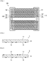
- Fig. 1 is a schematic sectional view illustrating an example of a film capacitor according to the present invention.
- the film capacitor 100 illustrated in Fig. 1 is a roll-type film capacitor and is constructed by rolling a metallized film 110 provided with a metal layer 20 disposed on the first surface 11 of a resin layer 10 and a metallized film 120 provided with a metal layer 40 disposed on the first surface 31 of a resin layer 30.
- an outer terminal electrode 51 electrically coupled to the metal layer 20 and an outer terminal electrode 52 electrically coupled to the metal layer 40 are provided.
- particles present on the surface of the resin layer are omitted from Fig. 1 .
- the metal layer 20 is formed so as to reach one side edge of the metallized film 110 but not to reach the other side edge. Meanwhile, the metal layer 40 is formed so as not to reach one side edge of the metallized film 120 but to reach the other side edge.
- the metal layer 20 and the metal layer 40 are composed of, for example, aluminum, zinc, or the like.
- the metallized film 110 and the metallized film 120 take on a stacked state by being rolled. As illustrated in Fig. 1 , the metallized film 110 and the metallized film 120 are shifted from each other in the width direction so that both the end portion which reaches the side edge of the metallized film 110 of the metal layer 20 and the end portion which reaches the side edge of the metallized film 120 of the metal layer 40 are exposed.
- rolling is performed so that the metallized film 110 is located outside the metallized film 120 and so that each of the metal layer 20 and the metal layer 40 of the metallized film 110 and the metallized film 120, respectively, faces inward.
- the outer terminal electrode 51 and the outer terminal electrode 52 are formed on the respective end surfaces of the thus obtained capacitor main body by, for example, thermally spraying zinc or the like.
- the outer terminal electrode 51 is in contact with the exposed end portion of the metal layer 20 so as to be electrically coupled to the metal layer 20.
- the outer terminal electrode 52 is in contact with the exposed end portion of the metal layer 40 so as to be electrically coupled to the metal layer 40.
- the film capacitor according to the present invention is made compact in the shape by being pressed into a flat shape having a cross-sectional shape like an ellipse or an oval.
- the film capacitor according to the present invention may include a circular-columnar roll shaft.
- the roll shaft is disposed on a center axis line of the metallized film in a rolled state and serves as a roll shaft when the metallized film is rolled.
- the film-capacitor film according to the present invention can be used as a film-capacitor film including a resin layer.
- the film-capacitor film according to the present invention may be used as the film-capacitor film for constituting both the metallized film 110 and the metallized film 120 or the film-capacitor film according to the present invention may be used for any one of them.
- the film-capacitor film according to the present invention is a film-capacitor film including a resin layer which has a first surface and a second surface and in which there are particles on at least one of the first surface and the second surface, wherein there are more particles in number on the surface of the resin layer than inside the resin layer.
- Fig. 2 is a schematic sectional view illustrating an example of the film-capacitor film according to the present invention.
- the film-capacitor film 1 is a dielectric resin film in which there are particles 13 on the second surface 12 of the resin layer 10. In the film-capacitor film 1, there is no particle on the first surface 11 of the resin layer 10. Meanwhile, there is no particle 13 inside the resin layer 10.
- the film-capacitor film there are particles on the surface of the resin layer. Particles being present on the surface of the resin layer provides the film surface with unevenness so that the friction coefficient of the film is reduced and the slipperiness of the film is improved. In this regard, particles for improving the slipperiness have to be present on the surface of the resin layer, and particles present inside the resin layer do not contribute to an improvement in the slipperiness. If there are particles inside the resin layer, the dielectric breakdown voltage is reduced, and, therefore the amount of the particles present inside the resin layer is made to be reduced. That is, it is intended that there are more particles in number on the surface of the resin layer than inside the resin layer.
- Particles present on the surface of the resin layer can be identified by observing the surface of the resin layer of the film-capacitor film by using a scanning electron microscope (SEM). Meanwhile, particles present inside the resin layer can be identified by increasing the acceleration voltage during observation of the surface of the resin layer of the film-capacitor film by using a scanning electron microscope (SEM). That is, a particle that is not observed at a low acceleration voltage but that is observed at an increased voltage is determined to be a particle present inside the resin layer.
- SEM scanning electron microscope
- the observation of the surface of the resin layer by using the scanning electron microscope (SEM) is performed while changing the acceleration voltage from a low voltage to a high voltage, the number of particles present on the surface of the resin layer and the number of particles present inside the resin layer are counted, and it is determined whether the number of particles present on the surface of the resin layer is greater than the number of particles present inside the resin layer.
- the number of particles present on the surface of the resin layer and the number of particles present inside the resin layer can be counted by changing the acceleration voltage within the range of 1 kV or more and 10 kV or less.
- particles present inside the resin layer do not contribute to an improvement in slipperiness and, in addition, cause a reduction in the dielectric breakdown voltage, no presence is preferable.
- Particles are preferably inorganic particles and more preferably silica particles.
- the average particle diameter of the particles is preferably 0.1 ⁇ m or more and 0.4 ⁇ m or less.
- the diameter of a particle present on the surface of the resin layer becomes greater in accordance with an increase in the acceleration voltage during observation of the surface of the resin layer by using the SEM (the maximum diameter of the embedded portion is observed).
- the area of a particle at the maximum size of the particle is converted to the equivalent circle diameter so as to determine the diameter of the particle.
- the average value of the diameters of particles in the field of view is taken as the average particle diameter of the particles.
- the average particle diameter of the particles denotes the average particle diameter of particles present on the surface of the resin layer.
- the number of the particles present on the surface of the resin layer being within the above-described range allows the effect of particles present on the surface of the resin layer to be sufficiently exerted. Meanwhile, even when the number of the particles present on the surface of the resin layer is increased beyond the above-described range, the effect of improving the slipperiness is not improved any more.
- the number of the particles present on the surface of the resin layer can be determined by measuring 10 fields of view (each field of view is 12.5 ⁇ m ⁇ 9.5 ⁇ m, and the total of 10 fields of view is 0.001188 mm 2 ) that are places randomly selected from the surface of the resin layer with an SEM at a magnification of 10,000 times and by counting the number of particles in the 10 fields of view observed at that time.
- the height of a particle protruding from the resin layer is preferably 0.005 ⁇ m or more and 0.1 ⁇ m or less.
- the height of a particle protruding from the surface of the resin layer being within the above-described range allows the effect of the particle present on the surface of the resin layer to be sufficiently exerted.
- the height of a particle protruding from the surface of the resin layer can be determined by observing the surface of the resin layer by using a scanning probe microscope (SPM) with a field of view of 2 ⁇ m ⁇ 2 ⁇ m.
- SPM scanning probe microscope
- the resin layer contains a resin having at least one of a urethane bond and a urea bond as a primary component.
- resins include urethane resins having a urethane bond and urea resins having a urea bond.
- resins having both a urethane bond and a urea bond may be included.
- the presence of a urethane bond and/or a urea bond can be identified by using a Fourier transform infrared spectrophotometer (FT-IR).
- FT-IR Fourier transform infrared spectrophotometer
- the resin layer may contain, for example, additives such as a silicone resin and uncured portions of starting materials such as a first organic material and a second organic material, described later, as components other than the primary component.
- the resin layer contains a curable resin as a primary component.
- the curable resin may be a thermosetting resin or may be a photo-curable resin.
- the resin layer may contain a thermoplastic resin.
- the thermosetting resin denotes a resin which can be cured by heat, and a curing method is not limited. Therefore, a resin that have cured by a method other than heat (for example, light, an electron beam, or the like) is also included in the thermosetting resin provided that the resin can be cured by heat.
- thermosetting resin a reaction may start due to the reactivity of just a material in accordance with the material, and the resin that is cured without the need for applying heat, light, or the like from the outside is included in the thermosetting resin.
- the curable resin is composed of the first organic material and the second organic material.
- examples include cured products obtained by a reaction between a hydroxy group (OH group) included in the first organic material and an isocyanate group (NCO group) included in the second organic material.
- the resin layer may contain an isocyanate group (NCO group).
- NCO group an isocyanate group
- the presence of an isocyanate group can be identified by using a Fourier transform infrared spectrophotometer (FT-IR).
- the first organic material is a polyol having a plurality of hydroxy groups (OH groups) in the molecule.
- the polyol include polyether polyols, polyester polyols, and polyvinyl acetoacetals.
- the first organic material at least two types of organic materials may be used in combination. Of the first organic materials, phenoxy resins belonging to polyether polyols are preferable.
- the second organic material is an isocyanate compound, an epoxy resin having an epoxy group, or a melamine resin, which has a plurality of functional groups in the molecule.
- the second organic material at least two types of organic materials may be used in combination.
- isocyanate compound examples include aromatic polyisocyanates such as diphenylmethane diisocyanate (MDI) and tolylene diisocyanate (TDI) and aliphatic polyisocyanates such as hexamethylene diisocyanate (HDI). Modified products of these polyisocyanates, for example, modified products containing carbodiimide, urethane, or the like may also be included. Of these, aromatic polyisocyanates are preferable, and MDI is more preferable.
- MDI diphenylmethane diisocyanate
- TDI tolylene diisocyanate
- HDI hexamethylene diisocyanate
- Modified products of these polyisocyanates for example, modified products containing carbodiimide, urethane, or the like may also be included. Of these, aromatic polyisocyanates are preferable, and MDI is more preferable.
- epoxy resin there is no particular limitation regarding the epoxy resin provided that the resin has an epoxy ring, and examples of the epoxy resin include bisphenol A type epoxy resins, biphenyl-skeleton epoxy resins, cyclopentadiene-skeleton epoxy resins, and naphthalene-skeleton epoxy resins.
- the melamine resin is an organic nitrogen compound having a triazine ring at the center of the structure and having 3 amino groups around the center, and examples thereof include alkylated melamine resins.
- modified products of melamine may be included.
- the resin layer may contain an additive for providing another function.
- adding a leveling agent enables the smoothness to be provided.
- the additive is a material having a functional group that reacts with a hydroxy group and/or an isocyanate group and that forms part of cross-linking structure of a cured product. Examples of such materials include resins having at least one functional group selected from a group consisting of an epoxy group, a silanol group, and a carboxy group.
- the thickness of the resin layer is preferably 1 ⁇ m or more and 5 ⁇ m or less.
- the thickness of the resin layer denotes a thickness measured at a position at which there is no particle on the surface.
- the thickness of the resin layer being 1 ⁇ m or more and 5 ⁇ m or less enables the number of defects such as cracks and the like generated during film formation to be reduced.
- the ratio of the particle diameter to the film thickness is preferably 0.13 or less.
- the ratio of the particle diameter to the film thickness is preferably 0.04 or more.
- the particle diameter is the average particle diameter of particles. in the case in which at least two types of particles are used, the ratio of the particle diameter to the film thickness is calculated by using the particle diameter of a larger particle.
- Fig. 3 is a schematic sectional view illustrating another example of the film-capacitor film according to the present invention.
- the film-capacitor film 2 is a dielectric resin film in which there are particles 13 on the second surface 12 of the resin layer 10, and there are particles 13 on also the first surface 11 of the resin layer 10. Meanwhile, there is no particle 13 inside the resin layer 10.
- Particles being present on the first surface and the second surface of the resin layer enables the slipperiness of the film to be further improved.
- the film-capacitor film of this form there are more particles in number on both the first surface and the second surface of the resin layer than inside the resin layer.
- Such a film-capacitor film can also exert the effect of the film-capacitor film according to the present invention.
- the dielectric breakdown voltage of the film-capacitor film according to the present invention is preferably 300 V/ ⁇ m or more.
- an aluminum thin film serving as an electrode is disposed on the first surface and the second surface of the film by using a vacuum vapor deposition device, and thereafter a voltage is applied to the film in an atmosphere at 125°C. The voltage is increased until a hole is made in the film, and the voltage at which a hole is made in the film is taken as the dielectric breakdown voltage.
- the dielectric breakdown voltage is measured at 16 points, and an average value thereof is determined.
- the film-capacitor film according to the present invention has a friction coefficient suitable for smooth sliding of films stacked on each other.
- the first surface of one film and the second surface of the other film are stacked, and the friction coefficient is measured.
- the second surface (surface on which particles are present) of one film and the first surface (surface on which no particle is present) of the other film are stacked.
- the second surface (surface on which particles are present) of one film and the first surface (surface on which particles are present) of the other film are stacked.
- the measurement of the friction coefficient is performed in conformity with JIS K 7125, and the friction coefficient is preferably 1.0 or less so as to be suitable for smooth sliding of films stacked on each other.
- the friction coefficient either a static friction coefficient or a dynamic friction coefficient may be used.
- the film-capacitor films illustrated in Fig. 2 and Fig. 3 be made into a metallized film by the first surface of the resin layer being provided with the metal layer and be used for producing a film capacitor, as described later.
- the metal layer may be disposed on the surface on which particles are present or may be disposed on the surface on which no particle is present.
- the film-capacitor film according to the present invention can be made into a metallized film by providing a metal layer on the first surface of the resin layer.
- Fig. 4(a) and Fig. 4(b) are schematic sectional views illustrating examples of a metallized film in which a metal layer is disposed on the film-capacitor film according to the present invention.
- a metal layer 20 is disposed on the first surface 11 of the resin layer 10, and there are particles 13 on the second surface 12 of the resin layer 10. That is, in the resin layer, the metal layer is disposed on the surface on which there is no particle.
- a metal layer 20 is disposed on the first surface 11 of the resin layer 10, and there are particles 13 on the second surface 12 of the resin layer 10, and, in addition, there are particles 13 on also the first surface 11 of the resin layer 10. That is, in the resin layer, the metal layer is disposed on the surface on which there are particles. In this case, at least some of the surfaces of the particles 13 present on the first surface 11 of the resin layer 10 may be exposed at the metal layer 20.
- the effect of improving the slipperiness is further favorably exerted.
- the entire surfaces of the particles may be covered with the metal layer.
- the effect of improving the slipperiness is somewhat reduced since the unevenness of the film surface formed by particles is lessened.
- the effect of improving the slipperiness is exerted even when the entire surfaces of the particles are covered with the metal layer.
- the number of the particles exposed at the metal layer can be determined by measuring 10 fields of view (each field of view is 12.5 ⁇ m ⁇ 9.5 ⁇ m, and the total of 10 fields of view is 0.001188 mm 2 ) that are places randomly selected from the surface of the metallized film with an SEM at a magnification of 10,000 times and by counting the number of particles in the 10 fields of view observed at that time.
- Examples of the metal layer include aluminum, zinc, and the like.
- the material constituting the metal layer being aluminum or zinc facilitates maintenance of favorable bondability to an outer terminal electrode.
- the thickness of the metal layer is preferably 5 nm or more and 50 nm or less.
- the thickness of the metal layer is determined in consideration of the resistance value of the metal layer.
- the thickness of the metal layer is determined so that the surface resistance of the metal layer becomes 20 ⁇ / ⁇ or less. If the thickness of the metal layer is excessively small, the conduction of the metal layer portion may become open.
- the metal layer is provided with a fuse portion.
- the fuse portion denotes a portion of the metal layer serving as a counter electrode, the portion connecting electrode portions divided into a plurality of parts to each other.
- the pattern of the metal layer having the fuse portion For example, electrode patterns disclosed in Japanese Unexamined Patent Application Publication No. 2004-363431 , Japanese Unexamined Patent Application Publication No. 5-251266 , and the like may be used.
- the method for manufacturing the film-capacitor film according to the present invention includes forming a resin layer by coating a base material film with a resin solution.
- a film in which particles are attached to a resin-solution-coating surface is used.
- the particles that have been attached to the base material film are attached to the applied resin solution.
- the particles are transferred from the base material film to the surface of the resin layer by peeling the resin layer off the base material film.
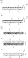
- Fig. 5(a), Fig. 5(b), and Fig. 5(c) are schematic step diagrams illustrating an example of a method for manufacturing the film-capacitor film according to the present invention.
- a base material film 70 is prepared.
- the base material film 70 is a film including particles 13 in the inside and on the surface, and particles 13 are attached to a resin-solution-coating surface 71.
- the resin-solution-coating surface 71 of the base material film 70 is coated with the resin solution, and after the resin solution is applied, the resin is subjected to curing treatment, drying treatment, and the like, as the situation demands, so as to form the resin layer 10. Subsequently, as illustrated in Fig. 5(c) , the particles 13 are transferred from the base material film 70 to the second surface 12 of the resin layer 10 by peeling the resin layer 10 off the base material film 70. In this manner, the film-capacitor film 1 is obtained.
- the base material film is a polypropylene film.
- the base material film it is preferable that particles be kneaded into the film, and particles be attached to the film surface.
- a resin solution used for forming the film-capacitor film a resin solution in which a resin serving as a raw material or a precursor of the resin is dispersed in a solvent can be used.
- the solvent methyl ethyl ketone, tetrahydrofuran, ethyl acetate, or the like
- the resin solution may be present as a residue in the resin layer.
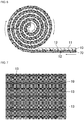
- Fig. 6 is a schematic step diagram illustrating an example of the state of rolling the film after coating.
- Fig. 6 illustrates the state of rolling the film after coating where the resin layer 10 is formed by coating the base material film 70 with a resin solution. The rolling direction is indicated by arrows in Fig. 6 . As illustrated in Fig.
- the rolled film after coating is spread by being rotated in the direction opposite to the rolling direction so that particles 13 are transferred to the first surface 11 of the resin layer 10.
- the resin layer 10 is peeled off the base material film 70 so as to transfer the particles 13 to the second surface 12 of the resin layer 10.
- the film-capacitor film in which there are particles on the first surface and the second surface of the resin layer is obtained.
- a method for manufacturing a film capacitor according to the present invention will be described.
- a metallized film is obtained by disposing a metal layer on the first surface of the resin layer of the film-capacitor film according to the present invention.
- Examples of the method for disposing the metal layer on the first surface of the resin layer of the film-capacitor film include a vapor deposition method.
- the resin layer 10 is formed on the base material film 70.
- a metal layer 20 can be disposed on the resin layer 10 by subjecting the surface of the resin layer 10 opposite to the base material film 70 to vapor deposition or the like.
- the surface provided with the metal layer as described above serves as the first surface of the resin layer, and the base-material-film-side surface to which particles are attached serves as the second surface.
- the metallized film obtained by peeling the base material film after the above-described step is a metallized film 111 illustrated in Fig. 4(a) .
- the resin layer 10 is formed on the base material film 70, and particles 13 are attached to the surface of the resin layer 10 opposite to the base material film 70.
- the metal layer 20 can be disposed on the surface of the resin layer 10 to which particles 13 are attached by subjecting the surface of the resin layer 10 opposite to the base material film 70 to vapor deposition or the like.
- the surface provided with the metal layer as described above serves as the first surface of the resin layer, and the base-material-film-side surface to which particles are attached serves as the second surface of the resin layer.
- the metallized film obtained by peeling the base material film after the above-described step is a metallized film 112 illustrated in Fig. 4(b) .
- the thickness of the metal layer is adjusted so that the surface resistance of the metal layer becomes 20 ⁇ / ⁇ or less. At this time, at least some of the surfaces of the particles may be exposed at the metal layer.
- the metal layer may be formed on the resin layer after the resin layer is peeled off the base material film.
- a multilayer body is obtained by stacking two such metallized films in the state of being shifted a predetermined distance from each other in the width direction and by performing rolling. As the situation demands, the multilayer body may be sandwiched in the direction perpendicular to the width direction and may be pressed into the shape of an elliptical cylinder. Subsequently, an outer terminal electrode is formed on the end surface of the multilayer body so as to obtain a film capacitor as illustrated in Fig. 1 . Examples of the method for forming the outer terminal electrode on the end surface of the multilayer body include thermal spraying.
- a resin solution was prepared by dissolving a phenoxy resin and a modified product of diphenylmethane diisocyanate (MDI) into an organic solvent and further adding a silicone-containing surface additive BYK-370 (produced by BYK Japan KK) .
- MDI diphenylmethane diisocyanate
- BYK-370 silicone-containing surface additive
- the resulting resin solution was applied to a polypropylene film (TORAYFAN: produced by Toray Industries, Ltd., thickness of 12 ⁇ m) in which silica particles having an average particle diameter of 0.1 ⁇ m (particle diameter distribution of 0.04 ⁇ m to 0.3 ⁇ m) and silica particles having an average particle diameter of 0.4 ⁇ m (particle diameter distribution of 0.2 ⁇ m.
- the number of the particles on the film surface was determined by measuring 10 fields of view (each field of view was 12.5 ⁇ m ⁇ 9.5 ⁇ m, and the total of 10 fields of view was 0.001188 mm 2 ) that were places randomly selected from the second-surface-side surface of the resin layer (film-capacitor film) with an SEM at a magnification of 10,000 times and by counting the number of particles in the 10 fields of view observed at that time.
- the dielectric breakdown voltage of the film was measured by disposing an aluminum thin film serving as an electrode on the first surface and the second surface of the film by using a vacuum vapor deposition device and thereafter applying a voltage to the film in an atmosphere at 125°C.
- the voltage was increased until a hole was made in the film, and the voltage at which a hole was made in the film was taken as the dielectric breakdown voltage.
- the dielectric breakdown voltage of the film was measured at 16 points, and an average value thereof was determined.
- the measurement of the friction coefficient was performed in conformity with JIS K 7125, and the dynamic friction coefficient and the static friction coefficient were determined.
- the friction coefficient was measured while the second surface (polypropylene-film-side surface) and the first surface (surface opposite to the second surface) of the resulting film were stacked.
- a film (film-capacitor film) having a thickness of about 2.3 ⁇ m was produced in the same manner as in Example 1 except that the amount of the resin solution applied was changed. Silica particles were partly buried under the second surface and the first surface of the resulting film. The number of particles on the film surface, the dielectric breakdown voltage of the film, and the friction coefficient between the films were measured. The results are described in Table 1.
- a film (film-capacitor film) having a thickness of about 2.3 ⁇ m was produced in the same manner as in Example 1 except that a polypropylene film (TORAYFAN: produced by Toray Industries, Ltd., thickness of 12 ⁇ m) in which silica particles having an average particle diameter of 0.1 ⁇ m (particle diameter distribution of 0.04 ⁇ m to 0.3 ⁇ m) were attached to the surface was used as the film to be coated with the resin solution. Silica particles were partly buried under the second surface and the first surface of the resulting film. The number of particles on the film surface, the dielectric breakdown voltage of the film, and the friction coefficient between the films were measured. The results are described in Table 1.
- a film (film-capacitor film) having a thickness of about 1.0 ⁇ m was produced in the same manner as in Example 3 except that the amount of the resin solution applied was changed. Silica particles were partly buried under the second surface and the first surface of the resulting film. The number of particles on the film surface, the dielectric breakdown voltage of the film, and the friction coefficient between the films were measured. The results are described in Table 1.
- a resin solution was prepared by dissolving a thermoplastic polyarylate (UNIFINER produced by UNITIKA LTD.) into an organic solvent.
- the resulting resin solution was applied to a polypropylene film (TORAYFAN: produced by Toray Industries, Ltd., thickness of 12 ⁇ m) in which silica particles having an average particle diameter of 0.1 ⁇ m (particle diameter distribution of 0.04 ⁇ m to 0.3 ⁇ m) and silica particles having an average particle diameter of 0.4 ⁇ m (particle diameter distribution of 0.2 ⁇ m to 0.6 ⁇ m) were attached to the surface, the solvent was dried, and the film after coating was rolled as illustrated in Fig. 6 .
- the rolled film after coating was spread by being rotated in the direction opposite to the rolling direction and was peeled off the polypropylene film so as to produce a film (film-capacitor film) having a thickness of about 3.0 ⁇ m.
- Silica particles were partly buried under the second surface (polypropylene-film-side surface) and the first surface (surface opposite to the polypropylene film) of the resulting film. The number of particles on the second-surface-side film surface, the dielectric breakdown voltage of the film, and the friction coefficient between the films were measured. The results are described in Table 1.
- Silica particles having an average particle diameter of 0.2 ⁇ m and a silane coupling agent were placed into a solvent in which toluene and ethanol was mixed at a weight ratio of 1:1, and agitation was performed for 8 hours in a ball mill so as to produce a silica particle dispersion liquid in which silica particles surface-treated with the silane coupling agent were dispersed. According to measurement of the particle diameter distribution of particles in the resulting silica particle dispersion liquid, the average particle diameter was 0.4 ⁇ m.
- a phenoxy resin and an MDI modified product were dissolved into an organic solvent and were mixed, and a silicone-containing surface additive BYK-370 (produced by BYK Japan KK) was further added.
- the resin solution was prepared by adding the silica particle dispersion liquid produced as described above so that the ratio of the particles relative to a solid content weight of the phenoxy resin and the MDI modified product became 1% by weight.
- the resulting resin solution was applied to a smooth PET film provided with a mold-release layer on the surface, and the solvent was dried.
- a film film-capacitor film having a thickness of about 3.0 ⁇ m was produced by being peeled off the PET film. The number of particles on the film surface, the dielectric breakdown voltage of the film, and the friction coefficient between the films were measured. The results are described in Table 1.
- a phenoxy resin and an MDI modified product were dissolved into an organic solvent and were mixed, and a surface additive was further added. Thereafter, the resin solution was prepared by adding a dispersion liquid of silica having a particle diameter of 0.01 to 0.015 ⁇ m (ORGANOSILICASOL MEK-ST produced by Nissan Chemical Industries, Ltd.) so that the ratio of the particles relative to a solid content weight of the phenoxy resin and the MDI modified product became 1% by weight. The resulting resin solution was applied to a smooth PET film provided with a mold-release layer on the surface, and the solvent was dried.
- a dispersion liquid of silica having a particle diameter of 0.01 to 0.015 ⁇ m ORGANOSILICASOL MEK-ST produced by Nissan Chemical Industries, Ltd.
- a film (film-capacitor film) having a thickness of about 3.0 ⁇ m was produced by being peeled off the PET film. The number of particles on the film surface, the dielectric breakdown voltage of the film, and the friction coefficient between the films were measured. The results are described in Table 1.
- a resin solution was prepared by dissolving the thermoplastic polyarylate (UNIFINER produced by UNITIKA LTD.) into an organic solvent and adding the silica particle dispersion liquid produced in the same manner as in Comparative example 1 so that the ratio of the particles relative to a solid content weight of the polyarylate became 1% by weight.
- the resulting resin solution was applied to a smooth PET film provided with a mold-release layer on the surface. After the solvent was dried, a film (film-capacitor film) having a thickness of about 3.0 ⁇ m. was produced by being peeled off the PET film. The number of particles on the film surface, the dielectric breakdown voltage of the film, and the friction coefficient between the films were measured. The results are described in Table 1.
- Fig. 7 is an SEM image of the surface (second surface) of the film-capacitor film produced in Example 1. It is clear that there are particles 13 on the surface of the resin layer 10.
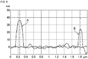
- Fig. 8 is a graph illustrating the results of observing the surface (second surface) of the resin layer with respect to the film-capacitor film produced in Example 1 by using a scanning probe microscope (SPM). The measurement results at two places are illustrated in combination, and it is clear that the height of the particle protruding from the resin layer is about 36 nm (0.036 ⁇ m) on the left side (indicated by arrow A) and is about 22 nm (0.022 ⁇ m) on the right side (indicated by arrow B).
- SPM scanning probe microscope
- silica particles having a height of 20 to 40 nm protrude from the surface of the resin layer, and presence of silica particles on the surface of the resin layer was clarified.
- silica particles were observed even after the metal layer was formed on the surface of the resin layer on which silica particles were present. It is considered that, since the thickness of the metal layer was small, the silica particles penetrated through the electrode or an electrode did not attached around the silica particles. According to this result, it is conjectured that the particles were observed on the electrode during the measurement of the dielectric breakdown voltage.
- Example 1 the dielectric breakdown voltage of Comparative example 1 was low since there were silica particles inside the resin layer.
- Comparative example 2 since the size of silica particle was excessively small, all silica particles were embedded inside the resin layer, there was no silica on the surface of the resin layer, and unevenness could not be formed. Consequently, slipperiness was poor when the film-capacitor films were stacked on each other. In this state, it was difficult to work the film-capacitor film into a capacitor.
- Example 1 According to comparisons between Example 1 and Example 2, it was clarified that the dielectric breakdown voltage was large when the ratio of the particle diameter to the film thickness was small. Therefore, in Examples 3 and 4, the particle diameter of the particles was reduced, and the ratio of the particle diameter of the raw material particles to the film thickness was reduced. As a result, the dielectric breakdown voltage was further increased. It is conjectured that, in the case in which there is no particle inside the resin layer, the ratio of the particle diameter of the raw material particles to the film thickness is in correlation with the dielectric breakdown voltage of the film.
- Example 5 According to comparisons between Example 5 and Comparative example 3 in which the thermoplastic resin was used as the resin, it was clarified that the relationship between presence or absence of particles inside the resin layer and the dielectric breakdown voltage also applied to the case in which the resin was the thermoplastic resin.
Landscapes
- Engineering & Computer Science (AREA)
- Power Engineering (AREA)
- Manufacturing & Machinery (AREA)
- Microelectronics & Electronic Packaging (AREA)
- Chemical & Material Sciences (AREA)
- Inorganic Chemistry (AREA)
- Mechanical Engineering (AREA)
- Fixed Capacitors And Capacitor Manufacturing Machines (AREA)
- Laminated Bodies (AREA)
Abstract
Description
- The present invention relates to a film capacitor, a film-capacitor film, and a method for manufacturing a film-capacitor film.
- A film capacitor having a structure in which a flexible resin film is used as a dielectric and a first counter electrode and a second counter electrode are arranged opposite to each other with the resin film interposed therebetween is one of capacitors. Such a film capacitor is produced by, for example, rolling a resin film provided with the first counter electrode and a resin film provided with the second counter electrode (refer to, for example, Patent Document 1).
- Patent Document 1: International Publication No.
2013/069485 - A self-healing function of a film capacitor is performed by a fuse portion disposed in the film capacitor being cut due to an occurrence of short circuit. If the adhesiveness between the films of the fuse portion is excessively high, since a vapor-deposition electrode is not readily scattered, the fuse portion based on a short current during dielectric breakdown is not limited to operating and the self-healing function is not limited to being sufficiently performed.
In this regard, a capacitor with high safety can be provided by highly roughening the surfaces of the films so as to reduce adhesiveness between the films. - Meanwhile, if the surface of the film is smooth, since the friction coefficient increases (slipperiness of the film is poor), the handleability of the film is poor, and degradation in the operability of the film is caused during transportation, taking up, and the like of the film.
- To provide slipperiness to the film, a technique to provide unevenness to the film surface by attaching particles to the film is performed.
According to this technique, the slipperiness of the film is improved, but there is a problem of a reduction in dielectric breakdown voltage since particles serving as impurities are contained inside the film. - In accordance with such circumstances, the compatibility between an improvement in the slipperiness of a film-capacitor film and a high dielectric breakdown voltage has been desired.
- The present invention was realized to address the above-described problems, and it is an object to provide a film capacitor including a film-capacitor film having high slipperiness and a high dielectric breakdown voltage. In addition, it is an object to provide a film-capacitor film for producing the film capacitor and to provide a method for manufacturing the film-capacitor film.
- A film capacitor according to the present invention includes a resin layer which has a first surface and a second surface and in which there are particles on at least one of the first surface and the second surface and a metal layer disposed on the first surface of the resin layer, wherein there are more particles in number on the surface of the resin layer than inside the resin layer.
- A film-capacitor film according to the present invention includes a resin layer which has a first surface and a second surface and in which there are particles on at least one of the first surface and the second surface, wherein there are more particles in number on the surface of the resin layer than inside the resin layer.
- A method for manufacturing a film-capacitor film according to the present invention includes forming a resin layer by coating a base material film with a resin solution, wherein particles are attached to a resin-solution-coating surface of the base material film, and the particles are transferred from the base material film to the surface of the resin layer by peeling the resin layer off the base material film.
- According to the present invention, a film capacitor including a film-capacitor film having high slipperiness and a high dielectric breakdown voltage can be provided.
-
- [
Fig. 1] Fig. 1 is a schematic sectional view illustrating an example of a film capacitor according to the present invention. - [
Fig. 2] Fig. 2 is a schematic sectional view illustrating an example of a film-capacitor film according to the present invention. - [
Fig. 3] Fig. 3 is a schematic sectional view illustrating another example of the film-capacitor film according to the present invention. - [
Fig. 4] Fig. 4(a) and Fig. 4(b) are schematic sectional views illustrating examples of a metallized film in which a metal layer is disposed on a film-capacitor film according to the present invention. - [
Fig. 5] Fig. 5(a), Fig. 5(b), and Fig. 5(c) are schematic step diagrams illustrating an example of a method for manufacturing a film-capacitor film according to the present invention. - [
Fig. 6] Fig. 6 is a schematic step diagram illustrating an example of the state of rolling a film after coating. - [
Fig. 7] Fig. 7 is an SEM image of the surface of a film-capacitor film produced in Example 1. - [
Fig. 8] Fig. 8 is a graph illustrating the results of observing the surface of a resin layer with respect to the film-capacitor film produced in Example 1 by using a scanning probe microscope (SPM). - A film capacitor, a film-capacitor film for producing the film capacitor, and a method for manufacturing the film-capacitor film according to the present invention will be described below.
However, The present invention is not limited to the following configurations and the configurations can be appropriately modified and applied within the bounds of not changing the spirit of the present invention. Combination of at least two independent desirable configurations of the present invention described below are also included in the present invention. - A roll-type film capacitor will be described as an embodiment of the film capacitor according to the present invention.
-
Fig. 1 is a schematic sectional view illustrating an example of a film capacitor according to the present invention. Thefilm capacitor 100 illustrated inFig. 1 is a roll-type film capacitor and is constructed by rolling ametallized film 110 provided with ametal layer 20 disposed on thefirst surface 11 of aresin layer 10 and ametallized film 120 provided with ametal layer 40 disposed on thefirst surface 31 of aresin layer 30.
In addition, anouter terminal electrode 51 electrically coupled to themetal layer 20 and anouter terminal electrode 52 electrically coupled to themetal layer 40 are provided.
In this regard, particles present on the surface of the resin layer are omitted fromFig. 1 . - The
metal layer 20 is formed so as to reach one side edge of themetallized film 110 but not to reach the other side edge. Meanwhile, themetal layer 40 is formed so as not to reach one side edge of themetallized film 120 but to reach the other side edge. Themetal layer 20 and themetal layer 40 are composed of, for example, aluminum, zinc, or the like. - The
metallized film 110 and themetallized film 120 take on a stacked state by being rolled. As illustrated inFig. 1 , themetallized film 110 and themetallized film 120 are shifted from each other in the width direction so that both the end portion which reaches the side edge of themetallized film 110 of themetal layer 20 and the end portion which reaches the side edge of themetallized film 120 of themetal layer 40 are exposed. - In the
film capacitor 100 illustrated inFig. 1 , rolling is performed so that themetallized film 110 is located outside themetallized film 120 and so that each of themetal layer 20 and themetal layer 40 of themetallized film 110 and themetallized film 120, respectively, faces inward. - The
outer terminal electrode 51 and theouter terminal electrode 52 are formed on the respective end surfaces of the thus obtained capacitor main body by, for example, thermally spraying zinc or the like. Theouter terminal electrode 51 is in contact with the exposed end portion of themetal layer 20 so as to be electrically coupled to themetal layer 20. Meanwhile, theouter terminal electrode 52 is in contact with the exposed end portion of themetal layer 40 so as to be electrically coupled to themetal layer 40. - Preferably, the film capacitor according to the present invention is made compact in the shape by being pressed into a flat shape having a cross-sectional shape like an ellipse or an oval. In this regard, the film capacitor according to the present invention may include a circular-columnar roll shaft. The roll shaft is disposed on a center axis line of the metallized film in a rolled state and serves as a roll shaft when the metallized film is rolled.
- In production of the film capacitor, the film-capacitor film according to the present invention can be used as a film-capacitor film including a resin layer. In this regard, the film-capacitor film according to the present invention may be used as the film-capacitor film for constituting both the
metallized film 110 and themetallized film 120 or the film-capacitor film according to the present invention may be used for any one of them. - The film-capacitor film according to the present invention is a film-capacitor film including a resin layer which has a first surface and a second surface and in which there are particles on at least one of the first surface and the second surface, wherein there are more particles in number on the surface of the resin layer than inside the resin layer.
-
Fig. 2 is a schematic sectional view illustrating an example of the film-capacitor film according to the present invention.
The film-capacitor film 1 is a dielectric resin film in which there areparticles 13 on thesecond surface 12 of theresin layer 10. In the film-capacitor film 1, there is no particle on thefirst surface 11 of theresin layer 10. Meanwhile, there is noparticle 13 inside theresin layer 10. - In the film-capacitor film according to the present invention, there are particles on the surface of the resin layer.
Particles being present on the surface of the resin layer provides the film surface with unevenness so that the friction coefficient of the film is reduced and the slipperiness of the film is improved.
In this regard, particles for improving the slipperiness have to be present on the surface of the resin layer, and particles present inside the resin layer do not contribute to an improvement in the slipperiness.
If there are particles inside the resin layer, the dielectric breakdown voltage is reduced, and, therefore the amount of the particles present inside the resin layer is made to be reduced.
That is, it is intended that there are more particles in number on the surface of the resin layer than inside the resin layer. - Particles present on the surface of the resin layer can be identified by observing the surface of the resin layer of the film-capacitor film by using a scanning electron microscope (SEM).
Meanwhile, particles present inside the resin layer can be identified by increasing the acceleration voltage during observation of the surface of the resin layer of the film-capacitor film by using a scanning electron microscope (SEM). That is, a particle that is not observed at a low acceleration voltage but that is observed at an increased voltage is determined to be a particle present inside the resin layer.
The observation of the surface of the resin layer by using the scanning electron microscope (SEM) is performed while changing the acceleration voltage from a low voltage to a high voltage, the number of particles present on the surface of the resin layer and the number of particles present inside the resin layer are counted, and it is determined whether the number of particles present on the surface of the resin layer is greater than the number of particles present inside the resin layer.
In this regard, the number of particles present on the surface of the resin layer and the number of particles present inside the resin layer can be counted by changing the acceleration voltage within the range of 1 kV or more and 10 kV or less. - Meanwhile, it is preferable that there be no particle inside the resin layer. Since particles present inside the resin layer do not contribute to an improvement in slipperiness and, in addition, cause a reduction in the dielectric breakdown voltage, no presence is preferable.
- Particles are preferably inorganic particles and more preferably silica particles.
The average particle diameter of the particles is preferably 0.1 µm or more and 0.4 µm or less.
The diameter of a particle present on the surface of the resin layer becomes greater in accordance with an increase in the acceleration voltage during observation of the surface of the resin layer by using the SEM (the maximum diameter of the embedded portion is observed). The area of a particle at the maximum size of the particle is converted to the equivalent circle diameter so as to determine the diameter of the particle. The average value of the diameters of particles in the field of view is taken as the average particle diameter of the particles.
Herein, the average particle diameter of the particles denotes the average particle diameter of particles present on the surface of the resin layer. - In addition, it is preferable that 5 or more and 16 or less particles be present per 0.001188 mm2 of the surface of the resin layer.
The number of the particles present on the surface of the resin layer being within the above-described range allows the effect of particles present on the surface of the resin layer to be sufficiently exerted. Meanwhile, even when the number of the particles present on the surface of the resin layer is increased beyond the above-described range, the effect of improving the slipperiness is not improved any more.
The number of the particles present on the surface of the resin layer can be determined by measuring 10 fields of view (each field of view is 12.5 µm × 9.5 µm, and the total of 10 fields of view is 0.001188 mm2) that are places randomly selected from the surface of the resin layer with an SEM at a magnification of 10,000 times and by counting the number of particles in the 10 fields of view observed at that time. - Meanwhile, the height of a particle protruding from the resin layer is preferably 0.005 µm or more and 0.1 µm or less.
The height of a particle protruding from the surface of the resin layer being within the above-described range allows the effect of the particle present on the surface of the resin layer to be sufficiently exerted.
The height of a particle protruding from the surface of the resin layer can be determined by observing the surface of the resin layer by using a scanning probe microscope (SPM) with a field of view of 2 µm × 2 µm. - Preferably, the resin layer contains a resin having at least one of a urethane bond and a urea bond as a primary component. Examples of such resins include urethane resins having a urethane bond and urea resins having a urea bond. In addition, resins having both a urethane bond and a urea bond may be included.
In this regard, the presence of a urethane bond and/or a urea bond can be identified by using a Fourier transform infrared spectrophotometer (FT-IR). - In the present specification, "primary component" denotes a component having a maximum proportion (% by weight) and preferably denotes a component having a proportion of more than 50% by weight. Therefore, the resin layer may contain, for example, additives such as a silicone resin and uncured portions of starting materials such as a first organic material and a second organic material, described later, as components other than the primary component.
- Preferably, the resin layer contains a curable resin as a primary component. The curable resin may be a thermosetting resin or may be a photo-curable resin. In this regard, the resin layer may contain a thermoplastic resin.
In the case in which the resin layer is a thermoplastic resin, a polyarylate resin and the like can be used. In the present specification, the thermosetting resin denotes a resin which can be cured by heat, and a curing method is not limited. Therefore, a resin that have cured by a method other than heat (for example, light, an electron beam, or the like) is also included in the thermosetting resin provided that the resin can be cured by heat. Meanwhile, a reaction may start due to the reactivity of just a material in accordance with the material, and the resin that is cured without the need for applying heat, light, or the like from the outside is included in the thermosetting resin. The same applies to the photo-curable resin and there is no limitation regarding the curing method. - Preferably, the curable resin is composed of the first organic material and the second organic material. Examples include cured products obtained by a reaction between a hydroxy group (OH group) included in the first organic material and an isocyanate group (NCO group) included in the second organic material.
- In the case in which a cured product is obtained by the above-described reaction, uncured portions of start materials may remain in the resin layer. For example, the resin layer may contain an isocyanate group (NCO group). In this regard, the presence of an isocyanate group can be identified by using a Fourier transform infrared spectrophotometer (FT-IR).
- Preferably, the first organic material is a polyol having a plurality of hydroxy groups (OH groups) in the molecule. Example of the polyol include polyether polyols, polyester polyols, and polyvinyl acetoacetals. Regarding the first organic material, at least two types of organic materials may be used in combination. Of the first organic materials, phenoxy resins belonging to polyether polyols are preferable.
- Preferably, the second organic material is an isocyanate compound, an epoxy resin having an epoxy group, or a melamine resin, which has a plurality of functional groups in the molecule. Regarding the second organic material, at least two types of organic materials may be used in combination.
- Examples of the isocyanate compound include aromatic polyisocyanates such as diphenylmethane diisocyanate (MDI) and tolylene diisocyanate (TDI) and aliphatic polyisocyanates such as hexamethylene diisocyanate (HDI). Modified products of these polyisocyanates, for example, modified products containing carbodiimide, urethane, or the like may also be included. Of these, aromatic polyisocyanates are preferable, and MDI is more preferable.
- There is no particular limitation regarding the epoxy resin provided that the resin has an epoxy ring, and examples of the epoxy resin include bisphenol A type epoxy resins, biphenyl-skeleton epoxy resins, cyclopentadiene-skeleton epoxy resins, and naphthalene-skeleton epoxy resins.
- There is no particular limitation regarding the melamine resin provided that the resin is an organic nitrogen compound having a triazine ring at the center of the structure and having 3 amino groups around the center, and examples thereof include alkylated melamine resins. In addition, modified products of melamine may be included.
- The resin layer may contain an additive for providing another function. For example, adding a leveling agent enables the smoothness to be provided. More preferably, the additive is a material having a functional group that reacts with a hydroxy group and/or an isocyanate group and that forms part of cross-linking structure of a cured product. Examples of such materials include resins having at least one functional group selected from a group consisting of an epoxy group, a silanol group, and a carboxy group.
- There is no particular limitation regarding the thickness of the resin layer, and the thickness is preferably 1 µm or more and 5 µm or less.
Herein, the thickness of the resin layer denotes a thickness measured at a position at which there is no particle on the surface.
The thickness of the resin layer being 1 µm or more and 5 µm or less enables the number of defects such as cracks and the like generated during film formation to be reduced. - In the case in which there is no particle inside the resin layer, regarding the relationship between the thickness of the resin layer and the particle diameter of the particle, a reduction in the ratio of the particle diameter to the film thickness (particle diameter/film thickness) is preferable because of an increase in the dielectric breakdown voltage.
In the case in which there is no particle inside the resin layer, the ratio of the particle diameter to the film thickness (particle diameter [µm]/film thickness [µm]) is preferably 0.13 or less.
In this regard, in the case in which there is no particle inside the resin layer, the ratio of the particle diameter to the film thickness (particle diameter [µm]/film thickness [µm]) is preferably 0.04 or more.
Herein, the particle diameter is the average particle diameter of particles. in the case in which at least two types of particles are used, the ratio of the particle diameter to the film thickness is calculated by using the particle diameter of a larger particle. -
Fig. 3 is a schematic sectional view illustrating another example of the film-capacitor film according to the present invention.
The film-capacitor film 2 is a dielectric resin film in which there areparticles 13 on thesecond surface 12 of theresin layer 10, and there areparticles 13 on also thefirst surface 11 of theresin layer 10.
Meanwhile, there is noparticle 13 inside theresin layer 10. - Particles being present on the first surface and the second surface of the resin layer enables the slipperiness of the film to be further improved.
In addition, in the film-capacitor film of this form, there are more particles in number on both the first surface and the second surface of the resin layer than inside the resin layer. Such a film-capacitor film can also exert the effect of the film-capacitor film according to the present invention. - The dielectric breakdown voltage of the film-capacitor film according to the present invention is preferably 300 V/µm or more.
In the case in which the dielectric breakdown voltage of a film is measured, an aluminum thin film serving as an electrode is disposed on the first surface and the second surface of the film by using a vacuum vapor deposition device, and thereafter a voltage is applied to the film in an atmosphere at 125°C.
The voltage is increased until a hole is made in the film, and the voltage at which a hole is made in the film is taken as the dielectric breakdown voltage. The dielectric breakdown voltage is measured at 16 points, and an average value thereof is determined. - Preferably, the film-capacitor film according to the present invention has a friction coefficient suitable for smooth sliding of films stacked on each other.
In the case in which two films are stacked, the first surface of one film and the second surface of the other film are stacked, and the friction coefficient is measured. In the case in which there are particles on the second surface of the resin layer and there is no particle on the first surface, the second surface (surface on which particles are present) of one film and the first surface (surface on which no particle is present) of the other film are stacked. In the case in which there are particles on both the first surface and the second surface of the resin layer, the second surface (surface on which particles are present) of one film and the first surface (surface on which particles are present) of the other film are stacked.
The measurement of the friction coefficient is performed in conformity with JIS K 7125, and the friction coefficient is preferably 1.0 or less so as to be suitable for smooth sliding of films stacked on each other. Regarding the friction coefficient, either a static friction coefficient or a dynamic friction coefficient may be used. - It is preferable that the film-capacitor films illustrated in
Fig. 2 and Fig. 3 be made into a metallized film by the first surface of the resin layer being provided with the metal layer and be used for producing a film capacitor, as described later.
The metal layer may be disposed on the surface on which particles are present or may be disposed on the surface on which no particle is present. - The film-capacitor film according to the present invention can be made into a metallized film by providing a metal layer on the first surface of the resin layer.
Fig. 4(a) and Fig. 4(b) are schematic sectional views illustrating examples of a metallized film in which a metal layer is disposed on the film-capacitor film according to the present invention.
In the metallizedfilm 111 illustrated inFig. 4(a) , ametal layer 20 is disposed on thefirst surface 11 of theresin layer 10, and there areparticles 13 on thesecond surface 12 of theresin layer 10.
That is, in the resin layer, the metal layer is disposed on the surface on which there is no particle. - In the metallized
film 112 illustrated inFig. 4(b) , ametal layer 20 is disposed on thefirst surface 11 of theresin layer 10, and there areparticles 13 on thesecond surface 12 of theresin layer 10, and, in addition, there areparticles 13 on also thefirst surface 11 of theresin layer 10.
That is, in the resin layer, the metal layer is disposed on the surface on which there are particles.
In this case, at least some of the surfaces of theparticles 13 present on thefirst surface 11 of theresin layer 10 may be exposed at themetal layer 20.
Regarding the metallized film, in the case in which the metal layer is disposed on the surface on which there are particles in the resin layer, since at least some of the surfaces of the particles being exposed at the metal layer increase the degree of unevenness of the film surface, the effect of improving the slipperiness is further favorably exerted.
In this regard, the entire surfaces of the particles may be covered with the metal layer.
In the case in which the entire surfaces of the particles are covered with the metal layer, it is conjectured that the effect of improving the slipperiness is somewhat reduced since the unevenness of the film surface formed by particles is lessened. However, the effect of improving the slipperiness is exerted even when the entire surfaces of the particles are covered with the metal layer. - Regarding the metallized film, the number of the particles exposed at the metal layer can be determined by measuring 10 fields of view (each field of view is 12.5 µm × 9.5 µm, and the total of 10 fields of view is 0.001188 mm2) that are places randomly selected from the surface of the metallized film with an SEM at a magnification of 10,000 times and by counting the number of particles in the 10 fields of view observed at that time.
- Examples of the metal layer include aluminum, zinc, and the like.
The material constituting the metal layer being aluminum or zinc facilitates maintenance of favorable bondability to an outer terminal electrode. - The thickness of the metal layer is preferably 5 nm or more and 50 nm or less. Preferably, the thickness of the metal layer is determined in consideration of the resistance value of the metal layer. Preferably, the thickness of the metal layer is determined so that the surface resistance of the metal layer becomes 20 Ω/□ or less.
If the thickness of the metal layer is excessively small, the conduction of the metal layer portion may become open. - Preferably, the metal layer is provided with a fuse portion.
The fuse portion denotes a portion of the metal layer serving as a counter electrode, the portion connecting electrode portions divided into a plurality of parts to each other. There is no particular limitation regarding the pattern of the metal layer having the fuse portion. For example, electrode patterns disclosed in Japanese Unexamined Patent Application Publication No.2004-363431 5-251266 - Next, a method for manufacturing the film-capacitor film according to the present invention will be described. The method for manufacturing the film-capacitor film according to the present invention includes forming a resin layer by coating a base material film with a resin solution. Regarding the base material film, a film in which particles are attached to a resin-solution-coating surface is used. When the base material film is coated with the resin solution, the particles that have been attached to the base material film are attached to the applied resin solution. Subsequently, the particles are transferred from the base material film to the surface of the resin layer by peeling the resin layer off the base material film.
-
Fig. 5(a), Fig. 5(b), and Fig. 5(c) are schematic step diagrams illustrating an example of a method for manufacturing the film-capacitor film according to the present invention.
Initially, as illustrated inFig. 5(a) , abase material film 70 is prepared. Thebase material film 70 is afilm including particles 13 in the inside and on the surface, andparticles 13 are attached to a resin-solution-coating surface 71. - As illustrated in
Fig. 5(b) , the resin-solution-coating surface 71 of thebase material film 70 is coated with the resin solution, and after the resin solution is applied, the resin is subjected to curing treatment, drying treatment, and the like, as the situation demands, so as to form theresin layer 10.
Subsequently, as illustrated inFig. 5(c) , theparticles 13 are transferred from thebase material film 70 to thesecond surface 12 of theresin layer 10 by peeling theresin layer 10 off thebase material film 70.
In this manner, the film-capacitor film 1 is obtained. - Preferably, the base material film is a polypropylene film.
Regarding the base material film, it is preferable that particles be kneaded into the film, and particles be attached to the film surface. - Regarding the resin solution used for forming the film-capacitor film, a resin solution in which a resin serving as a raw material or a precursor of the resin is dispersed in a solvent can be used.
In this regard, the solvent (methyl ethyl ketone, tetrahydrofuran, ethyl acetate, or the like) contained in the resin solution may be present as a residue in the resin layer. - Next, production of the film-capacitor film in which there are particles on the first surface and the second surface of the resin layer will be described.
In the case in which particles are made to be present on the first surface and the second surface of the resin layer, the film-capacitor film is obtained through the step of applying a resin solution to a resin-solution-coating surface of a base material film in which particles are attached to both surfaces and the step of rolling the film after coating.Fig. 6 is a schematic step diagram illustrating an example of the state of rolling the film after coating.
Fig. 6 illustrates the state of rolling the film after coating where theresin layer 10 is formed by coating thebase material film 70 with a resin solution. The rolling direction is indicated by arrows inFig. 6 .
As illustrated inFig. 6 , when the film after coating is rolled, thefirst surface 11 of theresin layer 10 comes into contact with the adjacentbase material film 70. Sinceparticles 13 are attached to both surfaces of thebase material film 70,particles 13 are also attached to thefirst surface 11 of theresin layer 10 by rolling the film after coating. - Thereafter, the rolled film after coating is spread by being rotated in the direction opposite to the rolling direction so that
particles 13 are transferred to thefirst surface 11 of theresin layer 10. Subsequently, theresin layer 10 is peeled off thebase material film 70 so as to transfer theparticles 13 to thesecond surface 12 of theresin layer 10. In this manner, the film-capacitor film in which there are particles on the first surface and the second surface of the resin layer (the film-capacitor film 2 illustrated inFig. 3 ) is obtained. - Next, a method for manufacturing a film capacitor according to the present invention will be described. Initially, a metallized film is obtained by disposing a metal layer on the first surface of the resin layer of the film-capacitor film according to the present invention. Examples of the method for disposing the metal layer on the first surface of the resin layer of the film-capacitor film include a vapor deposition method.
- As illustrated in
Fig. 5(b) , theresin layer 10 is formed on thebase material film 70. In this state, ametal layer 20 can be disposed on theresin layer 10 by subjecting the surface of theresin layer 10 opposite to thebase material film 70 to vapor deposition or the like. The surface provided with the metal layer as described above serves as the first surface of the resin layer, and the base-material-film-side surface to which particles are attached serves as the second surface.
The metallized film obtained by peeling the base material film after the above-described step is a metallizedfilm 111 illustrated inFig. 4(a) . - Meanwhile, in the state after the rolled film after coating is produced, as illustrated in
Fig. 6 , and is spread by being rotated in the direction opposite to the rolling direction, theresin layer 10 is formed on thebase material film 70, andparticles 13 are attached to the surface of theresin layer 10 opposite to thebase material film 70. Subsequently, themetal layer 20 can be disposed on the surface of theresin layer 10 to whichparticles 13 are attached by subjecting the surface of theresin layer 10 opposite to thebase material film 70 to vapor deposition or the like. The surface provided with the metal layer as described above serves as the first surface of the resin layer, and the base-material-film-side surface to which particles are attached serves as the second surface of the resin layer.
The metallized film obtained by peeling the base material film after the above-described step is a metallizedfilm 112 illustrated inFig. 4(b) .
In this step, preferably, the thickness of the metal layer is adjusted so that the surface resistance of the metal layer becomes 20 Ω/□ or less. At this time, at least some of the surfaces of the particles may be exposed at the metal layer. - Meanwhile, the metal layer may be formed on the resin layer after the resin layer is peeled off the base material film.
- A multilayer body is obtained by stacking two such metallized films in the state of being shifted a predetermined distance from each other in the width direction and by performing rolling.
As the situation demands, the multilayer body may be sandwiched in the direction perpendicular to the width direction and may be pressed into the shape of an elliptical cylinder.
Subsequently, an outer terminal electrode is formed on the end surface of the multilayer body so as to obtain a film capacitor as illustrated inFig. 1 . Examples of the method for forming the outer terminal electrode on the end surface of the multilayer body include thermal spraying. - Examples in which the film capacitor and the film-capacitor film according to the present invention are further specifically disclosed will be described. In this regard, the present invention is not limited to just these examples.
- A resin solution was prepared by dissolving a phenoxy resin and a modified product of diphenylmethane diisocyanate (MDI) into an organic solvent and further adding a silicone-containing surface additive BYK-370 (produced by BYK Japan KK) .
The resulting resin solution was applied to a polypropylene film (TORAYFAN: produced by Toray Industries, Ltd., thickness of 12 µm) in which silica particles having an average particle diameter of 0.1 µm (particle diameter distribution of 0.04 µm to 0.3 µm) and silica particles having an average particle diameter of 0.4 µm (particle diameter distribution of 0.2 µm. to 0.6 µm) were attached to the surface, the solvent was dried, and the film after coating was rolled as illustrated inFig. 6 . Thereafter, the rolled film after coating was spread by being rotated in the direction opposite to the rolling direction. Subsequently, heating was performed so as to subject the phenoxy resin and the MDI modified product to a heat reaction. Further, a film (film-capacitor film) having a thickness of about 3.0 µm was produced by being peeled off the polypropylene film.
Silica particles were partly buried under the second surface (polypropylene-film-side surface) and the first surface (surface opposite to the polypropylene film) of the resulting film.
The number of particles on the second-surface-side film surface, the dielectric breakdown voltage of the film, and the friction coefficient between the films were measured. The results are described in Table 1. - The number of the particles on the film surface was determined by measuring 10 fields of view (each field of view was 12.5 µm × 9.5 µm, and the total of 10 fields of view was 0.001188 mm2) that were places randomly selected from the second-surface-side surface of the resin layer (film-capacitor film) with an SEM at a magnification of 10,000 times and by counting the number of particles in the 10 fields of view observed at that time.
The dielectric breakdown voltage of the film was measured by disposing an aluminum thin film serving as an electrode on the first surface and the second surface of the film by using a vacuum vapor deposition device and thereafter applying a voltage to the film in an atmosphere at 125°C. The voltage was increased until a hole was made in the film, and the voltage at which a hole was made in the film was taken as the dielectric breakdown voltage. The dielectric breakdown voltage of the film was measured at 16 points, and an average value thereof was determined.
The measurement of the friction coefficient was performed in conformity with JIS K 7125, and the dynamic friction coefficient and the static friction coefficient were determined. The friction coefficient was measured while the second surface (polypropylene-film-side surface) and the first surface (surface opposite to the second surface) of the resulting film were stacked. - A film (film-capacitor film) having a thickness of about 2.3 µm was produced in the same manner as in Example 1 except that the amount of the resin solution applied was changed. Silica particles were partly buried under the second surface and the first surface of the resulting film. The number of particles on the film surface, the dielectric breakdown voltage of the film, and the friction coefficient between the films were measured. The results are described in Table 1.
- A film (film-capacitor film) having a thickness of about 2.3 µm was produced in the same manner as in Example 1 except that a polypropylene film (TORAYFAN: produced by Toray Industries, Ltd., thickness of 12 µm) in which silica particles having an average particle diameter of 0.1 µm (particle diameter distribution of 0.04 µm to 0.3 µm) were attached to the surface was used as the film to be coated with the resin solution. Silica particles were partly buried under the second surface and the first surface of the resulting film.
The number of particles on the film surface, the dielectric breakdown voltage of the film, and the friction coefficient between the films were measured. The results are described in Table 1. - A film (film-capacitor film) having a thickness of about 1.0 µm was produced in the same manner as in Example 3 except that the amount of the resin solution applied was changed. Silica particles were partly buried under the second surface and the first surface of the resulting film. The number of particles on the film surface, the dielectric breakdown voltage of the film, and the friction coefficient between the films were measured. The results are described in Table 1.
- A resin solution was prepared by dissolving a thermoplastic polyarylate (UNIFINER produced by UNITIKA LTD.) into an organic solvent. The resulting resin solution was applied to a polypropylene film (TORAYFAN: produced by Toray Industries, Ltd., thickness of 12 µm) in which silica particles having an average particle diameter of 0.1 µm (particle diameter distribution of 0.04 µm to 0.3 µm) and silica particles having an average particle diameter of 0.4 µm (particle diameter distribution of 0.2 µm to 0.6 µm) were attached to the surface, the solvent was dried, and the film after coating was rolled as illustrated in
Fig. 6 .
Thereafter, the rolled film after coating was spread by being rotated in the direction opposite to the rolling direction and was peeled off the polypropylene film so as to produce a film (film-capacitor film) having a thickness of about 3.0 µm. Silica particles were partly buried under the second surface (polypropylene-film-side surface) and the first surface (surface opposite to the polypropylene film) of the resulting film.
The number of particles on the second-surface-side film surface, the dielectric breakdown voltage of the film, and the friction coefficient between the films were measured. The results are described in Table 1. - Silica particles having an average particle diameter of 0.2 µm and a silane coupling agent were placed into a solvent in which toluene and ethanol was mixed at a weight ratio of 1:1, and agitation was performed for 8 hours in a ball mill so as to produce a silica particle dispersion liquid in which silica particles surface-treated with the silane coupling agent were dispersed. According to measurement of the particle diameter distribution of particles in the resulting silica particle dispersion liquid, the average particle diameter was 0.4 µm.
A phenoxy resin and an MDI modified product were dissolved into an organic solvent and were mixed, and a silicone-containing surface additive BYK-370 (produced by BYK Japan KK) was further added. Thereafter, the resin solution was prepared by adding the silica particle dispersion liquid produced as described above so that the ratio of the particles relative to a solid content weight of the phenoxy resin and the MDI modified product became 1% by weight. The resulting resin solution was applied to a smooth PET film provided with a mold-release layer on the surface, and the solvent was dried. After the phenoxy resin and the MDI modified product were subjected to a heat reaction, a film (film-capacitor film) having a thickness of about 3.0 µm was produced by being peeled off the PET film.
The number of particles on the film surface, the dielectric breakdown voltage of the film, and the friction coefficient between the films were measured. The results are described in Table 1. - A phenoxy resin and an MDI modified product were dissolved into an organic solvent and were mixed, and a surface additive was further added. Thereafter, the resin solution was prepared by adding a dispersion liquid of silica having a particle diameter of 0.01 to 0.015 µm (ORGANOSILICASOL MEK-ST produced by Nissan Chemical Industries, Ltd.) so that the ratio of the particles relative to a solid content weight of the phenoxy resin and the MDI modified product became 1% by weight. The resulting resin solution was applied to a smooth PET film provided with a mold-release layer on the surface, and the solvent was dried. After the phenoxy resin and the MDI modified product were subjected to a heat reaction, a film (film-capacitor film) having a thickness of about 3.0 µm was produced by being peeled off the PET film.
The number of particles on the film surface, the dielectric breakdown voltage of the film, and the friction coefficient between the films were measured. The results are described in Table 1. - A resin solution was prepared by dissolving the thermoplastic polyarylate (UNIFINER produced by UNITIKA LTD.) into an organic solvent and adding the silica particle dispersion liquid produced in the same manner as in Comparative example 1 so that the ratio of the particles relative to a solid content weight of the polyarylate became 1% by weight. The resulting resin solution was applied to a smooth PET film provided with a mold-release layer on the surface. After the solvent was dried, a film (film-capacitor film) having a thickness of about 3.0 µm. was produced by being peeled off the PET film.
The number of particles on the film surface, the dielectric breakdown voltage of the film, and the friction coefficient between the films were measured. The results are described in Table 1.[Table 1] Film thickness Particle diameter Particle diameter/film thickness (*1) Number of surface particles (*2) Presence of internal particle Dielectric breakdown voltage Static friction coefficient Dielectric breakdown voltage Evaluation of dielectric breakdown voltage Evaluation of friction coefficient Overall evaluation [µm] [µm] [V/µm] Example 1 3.0 0.1+0.4 0.13 12 none 373 0.47 0.46 ○ ○ ○ Example 2 2.3 0.1+0.4 0.17 10 none 310 0.67 0.65 ○ ○ ○ Example 3 2.3 0.1 0.04 9 none 360 0.97 0.96 ○ ○ ○ Example 4 1.0 0.1 0.10 10 none 340 1 0.98 ○ ○ ○ Example 5 3.0 0.1+0.4 0.13 10 none 380 0.55 0.51 ○ ○ ○ Comparative example 1 3.0 0.4 0.13 16 yes 209 0.43 0.42 × ○ × Comparative example 2 3.0 0.015 0.005 0 yes 383 measurement was impossible measurement was impossible ○ × × Comparative example 3 3.0 0.4 0.13 15 yes 255 0.6 0.58 × ○ × (*1) In the case in which two types of particles are used, the particle diameter/film thickness is calculated by using the particle diameter of the larger particle.
(*2) The number of surface particles is the number of particles in 0.001188 mm2 of the resin layer surface. -
Fig. 7 is an SEM image of the surface (second surface) of the film-capacitor film produced in Example 1. It is clear that there areparticles 13 on the surface of theresin layer 10. -
Fig. 8 is a graph illustrating the results of observing the surface (second surface) of the resin layer with respect to the film-capacitor film produced in Example 1 by using a scanning probe microscope (SPM). The measurement results at two places are illustrated in combination, and it is clear that the height of the particle protruding from the resin layer is about 36 nm (0.036 µm) on the left side (indicated by arrow A) and is about 22 nm (0.022 µm) on the right side (indicated by arrow B). - Regarding the film-capacitor films in Examples 1 to 5 and Comparative examples 1 and 3, silica particles having a height of 20 to 40 nm protrude from the surface of the resin layer, and presence of silica particles on the surface of the resin layer was clarified.
Regarding the film-capacitor films in Examples 1 to 5, silica particles were observed even after the metal layer was formed on the surface of the resin layer on which silica particles were present. It is considered that, since the thickness of the metal layer was small, the silica particles penetrated through the electrode or an electrode did not attached around the silica particles. According to this result, it is conjectured that the particles were observed on the electrode during the measurement of the dielectric breakdown voltage. - According to comparisons between Example 1 and Comparative example 1, the dielectric breakdown voltage of Comparative example 1 was low since there were silica particles inside the resin layer.
In Comparative example 2, since the size of silica particle was excessively small, all silica particles were embedded inside the resin layer, there was no silica on the surface of the resin layer, and unevenness could not be formed. Consequently, slipperiness was poor when the film-capacitor films were stacked on each other. In this state, it was difficult to work the film-capacitor film into a capacitor. - According to comparisons between Example 1 and Example 2, it was clarified that the dielectric breakdown voltage was large when the ratio of the particle diameter to the film thickness was small. Therefore, in Examples 3 and 4, the particle diameter of the particles was reduced, and the ratio of the particle diameter of the raw material particles to the film thickness was reduced. As a result, the dielectric breakdown voltage was further increased. It is conjectured that, in the case in which there is no particle inside the resin layer, the ratio of the particle diameter of the raw material particles to the film thickness is in correlation with the dielectric breakdown voltage of the film.
- According to comparisons between Example 5 and Comparative example 3 in which the thermoplastic resin was used as the resin, it was clarified that the relationship between presence or absence of particles inside the resin layer and the dielectric breakdown voltage also applied to the case in which the resin was the thermoplastic resin.
-
- 1, 2
- film-capacitor film
- 10, 30
- resin layer
- 11, 31
- first surface
- 12
- second surface
- 13
- particle
- 20, 40
- metal layer
- 51, 52
- outer terminal electrode
- 70
- base material film
- 71
- resin-solution-coating surface
- 100
- film capacitor
- 110, 111, 112, 120
- metallized film
Claims (15)
- A film capacitor comprising:a resin layer which has a first surface and a second surface and in which there are particles on at least one of the first surface and the second surface; anda metal layer disposed on the first surface of the resin layer,wherein there are more particles in number on the surface of the resin layer than inside the resin layer.
- The film capacitor according to Claim 1, wherein there is no particle inside the resin layer.
- The film capacitor according to Claim 1 or Claim 2, wherein there are particles on the first surface of the resin layer, and at least some of the surfaces of the particles are exposed at the metal layer.
- The film capacitor according to any one of Claims 1 to 3, wherein the average particle diameter of the particles is 0.1 µm or more and 0.4 µm or less.
- The film capacitor according to any one of Claims 1 to 4, wherein there are 5 or more and 16 or less particles per 0.001188 mm2 of the surface of the resin layer.
- The film capacitor according to any one of Claims 1 to 5, wherein the thickness of the resin layer is 1 µm or more and 5 µm or less.
- The film capacitor according to any one of Claims 1 to 6, wherein the particles are composed of inorganic particles.
- A film-capacitor film comprising:a resin layer which has a first surface and a second surface and in which there are particles on at least one of the first surface and the second surface,wherein there are more particles in number on the surface of the resin layer than inside the resin layer.
- The film-capacitor film according to Claim 8, wherein there is no particle inside the resin layer.
- The film-capacitor film according to Claim 8 or Claim 9, wherein a metal layer is disposed on the first surface of the resin layer, there are particles on the first surface of the resin layer, and at least some of the surfaces of the particles are exposed at the metal layer.
- The film-capacitor film according to any one of Claims 8 to 10, wherein the average particle diameter of the particles is 0.1 µm or more and 0.4 µm or less.
- The film-capacitor film according to any one of Claims 8 to 11, wherein there are 5 or more and 16 or less particles per 0.001188 mm2 of the surface of the resin layer.
- The film-capacitor film according to any one of Claims 8 to 12, wherein the thickness of the resin layer is 1 µm or more and 5 µm or less.
- The film-capacitor film according to any one of Claims 8 to 13, wherein the particles are composed of inorganic particles.
- A method for manufacturing a film-capacitor film comprising forming a resin layer by coating a base material film with a resin solution,
wherein particles are attached to a resin-solution-coating surface of the base material film, and the particles are transferred from the base material film to the surface of the resin layer by peeling the resin layer off the base material film.
Applications Claiming Priority (2)
| Application Number | Priority Date | Filing Date | Title |
|---|---|---|---|
| JP2018154002 | 2018-08-20 | ||
| PCT/JP2019/013601 WO2020039638A1 (en) | 2018-08-20 | 2019-03-28 | Film capacitor, film for film capacitor, and method for manufacturing film for film capacitor |
Publications (2)
| Publication Number | Publication Date |
|---|---|
| EP3809432A1 true EP3809432A1 (en) | 2021-04-21 |
| EP3809432A4 EP3809432A4 (en) | 2022-04-06 |
Family
ID=69593064
Family Applications (1)
| Application Number | Title | Priority Date | Filing Date |
|---|---|---|---|
| EP19852364.9A Pending EP3809432A4 (en) | 2018-08-20 | 2019-03-28 | FILM CAPACITOR, FILM FOR FILM CAPACITOR AND METHOD OF MAKING FILM FOR FILM CAPACITOR |
Country Status (5)
| Country | Link |
|---|---|
| US (1) | US11710602B2 (en) |
| EP (1) | EP3809432A4 (en) |
| JP (1) | JP7200997B2 (en) |
| CN (1) | CN112534527B (en) |
| WO (1) | WO2020039638A1 (en) |
Cited By (1)
| Publication number | Priority date | Publication date | Assignee | Title |
|---|---|---|---|---|
| WO2023025409A1 (en) * | 2021-08-24 | 2023-03-02 | Eaton Intelligent Power Limited | Dielectric nanofluid for a capacitor system |
Family Cites Families (17)
| Publication number | Priority date | Publication date | Assignee | Title |
|---|---|---|---|---|
| JPH0770420B2 (en) * | 1987-06-18 | 1995-07-31 | ダイアホイルヘキスト株式会社 | Biaxially stretched polyester film for capacitors |
| DE3750319T2 (en) * | 1986-08-29 | 1995-03-23 | Diafoil Hoechst Co Ltd | Polyester compositions, processes for their production, polyester films, polyester films for magnetic tapes and films made therefrom for capacitors. |
| JPH01176556A (en) * | 1987-12-29 | 1989-07-12 | Toyobo Co Ltd | Composite polyester film |
| EP0421040A1 (en) * | 1989-10-04 | 1991-04-10 | Engineering Films-Establishment | Dielectric metallized plastic films, particularly for electrodes for capacitors |
| JP2932550B2 (en) * | 1989-12-27 | 1999-08-09 | 東レ株式会社 | Biaxially stretched plastic film for capacitor and capacitor using the same |
| JP3155323B2 (en) | 1992-03-04 | 2001-04-09 | 三菱伸銅株式会社 | Method of manufacturing film capacitor and method of manufacturing metallized film for capacitor |
| DE69829370T2 (en) * | 1997-06-20 | 2006-03-09 | Nippon Zeon Co., Ltd. | Polymer film and layer capacitor |
| JP4142517B2 (en) | 2002-07-29 | 2008-09-03 | 大日本印刷株式会社 | Protective layer thermal transfer sheet and mat sign print |
| JP2004363431A (en) | 2003-06-06 | 2004-12-24 | Matsushita Electric Ind Co Ltd | Metallized film capacitors |
| CN100537689C (en) * | 2003-12-04 | 2009-09-09 | 旭化成电子材料株式会社 | Anisotropic conductive adhesive sheet and connection structure |
| JP2010258029A (en) * | 2009-04-21 | 2010-11-11 | Daikin Ind Ltd | Film for capacitor, method for producing the same, and film capacitor using the film |
| WO2013069485A1 (en) | 2011-11-10 | 2013-05-16 | 株式会社村田製作所 | Film capacitor, capacitor module, and power converter |
| JP2014107394A (en) * | 2012-11-27 | 2014-06-09 | Toyota Motor Corp | Metalized film capacitor |
| JP2015029005A (en) * | 2013-07-30 | 2015-02-12 | 京セラ株式会社 | Dielectric film and film capacitor |
| JP2015103700A (en) * | 2013-11-26 | 2015-06-04 | 京セラ株式会社 | Film capacitor |
| CN106574061B (en) * | 2014-09-19 | 2019-09-27 | 东丽株式会社 | Polypropylene Film and Film Capacitors |
| EP3431530A4 (en) * | 2016-03-17 | 2019-11-20 | Toray Industries, Inc. | BIAXIALLY ORIENTED POLYPROPYLENE FILM, METALLIC FILM LAMINATED FILM, AND FILM CAPACITOR |
-
2019
- 2019-03-28 EP EP19852364.9A patent/EP3809432A4/en active Pending
- 2019-03-28 JP JP2020538025A patent/JP7200997B2/en active Active
- 2019-03-28 CN CN201980051957.XA patent/CN112534527B/en active Active
- 2019-03-28 WO PCT/JP2019/013601 patent/WO2020039638A1/en not_active Ceased
-
2021
- 2021-02-12 US US17/174,438 patent/US11710602B2/en active Active
Cited By (1)
| Publication number | Priority date | Publication date | Assignee | Title |
|---|---|---|---|---|
| WO2023025409A1 (en) * | 2021-08-24 | 2023-03-02 | Eaton Intelligent Power Limited | Dielectric nanofluid for a capacitor system |
Also Published As
| Publication number | Publication date |
|---|---|
| WO2020039638A1 (en) | 2020-02-27 |
| JP7200997B2 (en) | 2023-01-10 |
| US11710602B2 (en) | 2023-07-25 |
| CN112534527A (en) | 2021-03-19 |
| EP3809432A4 (en) | 2022-04-06 |
| JPWO2020039638A1 (en) | 2021-08-10 |
| US20210166884A1 (en) | 2021-06-03 |
| CN112534527B (en) | 2023-06-23 |
Similar Documents
| Publication | Publication Date | Title |
|---|---|---|
| US12327686B2 (en) | Film capacitor and film for film capacitor | |
| EP3644333B1 (en) | Film capacitor, film for film capacitor, method for manufacturing film for film capacitor, and method for manufacturing film capacitor | |
| EP2404945B1 (en) | Dielectric resin composition for film capacitor, process for producing same, and film capacitor | |
| US6793751B2 (en) | Method for manufacturing laminated ceramic electronic component | |
| DE112018000321T5 (en) | FILM CONDENSER, METHOD FOR PRODUCING A FILM CONDENSER, DIELECTRIC RESIN FOIL AND METHOD FOR PRODUCING A DIELECTRIC RESIN FOIL | |
| US20200294716A1 (en) | Film capacitor | |
| US11710602B2 (en) | Film capacitor, film-capacitor film, and method for manufacturing film-capacitor film | |
| KR20200085872A (en) | Film condenser | |
| CN111328424A (en) | Thin film capacitor and metallized thin film | |
| DE102017125178B4 (en) | Electrical component with a self-healing lacquer coating, method for its production, method for self-healing of the electrical component after electrical breakdown and use of a lacquer coating as a self-healing coating | |
| CN114051648B (en) | Film capacitor and film for film capacitor | |
| US20230245825A1 (en) | Film capacitor, film, and metallized film | |
| US12400793B2 (en) | Film capacitor, film, and metallized film | |
| JP7525301B2 (en) | Film capacitors and films for film capacitors | |
| US12609247B2 (en) | Film capacitor having nitrogen atom aggregation regions | |
| JP2022045539A (en) | Film capacitor and film for film capacitor | |
| US11948748B2 (en) | Film capacitor, and film for film capacitors | |
| CN118318281A (en) | Film capacitors | |
| WO2023204176A1 (en) | Dielectric resin film and film capacitor | |
| JP2022045538A (en) | Film capacity and resin film | |
| JP2021175564A (en) | Method for producing resin sheet and method for producing film capacitor |
Legal Events
| Date | Code | Title | Description |
|---|---|---|---|
| STAA | Information on the status of an ep patent application or granted ep patent |
Free format text: STATUS: THE INTERNATIONAL PUBLICATION HAS BEEN MADE |
|
| PUAI | Public reference made under article 153(3) epc to a published international application that has entered the european phase |
Free format text: ORIGINAL CODE: 0009012 |
|
| STAA | Information on the status of an ep patent application or granted ep patent |
Free format text: STATUS: REQUEST FOR EXAMINATION WAS MADE |
|
| 17P | Request for examination filed |
Effective date: 20210112 |
|
| AK | Designated contracting states |
Kind code of ref document: A1 Designated state(s): AL AT BE BG CH CY CZ DE DK EE ES FI FR GB GR HR HU IE IS IT LI LT LU LV MC MK MT NL NO PL PT RO RS SE SI SK SM TR |
|
| AX | Request for extension of the european patent |
Extension state: BA ME |
|
| DAV | Request for validation of the european patent (deleted) | ||
| DAX | Request for extension of the european patent (deleted) | ||
| REG | Reference to a national code |
Ref country code: DE Ref legal event code: R079 Free format text: PREVIOUS MAIN CLASS: H01G0004320000 Ipc: H01G0004200000 |
|
| A4 | Supplementary search report drawn up and despatched |
Effective date: 20220307 |
|
| RIC1 | Information provided on ipc code assigned before grant |
Ipc: H01G 4/255 20060101ALN20220301BHEP Ipc: H01G 4/30 20060101ALI20220301BHEP Ipc: B29K 105/16 20060101ALI20220301BHEP Ipc: B32B 3/08 20060101ALI20220301BHEP Ipc: B32B 27/42 20060101ALI20220301BHEP Ipc: B32B 27/40 20060101ALI20220301BHEP Ipc: B32B 27/38 20060101ALI20220301BHEP Ipc: B32B 27/28 20060101ALI20220301BHEP Ipc: B32B 27/32 20060101ALI20220301BHEP Ipc: B32B 27/18 20060101ALI20220301BHEP Ipc: B32B 27/08 20060101ALI20220301BHEP Ipc: B32B 15/08 20060101ALI20220301BHEP Ipc: B32B 1/08 20060101ALI20220301BHEP Ipc: B29C 41/24 20060101ALI20220301BHEP Ipc: H01G 4/32 20060101ALI20220301BHEP Ipc: H01G 4/015 20060101ALI20220301BHEP Ipc: H01G 4/18 20060101ALI20220301BHEP Ipc: H01G 4/20 20060101AFI20220301BHEP |