EP3809124A2 - Apparatus of plural charged-particle beams - Google Patents
Apparatus of plural charged-particle beams Download PDFInfo
- Publication number
- EP3809124A2 EP3809124A2 EP20200621.9A EP20200621A EP3809124A2 EP 3809124 A2 EP3809124 A2 EP 3809124A2 EP 20200621 A EP20200621 A EP 20200621A EP 3809124 A2 EP3809124 A2 EP 3809124A2
- Authority
- EP
- European Patent Office
- Prior art keywords
- beamlets
- electron
- optics elements
- electron optics
- lens
- Prior art date
- Legal status (The legal status is an assumption and is not a legal conclusion. Google has not performed a legal analysis and makes no representation as to the accuracy of the status listed.)
- Pending
Links
Images


Classifications
-
- H—ELECTRICITY
- H01—ELECTRIC ELEMENTS
- H01J—ELECTRIC DISCHARGE TUBES OR DISCHARGE LAMPS
- H01J37/00—Discharge tubes with provision for introducing objects or material to be exposed to the discharge, e.g. for the purpose of examination or processing thereof
- H01J37/02—Details
- H01J37/04—Arrangements of electrodes and associated parts for generating or controlling the discharge, e.g. electron-optical arrangement, ion-optical arrangement
- H01J37/147—Arrangements for directing or deflecting the discharge along a desired path
- H01J37/1472—Deflecting along given lines
- H01J37/1474—Scanning means
- H01J37/1477—Scanning means electrostatic
-
- H—ELECTRICITY
- H01—ELECTRIC ELEMENTS
- H01J—ELECTRIC DISCHARGE TUBES OR DISCHARGE LAMPS
- H01J37/00—Discharge tubes with provision for introducing objects or material to be exposed to the discharge, e.g. for the purpose of examination or processing thereof
- H01J37/02—Details
- H01J37/04—Arrangements of electrodes and associated parts for generating or controlling the discharge, e.g. electron-optical arrangement, ion-optical arrangement
- H01J37/147—Arrangements for directing or deflecting the discharge along a desired path
- H01J37/1472—Deflecting along given lines
- H01J37/1474—Scanning means
-
- H—ELECTRICITY
- H01—ELECTRIC ELEMENTS
- H01J—ELECTRIC DISCHARGE TUBES OR DISCHARGE LAMPS
- H01J37/00—Discharge tubes with provision for introducing objects or material to be exposed to the discharge, e.g. for the purpose of examination or processing thereof
- H01J37/02—Details
- H01J37/04—Arrangements of electrodes and associated parts for generating or controlling the discharge, e.g. electron-optical arrangement, ion-optical arrangement
- H01J37/06—Electron sources; Electron guns
-
- H—ELECTRICITY
- H01—ELECTRIC ELEMENTS
- H01J—ELECTRIC DISCHARGE TUBES OR DISCHARGE LAMPS
- H01J37/00—Discharge tubes with provision for introducing objects or material to be exposed to the discharge, e.g. for the purpose of examination or processing thereof
- H01J37/02—Details
- H01J37/04—Arrangements of electrodes and associated parts for generating or controlling the discharge, e.g. electron-optical arrangement, ion-optical arrangement
- H01J37/10—Lenses
- H01J37/12—Lenses electrostatic
-
- H—ELECTRICITY
- H01—ELECTRIC ELEMENTS
- H01J—ELECTRIC DISCHARGE TUBES OR DISCHARGE LAMPS
- H01J37/00—Discharge tubes with provision for introducing objects or material to be exposed to the discharge, e.g. for the purpose of examination or processing thereof
- H01J37/02—Details
- H01J37/04—Arrangements of electrodes and associated parts for generating or controlling the discharge, e.g. electron-optical arrangement, ion-optical arrangement
- H01J37/10—Lenses
- H01J37/14—Lenses magnetic
- H01J37/141—Electromagnetic lenses
-
- H—ELECTRICITY
- H01—ELECTRIC ELEMENTS
- H01J—ELECTRIC DISCHARGE TUBES OR DISCHARGE LAMPS
- H01J37/00—Discharge tubes with provision for introducing objects or material to be exposed to the discharge, e.g. for the purpose of examination or processing thereof
- H01J37/02—Details
- H01J37/04—Arrangements of electrodes and associated parts for generating or controlling the discharge, e.g. electron-optical arrangement, ion-optical arrangement
- H01J37/10—Lenses
- H01J37/145—Combinations of electrostatic and magnetic lenses
-
- H—ELECTRICITY
- H01—ELECTRIC ELEMENTS
- H01J—ELECTRIC DISCHARGE TUBES OR DISCHARGE LAMPS
- H01J37/00—Discharge tubes with provision for introducing objects or material to be exposed to the discharge, e.g. for the purpose of examination or processing thereof
- H01J37/02—Details
- H01J37/04—Arrangements of electrodes and associated parts for generating or controlling the discharge, e.g. electron-optical arrangement, ion-optical arrangement
- H01J37/147—Arrangements for directing or deflecting the discharge along a desired path
- H01J37/1472—Deflecting along given lines
- H01J37/1474—Scanning means
- H01J37/1475—Scanning means magnetic
-
- H—ELECTRICITY
- H01—ELECTRIC ELEMENTS
- H01J—ELECTRIC DISCHARGE TUBES OR DISCHARGE LAMPS
- H01J37/00—Discharge tubes with provision for introducing objects or material to be exposed to the discharge, e.g. for the purpose of examination or processing thereof
- H01J37/02—Details
- H01J37/04—Arrangements of electrodes and associated parts for generating or controlling the discharge, e.g. electron-optical arrangement, ion-optical arrangement
- H01J37/147—Arrangements for directing or deflecting the discharge along a desired path
- H01J37/1478—Beam tilting means, i.e. for stereoscopy or for beam channelling
-
- H—ELECTRICITY
- H01—ELECTRIC ELEMENTS
- H01J—ELECTRIC DISCHARGE TUBES OR DISCHARGE LAMPS
- H01J37/00—Discharge tubes with provision for introducing objects or material to be exposed to the discharge, e.g. for the purpose of examination or processing thereof
- H01J37/26—Electron or ion microscopes; Electron or ion diffraction tubes
- H01J37/28—Electron or ion microscopes; Electron or ion diffraction tubes with scanning beams
-
- H—ELECTRICITY
- H01—ELECTRIC ELEMENTS
- H01J—ELECTRIC DISCHARGE TUBES OR DISCHARGE LAMPS
- H01J2237/00—Discharge tubes exposing object to beam, e.g. for analysis treatment, etching, imaging
- H01J2237/02—Details
- H01J2237/024—Moving components not otherwise provided for
-
- H—ELECTRICITY
- H01—ELECTRIC ELEMENTS
- H01J—ELECTRIC DISCHARGE TUBES OR DISCHARGE LAMPS
- H01J2237/00—Discharge tubes exposing object to beam, e.g. for analysis treatment, etching, imaging
- H01J2237/04—Means for controlling the discharge
- H01J2237/045—Diaphragms
- H01J2237/0451—Diaphragms with fixed aperture
- H01J2237/0453—Diaphragms with fixed aperture multiple apertures
-
- H—ELECTRICITY
- H01—ELECTRIC ELEMENTS
- H01J—ELECTRIC DISCHARGE TUBES OR DISCHARGE LAMPS
- H01J2237/00—Discharge tubes exposing object to beam, e.g. for analysis treatment, etching, imaging
- H01J2237/04—Means for controlling the discharge
- H01J2237/049—Focusing means
- H01J2237/0492—Lens systems
-
- H—ELECTRICITY
- H01—ELECTRIC ELEMENTS
- H01J—ELECTRIC DISCHARGE TUBES OR DISCHARGE LAMPS
- H01J2237/00—Discharge tubes exposing object to beam, e.g. for analysis treatment, etching, imaging
- H01J2237/10—Lenses
- H01J2237/103—Lenses characterised by lens type
-
- H—ELECTRICITY
- H01—ELECTRIC ELEMENTS
- H01J—ELECTRIC DISCHARGE TUBES OR DISCHARGE LAMPS
- H01J2237/00—Discharge tubes exposing object to beam, e.g. for analysis treatment, etching, imaging
- H01J2237/10—Lenses
- H01J2237/12—Lenses electrostatic
- H01J2237/1205—Microlenses
-
- H—ELECTRICITY
- H01—ELECTRIC ELEMENTS
- H01J—ELECTRIC DISCHARGE TUBES OR DISCHARGE LAMPS
- H01J2237/00—Discharge tubes exposing object to beam, e.g. for analysis treatment, etching, imaging
- H01J2237/10—Lenses
- H01J2237/14—Lenses magnetic
-
- H—ELECTRICITY
- H01—ELECTRIC ELEMENTS
- H01J—ELECTRIC DISCHARGE TUBES OR DISCHARGE LAMPS
- H01J2237/00—Discharge tubes exposing object to beam, e.g. for analysis treatment, etching, imaging
- H01J2237/15—Means for deflecting or directing discharge
- H01J2237/151—Electrostatic means
- H01J2237/1516—Multipoles
-
- H—ELECTRICITY
- H01—ELECTRIC ELEMENTS
- H01J—ELECTRIC DISCHARGE TUBES OR DISCHARGE LAMPS
- H01J2237/00—Discharge tubes exposing object to beam, e.g. for analysis treatment, etching, imaging
- H01J2237/153—Correcting image defects, e.g. stigmators
- H01J2237/1534—Aberrations
-
- H—ELECTRICITY
- H01—ELECTRIC ELEMENTS
- H01J—ELECTRIC DISCHARGE TUBES OR DISCHARGE LAMPS
- H01J2237/00—Discharge tubes exposing object to beam, e.g. for analysis treatment, etching, imaging
- H01J2237/153—Correcting image defects, e.g. stigmators
- H01J2237/1536—Image distortions due to scanning
Definitions
- the present invention relates to a charged-particle apparatus with a plurality of charged-particle beams. More particularly, it relates to an apparatus which employs plural charged-particle beams to simultaneously acquire images of plural scanned regions of an observed area on a sample surface. Hence, the apparatus can be used to inspect and/or review defects on wafers/masks with high resolution and high throughput in semiconductor manufacturing industry.
- the conventional yield management tools with optical beam gradually become incompetent due to diffraction effect, and yield management tools with electron beam are more and more employed.
- an electron beam has a shorter wavelength and thereby possibly offering superior spatial resolution.
- the yield management tools with electron beam employ the principle of scanning electron microscope (SEM) with a single electron beam, which therefore can provide higher resolution but can not provide throughputs competent for mass production.
- SEM scanning electron microscope
- the plurality of electron beams forms a plurality of probe spots on one being-inspected or observed surface of a sample.
- the plurality of probe spots can respectively and simultaneously scan a plurality of small scanned regions within a large observed area on the sample surface.
- the electrons of each probe spot generate secondary electrons from the sample surface where they land on.
- the secondary electrons comprise slow secondary electrons (energies ⁇ 50eV) and backscattered electrons (energies close to landing energies of the electrons).
- the secondary electrons from the plurality of small scanned regions can be respectively and simultaneously collected by a plurality of electron detectors. Consequently, the image of the large observed area including all of the small scanned regions can be obtained much faster than that scanned with a single beam.
- the plurality of electron beams can be either from a plurality of electron sources respectively, or from a single electron source.
- the plurality of electron beams is usually focused onto and scans the plurality of small scanned regions within a plurality of columns respectively, and the secondary electrons from each scanned region are detected by one electron detector inside the corresponding column.
- the apparatus therefore is generally called as a multi-column apparatus.
- the plural columns can be either independent or share a multi-axis magnetic or electromagnetic-compound objective lens (such as US 8,294,095 ).
- the beam interval between two adjacent beams is usually as large as 30 ⁇ 50mm.
- a source-conversion unit virtually changes the single electron source into a plurality of sub-sources.
- the source-conversion unit comprises one beamlet-forming (or beamlet-limit) means with a plurality of beam-limit openings and one image-forming means with a plurality of electron optics elements.
- the plurality of beam-limit openings divides the primary-electron beam generated by the single electron source into a plurality of sub-beams or beamlets respectively, and the plurality of electron optics elements influence the plurality of beamlets to form a plurality of parallel (virtual or real) images of the single electron source.
- Each image can be taken as one sub-source which emits one corresponding beamlet.
- the beamlet intervals are at micro meter level.
- one primary projection imaging system and one deflection scanning unit within one single column are used to project the plurality of parallel images onto and scan the plurality of small scanned regions respectively.
- the plurality of secondary electron beams therefrom is directed by one beam separator into one secondary projection imaging system, and then focused by the secondary projection imaging system to be respectively detected by a plurality of detection elements of one electron detection device inside the single column.
- the plurality of detection elements can be a plurality of electron detectors placed side by side or a plurality of pixels of one electron detector.
- the apparatus therefore is generally called as a multi-beam apparatus.
- the beamlet-forming (or beamlet-limit) means is usually an electric-conduction plate with through-holes, and a plurality of through-holes therein function the plurality of beam-limit openings respectively.
- Two methods have been used to form the plurality of parallel images by the image-forming means.
- each electron optics element has an electrostatic micro-lens which focuses one beamlet and therefore forms one real image, such as US7,244,949 .
- each electron optics element has a electrostatic micro-deflector which deflects one beamlet and therefore forms one virtual image, such as US6,943,349 and first cross reference.
- the primary projection imaging system basically comprises one transfer lens and one objective lens, and the transfer lens bends the plurality of beamlets to pass through the objective lens as close to the optical axis thereof as possible.
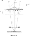
- the bending function of the transfer lens can be done by the plurality of micro-deflectors, and therefore the transfer lens can be removed, as proposed in the first cross reference and shown in Figure 1 . Without the transfer lens, the projection imaging system will be simplified and easy in manufacturing and operation.
- the electron source 101 on the primary optical axis 100_1 generates the primary electron beam 102 with a source crossover (virtual or real) 101s.
- the condenser lens 110 focuses the primary-electron beam 102 incident onto the source-conversion unit 120 with a desired current density.
- the peripheral electrons of the primary electron beam 102 are cut off by the main opening of the main aperture plate 171, which can also be placed above the condenser lens 110.
- Three beamlets (102_1, 102_2 and 102_3) of the primary-electron beam 102 are respectively deflected towards the primary optical axis 100_1 by the three micro-deflectors (122_1, 122_2 and 122_3) of the image-forming mean 122, and pass through three beam-limit openings (121_1, 121_2 and 121_3) of the beamlet-limit means 121. Then, the three virtual images (102_1v, 102_2v and 102_3v) formed by the deflected three beamlets are projected by the objective lens 131 onto the surface 7 of the sample 8 and three probe spots (102_1s, 102_2s and 102_3s) therefore are formed thereon.
- the three beamlets are deflected close to or passing through the front focal point of the objective lens 131, they will perpendicularly land on the sample surface 7 and aberrations of the off-axis probe spots (such as 102_2s) due to the objective lens 131 will decrease to a great degree.
- the deflection angles of the three beamlets become larger, which not only require stronger deflection powers of the three micro-deflectors but also generate larger deflection aberrations.
- the first issue may incur electric breakdown of the three micro-deflectors, and the second issue may enlarge the sizes of the off-axis probe spots to an unacceptable level.
- the beam-limit openings limit the currents of the three probe spots, and the currents are changed by tuning the focusing power of the condenser lens 110 to vary the current density of the primary electron beam 102.
- the incident angles of the three beamlets change with the focusing power, and the deflection powers thereof need adjusting accordingly.
- the time and the effort for changing observing conditions are the less the better.
- a multi-beam apparatus which has no or fewer foregoing issues, and therefore can provide high image resolution and high throughput.
- a multi-beam apparatus which can inspect and/or review defects on wafers/masks with high resolution and high throughput is needed to match the roadmap of the semiconductor manufacturing industry.
- the object of this invention is to provide a new multi-beam apparatus which provide both high resolution and high throughput for observing a sample in flexibly varying observing conditions (such as currents and landing energies of the probe spots, electrostatic field on the sample surface).
- the apparatus can function as a yield management tool to inspect and/or review defects on wafers/masks in semiconductor manufacturing industry.
- one condenser collimates or substantially collimates the primary-electron beam into one source-conversion unit
- the source-conversion unit deflects a plurality of beamlets of the primary-electron beam towards the optical axis of one objective lens
- the objective lens focuses the plurality of deflected beamlets onto one being-observed surface of one sample and therefore a plurality of probe spots is formed thereon, wherein the deflection angles of the plurality of deflected beamlets are adjusted to reduce the sizes of the plurality of probe spots.
- the currents of the plurality of probe spots can be varied by changing either or both of the focusing power and the position of the first principal plane of the condenser lens.
- the source-conversion unit can further reduce the sizes and the size differences of the plurality of probe spots by compensating off-axis aberrations thereof. Furthermore, to weaken the Coulomb effect due to the primary-electron beam as much as possible, the beamlet-forming means of the source conversion unit can be placed close to the single electron source, a pre-beamlet-forming means can be employed close to the single electron source.
- the invention therefore provides a multi-beam apparatus, which comprises an electron source, a condenser lens below the electron source, a source-conversion unit below the condenser lens, an objective lens below the source-conversion unit, a deflection scanning unit below the source-conversion unit, a sample stage below the objective lens, a beam separator below the source-conversion unit, a secondary projection imaging system, and an electron detection device with a plurality of detection elements.
- the electron source, the condenser lens and the objective lens are aligned with a primary optical axis of the apparatus, and the sample stage sustains the sample so that the surface faces to the objective lens.
- the source-conversion unit comprises a beamlet-forming means with a plurality of beam-limit openings and an image-forming means with a plurality of electron optics elements.
- the electron source generates a primary-electron beam along the primary optical axis, and the primary-electron beam is focused by the condenser lens to become a substantially parallel beam and then incident into the source-conversion unit.
- a plurality of beamlets of the primary-electron beam exits from the source-conversion unit, which respectively passes through the plurality of beam-limit openings and is deflected by the plurality of electron optics elements towards the primary optical axis, and deflection angles of the plurality of beamlets are different.
- the plurality of beamlets focused by the objective lens onto the surface and forms a plurality of probe spots thereon, is deflected by the deflection scanning unit to scan the plurality of probe spots respectively over a plurality of scanned regions within an observed area on the surface, and currents of the plurality of probe spots are limited by the plurality of beam-limit openings.
- a plurality of secondary electron beams generated by the plurality of probe spots respectively from the plurality of scanned regions and directed into the secondary projection imaging system by the beam separator, is focused by the secondary projection imaging system to keep the plurality of secondary electron beams to be detected by the plurality of detection elements respectively, and each detection element therefore provides an image signal of one corresponding scanned region.
- the deflection angles can be individually set to reduce aberrations of the plurality of probe spots respectively.
- the plurality of electron optics elements is below and aligned with the plurality of beam-limit openings respectively.
- Each of the plurality of electron optics elements can be a 4-pole lens.
- Currents of the plurality of probe spots are varied by using the condenser lens to change a current density of the primary-electron beam incident into the source-conversion unit.
- the apparatus may further comprise a pre-beamlet-forming means with a plurality of beamlet-forming apertures above the source-conversion unit, wherein the plurality of beamlets passes through the plurality of beamlet-forming apertures respectively and most of electrons outside the plurality of beamlets are cut off.
- the plurality of electron optics elements can compensate one or up to all of field curvature, astigmatism and distortion aberrations of the plurality of probe spots to further reduce sizes and distortions thereof.
- Each of the plurality of electron optics elements can be an 8-pole lens.
- Each of the plurality of electron optics elements may comprise one micro-lens and two 4-pole lenses which are aligned with and placed along an optical axis of the each element, and the two 4-pole lenses have a 45° difference in azimuth. For that each of the plurality of electron optics elements, one of the two 4-pole lenses is on a beamlet exit side and one corresponding beamlet is deflected by the one 4-pole lens.
- the condenser lens in one embodiment, may comprise multiple annular electrodes which are placed at different axial positions along and aligned with the primary optical axis, and voltages thereof can be adjusted to change the current density.
- the condenser lens in another embodiment, may comprise at least two single magnetic lenses which are placed at different axial positions along and aligned with the primary optical axis, and excitations thereof can be adjusted to change the current density of the primary-electron beam incident into the source-conversion unit.
- the condenser lens in still another embodiment, may comprise multiple annular electrodes and at least one single magnetic lens which are placed at different axial positions along and aligned with the primary optical axis, and voltages of the electrodes and excitations of the at least one single magnetic lens can be adjusted to change the current density.
- Landing energies of the plurality of beamlets on the surface are varied by changing a potential thereof.
- the present invention also provides a multi-beam apparatus, which comprises an electron source, a condenser lens below the electron source, a source-conversion unit below the condenser lens, an objective lens below the source-conversion unit, a deflection scanning unit below the source-conversion unit, a sample stage below the objective lens, a beam separator below the source-conversion unit, a secondary projection imaging system, and an electron detection device with a plurality of detection elements.
- the electron source, the condenser lens and the objective lens are aligned with a primary optical axis of the apparatus, and the sample stage sustains the sample so that the surface faces to the objective lens.
- the source-conversion unit comprises a beamlet-forming means with a plurality of beam-limit openings and an image-forming means with a plurality of electron optics elements.
- the electron source generates a primary-electron beam along the primary optical axis, which is focused by the condenser lens, and then is incident into the source-conversion unit with a convergent or divergent angle.
- a plurality of beamlets of the primary-electron beam exits from the source-conversion unit, respectively passes through the plurality of beam-limit openings, and is deflected by the plurality of electron optics elements towards the primary optical axis.
- the plurality of beamlets is focused by the objective lens onto the surface and forms a plurality of probe spots thereon.
- Deflection angles of the plurality of beamlets are individually set to reduce aberrations of the plurality of probe spots respectively, and the deflection scanning unit deflects the plurality of beamlets to scan the plurality of probe spots respectively over a plurality of scanned regions within an observed area on the surface. Currents of the plurality of probe spots are limited by the plurality of beam-limit openings.
- the secondary projection imaging system focuses and keeps the plurality of secondary electron beams to be detected by the plurality of detection elements respectively, and each detection element therefore provides an image signal of one corresponding scanned region.
- the plurality of electron optics elements could compensate one or up to all of field curvature, astigmatism and distortion aberrations of the plurality of probe spots to further reduce sizes and distortions thereof.
- Currents of the plurality of probe spots are varied by using the condenser lens to adjust a current density of the primary-electron beam incident into the source-conversion unit.
- the plurality of electron optics elements may be below the plurality of beam-limit openings.
- the apparatus may further comprise a pre-beamlet-bending means with a plurality of pre-bending micro-deflectors respectively above the plurality of beam-limit openings.
- the plurality of pre-bending micro-deflectors may deflect the plurality of beamlets to be perpendicularly incident into the plurality of beam-limit openings.
- the apparatus may further comprise a pre-beamlet-forming means with a plurality of beamlet-forming apertures above the source-conversion unit, wherein the plurality of beamlets passes through the plurality of beamlet-forming apertures respectively and most of electrons outside the plurality of beamlets are cut off.
- the present invention also provides a multi-beam apparatus, which comprises an electron source, a beamlet-forming plate providing a plurality of beam-limit openings below the electron source, a condenser lens below the beamlet-forming plate, a plurality of electron optics elements below the condenser lens, an objective lens below the plurality of electron optics elements, a deflection scanning unit below the plurality of electron optics elements, a sample stage below the objective lens, a beam separator below the plurality of electron optics elements, a secondary projection imaging system, and an electron detection device with a plurality of detection elements.
- the electron source, the condenser lens and the objective lens are aligned with a primary optical axis of the apparatus, and the sample stage sustains the sample so that the surface faces to the objective lens.
- the electron source generates a primary-electron beam along the primary optical axis, which is trimmed by the beamlet-forming plate into a plurality of beamlets respectively passing through a plurality of through-holes of a first group therein, and the plurality of through-holes functions as a plurality of beam-limit openings of the apparatus.
- the condenser lens focuses the plurality of beamlets to be deflected by the plurality of electron optics elements respectively towards the primary optical axis.
- the plurality of beamlets is focused by the objective lens onto the surface and forms a plurality of probe spots thereon, and deflection angles of the plurality of beamlets are individually set to reduce aberrations of the plurality of probe spots respectively.
- the deflection scanning unit deflects the plurality of beamlets to scan the plurality of probe spots respectively over a plurality of scanned regions within an observed area on the surface, and currents of the plurality of probe spots are limited by the plurality of beam-limit openings.
- a plurality of secondary electron beams is generated by the plurality of probe spots respectively from the plurality of scanned regions and directed into the secondary projection imaging system by the beam separator.
- the secondary projection imaging system focuses and keeps the plurality of secondary electron beams to be detected by the plurality of detection elements respectively, and each detection element therefore provides an image signal of one corresponding scanned region.
- the plurality of beamlets is perpendicularly incident into the plurality of electron optics elements.
- the plurality of electron optics elements compensates one or up to all of field curvature, astigmatism and distortion aberrations of the plurality of probe spots to further reduce sizes and distortions thereof.
- Currents of the plurality of beamlets in one embodiment, can be varied by adjusting an angular intensity of the electron source.
- Currents of the plurality of beamlets in another embodiment, can be varied by changing radial sizes of the plurality of beam-limit openings. The radial sizes are changed by moving the beamlet-forming plate to locate a plurality of through-holes of a second group therein as the plurality of beam-limit openings.
- the present invention also provides a method to form a plurality of probe spots in a SEM, which comprises steps of generating a primary-electron beam by an electron source, collimating or substantially collimating the primary-electron beam by a condenser lens, trimming the collimated primary-electron beam into a plurality of beamlets by a first plate with first through-holes, deflecting the plurality of beamlets towards an optical axis of an objective lens with different deflection angles by a plurality of electron optics elements, and focusing the plurality of deflected beamlets onto a being-observed surface of a sample by the objective lens, wherein the plurality of deflected and focused beamlets forms the plurality of probe spots.
- the method may further comprise a step of individually setting the deflection angles to reduce aberrations of the plurality of probe spots respectively.
- the method may further comprise a step of compensating one or up to all of field curvature, astigmatism and distortion aberrations of the plurality of probe spots by the plurality of electron optics elements.
- the method may further comprise a step of varying a current density of the collimated primary-electron beam by moving a first principal plane of the condenser lens.
- the method may further comprise a step of cutting off most of electrons outside the plurality of beamlets by a second plate with second through-holes before the trimming step.
- the present invention also provides a method to form a plurality of probe spots in a SEM, which comprises generating a primary-electron beam by an electron source, trimming the primary-electron beam into a plurality of beamlets by a plate with a plurality of through-holes, focusing the plurality of beamlets by a condenser lens, deflecting the plurality of beamlets towards an optical axis of an objective lens by a plurality of electron optics elements, focusing the plurality of deflected beamlets onto a being-observed surface of a sample by the objective lens, wherein the plurality of deflected and focused beamlets forms the plurality of probe spots, and setting deflection angles of the plurality of deflected beamlets individually to reduce aberrations of the plurality of probe spots respectively.
- the method may further comprise a step of compensating one or up to all of field curvature, astigmatism and distortion aberrations of the plurality of probe spots by the plurality of electron optics elements.
- the method may further comprise a step of varying currents of the plurality of beamlets by changing an angular intensity of the electron source.
- the method may further comprise a step of changing currents of the plurality of beamlets by using another plurality of through-holes of the plate in the trimming step.
- the present invention also provides a device for providing multiple sources, which comprises a charged-particle source for providing a primary beam along an optical axis of the device, means for substantially collimating the primary beam, and means for imaging a plurality of virtual images of the charged-particle source with a plurality of beamlets of the collimated primary beam, wherein the plurality of virtual images becomes the multiple sources which emit the plurality of beamlets respectively.
- the device may further comprise means for varying currents of the plurality of beamlets.
- the device may further comprise means for suppressing Coulomb effect due to the primary beam.
- the present invention also provides a multi-beam apparatus, which comprises the device for providing the multiple sources, means for projecting the plurality of virtual images on a sample surface such that a plurality of probe spots is formed thereon, means for scanning the plurality of probe spots on the sample surface, and means for receiving a plurality of signal particle beams generated from the sample surface due to plurality of probe spots.
- the multi-beam apparatus may further comprise means for individually deflecting the plurality of beamlets to reduce aberrations of the plurality of probe spots respectively.
- the multi-beam apparatus may further comprise means for individually compensating the aberrations of the plurality of probe spots.
- the projecting means is a single objective lens.
- axial means “in the optical axis direction of an electron optics element (such as a round lens or a multipole lens), or an apparatus”
- radial means “in a direction perpendicular to the optical axis”
- on-axial means “on or aligned with the optical axis”
- off-axis means “not on or not aligned with the optical axis”.
- X, Y and Z axe form Cartesian coordinate
- the optical axis is on the Z-axis and a primary-electron beam travels along the Z-axis.
- primary electrons means “electrons emitted from an electron source and incident onto a being-observed or inspected surface of a sample
- secondary electrons means “electrons generated from the surface by the "primary electrons”
- the primary-electron beam is focused parallel or substantially parallel into one source-conversion unit by one condenser.
- a plurality of beamlets of the primary-electron beam is at first deflected by the source-conversion unit towards the optical axis of one objective lens, then focused by the objective lens onto the sample surface, and finally forms a plurality of probe spots thereon.
- the deflection angles of the plurality of deflected beamlets are set to minimize the off-axis aberrations due to the objective lens.
- the currents of the plural probe spots can be varied by changing either or both of the focusing power and the position of the first principal plane of the condenser lens, and the sizes and their size differences of the plural probe spots can be further reduced by compensating the residual off-axis aberrations by the source-conversion unit.
- the blurs due to strong Coulomb effect of the primary-electron beam can be reduced by placing the beamlet-forming means of the source-conversion unit close to the single electron source or additionally using one pre-beamlet-forming means above the source-conversion unit.
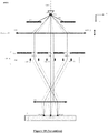
- FIG. 2 One embodiment 200A of the new apparatus is shown in Figure 2 .
- the election source 101, the main opening of the main aperture plate 271, the condenser 210, the source-conversion unit 220 and the objective lens 131 are aligned with the primary optical axis 200_1 of the apparatus.
- the electron source 101 generates a primary-electron beam 102 along the primary optical axis 200_1 and with a source crossover (virtual or real) 101s, the condenser lens 210 focuses the primary-electron beam 102 to become a parallel beam along the primary optical axis 200_1 and perpendicularly incident onto the source-conversion unit 220.
- three beamlets 102_1, 102_2 and 102_3 of the primary-electron beam 102 are respectively deflected by three micro-deflectors 222_1d, 222_2d and 222_3d of the image-forming means 222 towards the primary optical axis 200_1 and pass through three beam-limit openings 221_1, 221_2 and 221_3 of the beamlet-limit means 221.
- the three beam-limit openings limit currents of the three deflected beamlets.
- the objective lens 131 focuses the three deflected beamlets onto the surface 7 of the sample 8, and accordingly generates three images 102_1s, 102_2s and 102_3s of the source crossover 101s thereon.
- Each image forms one probe spot on the surface 7, and the three images are also called as three probe spots 102_1s, 102_2s and 102_3s.
- the deflection angles of the three deflected beamlets are set to minimize the off-axis aberrations of the three images due to the objective lens 131, wherein the three deflected beamlets typically pass through or approach the front focal point of the objective lens 131.
- the main aperture plate 271 cuts the peripheral electrons of the primary-electron beam 102 to reduce the Coulomb Effect thereof as much as possible.
- the beamlet-forming means 221 can be an electric-conduction plate with through-holes, and three through-holes therein function as the three beam-limit openings (221_1 ⁇ 221_3) respectively.
- the three deflected beamlets (102_1 ⁇ 102_3) do not perpendicularly pass through the three beam-limit openings (221_1 ⁇ 221_3), and therefore suffers electron scatterings to a certain degree related to the deflection angles.
- the scattering electrons in each beamlet will enlarge the probe spot and/or become a background noise and therefore deteriorate the image resolution of the corresponding scanned region.
- the currents of the three beamlets can be cut when the three beamlets are parallel to the primary optical axis 200_1.
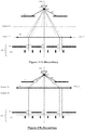
- FIG. 3 Another embodiment 300A of the new apparatus is proposed in Figure 3 .
- the beamlet-limit means 221 is placed above the image-forming means 222 and renamed as beamlet-forming means 321 in the source-conversion unit 320 in Figure 3 .
- the three beam-limit openings 321_1, 321_2 and 321_3 of the beamlet-forming means 321 are respectively aligned with the three micro-deflectors 222_1d, 222_2d and 222_3d of the image-forming means 222, and the three beamlets 102_1, 102_2 and 102_3 are perpendicularly incident into the three beam-limit openings and the three micro-deflectors in succession.
- the condenser lens 210 and the objective lens 131 generate off-axis aberrations (such as field curvature, astigmatism and distortion) which enlarge the sizes and/or influence the positions of the probe spots formed by those off-axis beamlets (not along the primary optical axis of the apparatus).
- off-axis aberrations due to the objective lens 131 have been minimized by individually optimizing the trajectories of the off-axis beamlets (i.e. appropriately setting the deflection angles thereof).
- the off-axis aberrations due to the condenser lens 210 and the residual off-axis aberrations due to the objective lens 131 have to be compensated.
- FIG. 4 Another embodiment 400A of the new apparatus is proposed in Figure 4 , wherein the image-forming means 422 has three micro-deflector-and-compensator elements 422_1dc, 422_2dc and 422_3dc.
- Each micro-deflector-and-compensator element is aligned with one of three beam-limit openings 321_1, 321_2 and 321_3 of the beamlet-forming means 321, functions as one micro-deflector to deflect one beamlet and one micro-compensator to compensate the field curvature, astigmatism and distortion of the corresponding probe spot.
- Each of three micro-deflectors (222_1d ⁇ 222_3d) in Figure 2 and Figure 3 can simply be formed by a dipole lens whose two electrodes is oriented to generate a dipole field in the required deflection direction of the corresponding beamlet, or a quadrupole or 4-pole lens whose four electrodes can generate a dipole field in any desired direction.
- all the micro-deflectors can be configured to be same in structure and orientation. This is advantageous from the manufacturing point of view.
- each of three micro-deflector-and-compensator elements (422_1dc ⁇ 422_3d) can simply be formed by a 4-pole lens whose four electrodes can generate a dipole field in any desired direction, a round-lens field and a quadrupole field in the required compensation direction of the corresponding probe spot, or a octupole or 8-pole lens whose eight electrodes can generate a round-lens field, a dipole field and a quadrupole field both in any desired direction.
- the inner surfaces of the four or the eight electrodes form a circular shape in a radial cross-section, as shown in Figure 5 .
- all the micro-deflector-and-compensator elements can be configured to be same in structure and orientation. This is advantageous from the manufacturing point of view.
- each micro-deflector-and-compensator element can be formed by two or more micro-multipole-lenses, or one or more micro-multipole-lenses and one or more micro-lens.
- the corresponding beamlet is better passing through the round-lens field and the quadrupole field along the optical axis thereof, i.e. the off-axis aberration compensation is better done before the beamlet deflection.
- FIG. 6A shows such an embodiment of the image-forming means 422 in Figure 4 , wherein each of three micro-deflector-and-compensator elements (422_1dc ⁇ 422_3dc) is formed by one micro-lens in the first layer 422-1, one micro-multipole-lens in the second layer 422-2 and one micro-multipole-lens in the third layer 422-3, and the micro-lens and the two micro-multipole-lenses are aligned with its optical axis.
- micro-lens 422-1_2 and two micro-multipole-lenses 422-2_2 and 422-3_2 form the micro-deflector-and-compensator element 422_2dc and are aligned with the optical axis 422_2dc_1 thereof.
- each micro-deflector-and-compensator element in Figure 6A the two micro-multipole-lenses can respectively be a dipole lens and a 4-pole lens, or a dipole lens and an 8-pole lens, or a 4-pole lens, etc.
- Figures 6B, 6C and 6D show one example, wherein each micro-lens is formed by one annular electrode with a round inner surface, each micro-multipole-lens is a 4-pole lens, and each 4-pole lens in the second layer 422-2 and the corresponding 4-pole lens in the third layer 422-3 have a 45° difference in azimuth or orientation.
- the micro-lens For each micro-deflector-and-compensator element, the micro-lens generates the round-lens field, the two 4-pole lenses generate the quadrupole field, and the dipole field is better generated by the 4-pole lens in the third layer 422-3.
- the image-forming means 422 can comprises one electric-conduction coverplate which has a plurality of through-holes and is placed above the electrodes of all the micro-lens-and-compensator elements. Each through-hole is for the corresponding beamlet passing through.
- FIG. 7A shows one way to implement the foregoing measures in the embodiment in Figure 6A .
- the first-upper and the first-lower electric-conduction plates 422-1-CL1 and 422-1-CL2 are respectively placed above and below the micro-lens 422-1_1, 422-1_2 and 422-1_3 in the first layer 422-1.
- the second-upper and the second-lower electric-conduction plates 422-2-CL1 and 422-2-CL2 are respectively placed above and below the micro-multipole-lenses 422-2_1, 422-2_2 and 422-2_3.
- the third-upper and the third-lower electric-conduction plates 422-3-CL1 and 422-3-CL2 and the third-upper and the third-lower insulator plates 422-3-IL1 and 422-3-IL2 function the same ways as their counterparts in the second layer 422-2.
- each through-hole in the first-upper electric-conduction plate is preferred in an upside-down funnel shape (i.e. the small end is on the beamlet incident side thereof).
- the beamlet-forming means 321 can be an electric-conduction plate with through-holes, and three through-holes therein functions as the three beam-limit openings (321_1 ⁇ 321_3) respectively. Therefore the beamlet-forming means 321 can be combined with the embodiment of the image-forming means 422 in 7A for simplifications in structure and manufacturing.
- Figure 7B the beamlet-forming means 321 and the first-upper electric-conduction plate 422-1-CL1 are combined, the first-lower electric-conduction plate 422-1-CL2 and the second-upper electric-conduction plate 422-2-CL1 are combined, and the second-lower electric-conduction plate 422-2-CL2 and the third-upper electric-conduction plate 422-3-CL1 are combined.
- the currents of the probe spots 102_1s ⁇ 102_3 can be varied within a small range by adjusting the focusing power of the condenser lens 210 to make the primary-electron beam 102 slightly divergent or convergent.
- Figure 8 shows one divergent mode in the embodiment 300 in Figure 3 . In one divergent mode, the current density of the primary-electron beam 102 is smaller than that in the parallel mode in Figure 3 , and therefore the currents of the three beamlets below the beamlet-forming means 321 are reduced.
- one pre-beamlet-bending means can be placed above the beamlet-forming means 321 of the source-conversion unit 320 in Figure 3 or 420 in Figure 4 , which comprises three pre-bending micro-deflectors to respectively deflect the three beamlets perpendicularly passing through the three beam-limit openings.
- Figure 9 shows how to implement this way in the embodiment 300A in Figure 3 , and in one divergent mode how to operate three pre-bending micro-deflectors 523_1d, 523_2d and 523_3d of the pre-beamlet-bending means 523 of the new source-conversion unit 520 in the corresponding embodiment 500A.
- the currents of the probe spots 102_1s ⁇ 102_3 can be varied within a large range by moving the first principal plane of the condenser 210 and accordingly adjusting the focusing power of the condenser lens 210 to make the primary-electron beam 102 become a parallel beam, i.e. the first principal plane of the condenser lens 210 is movable along the primary optical axis of the new apparatus.
- the first principal plane is closer to the electron source 101, the primary-electron beam 102 is focused earlier and with a higher current density, and accordingly the currents of the three beamlets below the beamlet-forming means 321 are increased.
- Figure 10 shows one embodiment 600A which uses a movable condenser lens 610 to replace the condense lens 210 in the embodiment 300A in Figure 3 , wherein the first principal plane 610_2 is at position P1 and can be moved along the primary optical axis 600_1 of the apparatus.
- the first principal plane 610_2 is moved from the position P1 to the position P2 further away from the electron source 101, and accordingly the currents of the beamlets 102_1, 102_2 and 102_3 decrease.
- Figure 11B the first principal plane 610_2 is moved from the position P1 to the position P3 closer to the electron source 101, and accordingly the currents of the beamlets 102_1, 102_2 and 102_3 increase. Due to primary-electron beam 102 is kept as a parallel beam when varying the currents of the beamlets, the deflection angles thereof do not need to be re-tuned. This will avoid the time for adjusting the micro-deflectors.
- the primary-electron beam 102 in Figure 11A can be weakly focused so as to keep a divergence, and the primary-electron beam 102 in Figure 11B can be strongly focused to become a convergent beam.
- the size of each probe spot is determined by the Gaussian image size of the source crossover 101s, the geometrical aberrations, the diffraction effect and the Coulomb Effect, and the size can be minimized by balancing these blurs. Adjusting the position of the first principal plane 610_2 of the movable condenser lens 610 will break the balance to a certain degree, and therefore the size of each probe spot may increase when the current thereof is changed. When changing the position of the first principal plane 610_2, slightly remaining an appropriate divergence or convergence of the primary-electron beam 102 can weaken the size increasing of the probe spots.
- the displacement of the first principal plane 610_2 can be done by mechanically moving the position of the movable condenser lens 610 or electrically moving the position and/or changing the shape of the round-lens field thereof.
- the movable condenser lens 610 can be electrostatic, or magnetic, or electromagnetic compound.
- Figure 12 shows one electrostatic embodiment 610e of the movable condenser lens 610, and shapes of the primary-electron beam 102 when the first principal plane 610e_2 is at the positions PI, P2 and P3 respectively.
- the movable condenser lens 610e is an electrostatic lens with four annular electrodes 610e-e1, 610e-e2, 610e-e3 and 610e-e4 aligned with its optical axis 610e_1.
- the optical axis 610e_1 is placed coincident with the primary optical axis 600_1.
- the focusing power and the position of the first principal plane 610e_2 of the embodiment 610e vary with the excitation mode of the annular electrodes 610e-e1-610e-e4.
- the first principal plane 610e_2 will be at the position P2 close to the electrode 610e-e3 and the primary-electron beam 102 can be collimated over there.
- the electrodes 610e-e1, 610e-e3 and 610e-e4 are at same potentials, by appropriately setting the potential of the electrode 610e-e2, the first principal plane 610e_2 will be at the position P3 close to the electrode 610e-e2 and the primary-electron beam 102 can be collimated over there.
- the first principal plane 610e_2 will be at a position (such as PI) between the electrodes 610e-e2 and 610e-e3 and the primary-electron beam 102 can be collimated over there.
- the current of the primary-electron beam 102 does not change with the position of the first principal plane 610e_2, but its width does and therefore its current density does too.
- the width of the primary-electron beam 102 become smaller and the current density therefore increases. Accordingly, as the first principal plane 610m_2 moves from P3 to P1 and then to P2, the width of the primary-electron beam 102 broadens from 102W_P3 to 102W_P1 and then to 102W_P2. If the electrostatic embodiment 610e comprises more electrodes placed within a longer area along the optical axis 610e_1, the current density can be varied more smoothly within a larger range.
- Figure 13A shows one magnetic embodiment 610m of the movable condenser lens 610 in Figure 10 , and shapes of the primary-electron beam 102 when the first principal plane 610m_2 is at the positions P1, P2 and P3 respectively.
- the movable condenser lens 610m is a compound magnetic lens, which comprises two single magnetic lenses 610m-m1 and 610m-m2 aligned with its optical axis 610m_1.
- the optical axis 610m_1 is placed coincident with the primary optical axis 600_1.
- the focusing power and the position of the first principal plane 610m_2 of the embodiment 610m vary with the excitation mode of the single magnetic lenses 610m-m1 and 610m-m2.
- the first principal plane 610m_2 When the excitation of the single magnetic lens 610m-m2 is set zero, by appropriately setting the excitation of the single magnetic lens 610m-m1, the first principal plane 610m_2 will be at the position P3 within the magnetic-circuit gap thereof and the primary-electron beam 102 can be collimated over there.
- the excitation of the single magnetic lens 610m-m1 is set zero, by appropriately setting the excitation of the single magnetic lens 610m-m2, the first principal plane 610m_2 will be at the position P2 within the magnetic-circuit gap thereof and the primary-electron beam 102 can be collimated over there.
- the first principal plane 610m_2 When the excitations of the single magnetic lenses 610m-m1 and 610m-m2 are not zero, by appropriately setting the excitation ratios thereof, the first principal plane 610m_2 will be at a position (such as PI) between the magnetic-circuit gaps thereof and the primary-electron beam 102 can be collimated over there. Accordingly, as the first principal plane 610m_2 moves from P3 to P1 and then to P2, the width of the primary-electron beam 102 broadens from 102W_P3 to 102W_P1 and then to 102W_P2.
- the magnetic embodiment 610m comprises more single magnetic lenses placed within a longer area along the optical axis 610m_1, the current density of the primary-electron beam 102 can be varied more smoothly within a larger range.
- the neighboring magnetic lenses can share the magnetic circuit therebetween, as shown in Figure 13B .
- the movable condenser lens 610 can also be an electromagnetic-compound lens which comprises multiple annular electrodes and at least one single magnetic lens, and its first principal plane can be moved by adjusting the excitation mode of the annual electrodes and the single magnetic lens.
- the interactions of the primary electrons may be very strong if the energies thereof are not high enough.
- the primary-electron beam 102 passing through the main opening of the main aperture plate 271 only one part is used as the three beamlets (102_1 ⁇ 102_3), and the other part is not useful.
- the current of the other part is higher than the total current of the three beamlets, and therefore generates a stronger Coulomb effect which disturbs the motions of the primary electrons of the three beamlets and consequently increases the sizes of the three probe spots. Hence it is better to cut off all or partial portion of the other part as early as possible. There are several ways to do so.
- Figure 14 shows such an embodiment 700A of the new apparatus.
- the three beamlets 102_1, 102_2 and 102_3 respectively pass through the three beam-limit openings 721_1, 721_2 and 721_3 of the beamlet-forming means 721, and the left part of the primary-electron beam 102 is cut off.
- the condenser lens 210 collimates the three beamlets into the image-forming mean 222, and the three micro-deflectors 222_1d, 222_2d and 222_3d deflect the three beamlets in the way same as Figure 3 .
- each of the off-axis beam-limit openings (such as 721_2) can not be aligned with the corresponding micro-deflector (such as 222_2d) as shown in Figure 3 , and needs to be placed with respect to the influence of the condenser lens 210.
- the currents of the three beamlets can be changed by varying either the emission (angular intensity) of the electron source 101 or the sizes of the beam-limit openings 721_1, 721_2 and 721_3.
- the beamlet-forming means 721 can be an electric-conduction plate with multiple through-hole groups, each through-hole group comprises three through-holes, and the radial sizes of three through-holes in one through-hole group are different from those of three through-holes in another through-hole group.
- Three through-holes in one through-hole group function as the three beam-limit openings (721_1-721_3), and therefore the sizes of the three beam-limit openings can be changed by using different through-hole groups.
- Figure 15A shows such one embodiment 800A of the new apparatus, wherein one pre-beamlet-forming means 872 with three beamlet-forming apertures 872_1, 872_2 and 872_3 is placed above the condenser Lens 210, below and close to the main aperture plate 271.
- the three beamlet-forming apertures cut the wide primary-electron beam 102 into three beamlets 102_1, 102_2 and 102_3, and then the beam-limit openings 321_1, 321_2 and 321_3 cut off the peripheral electrons of the beamlets 102_1, 102_2 and 102_3 and therefore limit the currents thereof.
- the currents of the beamlets 102_1, 102_2 and 102_3 can be changed by varying either the emission of the single electron source or the sizes of the beam-limit openings or using a movable condenser lens as shown in Figure 10 .
- Figure 15B shows such another embodiment 900A of the new apparatus, wherein one pre-beamlet-forming means 972 with three beamlet-forming apertures 972_1, 972_2 and 972_3 is placed below the condenser Lens 210.
- the pre-beamlet-forming means 972 in Figure 15B is not better than the pre-beamlet-forming means 872 in Figure 15A , but it is easier implemented for many obvious reasons and especially when a magnetic movable condenser lens is used to change the currents of the beamlets.
- Figure 16 shows such an embodiment 1000A of the new apparatus, which uses one pre-beamlet-forming means 872 shown in Figure 15A to reduce the Coulomb effect due to the primary-electron beam 102, one movable condenser lens 610 shown in Figure 10 to vary the currents of the probe spots 102_1s ⁇ 102_3s, one image-forming means 422 in Figure 4 to compensate the off-axis aberrations of the probe spots.
- the Coulomb effect due to the primary-electron beam 102 is reduced by employing the pre-beamlet-forming means 972 shown in Figure 15B .
- the landing energies of the plurality of beamlets can be varied by changing either or both of the potential of the emitter in the electron source 101 and the potential of the sample surface 7.
- varying the potential of the sample surface 7 is advantageous because the corresponding adjustment on the source-conversion unit is minor.
- this invention proposes a new multi-beam apparatus which provides both high resolution and high throughput for observing a sample in flexibly varying observing conditions, and therefore can function as a yield management tool to inspect and/or review defects/particles on wafers/masks in semiconductor manufacturing industry.
- one condenser collimates or substantially collimates the primary-electron beam into one source-conversion unit
- the source-conversion unit deflects a plurality of beamlets of the primary-electron beam towards the optical axis of one objective lens
- the objective lens focuses the plurality of deflected beamlets onto the sample surface and therefore a plurality of probe spots is formed thereon, wherein the deflection angles of the plurality of deflected beamlets are adjusted to reduce the sizes of the plurality of probe spots.
- the currents of the plurality of probe spots can be varied within a large range by changing both of the focusing power and the position of the first principal plane of the condenser lens.
- the off-axis aberrations thereof can be compensated by the source-conversion unit and the Coulomb effect due to the primary-electron beam can be weakened by placing the beamlet-forming means of the source conversion unit close to the single electron source or using one pre-beamlet-forming means.
Abstract
Description
- This application claims the benefit of priority of
U.S. provisional application No. 62/195,353 entitled to Ren et al. filed July 22nd, 2015 - This application is related to
U.S. application No. 15/065,342 entitled to Weiming Ren et al. filed on March 9, 2016 and entitled "Apparatus of Plural Charged-Particle Beams", the entire disclosures of which are incorporated herein by reference. - This application is related to U. S. application No.
15/078,369 entitled to Weiming Ren et al. filed on March 23, 2016 - This application is related to U. S. application No.
15/150,858 entitled to Xuedong Liu et al. filed on May 10, 2016 - This application is related to U. S. application No.
15/213/781 entitled to Shuai Li et al. filed on July 19, 2016 - The present invention relates to a charged-particle apparatus with a plurality of charged-particle beams. More particularly, it relates to an apparatus which employs plural charged-particle beams to simultaneously acquire images of plural scanned regions of an observed area on a sample surface. Hence, the apparatus can be used to inspect and/or review defects on wafers/masks with high resolution and high throughput in semiconductor manufacturing industry.
- For manufacturing semiconductor IC chips, pattern defects and/or uninvited particles (residuals) inevitably appear on a wafer and/or a mask during fabrication processes, which reduce the yield to a great degree. To meet the more and more advanced requirements on performance of IC chips, the patterns with smaller and smaller critical feature dimensions have been adopted. Accordingly, the conventional yield management tools with optical beam gradually become incompetent due to diffraction effect, and yield management tools with electron beam are more and more employed. Compared to a photon beam, an electron beam has a shorter wavelength and thereby possibly offering superior spatial resolution. Currently, the yield management tools with electron beam employ the principle of scanning electron microscope (SEM) with a single electron beam, which therefore can provide higher resolution but can not provide throughputs competent for mass production. Although a higher and higher current of the single electron beam can be used to increase the throughputs, the superior spatial resolutions will be fundamentally deteriorated by the Coulomb Effect which increases with the beam current.
- For mitigating the limitation on throughput, instead of using a single electron beam with a large current, a promising solution is to use a plurality of electron beams each with a small current. The plurality of electron beams forms a plurality of probe spots on one being-inspected or observed surface of a sample. The plurality of probe spots can respectively and simultaneously scan a plurality of small scanned regions within a large observed area on the sample surface. The electrons of each probe spot generate secondary electrons from the sample surface where they land on. The secondary electrons comprise slow secondary electrons (energies ≤50eV) and backscattered electrons (energies close to landing energies of the electrons). The secondary electrons from the plurality of small scanned regions can be respectively and simultaneously collected by a plurality of electron detectors. Consequently, the image of the large observed area including all of the small scanned regions can be obtained much faster than that scanned with a single beam.
- The plurality of electron beams can be either from a plurality of electron sources respectively, or from a single electron source. For the former, the plurality of electron beams is usually focused onto and scans the plurality of small scanned regions within a plurality of columns respectively, and the secondary electrons from each scanned region are detected by one electron detector inside the corresponding column. The apparatus therefore is generally called as a multi-column apparatus. The plural columns can be either independent or share a multi-axis magnetic or electromagnetic-compound objective lens (such as
US 8,294,095 ). On the sample surface, the beam interval between two adjacent beams is usually as large as 30∼50mm. - For the latter, a source-conversion unit virtually changes the single electron source into a plurality of sub-sources. The source-conversion unit comprises one beamlet-forming (or beamlet-limit) means with a plurality of beam-limit openings and one image-forming means with a plurality of electron optics elements. The plurality of beam-limit openings divides the primary-electron beam generated by the single electron source into a plurality of sub-beams or beamlets respectively, and the plurality of electron optics elements influence the plurality of beamlets to form a plurality of parallel (virtual or real) images of the single electron source. Each image can be taken as one sub-source which emits one corresponding beamlet. To make more beamlets available, the beamlet intervals are at micro meter level. Naturally, one primary projection imaging system and one deflection scanning unit within one single column are used to project the plurality of parallel images onto and scan the plurality of small scanned regions respectively. The plurality of secondary electron beams therefrom is directed by one beam separator into one secondary projection imaging system, and then focused by the secondary projection imaging system to be respectively detected by a plurality of detection elements of one electron detection device inside the single column. The plurality of detection elements can be a plurality of electron detectors placed side by side or a plurality of pixels of one electron detector. The apparatus therefore is generally called as a multi-beam apparatus.
- The beamlet-forming (or beamlet-limit) means is usually an electric-conduction plate with through-holes, and a plurality of through-holes therein function the plurality of beam-limit openings respectively. Two methods have been used to form the plurality of parallel images by the image-forming means. For the first one, each electron optics element has an electrostatic micro-lens which focuses one beamlet and therefore forms one real image, such as
US7,244,949 . For the second one, each electron optics element has a electrostatic micro-deflector which deflects one beamlet and therefore forms one virtual image, such asUS6,943,349 and first cross reference. The concept of using an electrostatic deflector to form a virtual image of an electron source was used in the famous two-slit electron interference experiments as early as in 1950s (Figure 1 of the paper "The Merli-Missiroli-Pozzi Two-Slit Electron-Interference Experiment" published in Physics in Perspective, 14 (2012) 178-195 by Rodolfo Rosa). Coulomb Effect in the second method is weaker than in the first method due to one real image has a higher current density, and hence the second method is more advantageous for achieving both high throughput and high resolution. - To reduce aberrations of the plurality of probe spots, the primary projection imaging system basically comprises one transfer lens and one objective lens, and the transfer lens bends the plurality of beamlets to pass through the objective lens as close to the optical axis thereof as possible. For a source-conversion unit with the second method, the bending function of the transfer lens can be done by the plurality of micro-deflectors, and therefore the transfer lens can be removed, as proposed in the first cross reference and shown in
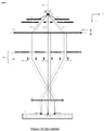
Figure 1 . Without the transfer lens, the projection imaging system will be simplified and easy in manufacturing and operation. - In
Figure 1 , theelectron source 101 on the primary optical axis 100_1 generates theprimary electron beam 102 with a source crossover (virtual or real) 101s. Thecondenser lens 110 focuses the primary-electron beam 102 incident onto the source-conversion unit 120 with a desired current density. The peripheral electrons of theprimary electron beam 102 are cut off by the main opening of themain aperture plate 171, which can also be placed above thecondenser lens 110. Three beamlets (102_1, 102_2 and 102_3) of the primary-electron beam 102 are respectively deflected towards the primary optical axis 100_1 by the three micro-deflectors (122_1, 122_2 and 122_3) of the image-formingmean 122, and pass through three beam-limit openings (121_1, 121_2 and 121_3) of the beamlet-limit means 121. Then, the three virtual images (102_1v, 102_2v and 102_3v) formed by the deflected three beamlets are projected by theobjective lens 131 onto thesurface 7 of the sample 8 and three probe spots (102_1s, 102_2s and 102_3s) therefore are formed thereon. - If the three beamlets are deflected close to or passing through the front focal point of the
objective lens 131, they will perpendicularly land on thesample surface 7 and aberrations of the off-axis probe spots (such as 102_2s) due to theobjective lens 131 will decrease to a great degree. However, in this case, the deflection angles of the three beamlets become larger, which not only require stronger deflection powers of the three micro-deflectors but also generate larger deflection aberrations. The first issue may incur electric breakdown of the three micro-deflectors, and the second issue may enlarge the sizes of the off-axis probe spots to an unacceptable level. - The beam-limit openings limit the currents of the three probe spots, and the currents are changed by tuning the focusing power of the
condenser lens 110 to vary the current density of theprimary electron beam 102. For the three micro-deflectors, the incident angles of the three beamlets change with the focusing power, and the deflection powers thereof need adjusting accordingly. The time and the effort for changing observing conditions are the less the better. - Accordingly, it is necessary to provide a multi-beam apparatus which has no or fewer foregoing issues, and therefore can provide high image resolution and high throughput. Especially, a multi-beam apparatus which can inspect and/or review defects on wafers/masks with high resolution and high throughput is needed to match the roadmap of the semiconductor manufacturing industry.
- The object of this invention is to provide a new multi-beam apparatus which provide both high resolution and high throughput for observing a sample in flexibly varying observing conditions (such as currents and landing energies of the probe spots, electrostatic field on the sample surface). The apparatus can function as a yield management tool to inspect and/or review defects on wafers/masks in semiconductor manufacturing industry.
- In the apparatus, one condenser collimates or substantially collimates the primary-electron beam into one source-conversion unit, the source-conversion unit deflects a plurality of beamlets of the primary-electron beam towards the optical axis of one objective lens, and the objective lens focuses the plurality of deflected beamlets onto one being-observed surface of one sample and therefore a plurality of probe spots is formed thereon, wherein the deflection angles of the plurality of deflected beamlets are adjusted to reduce the sizes of the plurality of probe spots. The currents of the plurality of probe spots can be varied by changing either or both of the focusing power and the position of the first principal plane of the condenser lens. The source-conversion unit can further reduce the sizes and the size differences of the plurality of probe spots by compensating off-axis aberrations thereof. Furthermore, to weaken the Coulomb effect due to the primary-electron beam as much as possible, the beamlet-forming means of the source conversion unit can be placed close to the single electron source, a pre-beamlet-forming means can be employed close to the single electron source.
- Accordingly, the invention therefore provides a multi-beam apparatus, which comprises an electron source, a condenser lens below the electron source, a source-conversion unit below the condenser lens, an objective lens below the source-conversion unit, a deflection scanning unit below the source-conversion unit, a sample stage below the objective lens, a beam separator below the source-conversion unit, a secondary projection imaging system, and an electron detection device with a plurality of detection elements. The electron source, the condenser lens and the objective lens are aligned with a primary optical axis of the apparatus, and the sample stage sustains the sample so that the surface faces to the objective lens. The source-conversion unit comprises a beamlet-forming means with a plurality of beam-limit openings and an image-forming means with a plurality of electron optics elements. The electron source generates a primary-electron beam along the primary optical axis, and the primary-electron beam is focused by the condenser lens to become a substantially parallel beam and then incident into the source-conversion unit. A plurality of beamlets of the primary-electron beam exits from the source-conversion unit, which respectively passes through the plurality of beam-limit openings and is deflected by the plurality of electron optics elements towards the primary optical axis, and deflection angles of the plurality of beamlets are different. The plurality of beamlets, focused by the objective lens onto the surface and forms a plurality of probe spots thereon, is deflected by the deflection scanning unit to scan the plurality of probe spots respectively over a plurality of scanned regions within an observed area on the surface, and currents of the plurality of probe spots are limited by the plurality of beam-limit openings. A plurality of secondary electron beams, generated by the plurality of probe spots respectively from the plurality of scanned regions and directed into the secondary projection imaging system by the beam separator, is focused by the secondary projection imaging system to keep the plurality of secondary electron beams to be detected by the plurality of detection elements respectively, and each detection element therefore provides an image signal of one corresponding scanned region.
- In one embodiment, the deflection angles can be individually set to reduce aberrations of the plurality of probe spots respectively. The plurality of electron optics elements is below and aligned with the plurality of beam-limit openings respectively. Each of the plurality of electron optics elements can be a 4-pole lens. Currents of the plurality of probe spots are varied by using the condenser lens to change a current density of the primary-electron beam incident into the source-conversion unit. The apparatus may further comprise a pre-beamlet-forming means with a plurality of beamlet-forming apertures above the source-conversion unit, wherein the plurality of beamlets passes through the plurality of beamlet-forming apertures respectively and most of electrons outside the plurality of beamlets are cut off.
- The plurality of electron optics elements, in this embodiment, can compensate one or up to all of field curvature, astigmatism and distortion aberrations of the plurality of probe spots to further reduce sizes and distortions thereof. Each of the plurality of electron optics elements can be an 8-pole lens. Each of the plurality of electron optics elements may comprise one micro-lens and two 4-pole lenses which are aligned with and placed along an optical axis of the each element, and the two 4-pole lenses have a 45° difference in azimuth. For that each of the plurality of electron optics elements, one of the two 4-pole lenses is on a beamlet exit side and one corresponding beamlet is deflected by the one 4-pole lens.
- The condenser lens, in one embodiment, may comprise multiple annular electrodes which are placed at different axial positions along and aligned with the primary optical axis, and voltages thereof can be adjusted to change the current density. The condenser lens, in another embodiment, may comprise at least two single magnetic lenses which are placed at different axial positions along and aligned with the primary optical axis, and excitations thereof can be adjusted to change the current density of the primary-electron beam incident into the source-conversion unit. The condenser lens, in still another embodiment, may comprise multiple annular electrodes and at least one single magnetic lens which are placed at different axial positions along and aligned with the primary optical axis, and voltages of the electrodes and excitations of the at least one single magnetic lens can be adjusted to change the current density.
- Landing energies of the plurality of beamlets on the surface are varied by changing a potential thereof.
- The present invention also provides a multi-beam apparatus, which comprises an electron source, a condenser lens below the electron source, a source-conversion unit below the condenser lens, an objective lens below the source-conversion unit, a deflection scanning unit below the source-conversion unit, a sample stage below the objective lens, a beam separator below the source-conversion unit, a secondary projection imaging system, and an electron detection device with a plurality of detection elements. The electron source, the condenser lens and the objective lens are aligned with a primary optical axis of the apparatus, and the sample stage sustains the sample so that the surface faces to the objective lens. The source-conversion unit comprises a beamlet-forming means with a plurality of beam-limit openings and an image-forming means with a plurality of electron optics elements. The electron source generates a primary-electron beam along the primary optical axis, which is focused by the condenser lens, and then is incident into the source-conversion unit with a convergent or divergent angle. A plurality of beamlets of the primary-electron beam exits from the source-conversion unit, respectively passes through the plurality of beam-limit openings, and is deflected by the plurality of electron optics elements towards the primary optical axis. The plurality of beamlets is focused by the objective lens onto the surface and forms a plurality of probe spots thereon. Deflection angles of the plurality of beamlets are individually set to reduce aberrations of the plurality of probe spots respectively, and the deflection scanning unit deflects the plurality of beamlets to scan the plurality of probe spots respectively over a plurality of scanned regions within an observed area on the surface. Currents of the plurality of probe spots are limited by the plurality of beam-limit openings. A plurality of secondary electron beams, generated by the plurality of probe spots respectively from the plurality of scanned regions and directed into the secondary projection imaging system by the beam separator. The secondary projection imaging system focuses and keeps the plurality of secondary electron beams to be detected by the plurality of detection elements respectively, and each detection element therefore provides an image signal of one corresponding scanned region.
- The plurality of electron optics elements could compensate one or up to all of field curvature, astigmatism and distortion aberrations of the plurality of probe spots to further reduce sizes and distortions thereof. Currents of the plurality of probe spots are varied by using the condenser lens to adjust a current density of the primary-electron beam incident into the source-conversion unit. The plurality of electron optics elements may be below the plurality of beam-limit openings. The apparatus may further comprise a pre-beamlet-bending means with a plurality of pre-bending micro-deflectors respectively above the plurality of beam-limit openings. The plurality of pre-bending micro-deflectors may deflect the plurality of beamlets to be perpendicularly incident into the plurality of beam-limit openings. The apparatus may further comprise a pre-beamlet-forming means with a plurality of beamlet-forming apertures above the source-conversion unit, wherein the plurality of beamlets passes through the plurality of beamlet-forming apertures respectively and most of electrons outside the plurality of beamlets are cut off.
- The present invention also provides a multi-beam apparatus, which comprises an electron source, a beamlet-forming plate providing a plurality of beam-limit openings below the electron source, a condenser lens below the beamlet-forming plate, a plurality of electron optics elements below the condenser lens, an objective lens below the plurality of electron optics elements, a deflection scanning unit below the plurality of electron optics elements, a sample stage below the objective lens, a beam separator below the plurality of electron optics elements, a secondary projection imaging system, and an electron detection device with a plurality of detection elements. The electron source, the condenser lens and the objective lens are aligned with a primary optical axis of the apparatus, and the sample stage sustains the sample so that the surface faces to the objective lens. The electron source generates a primary-electron beam along the primary optical axis, which is trimmed by the beamlet-forming plate into a plurality of beamlets respectively passing through a plurality of through-holes of a first group therein, and the plurality of through-holes functions as a plurality of beam-limit openings of the apparatus. The condenser lens focuses the plurality of beamlets to be deflected by the plurality of electron optics elements respectively towards the primary optical axis. The plurality of beamlets is focused by the objective lens onto the surface and forms a plurality of probe spots thereon, and deflection angles of the plurality of beamlets are individually set to reduce aberrations of the plurality of probe spots respectively. The deflection scanning unit deflects the plurality of beamlets to scan the plurality of probe spots respectively over a plurality of scanned regions within an observed area on the surface, and currents of the plurality of probe spots are limited by the plurality of beam-limit openings. A plurality of secondary electron beams is generated by the plurality of probe spots respectively from the plurality of scanned regions and directed into the secondary projection imaging system by the beam separator. The secondary projection imaging system focuses and keeps the plurality of secondary electron beams to be detected by the plurality of detection elements respectively, and each detection element therefore provides an image signal of one corresponding scanned region.
- The plurality of beamlets is perpendicularly incident into the plurality of electron optics elements. The plurality of electron optics elements compensates one or up to all of field curvature, astigmatism and distortion aberrations of the plurality of probe spots to further reduce sizes and distortions thereof. Currents of the plurality of beamlets, in one embodiment, can be varied by adjusting an angular intensity of the electron source. Currents of the plurality of beamlets, in another embodiment, can be varied by changing radial sizes of the plurality of beam-limit openings. The radial sizes are changed by moving the beamlet-forming plate to locate a plurality of through-holes of a second group therein as the plurality of beam-limit openings.
- The present invention also provides a method to form a plurality of probe spots in a SEM, which comprises steps of generating a primary-electron beam by an electron source, collimating or substantially collimating the primary-electron beam by a condenser lens, trimming the collimated primary-electron beam into a plurality of beamlets by a first plate with first through-holes, deflecting the plurality of beamlets towards an optical axis of an objective lens with different deflection angles by a plurality of electron optics elements, and focusing the plurality of deflected beamlets onto a being-observed surface of a sample by the objective lens, wherein the plurality of deflected and focused beamlets forms the plurality of probe spots.
- The method may further comprise a step of individually setting the deflection angles to reduce aberrations of the plurality of probe spots respectively. The method may further comprise a step of compensating one or up to all of field curvature, astigmatism and distortion aberrations of the plurality of probe spots by the plurality of electron optics elements. The method may further comprise a step of varying a current density of the collimated primary-electron beam by moving a first principal plane of the condenser lens. The method may further comprise a step of cutting off most of electrons outside the plurality of beamlets by a second plate with second through-holes before the trimming step.
- The present invention also provides a method to form a plurality of probe spots in a SEM, which comprises generating a primary-electron beam by an electron source, trimming the primary-electron beam into a plurality of beamlets by a plate with a plurality of through-holes, focusing the plurality of beamlets by a condenser lens, deflecting the plurality of beamlets towards an optical axis of an objective lens by a plurality of electron optics elements, focusing the plurality of deflected beamlets onto a being-observed surface of a sample by the objective lens, wherein the plurality of deflected and focused beamlets forms the plurality of probe spots, and setting deflection angles of the plurality of deflected beamlets individually to reduce aberrations of the plurality of probe spots respectively.
- The method may further comprise a step of compensating one or up to all of field curvature, astigmatism and distortion aberrations of the plurality of probe spots by the plurality of electron optics elements. The method may further comprise a step of varying currents of the plurality of beamlets by changing an angular intensity of the electron source. The method may further comprise a step of changing currents of the plurality of beamlets by using another plurality of through-holes of the plate in the trimming step.
- The present invention also provides a device for providing multiple sources, which comprises a charged-particle source for providing a primary beam along an optical axis of the device, means for substantially collimating the primary beam, and means for imaging a plurality of virtual images of the charged-particle source with a plurality of beamlets of the collimated primary beam, wherein the plurality of virtual images becomes the multiple sources which emit the plurality of beamlets respectively.
- The device may further comprise means for varying currents of the plurality of beamlets. The device may further comprise means for suppressing Coulomb effect due to the primary beam.
- The present invention also provides a multi-beam apparatus, which comprises the device for providing the multiple sources, means for projecting the plurality of virtual images on a sample surface such that a plurality of probe spots is formed thereon, means for scanning the plurality of probe spots on the sample surface, and means for receiving a plurality of signal particle beams generated from the sample surface due to plurality of probe spots. The multi-beam apparatus may further comprise means for individually deflecting the plurality of beamlets to reduce aberrations of the plurality of probe spots respectively. The multi-beam apparatus may further comprise means for individually compensating the aberrations of the plurality of probe spots. The projecting means is a single objective lens.
- Other advantages of the present invention will become apparent from the following description taken in conjunction with the accompanying drawings wherein are set forth, by way of illustration and example, certain embodiments of the present invention.
- The present invention will be readily understood by the following detailed description in conjunction with the accompanying drawings, wherein like reference numerals designate like structural elements, and in which:
-
Figure 1 is a schematic illustration of a conventional multi-beam apparatus disclosed in the first cross reference. -
Figure 2 is a schematic illustration of one configuration of a new multi-beam apparatus in accordance with one embodiment of the present invention. -
Figure 3 is a schematic illustration of another configuration of the new multi-beam apparatus in accordance with another embodiment of the present invention. -
Figure 4 is a schematic illustration of another configuration of the new multi-beam apparatus in accordance with another embodiment of the present invention. -
Figure 5 is a schematic illustration of one configuration of the micro-deflector-and-compensator array inFigure 4 in accordance with another embodiment of the present invention. -
Figures 6A is a schematic illustration of one configuration of the micro-deflector-and-compensator array inFigure 4 in accordance with another embodiment of the present invention. -
Figures 6B-6D are schematic illustrations of one example of the configuration of the micro-deflector-and-compensator array inFigure 6A in accordance with another embodiment of the present invention. -
Figure 7A andFigure 7B are respectively a schematic illustration of one configuration of the micro-deflector-and-compensator array inFigure 4 in accordance with another embodiment of the present invention. -
Figure 8 is a schematic illustration of one operation mode of the apparatus inFigure 3 . -
Figure 9 is a schematic illustration of another configuration of the new multi-beam apparatus in accordance with another embodiment of the present invention. -
Figure 10 is a schematic illustration of another configuration of the new multi-beam apparatus in accordance with another embodiment of the present invention. -
Figure 11A and Figure 11B are respectively a schematic illustration of one operation mode of the apparatus inFigure 10 . -
Figure 12 ,Figure 13A and Figure 13B are respectively a schematic illustration of one embodiment of the movable condenser lens inFigure 10 . -
Figure 14 is a schematic illustration of another configuration of the new multi-beam apparatus in accordance with another embodiment of the present invention. -
Figure 15A is a schematic illustration of another configuration of the new multi-beam apparatus in accordance with another embodiment of the present invention. -
Figure 15B is a schematic illustration of another configuration of the new multi-beam apparatus in accordance with another embodiment of the present invention. -
Figure 16 is a schematic illustration of another configuration of the new multi-beam apparatus in accordance with another embodiment of the present invention. - Various example embodiments of the present invention will now be described more fully with reference to the accompanying drawings in which some example embodiments of the invention are shown. Without limiting the scope of the protection of the present invention, all the description and drawings of the embodiments will exemplarily be referred to an electron beam. However, the embodiments are not used to limit the present invention to specific charged particles.
- In the drawings, relative dimensions of each component and among every component may be exaggerated for clarity. Within the following description of the drawings the same or like reference numbers refer to the same or like components or entities, and only the differences with respect to the individual embodiments are described.
- Accordingly, while example embodiments of the invention are capable of various modifications and alternative forms, embodiments thereof are shown by way of example in the drawings and will herein be described in detail. It should be understood, however, that there is no intent to limit example embodiments of the invention to the particular forms disclosed, but on the contrary, example embodiments of the invention are to cover all modifications, equivalents, and alternatives falling within the scope of the invention.
- In this invention, "axial" means "in the optical axis direction of an electron optics element (such as a round lens or a multipole lens), or an apparatus", "radial" means "in a direction perpendicular to the optical axis", "on-axial" means "on or aligned with the optical axis", and "off-axis" means "not on or not aligned with the optical axis".
- In this invention, X, Y and Z axe form Cartesian coordinate, the optical axis is on the Z-axis and a primary-electron beam travels along the Z-axis.
- In this invention, "primary electrons" means "electrons emitted from an electron source and incident onto a being-observed or inspected surface of a sample, and "secondary electrons" means "electrons generated from the surface by the "primary electrons"
- In this invention, all terms relate to through-holes, openings and orifices mean openings or holes penetrated through one plate.
- In the new multi-beam apparatus, the primary-electron beam is focused parallel or substantially parallel into one source-conversion unit by one condenser. A plurality of beamlets of the primary-electron beam is at first deflected by the source-conversion unit towards the optical axis of one objective lens, then focused by the objective lens onto the sample surface, and finally forms a plurality of probe spots thereon. The deflection angles of the plurality of deflected beamlets are set to minimize the off-axis aberrations due to the objective lens. The currents of the plural probe spots can be varied by changing either or both of the focusing power and the position of the first principal plane of the condenser lens, and the sizes and their size differences of the plural probe spots can be further reduced by compensating the residual off-axis aberrations by the source-conversion unit. In addition, for the plural probe spots, the blurs due to strong Coulomb effect of the primary-electron beam can be reduced by placing the beamlet-forming means of the source-conversion unit close to the single electron source or additionally using one pre-beamlet-forming means above the source-conversion unit.
- Next, some embodiments of the new apparatus will be described. For sake of clarity, only three beamlets are shown and the number of beamlets can be anyone. The deflection scanning unit, the beam separator, the secondary projection imaging system and the electron detection device in prior art can be used here, and for sake of simplification, they are not shown or even not mentioned in the illustrations and the description of the embodiments.
- One
embodiment 200A of the new apparatus is shown inFigure 2 . InFigure 2 , theelection source 101, the main opening of themain aperture plate 271, thecondenser 210, the source-conversion unit 220 and theobjective lens 131 are aligned with the primary optical axis 200_1 of the apparatus. Theelectron source 101 generates a primary-electron beam 102 along the primary optical axis 200_1 and with a source crossover (virtual or real) 101s, thecondenser lens 210 focuses the primary-electron beam 102 to become a parallel beam along the primary optical axis 200_1 and perpendicularly incident onto the source-conversion unit 220. In the source-conversion unit 220, three beamlets 102_1, 102_2 and 102_3 of the primary-electron beam 102 are respectively deflected by three micro-deflectors 222_1d, 222_2d and 222_3d of the image-formingmeans 222 towards the primary optical axis 200_1 and pass through three beam-limit openings 221_1, 221_2 and 221_3 of the beamlet-limit means 221. The three beam-limit openings limit currents of the three deflected beamlets. Theobjective lens 131 focuses the three deflected beamlets onto thesurface 7 of the sample 8, and accordingly generates three images 102_1s, 102_2s and 102_3s of thesource crossover 101s thereon. Each image forms one probe spot on thesurface 7, and the three images are also called as three probe spots 102_1s, 102_2s and 102_3s. The deflection angles of the three deflected beamlets are set to minimize the off-axis aberrations of the three images due to theobjective lens 131, wherein the three deflected beamlets typically pass through or approach the front focal point of theobjective lens 131. Themain aperture plate 271 cuts the peripheral electrons of the primary-electron beam 102 to reduce the Coulomb Effect thereof as much as possible. - The beamlet-forming
means 221 can be an electric-conduction plate with through-holes, and three through-holes therein function as the three beam-limit openings (221_1∼221_3) respectively. InFigure 2 , the three deflected beamlets (102_1∼102_3) do not perpendicularly pass through the three beam-limit openings (221_1∼221_3), and therefore suffers electron scatterings to a certain degree related to the deflection angles. The scattering electrons in each beamlet will enlarge the probe spot and/or become a background noise and therefore deteriorate the image resolution of the corresponding scanned region. To avoid this issue, the currents of the three beamlets can be cut when the three beamlets are parallel to the primary optical axis 200_1. Accordingly, anotherembodiment 300A of the new apparatus is proposed inFigure 3 . In comparison with theembodiment 200A inFigure 2 , the beamlet-limit means 221 is placed above the image-formingmeans 222 and renamed as beamlet-formingmeans 321 in the source-conversion unit 320 inFigure 3 . The three beam-limit openings 321_1, 321_2 and 321_3 of the beamlet-formingmeans 321 are respectively aligned with the three micro-deflectors 222_1d, 222_2d and 222_3d of the image-formingmeans 222, and the three beamlets 102_1, 102_2 and 102_3 are perpendicularly incident into the three beam-limit openings and the three micro-deflectors in succession. - As well known, the
condenser lens 210 and theobjective lens 131 generate off-axis aberrations (such as field curvature, astigmatism and distortion) which enlarge the sizes and/or influence the positions of the probe spots formed by those off-axis beamlets (not along the primary optical axis of the apparatus). As mentioned above, the off-axis aberrations due to theobjective lens 131 have been minimized by individually optimizing the trajectories of the off-axis beamlets (i.e. appropriately setting the deflection angles thereof). To further reduce the sizes and size differences of the probe spots, the off-axis aberrations due to thecondenser lens 210 and the residual off-axis aberrations due to theobjective lens 131 have to be compensated. Accordingly anotherembodiment 400A of the new apparatus is proposed inFigure 4 , wherein the image-formingmeans 422 has three micro-deflector-and-compensator elements 422_1dc, 422_2dc and 422_3dc. Each micro-deflector-and-compensator element is aligned with one of three beam-limit openings 321_1, 321_2 and 321_3 of the beamlet-formingmeans 321, functions as one micro-deflector to deflect one beamlet and one micro-compensator to compensate the field curvature, astigmatism and distortion of the corresponding probe spot. - Each of three micro-deflectors (222_1d∼222_3d) in
Figure 2 andFigure 3 can simply be formed by a dipole lens whose two electrodes is oriented to generate a dipole field in the required deflection direction of the corresponding beamlet, or a quadrupole or 4-pole lens whose four electrodes can generate a dipole field in any desired direction. In the later case, all the micro-deflectors can be configured to be same in structure and orientation. This is advantageous from the manufacturing point of view. - In
Figure 4 , each of three micro-deflector-and-compensator elements (422_1dc∼422_3d) can simply be formed by a 4-pole lens whose four electrodes can generate a dipole field in any desired direction, a round-lens field and a quadrupole field in the required compensation direction of the corresponding probe spot, or a octupole or 8-pole lens whose eight electrodes can generate a round-lens field, a dipole field and a quadrupole field both in any desired direction. To generate a round-lens field, the inner surfaces of the four or the eight electrodes form a circular shape in a radial cross-section, as shown inFigure 5 . In the later case, all the micro-deflector-and-compensator elements can be configured to be same in structure and orientation. This is advantageous from the manufacturing point of view. - To generate all the foregoing fields, the voltages of the electrodes in one 4-pole lens or 8-pole lens are different and may be high enough to incur electric breakdown. To avoid this issue, each micro-deflector-and-compensator element can be formed by two or more micro-multipole-lenses, or one or more micro-multipole-lenses and one or more micro-lens. In addition, to reduce aberrations due to each micro-deflector-and-compensator element, the corresponding beamlet is better passing through the round-lens field and the quadrupole field along the optical axis thereof, i.e. the off-axis aberration compensation is better done before the beamlet deflection. Hence the dipole field is better generated by the micro-multipole-lens on the beamlet exit side of each micro-deflector-and-compensator element. Accordingly,
Figure 6A shows such an embodiment of the image-formingmeans 422 inFigure 4 , wherein each of three micro-deflector-and-compensator elements (422_1dc∼422_3dc) is formed by one micro-lens in the first layer 422-1, one micro-multipole-lens in the second layer 422-2 and one micro-multipole-lens in the third layer 422-3, and the micro-lens and the two micro-multipole-lenses are aligned with its optical axis. For example, the micro-lens 422-1_2 and two micro-multipole-lenses 422-2_2 and 422-3_2 form the micro-deflector-and-compensator element 422_2dc and are aligned with the optical axis 422_2dc_1 thereof. - In each micro-deflector-and-compensator element in
Figure 6A , the two micro-multipole-lenses can respectively be a dipole lens and a 4-pole lens, or a dipole lens and an 8-pole lens, or a 4-pole lens, etc.Figures 6B, 6C and 6D show one example, wherein each micro-lens is formed by one annular electrode with a round inner surface, each micro-multipole-lens is a 4-pole lens, and each 4-pole lens in the second layer 422-2 and the corresponding 4-pole lens in the third layer 422-3 have a 45° difference in azimuth or orientation. For each micro-deflector-and-compensator element, the micro-lens generates the round-lens field, the two 4-pole lenses generate the quadrupole field, and the dipole field is better generated by the 4-pole lens in the third layer 422-3. - To operate one micro-lens-and-compensator element in
Figure 4 , a driving-circuit needs connecting with each electrode thereof. To prevent the driving-circuits from being damaged by the beamlets 102_1∼102_3, the image-formingmeans 422 can comprises one electric-conduction coverplate which has a plurality of through-holes and is placed above the electrodes of all the micro-lens-and-compensator elements. Each through-hole is for the corresponding beamlet passing through. The foregoing fields of each micro-lens-and-compensator element are better within a limited range so as to avoid influencing the adjacent beamlets. Therefore it is better to use two electric-conduction shielding-plates to sandwich the electrodes of all the micro-lens-and-compensator elements, wherein each shielding-plate has a plurality of through-holes for the beamlets passing through.Figure 7A shows one way to implement the foregoing measures in the embodiment inFigure 6A . - In
Figure 7A , the first-upper and the first-lower electric-conduction plates 422-1-CL1 and 422-1-CL2 are respectively placed above and below the micro-lens 422-1_1, 422-1_2 and 422-1_3 in the first layer 422-1. The first-upper and the first-lower insulator plates 422-1-IL1 and 422-1-IL2, respectively with three first-upper and first-lower orifices for beamlets passing through, support the micro-lenses 422-1_1, 422-1_2 and 422-1_3 and therefore make the first layer 422-1 more stable in configuration. Similarly, in the second layer 422-2, the second-upper and the second-lower electric-conduction plates 422-2-CL1 and 422-2-CL2 are respectively placed above and below the micro-multipole-lenses 422-2_1, 422-2_2 and 422-2_3. The second-upper and the second-lower insulator plates 422-2-IL1 and 422-2-IL2, respectively with three second-upper and second-lower orifices for beamlets passing through, support the micro-lenses 422-2_1, 422-2_2 and 422-2_3 and therefore make the second layer 422-1 more stable in configuration. In the third layer 422-3, the third-upper and the third-lower electric-conduction plates 422-3-CL1 and 422-3-CL2 and the third-upper and the third-lower insulator plates 422-3-IL1 and 422-3-IL2 function the same ways as their counterparts in the second layer 422-2. - In each layer in
Figure 7A , the radial dimensions of the through-holes are preferred smaller than the radial dimensions of the orifices so as t0 avoid charging-up on the inner sidewalls thereof, and smaller than the inner radial dimensions of the electrodes of the micro-lens/micro-multipole-lens so as to more efficiently reduce the fields leaking out. To reduce the possibility of beamlet incurring electron scattering, each through-hole in the first-upper electric-conduction plate is preferred in an upside-down funnel shape (i.e. the small end is on the beamlet incident side thereof). The beamlet-formingmeans 321 can be an electric-conduction plate with through-holes, and three through-holes therein functions as the three beam-limit openings (321_1∼321_3) respectively. Therefore the beamlet-formingmeans 321 can be combined with the embodiment of the image-formingmeans 422 in 7A for simplifications in structure and manufacturing. InFigure 7B , the beamlet-formingmeans 321 and the first-upper electric-conduction plate 422-1-CL1 are combined, the first-lower electric-conduction plate 422-1-CL2 and the second-upper electric-conduction plate 422-2-CL1 are combined, and the second-lower electric-conduction plate 422-2-CL2 and the third-upper electric-conduction plate 422-3-CL1 are combined. - For the foregoing embodiments of the new apparatus in
Figures 2 ,3 and4 , the currents of the probe spots 102_1s∼102_3 can be varied within a small range by adjusting the focusing power of thecondenser lens 210 to make the primary-electron beam 102 slightly divergent or convergent.Figure 8 shows one divergent mode in theembodiment 300 inFigure 3 . In one divergent mode, the current density of the primary-electron beam 102 is smaller than that in the parallel mode inFigure 3 , and therefore the currents of the three beamlets below the beamlet-formingmeans 321 are reduced. In one divergent/convergent mode of the embodiments inFigure 3 andFigure 4 , the three beamlets will not perpendicularly pass through the three beam-limit openings (321_1∼321_3), and therefore suffers electron scatterings to a certain degree. To avoid this issue, one pre-beamlet-bending means can be placed above the beamlet-formingmeans 321 of the source-conversion unit 320 inFigure 3 or 420 inFigure 4 , which comprises three pre-bending micro-deflectors to respectively deflect the three beamlets perpendicularly passing through the three beam-limit openings.Figure 9 shows how to implement this way in theembodiment 300A inFigure 3 , and in one divergent mode how to operate three pre-bending micro-deflectors 523_1d, 523_2d and 523_3d of the pre-beamlet-bending means 523 of the new source-conversion unit 520 in the corresponding embodiment 500A. - For the foregoing embodiments of the new apparatus in
Figures 2 ,3 and4 , the currents of the probe spots 102_1s∼102_3 can be varied within a large range by moving the first principal plane of thecondenser 210 and accordingly adjusting the focusing power of thecondenser lens 210 to make the primary-electron beam 102 become a parallel beam, i.e. the first principal plane of thecondenser lens 210 is movable along the primary optical axis of the new apparatus. When the first principal plane is closer to theelectron source 101, the primary-electron beam 102 is focused earlier and with a higher current density, and accordingly the currents of the three beamlets below the beamlet-formingmeans 321 are increased. The closer to theelectron source 101 the first principal plane is, the higher the currents are, and vice versa. Hence as the first principal plane is moved along the primary optical axis, the currents of the three probe spots change accordingly and the three beamlets keep perpendicularly passing through the three beam-limit openings. -
Figure 10 shows oneembodiment 600A which uses amovable condenser lens 610 to replace the condenselens 210 in theembodiment 300A inFigure 3 , wherein the first principal plane 610_2 is at position P1 and can be moved along the primary optical axis 600_1 of the apparatus. InFigure 11A the first principal plane 610_2 is moved from the position P1 to the position P2 further away from theelectron source 101, and accordingly the currents of the beamlets 102_1, 102_2 and 102_3 decrease. InFigure 11B the first principal plane 610_2 is moved from the position P1 to the position P3 closer to theelectron source 101, and accordingly the currents of the beamlets 102_1, 102_2 and 102_3 increase. Due to primary-electron beam 102 is kept as a parallel beam when varying the currents of the beamlets, the deflection angles thereof do not need to be re-tuned. This will avoid the time for adjusting the micro-deflectors. - To extend the current variant range, the primary-
electron beam 102 inFigure 11A can be weakly focused so as to keep a divergence, and the primary-electron beam 102 inFigure 11B can be strongly focused to become a convergent beam. As well known, the size of each probe spot is determined by the Gaussian image size of thesource crossover 101s, the geometrical aberrations, the diffraction effect and the Coulomb Effect, and the size can be minimized by balancing these blurs. Adjusting the position of the first principal plane 610_2 of themovable condenser lens 610 will break the balance to a certain degree, and therefore the size of each probe spot may increase when the current thereof is changed. When changing the position of the first principal plane 610_2, slightly remaining an appropriate divergence or convergence of the primary-electron beam 102 can weaken the size increasing of the probe spots. - The displacement of the first principal plane 610_2 can be done by mechanically moving the position of the
movable condenser lens 610 or electrically moving the position and/or changing the shape of the round-lens field thereof. Themovable condenser lens 610 can be electrostatic, or magnetic, or electromagnetic compound.Figure 12 shows oneelectrostatic embodiment 610e of themovable condenser lens 610, and shapes of the primary-electron beam 102 when the first principal plane 610e_2 is at the positions PI, P2 and P3 respectively. Themovable condenser lens 610e is an electrostatic lens with fourannular electrodes 610e-e1, 610e-e2, 610e-e3 and 610e-e4 aligned with its optical axis 610e_1. The optical axis 610e_1 is placed coincident with the primary optical axis 600_1. The focusing power and the position of the first principal plane 610e_2 of theembodiment 610e vary with the excitation mode of theannular electrodes 610e-e1-610e-e4. When theelectrodes 610e-e1, 610e-e2 and 610e-e4 are at same potentials, by appropriately setting the potential of the electrode 610e-e3, the first principal plane 610e_2 will be at the position P2 close to theelectrode 610e-e3 and the primary-electron beam 102 can be collimated over there. When theelectrodes 610e-e1, 610e-e3 and 610e-e4 are at same potentials, by appropriately setting the potential of the electrode 610e-e2, the first principal plane 610e_2 will be at the position P3 close to theelectrode 610e-e2 and the primary-electron beam 102 can be collimated over there. When theelectrodes 610e-e1 and 610e-e4 are at same potentials, by appropriately setting the potentials of theelectrodes 610e-e2 and 610e-e3, the first principal plane 610e_2 will be at a position (such as PI) between theelectrodes 610e-e2 and 610e-e3 and the primary-electron beam 102 can be collimated over there. - The current of the primary-
electron beam 102 does not change with the position of the first principal plane 610e_2, but its width does and therefore its current density does too. As the first principal plane 610e_2 is moved closer to theelectron source 101, the width of the primary-electron beam 102 become smaller and the current density therefore increases. Accordingly, as the first principal plane 610m_2 moves from P3 to P1 and then to P2, the width of the primary-electron beam 102 broadens from 102W_P3 to 102W_P1 and then to 102W_P2. If theelectrostatic embodiment 610e comprises more electrodes placed within a longer area along the optical axis 610e_1, the current density can be varied more smoothly within a larger range. -
Figure 13A shows onemagnetic embodiment 610m of themovable condenser lens 610 inFigure 10 , and shapes of the primary-electron beam 102 when the first principal plane 610m_2 is at the positions P1, P2 and P3 respectively. Themovable condenser lens 610m is a compound magnetic lens, which comprises two singlemagnetic lenses 610m-m1 and 610m-m2 aligned with its optical axis 610m_1. The optical axis 610m_1 is placed coincident with the primary optical axis 600_1. The focusing power and the position of the first principal plane 610m_2 of theembodiment 610m vary with the excitation mode of the singlemagnetic lenses 610m-m1 and 610m-m2. When the excitation of the singlemagnetic lens 610m-m2 is set zero, by appropriately setting the excitation of the singlemagnetic lens 610m-m1, the first principal plane 610m_2 will be at the position P3 within the magnetic-circuit gap thereof and the primary-electron beam 102 can be collimated over there. When the excitation of the singlemagnetic lens 610m-m1 is set zero, by appropriately setting the excitation of the singlemagnetic lens 610m-m2, the first principal plane 610m_2 will be at the position P2 within the magnetic-circuit gap thereof and the primary-electron beam 102 can be collimated over there. When the excitations of the singlemagnetic lenses 610m-m1 and 610m-m2 are not zero, by appropriately setting the excitation ratios thereof, the first principal plane 610m_2 will be at a position (such as PI) between the magnetic-circuit gaps thereof and the primary-electron beam 102 can be collimated over there. Accordingly, as the first principal plane 610m_2 moves from P3 to P1 and then to P2, the width of the primary-electron beam 102 broadens from 102W_P3 to 102W_P1 and then to 102W_P2. If themagnetic embodiment 610m comprises more single magnetic lenses placed within a longer area along the optical axis 610m_1, the current density of the primary-electron beam 102 can be varied more smoothly within a larger range. To reduce the manufacturing cost, the neighboring magnetic lenses can share the magnetic circuit therebetween, as shown inFigure 13B . - The
movable condenser lens 610 can also be an electromagnetic-compound lens which comprises multiple annular electrodes and at least one single magnetic lens, and its first principal plane can be moved by adjusting the excitation mode of the annual electrodes and the single magnetic lens. - Due to the large current of the primary-
electron beam 102, it is easily perceived that the interactions of the primary electrons may be very strong if the energies thereof are not high enough. For the primary-electron beam 102 passing through the main opening of themain aperture plate 271, only one part is used as the three beamlets (102_1∼102_3), and the other part is not useful. The current of the other part is higher than the total current of the three beamlets, and therefore generates a stronger Coulomb effect which disturbs the motions of the primary electrons of the three beamlets and consequently increases the sizes of the three probe spots. Hence it is better to cut off all or partial portion of the other part as early as possible. There are several ways to do so. - Taking the
embodiment 300A inFigure 3 as an example, one way is to place the beamlet-formingmeans 321 of the source-conversion unit 320 above thecondenser lens 210 and close to theelectron source 101. In this case, themain aperture plate 271 can be removed. Accordingly,Figure 14 shows such anembodiment 700A of the new apparatus. InFigure 14 , the three beamlets 102_1, 102_2 and 102_3 respectively pass through the three beam-limit openings 721_1, 721_2 and 721_3 of the beamlet-formingmeans 721, and the left part of the primary-electron beam 102 is cut off. Thecondenser lens 210 collimates the three beamlets into the image-forming mean 222, and the three micro-deflectors 222_1d, 222_2d and 222_3d deflect the three beamlets in the way same asFigure 3 . In this case, each of the off-axis beam-limit openings (such as 721_2) can not be aligned with the corresponding micro-deflector (such as 222_2d) as shown inFigure 3 , and needs to be placed with respect to the influence of thecondenser lens 210. The currents of the three beamlets can be changed by varying either the emission (angular intensity) of theelectron source 101 or the sizes of the beam-limit openings 721_1, 721_2 and 721_3. The beamlet-formingmeans 721 can be an electric-conduction plate with multiple through-hole groups, each through-hole group comprises three through-holes, and the radial sizes of three through-holes in one through-hole group are different from those of three through-holes in another through-hole group. Three through-holes in one through-hole group function as the three beam-limit openings (721_1-721_3), and therefore the sizes of the three beam-limit openings can be changed by using different through-hole groups. - Another way is to use one pre-beamlet-forming means above the source-conversion unit. Accordingly,
Figure 15A shows such oneembodiment 800A of the new apparatus, wherein one pre-beamlet-formingmeans 872 with three beamlet-forming apertures 872_1, 872_2 and 872_3 is placed above thecondenser Lens 210, below and close to themain aperture plate 271. At first the three beamlet-forming apertures cut the wide primary-electron beam 102 into three beamlets 102_1, 102_2 and 102_3, and then the beam-limit openings 321_1, 321_2 and 321_3 cut off the peripheral electrons of the beamlets 102_1, 102_2 and 102_3 and therefore limit the currents thereof. In this case, the currents of the beamlets 102_1, 102_2 and 102_3 can be changed by varying either the emission of the single electron source or the sizes of the beam-limit openings or using a movable condenser lens as shown inFigure 10 .Figure 15B shows such anotherembodiment 900A of the new apparatus, wherein one pre-beamlet-formingmeans 972 with three beamlet-forming apertures 972_1, 972_2 and 972_3 is placed below thecondenser Lens 210. From the reducing Coulomb effect point of view the pre-beamlet-formingmeans 972 inFigure 15B is not better than the pre-beamlet-formingmeans 872 inFigure 15A , but it is easier implemented for many obvious reasons and especially when a magnetic movable condenser lens is used to change the currents of the beamlets. - So far, all the foregoing methods for improving the performance of the new apparatus are individually described on the basis of the
embodiment 300A inFigure 3 . Obviously, some or all of these methods can be used together.Figure 16 shows such anembodiment 1000A of the new apparatus, which uses one pre-beamlet-formingmeans 872 shown inFigure 15A to reduce the Coulomb effect due to the primary-electron beam 102, onemovable condenser lens 610 shown inFigure 10 to vary the currents of the probe spots 102_1s∼102_3s, one image-formingmeans 422 inFigure 4 to compensate the off-axis aberrations of the probe spots. In another embodiment (not shown here) similar to theembodiment 1000A, the Coulomb effect due to the primary-electron beam 102 is reduced by employing the pre-beamlet-formingmeans 972 shown inFigure 15B . - As well known, the landing energies of the plurality of beamlets can be varied by changing either or both of the potential of the emitter in the
electron source 101 and the potential of thesample surface 7. However only varying the potential of thesample surface 7 is advantageous because the corresponding adjustment on the source-conversion unit is minor. - In summary, this invention proposes a new multi-beam apparatus which provides both high resolution and high throughput for observing a sample in flexibly varying observing conditions, and therefore can function as a yield management tool to inspect and/or review defects/particles on wafers/masks in semiconductor manufacturing industry. In the new apparatus, one condenser collimates or substantially collimates the primary-electron beam into one source-conversion unit, the source-conversion unit deflects a plurality of beamlets of the primary-electron beam towards the optical axis of one objective lens, and the objective lens focuses the plurality of deflected beamlets onto the sample surface and therefore a plurality of probe spots is formed thereon, wherein the deflection angles of the plurality of deflected beamlets are adjusted to reduce the sizes of the plurality of probe spots. The currents of the plurality of probe spots can be varied within a large range by changing both of the focusing power and the position of the first principal plane of the condenser lens. To further reduce the sizes of the plurality of probe spots, the off-axis aberrations thereof can be compensated by the source-conversion unit and the Coulomb effect due to the primary-electron beam can be weakened by placing the beamlet-forming means of the source conversion unit close to the single electron source or using one pre-beamlet-forming means.
- Although the present invention has been explained in relation to its preferred embodiment, it is to be understood that other modifications and variation can be made without departing the spirit and scope of the invention as hereafter claimed.
- The embodiments may further be described using the following clauses:
- 1. A multi-beam apparatus for observing a surface of a sample, comprising:
- an electron source;
- a condenser lens below said electron source;
- a source-conversion unit below said condenser lens;
- an objective lens below said source-conversion unit;
- a deflection scanning unit below said source-conversion unit;
- a sample stage below said objective lens;
- a beam separator below said source-conversion unit;
- a secondary projection imaging system; and
- an electron detection device with a plurality of detection elements,
- wherein said electron source, said condenser lens and said objective lens are aligned with a primary optical axis of said apparatus, and said sample stage sustains said sample so that said surface faces to said objective lens,
- wherein said source-conversion unit comprises a beamlet-forming means with a plurality of beam-limit openings and an image-forming means with a plurality of electron optics elements,
- wherein said electron source generates a primary-electron beam along said primary optical axis, and said primary-electron beam is focused by said condenser lens to become a substantially parallel beam and then incident into said source-conversion unit,
- wherein a plurality of beamlets of said primary-electron beam exits from said source-conversion unit, said plurality of beamlets respectively passes through said plurality of beam-limit openings and is deflected by said plurality of electron optics elements towards said primary optical axis, and deflection angles of said plurality of beamlets are different;
- wherein said plurality of beamlets is focused by said objective lens onto said surface and forms a plurality of probe spots thereon, said deflection scanning unit deflects said plurality of beamlets to scan said plurality of probe spots respectively over a plurality of scanned regions within an observed area on said surface, and currents of said plurality of probe spots are limited by said plurality of beam-limit openings,
- wherein a plurality of secondary electron beams is generated by said plurality of probe spots respectively from said plurality of scanned regions and directed into said secondary projection imaging system by said beam separator, said secondary projection imaging system focuses and keeps said plurality of secondary electron beams to be detected by said plurality of detection elements respectively, and each detection element therefore provides an image signal of one corresponding scanned region.
- 2. The apparatus according to
clause 1, wherein said deflection angles are individually set to reduce aberrations of said plurality of probe spots respectively. - 3. The apparatus according to
clause 2, wherein said plurality of electron optics elements is below and aligned with said plurality of beam-limit openings respectively. - 4. The apparatus according to
clause 3, wherein each of said plurality of electron optics elements is a 4-pole lens. - 5. The apparatus according to
clause 3, wherein currents of said plurality of probe spots are varied by using said condenser lens to change a current density of said primary-electron beam incident into said source-conversion unit. - 6. The apparatus according to clause 5, further comprising a pre-beamlet-forming means with a plurality of beamlet-forming apertures above said source-conversion unit, wherein said plurality of beamlets passes through said plurality of beamlet-forming apertures respectively and most of electrons outside said plurality of beamlets are cut off.
- 7. The apparatus according to
clause 3, wherein said plurality of electron optics elements compensates one or up to all of field curvature, astigmatism and distortion aberrations of said plurality of probe spots to further reduce sizes and distortions thereof. - 8. The apparatus according to
clause 7, wherein each of said plurality of electron optics elements is an 8-pole lens. - 9. The apparatus according to
clause 7, wherein each of said plurality of electron optics elements comprises one micro-lens and two 4-pole lenses which are aligned with and placed along an optical axis of said each element, and said two 4-pole lenses have a 45° difference in azimuth. - 10. The apparatus according to clause 9, wherein for said each of said plurality of electron optics elements, one of said two 4-pole lenses is on a beamlet exit side and one corresponding beamlet is deflected by said one 4-pole lens.
- 11. The apparatus according to
clause 7, wherein currents of said plurality of probe spots are varied by using said condenser lens to change a current density of said primary-electron beam incident into said source-conversion unit. - 12. The apparatus according to clause 11, wherein said condenser lens comprises multiple annular electrodes which are placed at different axial positions along and aligned with said primary optical axis, and voltages thereof can be adjusted to change said current density.
- 13. The apparatus according to clause 11, wherein said condenser lens comprises at least two single magnetic lenses which are placed at different axial positions along and aligned with said primary optical axis, and excitations thereof can be adjusted to change said current density.
- 14. The apparatus according to clause 11, wherein said condenser lens comprises multiple annular electrodes and at least one single magnetic lens which are placed at different axial positions along and aligned with said primary optical axis, and voltages of said electrodes and excitations of said at least one single magnetic lens can be adjusted to change said current density.
- 15. The apparatus according to clause 11, further comprising a pre-beamlet-forming means with a plurality of beamlet-forming apertures above said source-conversion unit, wherein said plurality of beamlets passes through said plurality of beamlet-forming apertures respectively and most of electrons outside said plurality of beamlets are cut off.
- 16. The apparatus according to clause 10, wherein said condenser lens comprises at least two single magnetic lenses which are placed at different axial positions along and aligned with said primary optical axis, and excitations thereof can be adjusted to change a current density of said primary-electron beam incident into said source-conversion unit.
- 17. The apparatus according to clause 16, wherein landing energies of said plurality of beamlets on said surface are varied by changing a potential thereof.
- 18. The apparatus according to clause 17, further comprising a pre-beamlet-forming means with a plurality of beamlet-forming apertures above said source-conversion unit, wherein said plurality of beamlets passes through said plurality of beamlet-forming apertures respectively and most of electrons outside said plurality of beamlets are cut off.
- 19. A multi-beam apparatus for observing a surface of a sample, comprising:
- an electron source;
- a condenser lens below said electron source;
- a source-conversion unit below said condenser lens;
- an objective lens below said source-conversion unit;
- a deflection scanning unit below said source-conversion unit;
- a sample stage below said objective lens;
- a beam separator below said source-conversion unit;
- a secondary projection imaging system; and
- an electron detection device with a plurality of detection elements,
wherein said source-conversion unit comprises a beamlet-forming means with a plurality of beam-limit openings and an image-forming means with a plurality of electron optics elements,
wherein said electron source generates a primary-electron beam along said primary optical axis, said condenser lens focuses said primary-electron beam and said primary-electron beam then is incident into said source-conversion unit with a convergent or divergent angle,
wherein a plurality of beamlets of said primary-electron beam exits from said source-conversion unit, said plurality of beamlets respectively passes through said plurality of beam-limit openings and is deflected by said plurality of electron optics elements towards said primary optical axis,
wherein said plurality of beamlets is focused by said objective lens onto said surface and forms a plurality of probe spots thereon, deflection angles of said plurality of beamlets are individually set to reduce aberrations of said plurality of probe spots respectively, said deflection scanning unit deflects said plurality of beamlets to scan said plurality of probe spots respectively over a plurality of scanned regions within an observed area on said surface, and currents of said plurality of probe spots are limited by said plurality of beam-limit openings,
wherein a plurality of secondary electron beams is generated by said plurality of probe spots respectively from said plurality of scanned regions and directed into said secondary projection imaging system by said beam separator, said secondary projection imaging system focuses and keeps said plurality of secondary electron beams to be detected by said plurality of detection elements respectively, and each detection element therefore provides an image signal of one corresponding scanned region. - 20. The apparatus according to clause 19, wherein said plurality of electron optics elements compensates one or up to all of field curvature, astigmatism and distortion aberrations of said plurality of probe spots to further reduce sizes and distortions thereof.
- 21. The apparatus according to clause 19, wherein currents of said plurality of probe spots are varied by using said condenser lens to adjust a current density of said primary-electron beam incident into said source-conversion unit.
- 22. The apparatus according to
clause 21, wherein said plurality of electron optics elements compensates one or up to all of field curvature, astigmatism and distortion aberrations of said plurality of probe spots to further reduce sizes and distortions thereof. - 23. The apparatus according to
clause 22, wherein said plurality of electron optics elements is below said plurality of beam-limit openings. - 24. The apparatus according to clause 23, further comprising a pre-beamlet-bending means with a plurality of pre-bending micro-deflectors respectively above said plurality of beam-limit openings.
- 25. The apparatus according to
clause 24, wherein said plurality of pre-bending micro-deflectors deflects said plurality of beamlets to be perpendicularly incident into said plurality of beam-limit openings. - 26. The apparatus according to
clause 25, further comprising a pre-beamlet-forming means with a plurality of beamlet-forming apertures above said source-conversion unit, wherein said plurality of beamlets passes through said plurality of beamlet-forming apertures respectively and most of electrons outside said plurality of beamlets are cut off. - 27. A multi-beam apparatus for observing a surface of a sample, comprising:
- an electron source;
- a beamlet-forming plate providing a plurality of beam-limit openings below said electron source;
- a condenser lens below said beamlet-forming plate;
- a plurality of electron optics elements below said condenser lens;
- an objective lens below said plurality of electron optics elements;
- a deflection scanning unit below said plurality of electron optics elements;
- a sample stage below said objective lens;
- a beam separator below said plurality of electron optics elements;
- a secondary projection imaging system; and
- an electron detection device with a plurality of detection elements,
wherein said electron source generates a primary-electron beam along said primary optical axis, said beamlet-forming plate trims said primary-electron beam into a plurality of beamlets respectively passing through a plurality of through-holes of a first group therein, and said plurality of through-holes functions as a plurality of beam-limit openings of said apparatus,
wherein said condenser lens focuses said plurality of beamlets to be deflected by said plurality of electron optics elements respectively towards said primary optical axis,
wherein said plurality of beamlets is focused by said objective lens onto said surface and forms a plurality of probe spots thereon, deflection angles of said plurality of beamlets are individually set to reduce aberrations of said plurality of probe spots respectively, said deflection scanning unit deflects said plurality of beamlets to scan said plurality of probe spots respectively over a plurality of scanned regions within an observed area on said surface, and currents of said plurality of probe spots are limited by said plurality of beam-limit openings,
wherein a plurality of secondary electron beams is generated by said plurality of probe spots respectively from said plurality of scanned regions and directed into said secondary projection imaging system by said beam separator, said secondary projection imaging system focuses and keeps said plurality of secondary electron beams to be detected by said plurality of detection elements respectively, and each detection element therefore provides an image signal of one corresponding scanned region. - 28. The apparatus according to clause 27, wherein said plurality of beamlets is perpendicularly incident into said plurality of electron optics elements.
- 29. The apparatus according to
clause 28, wherein said plurality of electron optics elements compensates one or up to all of field curvature, astigmatism and distortion aberrations of said plurality of probe spots to further reduce sizes and distortions thereof. - 30. The apparatus according to clause 29, wherein currents of said plurality of beamlets are varied by adjusting an angular intensity of said electron source.
- 31. The apparatus according to clause 29, wherein currents of said plurality of beamlets are varied by changing radial sizes of said plurality of beam-limit openings.
- 32. The apparatus according to clause 31, wherein said radial sizes are changed by moving said beamlet-forming plate to locate a plurality of through-holes of a second group therein as said plurality of beam-limit openings.
- 33. A method to form a plurality of probe spots in a SEM, comprising steps of:
- generating a primary-electron beam by an electron source;
- collimating or substantially collimating said primary-electron beam by a condenser lens;
- trimming said collimated primary-electron beam into a plurality of beamlets by a first plate with first through-holes;
- deflecting said plurality of beamlets towards an optical axis of an objective lens with different deflection angles by a plurality of electron optics elements; and
- focusing said plurality of deflected beamlets onto a being-observed surface of a sample by said objective lens, wherein said plurality of deflected and focused beamlets forms said plurality of probe spots.
- 34. The method according to clause 33, further comprising a step of individually setting said deflection angles to reduce aberrations of said plurality of probe spots respectively.
- 35. The method according to
clause 34, further comprising a step of compensating one or up to all of field curvature, astigmatism and distortion aberrations of said plurality of probe spots by said plurality of electron optics elements. - 36. The method according to 35, further comprising a step of varying a current density of said collimated primary-electron beam by moving a first principal plane of said condenser lens.
- 37. The method according to 36, further comprising a step of cutting off most of electrons outside said plurality of beamlets by a second plate with second through-holes before said trimming step.
- 38. A method to form a plurality of probe spots in a SEM, comprising steps of:
- generating a primary-electron beam by an electron source;
- trimming said primary-electron beam into a plurality of beamlets by a plate with a plurality of through-holes;
- focusing said plurality of beamlets by a condenser lens;
- deflecting said plurality of beamlets towards an optical axis of an objective lens by a plurality of electron optics elements;
- focusing said plurality of deflected beamlets onto a being-observed surface of a sample by said objective lens, wherein said plurality of deflected and focused beamlets forms said plurality of probe spots; and
- setting deflection angles of said plurality of deflected beamlets individually to reduce aberrations of said plurality of probe spots respectively.
- 39. The method according to
clause 38, further comprising a step of compensating one or up to all of field curvature, astigmatism and distortion aberrations of said plurality of probe spots by said plurality of electron optics elements. - 40. The method according to clause 39, further comprising a step of varying currents of said plurality of beamlets by changing an angular intensity of said electron source.
- 41. The method according to clause 39, further comprising a step of changing currents of said plurality of beamlets by using another plurality of through-holes of said plate in said trimming step.
- 42. A device for providing multiple sources, comprising:
- a charged-particle source for providing a primary beam along an optical axis of the device; means for substantially collimating the primary beam; and
- means for imaging a plurality of virtual images of the charged-particle source with a plurality of beamlets of the collimated primary beam, wherein the plurality of virtual images becomes the multiple sources which emit the plurality of beamlets respectively.
- 43. The device according to clause 42, further comprising means for varying currents of the plurality of beamlets.
- 44. The device according to clause 43, further comprising means for suppressing Coulomb effect due to the primary beam.
- 45. A multi-beam apparatus, comprising:
- the device for providing the multiple sources according to clause 44;
- means for projecting the plurality of virtual images on a sample surface such that a plurality of probe spots is formed thereon;
- means for scanning the plurality of probe spots on the sample surface; and
- means for receiving a plurality of signal particle beams generated from the sample surface due to plurality of probe spots.
- 46. The multi-beam apparatus according to clause 45, further comprising means for individually deflecting the plurality of beamlets to reduce aberrations of the plurality of probe spots respectively.
- 47. The multi-beam apparatus according to clause 46, further comprising means for individually compensating the aberrations of the plurality of probe spots.
- 48. The multi-beam apparatus according to clause 47, wherein the projecting means is a single objective lens.
Claims (20)
- An apparatus for reducing aberrations of beamlets of a multi-beam apparatus, the apparatus comprising:a plurality of electron optics elements configured to direct a plurality of beamlets generated by the multi-beam apparatus towards a primary optical axis of the multi-beam apparatus with different deflection angles, wherein the deflection angles of the plurality of beamlets are individually set to reduce aberrations of a plurality of probe spots formed by the plurality of beamlets respectively; anda plurality of beam-limit openings configured to limit currents of the plurality of probe spots.
- The apparatus of claim 1, wherein the plurality of electron optics elements is below and aligned with the plurality of beam-limit openings respectively.
- The apparatus of claim 2, wherein the plurality of beam-limit openings is configured to form the plurality of beamlets from a substantially parallel beam generated by the multi-beam apparatus.
- The apparatus of claim 2, further comprising a plurality of pre-bending micro-deflectors respectively above the plurality of beam-limit openings, configured to:form the plurality of beamlets from a substantially parallel beam generated by the multi-beam apparatus; anddirect the plurality of beamlets to be perpendicularly incident into the plurality of beam-limit openings.
- The apparatus of claim 2, wherein each of the plurality of electron optics elements is a 4-pole lens.
- The apparatus of claim 2, wherein the plurality of electron optics elements compensates at least one of field curvature, astigmatism, or distortion aberrations of the plurality of probe spots to further reduce sizes and distortions of the plurality of probe spots.
- The apparatus of claim 6, wherein each of the plurality of electron optics elements is an 8-pole lens.
- The apparatus of claim 7, wherein each of the plurality of electron optics elements comprises one micro-lens and two 4-pole lenses which are aligned with and placed along an optical axis of the each element, and the two 4-pole lenses have a 45° difference in azimuth.
- The apparatus of claim 8, wherein for the each of the plurality of electron optics elements, one of the two 4-pole lenses is on a beamlet exit side and one corresponding beamlet is deflected by the one 4-pole lens.
- The apparatus of claim 9, wherein landing energies of the plurality of beamlets are varied by changing a potential of the plurality of beamlets.
- The apparatus of claim 2, further comprising a condenser lens between the plurality of beam-limit openings and the plurality of electron optics elements, configured to focus the plurality of beamlets to be directed by the plurality of electron optics elements respectively towards the primary optical axis.
- The apparatus of claim 1, wherein the plurality of electron optics elements is above and aligned with the plurality of beam-limit openings respectively.
- The apparatus of claim 12, wherein the plurality of electron optics elements is configured to form the plurality of beamlets from a substantially parallel beam generated by the multi-beam apparatus.
- A method for reducing aberrations of beamlets of a multi-beam apparatus, the method comprising:generating a plurality of beamlets of charged-particles;directing, using a plurality of electron optics elements, the plurality of beamlets towards a primary optical axis of the multi-beam apparatus with different deflection angles; andindividually setting the deflection angles to reduce aberrations of a plurality of probe spots formed by the plurality of beamlets respectively.
- The method of claim 14, further comprising:
compensating, using the plurality of electron optics elements, at least one of field curvature, astigmatism, or distortion aberrations of the plurality of probe spots to further reduce sizes and distortions of the plurality of probe spots. - The method of claim 14, wherein generating the plurality of beamlets of charged-particles comprises:
forming, using the plurality of electron optics elements, the plurality of beamlets from a substantially parallel beam generated by the multi-beam apparatus. - The method of claim 14, wherein generating the plurality of beamlets of charged-particles comprises:
forming, using a plurality of beam-limit openings respectively above and aligned with the plurality of electron optics elements, the plurality of beamlets from a substantially parallel beam generated by the multi-beam apparatus. - The method of claim 14, wherein generating the plurality of beamlets of charged-particles comprises:
forming, using a plurality of pre-bending micro-deflectors respectively above and aligned with the plurality of electron optics elements, the plurality of beamlets from a substantially parallel beam generated by the multi-beam apparatus. - The method of claim 18, further comprising:
directing the plurality of beamlets to be perpendicularly incident into a plurality of beam-limit openings respectively above and aligned with the plurality of electron optics elements. - The method of claim 14, further comprising:
varying landing energies of the plurality of beamlets by changing a potential of the plurality of beamlets.
Applications Claiming Priority (3)
| Application Number | Priority Date | Filing Date | Title |
|---|---|---|---|
| US201562195353P | 2015-07-22 | 2015-07-22 | |
| PCT/US2016/043375 WO2017015483A1 (en) | 2015-07-22 | 2016-07-21 | Apparatus of plural charged-particle beams |
| EP16828551.8A EP3325950B1 (en) | 2015-07-22 | 2016-07-21 | Apparatus of plural charged-particle beams |
Related Parent Applications (1)
| Application Number | Title | Priority Date | Filing Date |
|---|---|---|---|
| EP16828551.8A Division EP3325950B1 (en) | 2015-07-22 | 2016-07-21 | Apparatus of plural charged-particle beams |
Publications (2)
| Publication Number | Publication Date |
|---|---|
| EP3809124A2 true EP3809124A2 (en) | 2021-04-21 |
| EP3809124A3 EP3809124A3 (en) | 2022-03-16 |
Family
ID=57834634
Family Applications (2)
| Application Number | Title | Priority Date | Filing Date |
|---|---|---|---|
| EP20200621.9A Pending EP3809124A3 (en) | 2015-07-22 | 2016-07-21 | Apparatus of plural charged-particle beams |
| EP16828551.8A Active EP3325950B1 (en) | 2015-07-22 | 2016-07-21 | Apparatus of plural charged-particle beams |
Family Applications After (1)
| Application Number | Title | Priority Date | Filing Date |
|---|---|---|---|
| EP16828551.8A Active EP3325950B1 (en) | 2015-07-22 | 2016-07-21 | Apparatus of plural charged-particle beams |
Country Status (7)
| Country | Link |
|---|---|
| US (5) | US10395886B2 (en) |
| EP (2) | EP3809124A3 (en) |
| JP (1) | JP6703092B2 (en) |
| KR (4) | KR102651558B1 (en) |
| CN (2) | CN111681939B (en) |
| IL (2) | IL294759A (en) |
| WO (1) | WO2017015483A1 (en) |
Families Citing this family (76)
| Publication number | Priority date | Publication date | Assignee | Title |
|---|---|---|---|---|
| US11348756B2 (en) | 2012-05-14 | 2022-05-31 | Asml Netherlands B.V. | Aberration correction in charged particle system |
| DE102015202172B4 (en) | 2015-02-06 | 2017-01-19 | Carl Zeiss Microscopy Gmbh | Particle beam system and method for particle-optical examination of an object |
| US9922799B2 (en) * | 2015-07-21 | 2018-03-20 | Hermes Microvision, Inc. | Apparatus of plural charged-particle beams |
| CN111681939B (en) | 2015-07-22 | 2023-10-27 | Asml荷兰有限公司 | Apparatus for multiple charged particle beams |
| US10062541B2 (en) | 2016-01-27 | 2018-08-28 | Hermes Microvision Inc. | Apparatus of plural charged-particle beams |
| US10242839B2 (en) | 2017-05-05 | 2019-03-26 | Kla-Tencor Corporation | Reduced Coulomb interactions in a multi-beam column |
| TWI787802B (en) * | 2017-02-08 | 2022-12-21 | 荷蘭商Asml荷蘭公司 | Source-conversion unit, multi-beam apparatus and method to configure a multi-beam apparatus |
| TWI729368B (en) * | 2017-02-08 | 2021-06-01 | 荷蘭商Asml荷蘭公司 | Source-conversion unit, multi-beam apparatus and method to configure a multi-beam apparatus |
| US10157727B2 (en) * | 2017-03-02 | 2018-12-18 | Fei Company | Aberration measurement in a charged particle microscope |
| KR102392687B1 (en) | 2017-04-28 | 2022-04-29 | 에이에스엠엘 네델란즈 비.브이. | Apparatus Using Multiple Beams of Charged Particles |
| US10176965B1 (en) | 2017-07-05 | 2019-01-08 | ICT Integrated Circuit Testing Gesellschaft für Halbleiterprüftechnik mbH | Aberration-corrected multibeam source, charged particle beam device and method of imaging or illuminating a specimen with an array of primary charged particle beamlets |
| KR20230032003A (en) | 2017-09-07 | 2023-03-07 | 에이에스엠엘 네델란즈 비.브이. | Method of inspecting samples with multiple beams of charged particles |
| KR20200043460A (en) | 2017-09-29 | 2020-04-27 | 에이에스엠엘 네델란즈 비.브이. | How to inspect samples with multiple charged particle beams |
| KR102444744B1 (en) | 2017-09-29 | 2022-09-19 | 에이에스엠엘 네델란즈 비.브이. | Dynamic Determination of Sample Inspection Recipes in Charged Particle Beam Inspection |
| CN117153651A (en) | 2017-09-29 | 2023-12-01 | Asml荷兰有限公司 | Image contrast enhancement in sample inspection |
| KR102649183B1 (en) * | 2017-10-02 | 2024-03-21 | 에이에스엠엘 네델란즈 비.브이. | An apparatus using charged particle beams |
| US10741354B1 (en) | 2018-02-14 | 2020-08-11 | Kla-Tencor Corporation | Photocathode emitter system that generates multiple electron beams |
| DE102018202421B3 (en) | 2018-02-16 | 2019-07-11 | Carl Zeiss Microscopy Gmbh | Multibeam particle beam |
| DE102018202428B3 (en) | 2018-02-16 | 2019-05-09 | Carl Zeiss Microscopy Gmbh | Multibeam Teilchenmikroskop |
| DE102018202728B4 (en) * | 2018-02-22 | 2019-11-21 | Carl Zeiss Microscopy Gmbh | Method for operating a particle beam device, computer program product and particle beam device for carrying out the method |
| WO2019166331A2 (en) | 2018-02-27 | 2019-09-06 | Carl Zeiss Microscopy Gmbh | Charged particle beam system and method |
| WO2019170421A1 (en) * | 2018-03-09 | 2019-09-12 | Asml Netherlands B.V. | Multi-beam inspection apparatus with improved detection performance of signal electrons |
| IL277822B1 (en) | 2018-05-01 | 2024-04-01 | Asml Netherlands Bv | Multi-beam inspection apparatus |
| US10811215B2 (en) | 2018-05-21 | 2020-10-20 | Carl Zeiss Multisem Gmbh | Charged particle beam system |
| KR20230122180A (en) | 2018-06-08 | 2023-08-22 | 에이에스엠엘 네델란즈 비.브이. | Semiconductor charged particle detector for microscopy |
| US10483080B1 (en) * | 2018-07-17 | 2019-11-19 | ICT Integrated Circuit Testing Gesellschaft für Halbleiterprüftechnik mbH | Charged particle beam device, multi-beam blanker for a charged particle beam device, and method for operating a charged particle beam device |
| JP2021532545A (en) * | 2018-08-09 | 2021-11-25 | エーエスエムエル ネザーランズ ビー.ブイ. | Device for multiple charged particle beams |
| CN112840432A (en) | 2018-09-13 | 2021-05-25 | Asml荷兰有限公司 | Method and apparatus for monitoring beam profile and power |
| DE102018007455B4 (en) | 2018-09-21 | 2020-07-09 | Carl Zeiss Multisem Gmbh | Process for detector alignment when imaging objects using a multi-beam particle microscope, system and computer program product |
| DE102018007652B4 (en) | 2018-09-27 | 2021-03-25 | Carl Zeiss Multisem Gmbh | Particle beam system and method for current regulation of single particle beams |
| DE102018124044B3 (en) | 2018-09-28 | 2020-02-06 | Carl Zeiss Microscopy Gmbh | Method for operating a multi-beam particle beam microscope and multi-beam particle beam system |
| CN113056806A (en) | 2018-11-16 | 2021-06-29 | Asml荷兰有限公司 | Electromagnetic compound lens and charged particle optical system with such a lens |
| WO2020135996A1 (en) | 2018-12-28 | 2020-07-02 | Asml Netherlands B.V. | Improved scanning efficiency by individual beam steering of multi-beam apparatus |
| CN113272934A (en) * | 2018-12-28 | 2021-08-17 | Asml荷兰有限公司 | Device for a plurality of charged particle beams |
| DE102018133703B4 (en) | 2018-12-29 | 2020-08-06 | Carl Zeiss Multisem Gmbh | Device for generating a plurality of particle beams and multi-beam particle beam systems |
| KR20210092815A (en) | 2018-12-31 | 2021-07-26 | 에이에스엠엘 네델란즈 비.브이. | In-Lens Wafer Pre-Filling and Inspection with Multi Beam |
| US20220084777A1 (en) | 2018-12-31 | 2022-03-17 | Asml Netherlands B.V. | Apparatus for obtaining optical measurements in a charged particle apparatus |
| TWI743626B (en) | 2019-01-24 | 2021-10-21 | 德商卡爾蔡司多重掃描電子顯微鏡有限公司 | System comprising a multi-beam particle microscope, method for imaging a 3d sample layer by layer and computer program product |
| CN111477530B (en) | 2019-01-24 | 2023-05-05 | 卡尔蔡司MultiSEM有限责任公司 | Method for imaging 3D samples using a multi-beam particle microscope |
| US10748743B1 (en) * | 2019-02-12 | 2020-08-18 | ICT Integrated Circuit Testing Gesellschaft für Halbleiterprüftechnik mbH | Device and method for operating a charged particle device with multiple beamlets |
| CN113424290A (en) | 2019-02-13 | 2021-09-21 | Asml荷兰有限公司 | Apparatus and method for controlling energy spread of charged particle beam |
| EP3696846A1 (en) | 2019-02-13 | 2020-08-19 | ASML Netherlands B.V. | Apparatus for and method of producing a monochromatic charged particle beam |
| EP3846197A1 (en) | 2020-01-06 | 2021-07-07 | ASML Netherlands B.V. | Apparatus for and method of control of a charged particle beam |
| EP3931854A1 (en) | 2019-02-26 | 2022-01-05 | ASML Netherlands B.V. | Charged particle detector with gain element |
| WO2020200745A1 (en) * | 2019-03-29 | 2020-10-08 | Asml Netherlands B.V. | Multi-beam inspection apparatus with single-beam mode |
| JP7323642B2 (en) * | 2019-05-28 | 2023-08-08 | エーエスエムエル ネザーランズ ビー.ブイ. | Multiple charged particle beam system |
| JP7316106B2 (en) * | 2019-06-14 | 2023-07-27 | 株式会社ニューフレアテクノロジー | Aberration Corrector and Multi-Electron Beam Irradiation System |
| EP3761340A1 (en) | 2019-07-02 | 2021-01-06 | ASML Netherlands B.V. | Apparatus for and method of local phase control of a charged particle beam |
| KR20220062640A (en) * | 2019-10-18 | 2022-05-17 | 에이에스엠엘 네델란즈 비.브이. | Systems and Methods for Voltage Contrast Fault Detection |
| TW202238175A (en) | 2019-11-05 | 2022-10-01 | 荷蘭商Asml荷蘭公司 | Large active area detector package for high speed applications |
| EP3828916A1 (en) * | 2019-11-28 | 2021-06-02 | ASML Netherlands B.V. | Multi-source charged particle illumination apparatus |
| CN114762076A (en) * | 2019-11-28 | 2022-07-15 | Asml荷兰有限公司 | Multi-source illumination device |
| TWI773020B (en) | 2019-12-19 | 2022-08-01 | 荷蘭商Asml荷蘭公司 | Systems and methods for chromatic aberration mitigation |
| EP3840010A1 (en) | 2019-12-19 | 2021-06-23 | ASML Netherlands B.V. | Systems and methods for chromatic aberration mitigation |
| EP4088301A1 (en) | 2020-01-06 | 2022-11-16 | ASML Netherlands B.V. | Charged particle assessment tool, inspection method |
| TW202335018A (en) | 2020-07-10 | 2023-09-01 | 荷蘭商Asml荷蘭公司 | Sensing element level circuitry design for electron counting detection device |
| TWI812991B (en) * | 2020-09-03 | 2023-08-21 | 荷蘭商Asml荷蘭公司 | Charged particle system and method of operating a charged particle system |
| EP3982390A1 (en) * | 2020-10-08 | 2022-04-13 | ASML Netherlands B.V. | Charged particle system, aperture array, charged particle tool and method of operating a charged particle system |
| WO2022106161A1 (en) | 2020-11-23 | 2022-05-27 | Asml Netherlands B.V. | Semiconductor charged particle detector for microscopy |
| JP2022094682A (en) * | 2020-12-15 | 2022-06-27 | 株式会社ニューフレアテクノロジー | Aberration corrector |
| CN116635750A (en) | 2020-12-23 | 2023-08-22 | Asml荷兰有限公司 | Single detector |
| WO2022136064A1 (en) * | 2020-12-23 | 2022-06-30 | Asml Netherlands B.V. | Charged particle optical device |
| WO2022135920A1 (en) | 2020-12-24 | 2022-06-30 | Asml Netherlands B.V. | Operation methods of 2d pixelated detector for an apparatus with plural charged-particle beams and mapping surface potentials |
| US11501946B2 (en) | 2021-03-01 | 2022-11-15 | ICT Integrated Circuit Testing Gesellschaft für Halbleiterprüftechnik mbH | Method of influencing a charged particle beam, multipole device, and charged particle beam apparatus |
| WO2022207222A1 (en) | 2021-03-30 | 2022-10-06 | Asml Netherlands B.V. | On system self-diagnosis and self-calibration technique for charged particle beam systems |
| WO2022248296A2 (en) | 2021-05-27 | 2022-12-01 | Asml Netherlands B.V. | Manipulation of carrier transport behavior in detector |
| WO2023061688A1 (en) | 2021-10-12 | 2023-04-20 | Asml Netherlands B.V. | Energy band-pass filtering for improved high landing energy backscattered charged particle image resolution |
| WO2023160959A1 (en) | 2022-02-23 | 2023-08-31 | Asml Netherlands B.V. | Beam manipulation using charge regulator in a charged particle system |
| EP4266347A1 (en) | 2022-04-19 | 2023-10-25 | ASML Netherlands B.V. | Method of filtering false positives for a pixelated electron detector |
| WO2024017717A1 (en) | 2022-07-21 | 2024-01-25 | Asml Netherlands B.V. | Enhanced edge detection using detector incidence locations |
| EP4310884A1 (en) | 2022-07-21 | 2024-01-24 | ASML Netherlands B.V. | Charged particle detector for microscopy |
| WO2024033071A1 (en) | 2022-08-08 | 2024-02-15 | Asml Netherlands B.V. | Particle detector with reduced inter-symbol interference |
| WO2024061566A1 (en) | 2022-09-21 | 2024-03-28 | Asml Netherlands B.V. | Readout design for charged particle counting detectors |
| US20240112884A1 (en) * | 2022-09-28 | 2024-04-04 | Kla Corporation | Distortion reduction in a multi-beam imaging system |
| WO2024074314A1 (en) | 2022-10-07 | 2024-04-11 | Asml Netherlands B.V. | Adc calibration for microscopy |
| WO2024078821A1 (en) | 2022-10-11 | 2024-04-18 | Asml Netherlands B.V. | Charged particle detector for microscopy |
Citations (3)
| Publication number | Priority date | Publication date | Assignee | Title |
|---|---|---|---|---|
| US6943349B2 (en) | 2000-04-27 | 2005-09-13 | ICT Integrated Circuit Testing Gesellschaft für Halbleiterprüftechnik mbH | Multi beam charged particle device |
| US7244949B2 (en) | 2003-09-05 | 2007-07-17 | Carl Zeiss Smt Ag | Particle-optical systems and arrangements and particle-optical components for such systems and arrangements |
| US8294095B2 (en) | 2010-12-14 | 2012-10-23 | Hermes Microvision, Inc. | Apparatus of plural charged particle beams with multi-axis magnetic lens |
Family Cites Families (43)
| Publication number | Priority date | Publication date | Assignee | Title |
|---|---|---|---|---|
| US6051839A (en) * | 1996-06-07 | 2000-04-18 | Arch Development Corporation | Magnetic lens apparatus for use in high-resolution scanning electron microscopes and lithographic processes |
| JP3335845B2 (en) * | 1996-08-26 | 2002-10-21 | 株式会社東芝 | Charged beam drawing apparatus and drawing method |
| AU8746998A (en) * | 1997-08-19 | 1999-03-08 | Nikon Corporation | Object observation device and object observation method |
| US6989546B2 (en) * | 1998-08-19 | 2006-01-24 | Ims-Innenmikrofabrikations Systeme Gmbh | Particle multibeam lithography |
| JP2000268755A (en) | 1999-03-18 | 2000-09-29 | Fujitsu Ltd | Thin electrostatic deflector and scanning charged particle beam device |
| US6787772B2 (en) * | 2000-01-25 | 2004-09-07 | Hitachi, Ltd. | Scanning electron microscope |
| JP4647820B2 (en) * | 2001-04-23 | 2011-03-09 | キヤノン株式会社 | Charged particle beam drawing apparatus and device manufacturing method |
| US6750455B2 (en) * | 2001-07-02 | 2004-06-15 | Applied Materials, Inc. | Method and apparatus for multiple charged particle beams |
| JP2003203857A (en) * | 2001-10-22 | 2003-07-18 | Nikon Corp | Electron beam exposure system |
| AU2002330873A1 (en) * | 2002-03-21 | 2003-10-08 | Hermes-Microvision (Taiwan) Inc. | Swinging objectif retarding immersion lens electron optics focusing, deflection and signal collection system and method |
| JP2004235062A (en) * | 2003-01-31 | 2004-08-19 | Seiko Instruments Inc | Electrostatic lens unit and charged particle beam device using it |
| CN1759465B (en) * | 2003-03-10 | 2010-06-16 | 迈普尔平版印刷Ip有限公司 | Apparatus for generating a plurality of beamlets |
| JP2005175169A (en) * | 2003-12-10 | 2005-06-30 | Sony Corp | Exposure device and mask defect monitor method |
| US7420164B2 (en) * | 2004-05-26 | 2008-09-02 | Ebara Corporation | Objective lens, electron beam system and method of inspecting defect |
| JP2007189117A (en) * | 2006-01-16 | 2007-07-26 | Canon Inc | Charged particle beam apparatus |
| JP4878501B2 (en) | 2006-05-25 | 2012-02-15 | 株式会社日立ハイテクノロジーズ | Charged particle beam application equipment |
| US8134135B2 (en) * | 2006-07-25 | 2012-03-13 | Mapper Lithography Ip B.V. | Multiple beam charged particle optical system |
| JP5227512B2 (en) * | 2006-12-27 | 2013-07-03 | 株式会社日立ハイテクノロジーズ | Electron beam application equipment |
| JP2010519697A (en) * | 2007-02-22 | 2010-06-03 | アプライド マテリアルズ イスラエル リミテッド | High-throughput SEM tool |
| US8445869B2 (en) * | 2008-04-15 | 2013-05-21 | Mapper Lithography Ip B.V. | Projection lens arrangement |
| EP2110844A1 (en) * | 2008-04-15 | 2009-10-21 | ICT, Integrated Circuit Testing Gesellschaft für Halbleiterprüftechnik Mbh | Contactless measurement of beam current in charged partical beam system |
| EP2128885A1 (en) * | 2008-05-26 | 2009-12-02 | FEI Company | Charged particle source with integrated energy filter |
| CN102047375A (en) * | 2008-05-27 | 2011-05-04 | 电子线技术院株式会社 | Electrostatic multipole lens |
| US8129693B2 (en) * | 2009-06-26 | 2012-03-06 | Carl Zeiss Nts Gmbh | Charged particle beam column and method of operating same |
| WO2011049566A1 (en) * | 2009-10-21 | 2011-04-28 | Synvasive Technology, Inc. | Surgical saw device and method of manufacture |
| US9184024B2 (en) * | 2010-02-05 | 2015-11-10 | Hermes-Microvision, Inc. | Selectable coulomb aperture in E-beam system |
| EP2385542B1 (en) * | 2010-05-07 | 2013-01-02 | ICT Integrated Circuit Testing Gesellschaft für Halbleiterprüftechnik mbH | Electron beam device with dispersion compensation, and method of operating same |
| EP2622626B1 (en) * | 2010-09-28 | 2017-01-25 | Applied Materials Israel Ltd. | Particle-optical systems and arrangements and particle-optical components for such systems and arrangements |
| US8362425B2 (en) * | 2011-03-23 | 2013-01-29 | Kla-Tencor Corporation | Multiple-beam system for high-speed electron-beam inspection |
| JP5832141B2 (en) * | 2011-05-16 | 2015-12-16 | キヤノン株式会社 | Drawing apparatus and article manufacturing method |
| EP2722868B1 (en) | 2012-10-16 | 2018-02-21 | ICT Integrated Circuit Testing Gesellschaft für Halbleiterprüftechnik mbH | Octopole device and method for spot size improvement |
| JP2014107401A (en) * | 2012-11-27 | 2014-06-09 | Canon Inc | Drawing device, and method of manufacturing article using the same |
| JP2014229481A (en) | 2013-05-22 | 2014-12-08 | 株式会社日立ハイテクノロジーズ | Charged particle ray application device |
| EP2816585A1 (en) * | 2013-06-17 | 2014-12-24 | ICT Integrated Circuit Testing Gesellschaft für Halbleiterprüftechnik mbH | Charged particle beam system and method of operating thereof |
| EP2879155B1 (en) * | 2013-12-02 | 2018-04-25 | ICT Integrated Circuit Testing Gesellschaft für Halbleiterprüftechnik mbH | Multi-beam system for high throughput EBI |
| US9082577B1 (en) * | 2014-08-14 | 2015-07-14 | Shimadzu Corporation | Adjustment method for electron beam device, and the electron beam device thus adjusted |
| US9691588B2 (en) | 2015-03-10 | 2017-06-27 | Hermes Microvision, Inc. | Apparatus of plural charged-particle beams |
| WO2016145458A1 (en) | 2015-03-10 | 2016-09-15 | Hermes Microvision Inc. | Apparatus of plural charged-particle beams |
| US10236156B2 (en) | 2015-03-25 | 2019-03-19 | Hermes Microvision Inc. | Apparatus of plural charged-particle beams |
| US9607805B2 (en) | 2015-05-12 | 2017-03-28 | Hermes Microvision Inc. | Apparatus of plural charged-particle beams |
| US9922799B2 (en) | 2015-07-21 | 2018-03-20 | Hermes Microvision, Inc. | Apparatus of plural charged-particle beams |
| CN111681939B (en) * | 2015-07-22 | 2023-10-27 | Asml荷兰有限公司 | Apparatus for multiple charged particle beams |
| JP2019027841A (en) * | 2017-07-27 | 2019-02-21 | 株式会社日立ハイテクノロジーズ | Charged particle beam device |
-
2016
- 2016-07-21 CN CN202010663424.1A patent/CN111681939B/en active Active
- 2016-07-21 CN CN201680051694.9A patent/CN108738363B/en active Active
- 2016-07-21 IL IL294759A patent/IL294759A/en unknown
- 2016-07-21 EP EP20200621.9A patent/EP3809124A3/en active Pending
- 2016-07-21 KR KR1020227033146A patent/KR102651558B1/en active IP Right Grant
- 2016-07-21 WO PCT/US2016/043375 patent/WO2017015483A1/en active Application Filing
- 2016-07-21 KR KR1020197022495A patent/KR20190091577A/en not_active IP Right Cessation
- 2016-07-21 EP EP16828551.8A patent/EP3325950B1/en active Active
- 2016-07-21 KR KR1020247009580A patent/KR20240042242A/en active Search and Examination
- 2016-07-21 IL IL256895A patent/IL256895B/en unknown
- 2016-07-21 JP JP2018503180A patent/JP6703092B2/en active Active
- 2016-07-21 KR KR1020187003901A patent/KR102007497B1/en active IP Right Grant
- 2016-07-21 US US15/216,258 patent/US10395886B2/en active Active
-
2019
- 2019-08-26 US US16/551,655 patent/US10879031B2/en active Active
-
2020
- 2020-12-28 US US17/135,969 patent/US11587758B2/en active Active
-
2023
- 2023-01-23 US US18/158,444 patent/US11887807B2/en active Active
- 2023-12-21 US US18/392,494 patent/US20240128044A1/en active Pending
Patent Citations (3)
| Publication number | Priority date | Publication date | Assignee | Title |
|---|---|---|---|---|
| US6943349B2 (en) | 2000-04-27 | 2005-09-13 | ICT Integrated Circuit Testing Gesellschaft für Halbleiterprüftechnik mbH | Multi beam charged particle device |
| US7244949B2 (en) | 2003-09-05 | 2007-07-17 | Carl Zeiss Smt Ag | Particle-optical systems and arrangements and particle-optical components for such systems and arrangements |
| US8294095B2 (en) | 2010-12-14 | 2012-10-23 | Hermes Microvision, Inc. | Apparatus of plural charged particle beams with multi-axis magnetic lens |
Non-Patent Citations (1)
| Title |
|---|
| RODOLFO ROSA: "The Merli-Missiroli-Pozzi Two-Slit Electron-Interference Experiment", PHYSICS IN PERSPECTIVE, vol. 14, 2012, pages 178 - 195, XP035056161, DOI: 10.1007/s00016-011-0079-0 |
Also Published As
| Publication number | Publication date |
|---|---|
| US11887807B2 (en) | 2024-01-30 |
| US20240128044A1 (en) | 2024-04-18 |
| CN108738363A (en) | 2018-11-02 |
| KR102007497B1 (en) | 2019-08-05 |
| US20210233736A1 (en) | 2021-07-29 |
| CN111681939A (en) | 2020-09-18 |
| IL256895A (en) | 2018-03-29 |
| EP3325950A1 (en) | 2018-05-30 |
| WO2017015483A1 (en) | 2017-01-26 |
| US20170025243A1 (en) | 2017-01-26 |
| KR20180030605A (en) | 2018-03-23 |
| KR20240042242A (en) | 2024-04-01 |
| IL294759A (en) | 2022-09-01 |
| CN108738363B (en) | 2020-08-07 |
| US20230282441A1 (en) | 2023-09-07 |
| IL256895B (en) | 2022-08-01 |
| JP2018520495A (en) | 2018-07-26 |
| US20200152412A1 (en) | 2020-05-14 |
| JP6703092B2 (en) | 2020-06-03 |
| KR20220134790A (en) | 2022-10-05 |
| US10879031B2 (en) | 2020-12-29 |
| CN111681939B (en) | 2023-10-27 |
| KR20190091577A (en) | 2019-08-06 |
| EP3325950B1 (en) | 2020-11-04 |
| US11587758B2 (en) | 2023-02-21 |
| EP3325950A4 (en) | 2019-04-17 |
| US10395886B2 (en) | 2019-08-27 |
| EP3809124A3 (en) | 2022-03-16 |
| KR102651558B1 (en) | 2024-03-26 |
Similar Documents
| Publication | Publication Date | Title |
|---|---|---|
| US11887807B2 (en) | Apparatus of plural charged-particle beams | |
| US20240014003A1 (en) | Apparatus of plural charged-particle beams | |
| US11688580B2 (en) | Apparatus of plural charged-particle beams | |
| US10276347B2 (en) | Apparatus of plural charged-particle beams | |
| KR102320860B1 (en) | Apparatus of plural charged-particle beams |
Legal Events
| Date | Code | Title | Description |
|---|---|---|---|
| PUAI | Public reference made under article 153(3) epc to a published international application that has entered the european phase |
Free format text: ORIGINAL CODE: 0009012 |
|
| STAA | Information on the status of an ep patent application or granted ep patent |
Free format text: STATUS: THE APPLICATION HAS BEEN PUBLISHED |
|
| AC | Divisional application: reference to earlier application |
Ref document number: 3325950 Country of ref document: EP Kind code of ref document: P |
|
| AK | Designated contracting states |
Kind code of ref document: A2 Designated state(s): AL AT BE BG CH CY CZ DE DK EE ES FI FR GB GR HR HU IE IS IT LI LT LU LV MC MK MT NL NO PL PT RO RS SE SI SK SM TR |
|
| PUAL | Search report despatched |
Free format text: ORIGINAL CODE: 0009013 |
|
| AK | Designated contracting states |
Kind code of ref document: A3 Designated state(s): AL AT BE BG CH CY CZ DE DK EE ES FI FR GB GR HR HU IE IS IT LI LT LU LV MC MK MT NL NO PL PT RO RS SE SI SK SM TR |
|
| RIC1 | Information provided on ipc code assigned before grant |
Ipc: H01J 37/28 20060101ALI20220209BHEP Ipc: H01J 37/147 20060101ALI20220209BHEP Ipc: H01J 37/10 20060101ALI20220209BHEP Ipc: G01N 23/225 20180101AFI20220209BHEP |
|
| STAA | Information on the status of an ep patent application or granted ep patent |
Free format text: STATUS: REQUEST FOR EXAMINATION WAS MADE |
|
| 17P | Request for examination filed |
Effective date: 20220915 |
|
| RBV | Designated contracting states (corrected) |
Designated state(s): AL AT BE BG CH CY CZ DE DK EE ES FI FR GB GR HR HU IE IS IT LI LT LU LV MC MK MT NL NO PL PT RO RS SE SI SK SM TR |
|
| P01 | Opt-out of the competence of the unified patent court (upc) registered |
Effective date: 20230414 |