EP2385542B1 - Electron beam device with dispersion compensation, and method of operating same - Google Patents
Electron beam device with dispersion compensation, and method of operating same Download PDFInfo
- Publication number
- EP2385542B1 EP2385542B1 EP20100162334 EP10162334A EP2385542B1 EP 2385542 B1 EP2385542 B1 EP 2385542B1 EP 20100162334 EP20100162334 EP 20100162334 EP 10162334 A EP10162334 A EP 10162334A EP 2385542 B1 EP2385542 B1 EP 2385542B1
- Authority
- EP
- European Patent Office
- Prior art keywords
- dispersion
- electron beam
- primary
- dispersion compensation
- compensation element
- Prior art date
- Legal status (The legal status is an assumption and is not a legal conclusion. Google has not performed a legal analysis and makes no representation as to the accuracy of the status listed.)
- Active
Links
- 239000006185 dispersion Substances 0.000 title claims description 217
- 238000010894 electron beam technology Methods 0.000 title claims description 143
- 238000000034 method Methods 0.000 title claims description 12
- 230000003287 optical effect Effects 0.000 claims description 32
- 238000011144 upstream manufacturing Methods 0.000 claims description 27
- 230000003993 interaction Effects 0.000 claims description 14
- 238000000926 separation method Methods 0.000 description 21
- 230000004075 alteration Effects 0.000 description 10
- 230000000694 effects Effects 0.000 description 9
- 238000007689 inspection Methods 0.000 description 6
- 239000004065 semiconductor Substances 0.000 description 6
- 230000005684 electric field Effects 0.000 description 5
- 230000006870 function Effects 0.000 description 5
- 230000008901 benefit Effects 0.000 description 4
- 230000001419 dependent effect Effects 0.000 description 3
- 150000001875 compounds Chemical class 0.000 description 2
- 238000011109 contamination Methods 0.000 description 2
- 230000001627 detrimental effect Effects 0.000 description 2
- 238000006073 displacement reaction Methods 0.000 description 2
- 230000001965 increasing effect Effects 0.000 description 2
- 238000001459 lithography Methods 0.000 description 2
- 238000004519 manufacturing process Methods 0.000 description 2
- 239000002245 particle Substances 0.000 description 2
- 235000012431 wafers Nutrition 0.000 description 2
- 230000008859 change Effects 0.000 description 1
- 230000000052 comparative effect Effects 0.000 description 1
- 238000010276 construction Methods 0.000 description 1
- 230000008878 coupling Effects 0.000 description 1
- 238000010168 coupling process Methods 0.000 description 1
- 238000005859 coupling reaction Methods 0.000 description 1
- 230000003247 decreasing effect Effects 0.000 description 1
- 238000005516 engineering process Methods 0.000 description 1
- 238000001914 filtration Methods 0.000 description 1
- 238000003384 imaging method Methods 0.000 description 1
- 239000000463 material Substances 0.000 description 1
- 238000004886 process control Methods 0.000 description 1
- 238000004904 shortening Methods 0.000 description 1
- 238000004088 simulation Methods 0.000 description 1
- 230000007480 spreading Effects 0.000 description 1
- 238000003892 spreading Methods 0.000 description 1
Images


Classifications
-
- H—ELECTRICITY
- H01—ELECTRIC ELEMENTS
- H01J—ELECTRIC DISCHARGE TUBES OR DISCHARGE LAMPS
- H01J37/00—Discharge tubes with provision for introducing objects or material to be exposed to the discharge, e.g. for the purpose of examination or processing thereof
- H01J37/26—Electron or ion microscopes; Electron or ion diffraction tubes
- H01J37/28—Electron or ion microscopes; Electron or ion diffraction tubes with scanning beams
-
- H—ELECTRICITY
- H01—ELECTRIC ELEMENTS
- H01J—ELECTRIC DISCHARGE TUBES OR DISCHARGE LAMPS
- H01J37/00—Discharge tubes with provision for introducing objects or material to be exposed to the discharge, e.g. for the purpose of examination or processing thereof
- H01J37/02—Details
- H01J37/04—Arrangements of electrodes and associated parts for generating or controlling the discharge, e.g. electron-optical arrangement or ion-optical arrangement
- H01J37/147—Arrangements for directing or deflecting the discharge along a desired path
- H01J37/1471—Arrangements for directing or deflecting the discharge along a desired path for centering, aligning or positioning of ray or beam
-
- H—ELECTRICITY
- H01—ELECTRIC ELEMENTS
- H01J—ELECTRIC DISCHARGE TUBES OR DISCHARGE LAMPS
- H01J37/00—Discharge tubes with provision for introducing objects or material to be exposed to the discharge, e.g. for the purpose of examination or processing thereof
- H01J37/02—Details
- H01J37/04—Arrangements of electrodes and associated parts for generating or controlling the discharge, e.g. electron-optical arrangement or ion-optical arrangement
- H01J37/153—Electron-optical or ion-optical arrangements for the correction of image defects, e.g. stigmators
-
- H—ELECTRICITY
- H01—ELECTRIC ELEMENTS
- H01J—ELECTRIC DISCHARGE TUBES OR DISCHARGE LAMPS
- H01J2237/00—Discharge tubes exposing object to beam, e.g. for analysis treatment, etching, imaging
- H01J2237/15—Means for deflecting or directing discharge
- H01J2237/152—Magnetic means
- H01J2237/1523—Prisms
-
- H—ELECTRICITY
- H01—ELECTRIC ELEMENTS
- H01J—ELECTRIC DISCHARGE TUBES OR DISCHARGE LAMPS
- H01J2237/00—Discharge tubes exposing object to beam, e.g. for analysis treatment, etching, imaging
- H01J2237/153—Correcting image defects, e.g. stigmators
- H01J2237/1534—Aberrations
-
- H—ELECTRICITY
- H01—ELECTRIC ELEMENTS
- H01J—ELECTRIC DISCHARGE TUBES OR DISCHARGE LAMPS
- H01J2237/00—Discharge tubes exposing object to beam, e.g. for analysis treatment, etching, imaging
- H01J2237/244—Detection characterized by the detecting means
Definitions
- aspects of the invention relate to an electron beam device, e.g. for imaging or for manipulating a specimen, and a method of operating the same. More particularly, aspects of the invention relate to an electron beam device including a beam emitter; an objective electron lens; and a beam separator for separating a signal electron beam from the primary electron beam.
- Charged particle beam apparatuses have many functions in a plurality of industrial fields, including, but not limited to, inspection of semiconductor devices during manufacturing, exposure systems for lithography, detecting devices and testing systems. Thus, there is a high demand for structuring and inspecting specimens within the micrometer and nanometer scale.
- semiconductor technologies have created a high demand for structuring and probing specimens within the nanometer scale.
- Micrometer and nanometer scale process control, inspection or structuring is often done with electron beams.
- Probing or structuring is often performed with electron beams which are generated and focused in electron beam devices. Examples of electron beam devices are electron microscopes, in particular scanning electron microscopes (SEM), or electron beam pattern generators.
- Electron beams offer superior spatial resolution compared to photon beams, due to their short wavelengths at comparable particle energy.
- throughput can be a significant limitation in tools for scanning a geometry in its entirety. Assuming a SEM resolution of 1 nm, a 10 mm 2 die contains 10E14 pixels. Accordingly, for covering the entire layout, a fast inspection architecture is desired. For achieving high throughput at a desired signal to noise ratio (SNR), it is desired to have an electron beam device with a high electron beam intensity.
- SNR signal to noise ratio
- US 5,422,486 describes a scanning electron beam device with a two-stage Wien filter and an electrostatic reflector.
- the primary electron beam is not deflected by the Wien filter but merely spread (dispersed), with opposing and mutually compensating spreading occurring in the two stages.
- JP 2004/342341 describes a mirror electron microscope. Therein, the aberration generated from a deflector to irradiation electron beams is connected by arranging another E ⁇ B deflector for correcting aberration between an irradiation system condenser lens and the E ⁇ B deflector.
- US 2004/227081 describes an electron beam apparatus having an orthogonal electric-magnetic field generator for separating the secondary signal.
- WO 00/36630 describes an SEM which allows to acquire an image of a sample by means of Auger electrons.
- the Auger electrons are separated from the primary beam by means of a Wien filter.
- the present invention intends to provide an improved electron beam device, and an improved method of operating an electron beam device.
- an electron beam device includes a beam emitter for emitting a primary electron beam; an objective electron lens for focusing the primary electron beam onto a specimen, the objective lens defining an optical axis; a beam separator having a first dispersion for separating a signal electron beam from the primary electron beam, wherein the beam separator is a purely magnetic deflector including a magnetic element as the only deflecting element; and a dispersion compensation element having a second dispersion.
- the dispersion compensation element is adapted for adjusting the second dispersion independently of an inclination angle of the primary beam downstream of the dispersion compensation element, such that the second dispersion substantially compensates the first dispersion.
- the dispersion compensation element is arranged upstream, along the primary electron beam, of the beam separator.
- a method of operating an electron beam device includes: Generating a primary electron beam; focusing, by means of an objective electron lens, the primary electron beam onto a specimen; generating a signal electron beam by interaction of the primary beam with the specimen; acting, by a beam separator, on the primary electron beam and on the signal electron beam according to a first dispersion thereby separating the signal electron beam from the primary electron beam; and adjusting a second dispersion of a dispersion compensation element, independently of an inclination angle of the primary beam downstream of the dispersion compensation element, such that the dispersion compensation element acts on the primary beam according to the second dispersion such as to substantially compensate the first dispersion.
- the beam separator is a purely magnetic deflector and deflects the primary electron beam by a magnetic element as the only deflecting element.
- Embodiments are also directed to methods by which the described apparatus operates.
- the methods include method steps for carrying out every function of the apparatus.
- embodiments are also directed to a beam apparatus having a controller adapted for carrying out any of the method steps described herein.
- the electron beam apparatus might be adapted for inspection or lithography, such as a scanning electron microscope (SEM) or the like.
- SEM scanning electron microscope
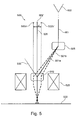
- Fig. 5 shows an optical system 500 similar to the system described in the published patent application US 2006 / 0151711 .
- a primary-electron beam 501 from an emitter (not shown) is bent (changes direction) as it passes through a magnetic beam deflection coil 505, and changes direction again as it passes through a further magnetic beam deflection coil 515.
- the primary-electron beam 501 is then focused onto a sample 530 by an objective lens 525 (e.g. electrostatic and/or magnetic focussing lens) defining an optical axis 526.
- an objective lens 525 e.g. electrostatic and/or magnetic focussing lens
- a signal electron beam 535 resulting from an interaction of the primary beam 501 with the sample 530, then travels along the opposite direction.
- the signal electron beam 535 is bent as it passes through the further magnetic-beam separator deflection coil 515 and is thereby separated from the primary beam 501. Then, the signal beam 535 is guided to a detector (not shown).
- the deflection of the primary beam 501 due to coil 505 is the same in magnitude and opposite in sign as its deflection due to coil 515.
- the purpose of this arrangement is to allow a column which is vertically aligned, and hence allows vertically aligned optical elements in the regions upstream the deflection coil 505 and downstream of the deflector 515, despite the fact that the deflection coil 515 deflects the beam.
- the double deflection further has the effect of displacing the beam 501 as shown in Fig. 5 .
- the beam 501 seems to emerge from a virtual source 502' that is displaced with respect to the real source 502.
- the objective lens 525 is arranged such that the virtual source 502' lies on the optical axis 526 defined by the objective lens 525.
- Fig. 5 in addition to the primary beam 501 as represented by the main energy beam portion of the beam 501, a beam portion 501a with lower energy, and a beam portion 501b with higher energy than the mean energy is shown. Also for the beam portions 501a and 501b, the deflection due to coil 505 is the same in magnitude and opposite in sign as the deflection due to coil 515. However, the lower-energy beam portion 501a is deflected by both coils 505, 515 to a larger degree, and is therefore finally displaced more than the main-energy beam portion 501.
- the virtual source 502a' of the lower-energy beam portion 501a is displaced with respect to the virtual source 502' of the main beam portion.
- the higher-energy beam portion 501b is deflected by both coils 505, 515 to a lesser degree, and is therefore displaced less than the main-energy beam portion 501.
- the virtual source 502b' of the higher-energy beam portion 501b is displaced with respect to the virtual source 502' of the main beam portion.
- a beam containing the beam portions 501a and 501b seems to come from a line-like virtual source of width d instead of a point-like virtual source, and the beam hitting on the specimen is correspondingly widened in the deflection direction (i.e. the direction orthogonal to the optical axis 526 in the drawing plane of Fig. 5 ).
- This widening limits the available resolution in the deflection direction.
- a chromatic aberration i.e. a variation, with respect to the beam energy, of the location at which the primary beam hits the specimen.
- a first-order chromatic aberration of the electron beam apparatus is defined as the first derivative, with respect to the beam energy, of the location at which the primary beam hits the specimen, at the main beam energy.
- the location of the beam hitting the specimen is energy (momentum) dependent, causing the beam to be widened in the deflection direction perpendicular to the optical axis.
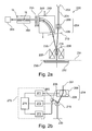
- Fig. 1 shows an electron beam device according to a first embodiment of the invention.
- the electron beam device 100 includes a beam emitter 102 for emitting a primary electron beam 101, and an objective electron lens 125 for focusing the primary electron beam 101 onto a specimen 130, the objective lens defining an optical axis 126.
- a specimen includes, but is not limited to, semiconductor wafers, semiconductor workpieces, and other workpieces such as optical blanks, memory disks and the like. Embodiments of the invention may be applied to any workpiece on which material is deposited or which are structured.
- a specimen includes a flat surface to be structured or on which layers are deposited, an opposing surface, an edge, and typically a bevel.
- the objective lens 125 is a final focusing lens.
- the lens i.e. elements generating a focusing field for focusing the beam on the specimen and the focusing field itself
- the lens body the body containing these elements and possibly further related elements in a body having a lens bore for the electron beam.
- the term "lens" may also refer to the lens body.
- the lens may be a multiple-element lens such as a combined electrostatic-magnetic lens provided in a common lens housing. In Fig. 1 , only the magnetic portion of the combined electrostatic-magnetic lens is shown.
- the lens may be e.g. an electrostatic lens.
- the objective lens may be arranged at a distance of less than 100 mm or even less than 50 mm, and / or of less than 1 ⁇ 4 of the total primary beam length, from the specimen (specimen plane).
- the electron beam device 100 further includes a beam separator 115.
- the beam separator 115 is a purely magnetic beam separator.
- the beam separator 115 may be immersed in the body of the objective lens 125, e.g. located essentially ("essentially" means by more than half of the beam separator's length along the optical axis) within or downstream of the body, in particular at least partially within or downstream a bore of the objective lens 125, see Fig. 4 .
- the beam separator 115 may be located upstream of the objective lens 125.
- the beam separator 115 may be located directly upstream of the objective lens 125, i.e.
- a beam scanner such as a magnetic and / or electrostatic scanner may be arranged, along the beam path, between beam separator 115 and the objective lens 125.
- the magnetic beam separator 115 has a first dispersion.
- an element having a dispersion means that the element is adapted for acting on the electron beam according to the dispersion (dispersion relation), i.e. to deflect electrons of the beam by a deflection angle which depends on the electron energy or momentum.
- the first dispersion is anisotropic and defines a first deflection direction (direction within the drawing plane of Fig. 1 and orthogonal to the optical axis 126).
- the magnetic beam separator 115 is able to separate a signal electron beam 135 from the primary electron beam 101 (according to their different momentum or direction).
- signal electrons are defined as electrons travelling in an essentially opposite direction from the primary beam electrons, and the signal electrons may, in particular, include secondary electrons, auger electrons, and/or backscattered electrons.
- the beam separator 115 has a deflection coil for deflecting the primary electron beam 101.
- the deflection coil generates a transverse magnetic field for separating the signal electron beam 135 from the primary electron beam 101.
- the transverse field is orthogonal to the drawing plane of Fig. 1 .
- the electrons of the beams 101 and 135 traverse the magnetic field, they experience a force which is dependent upon the electron velocity (Lorentz force law). Since the primary electrons (beam 101) and signal electrons (beam 135) are essentially traveling in opposite directions, the force acting upon the two beams will be opposite in direction when traveling through the transverse magnetic field. Thus, the primary beam 101 and the secondary beam 135 are both deflected, by angles of opposite sign.
- the magnetic beam separator is a purely magnetic beam separator, i.e. it includes a magnetic element (e.g. magnetic coil or dipole element) as the only deflecting element, and no other, e.g. electrostatic, deflecting component.
- the electron beam device 100 is configured such that no electrostatic deflecting field acts on the primary beam 101 at the location of the beam separator 115 (as would be the case, for example, for a Wien filter).
- Using a purely magnetic deflector as the beam separator 115 has the advantage that the region inside the objective lens 125 can be kept free of parts that require intensive servicing. For example, electrostatic deflectors are prone to contamination and therefore require frequent servicing.
- a dispersion compensation element 104 described below, upstream of the beam separator 115, the latter can have a simple construction which does not require serviceable parts. This allows the beam separator 115 to be immersed in the body of the objective lens, which is difficult to access for servicing.
- the beam separator 115 is a deflector which induces a deflection angle which smoothly depends on the beam energy of the primary beam 101. Hence, the deflector is different from an energy filter allowing only electrons above a threshold energy to pass. As a further general aspect, the beam separator 115 deflects the primary electrons to a direction which is essentially along the optical axis defined by the objective lens.
- the electron beam device 100 further includes a dispersion compensation element 104.
- the dispersion compensation element 104 is arranged upstream, along the primary electron beam 101, of the beam separator 115.
- the secondary electrons do not reach the dispersion compensation element 104, in other words the dispersion compensation element 104 is arranged outside a signal electron beam 135 path of the electron beam device 100, such that it influences only the primary beam but not directly the signal electron beam 135.
- the dispersion compensation element 104 has a second dispersion, i.e. the dispersion compensation element is adapted for acting on the primary beam according to the second dispersion.
- the second dispersion is anisotropic defining a second deflection direction parallel (which includes the case antiparallel) to the first deflection direction, defined by the beam separator 115.
- the labels "first”, "second” do not imply any order along the beam path.
- the dispersion compensation element 104 allows adjusting the second dispersion. More particularly, the second dispersion can be adjusted such that the second dispersion substantially compensates the first dispersion.
- This compensation of the first dispersion is to be understood as follows: By adjusting the second dispersion of the dispersion compensation element 104, it is possible to adjust the first derivative, with respect to the beam energy, of the beam location at which the primary beam 101 electrons hit the specimen 130 (defined as the first-order chromatic aberration). The first dispersion is compensated when this first derivative is brought to zero (or, in practice, close to zero i.e. the beam widening is at least considerably reduced, compared to the case for which the second dispersion is not adjusted).
- the dispersion compensation element 104 allows adjusting the second dispersion such that the above-mentioned first derivative of the beam location is brought to zero or close to zero. In consequence, the mean beam width can be reduced considerably.
- the dispersion compensation element may also be controlled in such a way that this pre-determined energy-dependence is achieved.
- the adjustment of the second dispersion can be performed automatically by a dispersion compensation controller (as shown e.g. in Fig. 2b ) or by manual adjustment.
- the adjustment can also be done e.g. during setup of the apparatus, and the adjusted dispersion is then hard-wired into the control of the dispersion compensation element 104.
- the dispersion compensation element 104 is adapted for adjusting the second dispersion independently of an inclination angle of the primary beam 101 downstream of the dispersion compensation element 104.
- the dispersion compensation element 104 is adapted for adjusting the second dispersion without substantially affecting the inclination angle of the primary beam 101 path downstream of the dispersion compensation element 104.
- the inclination angle is defined relative to the optical axis 126.
- the dispersion compensation element 104 may be adapted for adjusting the second dispersion relation independently of the entire path of the primary beam 101 from the emitter to the specimen 130; i.e. the dispersion compensation element acts in a dispersive manner without affecting significantly the entire primary beam 101 path (this is the case in Figs. 1 , 2 , 3a and 3b ).
- the apparatus may be adapted for the functions described herein e.g. by a controller that is programmed, hard-wired, or in any other manner adapted for achieving that function.
- the controller may be provided as an electronic, in particular as a digital controller, but also e.g. as an electrical circuit or by mechanical coupling elements, to achieve the desired function.
- the path-independent adjustment is possible only for primary beam electrons of a particular energy at or near the main beam energy: Due to the second dispersion, the inclination angle of the primary beam path downstream of the dispersion compensation element will depend on the beam energy. "Without substantially affecting the inclination angle” therefore means that there is an energy at or near the main beam energy of beam 101 (e.g. an energy away from the mean beam energy by less than five times or even less than two times of the beam energy width), at which energy the inclination angle is not affected noticeably when adjusting the second dispersion by a small amount (e.g. to linear order).
- a small amount e.g. to linear order
- the primary-electron beam 101 from the emitter 102 passes through the dispersion compensation element 104 and undergoes the second dispersion.
- the primary beam 101 may be deflected (as shown in Fig. 1 ).
- the primary beam 101 leaves the dispersion compensation element 104 at an inclined angle with respect to the optical axis 126, and is received in the beam separator 115 at the inclined angle.
- the inclination angle of the primary electron beam 101 directly upstream of the beam separator 115 is generally non-zero but less than 10°.
- the primary-electron beam 101 then passes through the magnetic beam separator 115 and is deflected therein, such that the primary beam 101 becomes essentially parallel to or even coinciding with the optical axis downstream of the beam separator 115. At the same time, the primary beam 101 undergoes the first dispersion.
- the primary-electron beam 101 is then focused by the objective lens 125 to strike the sample 130, such as a semiconductor wafer. Because the first dispersion has been compensated by the second dispersion, the beam 101 hits the sample 130 with high resolution.
- the secondary-electron beam 135 resulting from the interaction of the primary beam 101 with the sample 130 passes again, but in opposite direction, through the objective lens 125 and is deflected as it passes through the magnetic beam separator 115 and is thereby separated from the primary beam 101 (as described above).
- the secondary-electron beam 135, after having been separated from the primary beam 101, is then guided to an electron detector (by elements not shown in Fig. 1 ).
- the device of Fig. 1 has the further advantage that it allows a high-intensity beam, and therefore enables fast inspection at high throughput at a good signal to noise ratio: Namely, because the beam separator 115 is immersed in the body of the objective lens 125, the common path for the primary beam 101 and the secondary beam 135 is very short. Thereby, inter-beam electron-electron interactions (i.e. interactions between electrons of the primary beam 101 and electrons of the secondary beam 135) are reduced.
- the common beam path was made shorter. Namely, by shortening the path at which such head-on collisions can occur (i.e. the common beam path between the primary beam 101 and the signal electron beam 135), the beam intensity can be increased at a given level of tolerated head-on collisions.
- the short common beam path can be achieved by the beam separator 115 being immersed in the body of the objective lens 125, or being arranged directly upstream or downstream of the objective lens.
- the distance of the beam separator 115 from a specimen plane 131 can be made less than 100mm, in some embodiments even less than 70 mm or even 50 mm, such that the common path of the primary and signal electrons is less than 100 mm, 70 mm or 50 mm.
- the common path of the primary and signal electrons may be made shorter than 25% of the total primary beam length, i.e. the primary beam length from the electron source to the specimen.
- the apparatus of Fig. 1 allows a minimized collision length of primary and secondary beam, that enables high-intensity operation at high spatial resolution.
- the apparatus of Fig. 1 may have additional elements such as a condenser lens e.g. upstream the objective lens and in particular upstream of the dispersion compensation element.
- a condenser lens e.g. upstream the objective lens and in particular upstream of the dispersion compensation element.
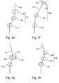
- the dispersion compensation element 204 includes a magnetic coil (magnetic deflector) 205 and an electric (electrostatic) deflector 206, both deflectors 205 and 206 being adapted to deflect the beam 201 within the same deflection plane (here, the deflection plane, i.e. the plane within which the beam is deflected, is the drawing plane of Fig. 2a ). Further, the deflectors 205 and 206 are connected to a control apparatus 270 which is described in more detail below. In Fig.
- the total deflection D of the dispersion compensation element 204 is chosen to have equal magnitude and opposite sign as the deflection of the beam separator 215. This allows a vertical column, and hence vertically aligned optical elements, in the regions upstream the deflector 205 and downstream of the deflector 215.
- Fig. 2a includes some additional elements of the electron beam apparatus 200 (these elements may also, but do not need to be present in the embodiment of Fig. 1 ): Namely, the apparatus 200 of Fig. 2a includes a plate 210 having openings for the primary and the signal beam, and a collecting arrangement (elements arranged along the beam path of the signal beam 235). Further, the apparatus 200 has a specimen receiver 232 defining a specimen plane 231 at which the specimen 230 interacts with the electron beam 201.
- the primary-electron beam 201 travels as described with respect to Fig. 1 , and additionally passes through an opening in a plate 210.
- the resulting signal electron beam 235 after having been separated from the primary beam 201 by the beam separator 215, passes through a further opening in the plate 210 and is then guided to an electron detector 265 as described e.g. in US patent No. 7,335,894 (see Fig. 5 and col. 9 line 57 to col. 10 line 56 thereof).
- the signal electron beam 235 could alternatively be guided to the detector in any other manner.
- the electron beam device 200 further includes a specimen receiver 232 for receiving the specimen 230.
- the specimen receiver 232 defines a specimen plane 231 at which the specimen 230 interacts with the electron beam 201 during operation of the electron beam device 200.
- the electron beam device 200 of Fig. 2a may include still further elements not shown in Fig. 2a .
- the electron beam device 200 may include an energy filter for the primary electron beam 201, a beam boost electrode for accelerating the electron beam 201, and/or a scan system for scanning the beam 201 over the specimen.
- the scan system may include e.g. electrostatic deflection plates or magnetic deflection coils or a combination thereof.
- the scan system may include between 4 and 16 electrostatic deflection plates, e.g. 8 electrostatic deflection plates.
- the scan system may include at least two deflection coils (at least one coil for each scanning direction in the specimen plane).
- the deflection system is generally located downstream of the beam separator 215, i.e. inside or downstream of the objective lens 225.
- Fig. 2b shows the apparatus of Fig. 2a (with some optional elements omitted), and additionally a controller 270.
- the controller is adapted for adjusting the second dispersion independently of the inclination angle of the primary beam 201 downstream of the dispersion compensation element 204, such that the dispersion compensation element 204 acts on the primary beam according to the second dispersion such as to substantially compensate the first dispersion.
- the controller 270 has a dispersion compensation controller 271 connected to the dispersion compensation element 204, a beam separation controller 272 connected to the beam separation element 215, an optional beam analyser 273 connected to the electron detector 265, and a main controller unit 274 connected to the controllers 271, 272 and 273.
- the controller 270 is adapted for operation according to a predetermined beam separation deflection of the beam separation element 215, as follows:
- the main controller unit 274 feeds the predetermined beam separation deflection to the beam separation controller 272, and the beam separation controller 272 controls the beam separation element 215 to cause the beams 201 and 235 to be deflected by the predetermined beam separation deflection, thereby causing a first dispersion of the beam 201.
- the main controller unit 274 determines an appropriate second dispersion which compensates for the first dispersion, and transmits the second dispersion to the dispersion compensation controller 271.
- the dispersion compensation controller then causes the dispersion compensation element 204 to achieve the second dispersion.
- the main controller unit 274 may determine the appropriate second dispersion by various methods. For example, according to a feedback control loop, the beam analyser 273 receives image information from the electron detector 265 and generates an image quality signal therefrom (e.g. a spot size indicative signal). The main controller unit 274 then receives the image quality signal from the beam analyser 273 for various second dispersions and then selects the appropriate second dispersion according to the image quality signal. Alternatively, the main controller unit 274 may calculate an appropriate second dispersion based on a model of the beam such as the model illustrated in Fig. 1 . The criterion should be that the first-order chromatic aberration of the electron beam 201 hitting the specimen should be zero. Also, the main controller unit 274 may use take the appropriate second dispersion from a stored table of appropriate values for various parameters.
- the controller 270 of Fig. 2b is adapted for the embodiment of Fig. 2a and 2b . However, it is clear that by including some variations, the controller 270 may be adapted for any other embodiments shown or claimed herein, e.g. the embodiments of Figs. 3a to 3h .
- the dispersion compensation element of the embodiments of Fig.1 , Fig. 2a or Fig. 2b is suitable for adjusting the dispersion such that the total dispersion (first-order chromatic aberration) is zero
- the apparatus does not necessarily need to operate in this manner. Instead, it may be sufficient to implement some approximate control of the dispersion compensation element, such that the total dispersion is sufficiently close to zero for the desired resolution.
- a beam having a particular total dispersion may be desired for some applications.
- the dispersion of the dispersion compensation element 104 can be adjusted to provide the desired total dispersion (which may be zero or non-zero).
- Figs. 3a to 3h possible realizations of the dispersion compensation element 104 are illustrated. Any of these elements can be used in place of the dispersion compensation element 104 / 204 of Fig. 1 or of Fig. 2 .
- the contribution of one of the deflectors, d1 can be varied.
- the deflections d1 and d2 can have the same sign or have opposite sign. In this manner, the dispersion can be varied by changing the value of d1, while the total deflection D is held constant.
- the total deflection D may be zero or have a finite value.
- the two deflectors of the dispersion compensation element 104 are selected to have respective dispersions which depend on their deflection in a different manner.
- one of the deflectors may be an electric deflector and the other may be a magnetic deflector.
- the sum of their dispersions depends on the individual contributions d1 and d2 to the total deflection D, the total deflection D being kept constant.
- the dispersion compensation element 104 can also include three or more deflectors.
- the dispersion compensation element 104 allows adjusting the second dispersion such that the second dispersion substantially compensates the first dispersion, without need to worry about a change in the beam inclination further downstream of the dispersion compensation element 104.
- the second dispersion is also adjustable independently of the entire beam path of the primary beam 101 (e.g. also independently of its displacement) downstream of the dispersion compensation element 104.
- the dispersion compensation element 104 of Fig. 3a corresponds to that of Fig. 2 , and the corresponding description of Fig. 2 also applies to Fig. 3a .
- the dispersion compensation element 104 includes a magnetic deflector 105 and an electrostatic deflector 106.
- the deflectors 105, 106 are controlled to give a nonzero total deflection D that is opposite to the deflection of the beam separation element 115.
- the dispersion compensation element 104 of Fig. 3b has similar elements as the one of Fig. 3a , and the description of Fig. 3a also applies to Fig. 3b unless specified otherwise.
- the deflectors 105, 106 are controlled to give a zero total deflection D.
- the dispersion compensation element 104 is a Wien filter.
- the beam 101 upstream of the beam separator 115 in Fig. 3b is thus inclined with respect to the optical axis.
- the beam source 102 and any other electron-optical elements upstream of the beam separator 135 are adapted for the inclined beam 101.
- Fig. 3c shows an arrangement of dispersion compensation element 104 and beam separator 115 which is similar to that of Fig. 3a , but in which the dispersion compensation element 104 is tilted with respect to the optical axis. More precisely, the dispersion compensation element 104 is tilted such that its axis 104a has a non-zero angle with respect to the incoming beam 101. This angle is smaller than the deflection angle, i.e. the angle between the incoming beam and the outgoing beam from the dispersion compensation element 104. In particular, this angle may be half of the deflection angle.
- the axis 104a may be defined, for example, as being perpendicular to a main magnetic field as well as to a main electric field of the dispersion compensation element.
- Fig. 3d shows an arrangement of dispersion compensation element 104 and beam separator 115 which is similar to that of Fig. 3b , but in which the dispersion compensation element (Wien filter) 104 is tilted with respect to the optical axis. More precisely, the dispersion compensation element 104 is tilted such that its axis 104a is parallel to the incoming beam 101. In contrast, the beam separator 115 (see Fig. 1 ) is parallel to the optical axis.
- the magnetic deflector 105 and the electrostatic deflector 106 are spatially separated from one another along the primary beam 101.
- the beam Due to the spatial separation of the deflectors 105, 106, the beam is displaced, due to a similar effect as described with reference to Fig. 5 . As a result, this displacement can be seen as an additional contribution to the second dispersion (dependence of the location of the beam 101 hitting the specimen on beam energy) of the dispersion correction element 104. This additional contribution may be taken into account when the deflections d1 and d2 are adjusted such that in the end the total dispersion is zero. When the deflectors 105, 106 are displaced only by a small distance, the additional contribution to the second dispersion may also be neglected.
- the electrostatic deflector 106 is arranged upstream, along the primary beam 101 path, of the magnetic deflector 105.
- the electrostatic deflector 106 may be arranged downstream of the magnetic deflector 105.
- the deflectors 105, 106 are controlled to provide deflections in the same direction.
- the deflectors 105, 106 may be controlled to provide deflections in opposite direction such that the deflection of deflectors 105, 106 partially or fully cancel each other.
- the dispersion compensation element 104 contains a magnetic deflector 105 and a beam-tilter 107.
- the magnetic deflector 105 can also be replaced by an electrostatic deflector or another type of deflector.
- the beam-tilter 107 has the effect of tilting the incoming electron beam 101 as seen by the magnetic deflector 105, or in other words of tilting the inclination angle of the virtual image of the beam source 102 as seen by the magnetic deflector 105.
- the beam tilter 107 can, in principle, be implemented as a mechanical beam tilter for swiveling the beam source about a center, the center being preferably located at the center of the deflector 105.
- the beam-tilter 107 has no dispersion, thus the total dispersion of the dispersion compensation element 104 equals the dispersion of the magnetic deflector 105.
- the beam tilter 107 can be implemented by a deflector 106 as shown e.g. in Fig. 3a or 3c , or by a series of deflectors (electrostatic, magnetic, some other deflector, or combination thereof).
- the physical position of the beam source 102 may remain unchanged, and only the virtual source position is changed.
- the deflector of the beam tilter 107 is preferably of different type than the deflector 105, because otherwise the net dispersion of the beam tilter 107 and the deflector 105 would largely cancel so that the dispersion cannot be adjusted easily.
- the beam-tilter 107 can include a combination of a mechanical beam-tilter and of one or more deflector(s) (electric or magnetic or combination thereof). Then, the angle of the beam tilter 107 and the deflection due to the deflector 105 can be adjusted together such that the inclination angle of the primary beam 101 downstream of the deflector 105 is unchanged.
- the second dispersion is adjusted. In particular, the second dispersion can be adjusted such that the second dispersion substantially compensates the first dispersion.
- Fig. 3g shows a similar arrangement as that of Fig. 3a , but in which the beam 101 directly upstream the dispersion compensation element 104 is inclined with respect to the optical axis.
- the inclination may be adjustable as in Fig. 3f , but does not need to be adjustable as long as the dispersion is adjustable.
- an apparatus with non-adjustable inclination but adjustable dispersion is described.
- the beam upstream the dispersion compensation element 104 and the beam downstream the beam separator 115 are not parallel to each other.
- the deflection angles of the dispersion compensation element 104 and of the beam separator 115 of Fig. 3g have different absolute values.
- the beam apparatus may be adapted for a particular rated beam energy.
- the inclination angle of the beam 101 directly upstream the dispersion compensation element 104 can be chosen such that for zero electric field of the electrostatic deflector 106 and at the rated beam energy, the total first-order chromatic aberration of the beam 101 is zero.
- This inclination may be found by a numerical simulation of the beam path of beam 101.
- the inclination may be found by tuning an apparatus with adjustable inclination (such as the apparatus of Fig. 3f ), until the chromatic aberration vanishes.
- the electrodes can be arranged relatively far away from the beam 101, where they are less prone to contamination.
- Fig. 3h shows a further variation of the apparatus of Fig. 3g , and the above description of Fig. 3g also applies to Fig. 3h .
- the electric and magnetic deflectors 105, 106 of the dispersion compensation element 104 are overlapping each other (as also shown above in Fig. 3a ), in Fig. 3h they are located at different positions along the beam path of the electron beam 101 (as also shown above in Fig. 3b ).
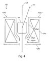
- the objective lens 125 and the arrangement of the beam separation element 115 inside the objective lens 125 are described.
- the objective lens is a beam focusing lens for focusing the primary beam 101 on the specimen 130, more specifically a final focusing lens.
- the objective lens 125 may also be adapted for demagnifying the crossover of the electron beam 101.
- the objective lens 125 (more precisely, the lens body) shown in Fig. 4 is a compound lens having a magnetic lens element 125c.
- an upper (upstream) electrode 125a and a lower (downstream) electrode 125b are provided as part of the objective lens body.
- the upper electrode 125a is at a higher potential than the electrode 125b.
- the upper electrode 125a has, in direction from upstream to downstream, an electrode plate 125a1 with an opening, a first cylindrical portion 125a2, a tapered portion 125a3, and a second cylindrical portion 125a4.
- the upper electrode 125a is arranged concentrically to the optical axis 126.
- the inner diameter of the first cylindrical portion 125a2 is larger than the inner diameter of the second cylindrical portion 125a4, and the tapered portion 125a3 connects these two portions 125a2 and 125a4.
- the electrodes 125a, 125b may be biased in such a way that the lower electrode decelerates and thereby focuses the beam.
- the magnetic lens element 125c serves for adjusting the focusing effect of the lens. In a purely electrostatic lens, the magnetic lens element 125c may be replaced by a third electrostatic electrode.
- the beam separation element 115 is placed at least partially inside the lens 125, i.e. there is a cross-sectional plane perpendicular to the optical axis 126 containing both a portion of the lens 125 (magnetic lens element 125c) and a portion of the beam separation element 115.
- the beam separation element 115 is placed inside the magnetic lens surrounding a liner tube. Further, the beam separation element 115 is placed more towards the entry (most upstream portion) than towards the exit (most downstream portion) of the lens body of lens 125.
- the beam separation element 115 is placed at least partially inside a bore of the lens and/or of the upper electrode 125a.
- the beam separation element 115 may be placed at least partially inside the first cylindrical portion 125a2 of the upper electrode 125a.
- the objective lens 125 is shown as a compound electric-magnetic lens, but it may also be a different type of lens such as an electrostatic lens.
- the lens may have one or more focusing electrode(s) for focusing the primary beam.
- the focusing electrode may at the same time serve for decelerating the beam to a predetermined energy.
- the focusing electrode may further be supplemented by an adjustment electrode and/or another adjustment arrangement (such as a magnetic arrangement 125c as shown in Fig. 4 ) for adjusting and fine-tuning the focus.
- a further electrode may be controlled to have specimen potential..
- the beam separator may in any case be immersed into the lens body as shown in Fig. 4 , or directly upstream of the objective lens, i.e.
- a beam scanner may be provided between the beam separator and the objective lens downstream of the beam separator.
- the beam scanner may be provided as the only element therebetween.
- the beam scanner may be a magnetic or electrostatic scanner.
- the scanner may at the same time have additional functionality such as in the case of an electrostatic scanner whose electrostatic octupol element also provides a stigmator field.
- the beam separator is generally arranged such that its magnetic deflection field does substantially not overlap with the electrostatic focusing field of the objective lens.
- the objective lens 125 may be a double-focusing sector unit including a sector (a quadrupole unit, and cylinder lens or side plates) for focusing in a first dimension and a sector for focusing in a second direction.
- the objective lens 125 may alternatively also be an Einzel-lens or any other type of lens.
- the beam separator 115 is located in the bore of the objective lens 125, but outside a region of substantial focusing electrical field of the objective lens 125.Thereby, a substantial superposition of magnetic deflection field of the beam separator 115 and of electric focusing field of the lens 125 are avoided.
- a scanning unit (not shown) may be provided.
- the scanning unit may be positioned either within the lens 125 (e.g. downstream of the beam separator 115) or further downstream of the lens 125, i.e. positioned between the lens and the specimen.
- the structure for guiding the signal electron beam to the beam detector can be arbitrarily varied.
- the structure includes focusing and filtering optics for the signal electron beam which have no effect on the primary electron beam.
- the electron beam device can include a plurality of columns, each column including a respective beam source and the other elements as described herein, such as some or all elements shown in Fig. 1 .
- the electron beam apparatus can include further electron-optical elements such as a scanning arrangement downstream of the electron objective lens.
- the beam separator is a deflector for deflecting the primary electron beam.
- the beam separator is a purely magnetic deflector, i.e. it contains no other, e.g. electrostatic, deflecting component, and in particular includes a magnetic dipole element as the only deflecting element. Hence, no electric deflector is included (unlike e.g. a Wien filter element).
- the beam separator is adapted for receiving the primary beam as an inclined beam with respect to the optical axis, and for deflecting the primary beam such that the primary beam exits the beam separator essentially in parallel to the optical axis.
- the electron beam device further includes a specimen receiver for receiving a specimen, the specimen receiver defining a specimen plane at which the specimen interacts with the electron beam during operation of the electron beam device.
- the distance of the beam separator from the specimen plane is less than 100 mm, less than 70 mm, or even less than 50 mm, and/or less than 1 ⁇ 4 of the total beam length of the primary beam. In this manner, the common path of the primary and secondary electrons is enabled to be less than this distance.
- the inclination angle of the primary electron beam directly upstream of the beam separator is less than 10°.
- the beam separator is placed at least partially in an upstream half portion of the lens.
- the distance of the optical lens from the specimen plane is less than 70 mm, or even less than 50 mm, and/or less than 1 ⁇ 4 of the total beam length of the primary beam.
- the dispersion compensation element is adapted for inclining the electron beam by less than 20°, less than 12°, or even less than 10°.
- the beam separator is adapted for inclining the electron beam by less than 20°, less than 12°, or even less than 10°.
- the lens has an electrode having a cylindrical upstream portion of larger inner diameter and a cylindrical downstream portion of smaller inner diameter, and the beam separator is placed at least partially inside the upstream portion.
- the beam separation element and / or the dispersion compensation element are provided at a cross-over-free beam path position of the primary beam, i.e. at a position at which there is no cross-over of the beam during operation of the apparatus.
- the dispersion compensation element and the beam separator are adapted for deflecting the electron beam within the same plane.
- the dispersion compensation element is adapted for adjusting the second dispersion relation independently of a path of the primary beam, in particular for adjusting it independently of the entire path from the emitter to the specimen. Then, the dispersion compensation element acts in a dispersive manner substantially without affecting the entire primary beam path, for electrons of a main velocity.
- the dispersion compensation element includes a first deflector and a second deflector, wherein the first deflector and the second deflector have mutually different dispersion characteristics. This is e.g. the case for an electric deflector and a magnetic deflector.
- the dispersion characteristics of both deflectors are different from one another if there is at least one deflection angle magnitude for which the dispersion of the first deflector is different from that of the second deflector, for a main energy of the electron beam.
- the deflectors are adapted for deflecting the electron beam in mutually opposite directions such that the deflection cancels each other but the dispersions do not cancel each other.
- the electron beam device is adapted for controlling the first and second deflectors to have substantially opposite deflection angles.
- a dispersion compensation element controller is adapted for supplying a first deflection power to the first deflector and a second deflection power to the second deflector such that the deflection angles of the first and the second deflector are substantially opposite one another. "substantially opposite” means opposite for a main energy beam portion of the primary beam.
- a dispersion compensation element controller is adapted for controlling the first and second deflectors to have deflection angles that add up to a pre-determined deflection angle, the pre-determined deflection angle being equal in magnitude but opposite to the deflection angle of the beam separator.
- the dispersion compensation element is arranged outside a secondary electron path of the electron beam device, i.e. in a primary-electron-beam-only region.
- the first dispersion is anisotropic defining a first deflection direction orthogonal to the optical axis
- the second dispersion is also anisotropic defining a second deflection direction parallel to the first deflection direction (herein, "parallel” also includes the case antiparallel).
- the electron beam device includes a dispersion compensation controller adapted for adjusting the second dispersion substantially independently of an inclination angle of the primary beam downstream of the dispersion compensation element, such that the dispersion compensation element acts on the primary beam according to the second dispersion such as to substantially compensate the first dispersion.
- the magnetic beam separator is adapted for acting outside a region of a substantial electric field of the objective lens.
Landscapes
- Chemical & Material Sciences (AREA)
- Analytical Chemistry (AREA)
- Analysing Materials By The Use Of Radiation (AREA)
- Electron Beam Exposure (AREA)
- Electron Sources, Ion Sources (AREA)
Description
- Aspects of the invention relate to an electron beam device, e.g. for imaging or for manipulating a specimen, and a method of operating the same. More particularly, aspects of the invention relate to an electron beam device including a beam emitter; an objective electron lens; and a beam separator for separating a signal electron beam from the primary electron beam.
- Charged particle beam apparatuses have many functions in a plurality of industrial fields, including, but not limited to, inspection of semiconductor devices during manufacturing, exposure systems for lithography, detecting devices and testing systems. Thus, there is a high demand for structuring and inspecting specimens within the micrometer and nanometer scale.
- In particular, semiconductor technologies have created a high demand for structuring and probing specimens within the nanometer scale. Micrometer and nanometer scale process control, inspection or structuring, is often done with electron beams. Probing or structuring is often performed with electron beams which are generated and focused in electron beam devices. Examples of electron beam devices are electron microscopes, in particular scanning electron microscopes (SEM), or electron beam pattern generators. Electron beams offer superior spatial resolution compared to photon beams, due to their short wavelengths at comparable particle energy.
- For semiconductor manufacturing, throughput can be a significant limitation in tools for scanning a geometry in its entirety. Assuming a SEM resolution of 1 nm, a 10 mm2 die contains 10E14 pixels. Accordingly, for covering the entire layout, a fast inspection architecture is desired. For achieving high throughput at a desired signal to noise ratio (SNR), it is desired to have an electron beam device with a high electron beam intensity.
- However, at high electron beam intensity the interaction between electrons of the electron beam have an increasing effect on the beam. Due to the electron-electron interactions, the energy and spatial resolution of the beam is decreased. Therefore, measures to mitigate the electron-electron interactions of the beam have been devised, such as a broadening of the primary electron beam. However, there is still a need to reduce the effect of electron-electron interactions even further.
-
US 5,422,486 describes a scanning electron beam device with a two-stage Wien filter and an electrostatic reflector. The primary electron beam is not deflected by the Wien filter but merely spread (dispersed), with opposing and mutually compensating spreading occurring in the two stages. Further,JP 2004/342341 US 2004/227081 describes an electron beam apparatus having an orthogonal electric-magnetic field generator for separating the secondary signal. Further,WO 00/36630 - In light of the above, the present invention intends to provide an improved electron beam device, and an improved method of operating an electron beam device.
- The object is solved by the electron beam device according to independent claim 1, and by the method according to independent claim 13. Further advantages, features, aspects and details of the invention are evident from the dependent claims, the description and the drawings.
- According to one embodiment, an electron beam device includes a beam emitter for emitting a primary electron beam; an objective electron lens for focusing the primary electron beam onto a specimen, the objective lens defining an optical axis; a beam separator having a first dispersion for separating a signal electron beam from the primary electron beam, wherein the beam separator is a purely magnetic deflector including a magnetic element as the only deflecting element; and a dispersion compensation element having a second dispersion. The dispersion compensation element is adapted for adjusting the second dispersion independently of an inclination angle of the primary beam downstream of the dispersion compensation element, such that the second dispersion substantially compensates the first dispersion. The dispersion compensation element is arranged upstream, along the primary electron beam, of the beam separator.
- According to another embodiment, a method of operating an electron beam device includes: Generating a primary electron beam; focusing, by means of an objective electron lens, the primary electron beam onto a specimen; generating a signal electron beam by interaction of the primary beam with the specimen; acting, by a beam separator, on the primary electron beam and on the signal electron beam according to a first dispersion thereby separating the signal electron beam from the primary electron beam; and adjusting a second dispersion of a dispersion compensation element, independently of an inclination angle of the primary beam downstream of the dispersion compensation element, such that the dispersion compensation element acts on the primary beam according to the second dispersion such as to substantially compensate the first dispersion. The beam separator is a purely magnetic deflector and deflects the primary electron beam by a magnetic element as the only deflecting element.
- Embodiments are also directed to methods by which the described apparatus operates. The methods include method steps for carrying out every function of the apparatus. Further, embodiments are also directed to a beam apparatus having a controller adapted for carrying out any of the method steps described herein.
- Some of the above indicated and other more detailed aspects of the invention will be described in the following description and partially illustrated with reference to the figures. Therein:
-
FIG. 1 shows a schematic side view of an electron beam apparatus according to a first embodiment; -
FIGS. 2a and 2b show schematic side views of an electron beam apparatus according to a further embodiment; -
FIGS. 3a to 3h show schematic side views of respective dispersion compensation elements of electron beam apparatuses according to further embodiments; -
FIG. 4 shows a schematic side view of an objective lens body and a beam separation element immersed therein; and -
FIG. 5 shows a schematic side view of an electron beam apparatus according to a comparative example. - In the following passages different aspects of the invention are defined in more detail. Without limiting the scope of the present application, the electron beam apparatus might be adapted for inspection or lithography, such as a scanning electron microscope (SEM) or the like.
- So that the advantages of the embodiments can be better appreciated, first an illustrative example will be described with reference to
Fig. 5. Fig. 5 shows anoptical system 500 similar to the system described in the published patent applicationUS 2006 / 0151711 . In theoptical system 500, a primary-electron beam 501 from an emitter (not shown) is bent (changes direction) as it passes through a magneticbeam deflection coil 505, and changes direction again as it passes through a further magneticbeam deflection coil 515. The primary-electron beam 501 is then focused onto asample 530 by an objective lens 525 (e.g. electrostatic and/or magnetic focussing lens) defining anoptical axis 526. Asignal electron beam 535, resulting from an interaction of theprimary beam 501 with thesample 530, then travels along the opposite direction. Thesignal electron beam 535 is bent as it passes through the further magnetic-beamseparator deflection coil 515 and is thereby separated from theprimary beam 501. Then, thesignal beam 535 is guided to a detector (not shown). - In the system of
Fig. 5 , the deflection of theprimary beam 501 due tocoil 505 is the same in magnitude and opposite in sign as its deflection due tocoil 515. The purpose of this arrangement is to allow a column which is vertically aligned, and hence allows vertically aligned optical elements in the regions upstream thedeflection coil 505 and downstream of thedeflector 515, despite the fact that thedeflection coil 515 deflects the beam. The double deflection further has the effect of displacing thebeam 501 as shown inFig. 5 . Thus, when entering theobjective lens 525, thebeam 501 seems to emerge from a virtual source 502' that is displaced with respect to thereal source 502. Theobjective lens 525 is arranged such that the virtual source 502' lies on theoptical axis 526 defined by theobjective lens 525. - However, by the arrangement of
Fig. 5 the image is blurred due to dispersion: InFig. 5 , in addition to theprimary beam 501 as represented by the main energy beam portion of thebeam 501, a beam portion 501a with lower energy, and a beam portion 501b with higher energy than the mean energy is shown. Also for the beam portions 501a and 501b, the deflection due tocoil 505 is the same in magnitude and opposite in sign as the deflection due tocoil 515. However, the lower-energy beam portion 501a is deflected by bothcoils energy beam portion 501. Hence, thevirtual source 502a' of the lower-energy beam portion 501a is displaced with respect to the virtual source 502' of the main beam portion. Similarly, the higher-energy beam portion 501b is deflected by bothcoils energy beam portion 501. Hence, thevirtual source 502b' of the higher-energy beam portion 501b is displaced with respect to the virtual source 502' of the main beam portion. As a result, a beam containing the beam portions 501a and 501b seems to come from a line-like virtual source of width d instead of a point-like virtual source, and the beam hitting on the specimen is correspondingly widened in the deflection direction (i.e. the direction orthogonal to theoptical axis 526 in the drawing plane ofFig. 5 ). This widening limits the available resolution in the deflection direction. Thus, there is a chromatic aberration, i.e. a variation, with respect to the beam energy, of the location at which the primary beam hits the specimen. Here, a first-order chromatic aberration of the electron beam apparatus is defined as the first derivative, with respect to the beam energy, of the location at which the primary beam hits the specimen, at the main beam energy. - In summary, with the apparatus of
Fig. 5 the location of the beam hitting the specimen is energy (momentum) dependent, causing the beam to be widened in the deflection direction perpendicular to the optical axis. - In the following, embodiments of the invention are described which reduce the disadvantage mentioned with respect to the above-described illustrative example of
Fig. 5 . Within the following description of the drawings, reference numbers having the same last two digits refer to the same or similar components. Generally, only the differences with respect to the individual embodiments are described, so that the description of any one embodiment can also be applied to another embodiment, unless otherwise stated. In particular any feature indicated as being preferred or advantageous is optional. Also, such a feature indicated as being preferred or advantageous may be combined with any other feature or features indicated as being preferred or advantageous. -
Fig. 1 shows an electron beam device according to a first embodiment of the invention. Theelectron beam device 100 includes abeam emitter 102 for emitting aprimary electron beam 101, and anobjective electron lens 125 for focusing theprimary electron beam 101 onto aspecimen 130, the objective lens defining anoptical axis 126. A specimen, as referred to herein, includes, but is not limited to, semiconductor wafers, semiconductor workpieces, and other workpieces such as optical blanks, memory disks and the like. Embodiments of the invention may be applied to any workpiece on which material is deposited or which are structured. A specimen includes a flat surface to be structured or on which layers are deposited, an opposing surface, an edge, and typically a bevel. Theobjective lens 125 is a final focusing lens. In the following, no clear distinction is made between the lens (i.e. elements generating a focusing field for focusing the beam on the specimen and the focusing field itself) and the lens body (the body containing these elements and possibly further related elements in a body having a lens bore for the electron beam). As used in the following, the term "lens" may also refer to the lens body. The lens may be a multiple-element lens such as a combined electrostatic-magnetic lens provided in a common lens housing. InFig. 1 , only the magnetic portion of the combined electrostatic-magnetic lens is shown. Alternatively, the lens may be e.g. an electrostatic lens. As a general aspect independent of the shown embodiment, the objective lens may be arranged at a distance of less than 100 mm or even less than 50 mm, and / or of less than ¼ of the total primary beam length, from the specimen (specimen plane). - The
electron beam device 100 further includes abeam separator 115. Thebeam separator 115 is a purely magnetic beam separator. Thebeam separator 115 may be immersed in the body of theobjective lens 125, e.g. located essentially ("essentially" means by more than half of the beam separator's length along the optical axis) within or downstream of the body, in particular at least partially within or downstream a bore of theobjective lens 125, seeFig. 4 . Also, especially in the case of an electrostatic lens, thebeam separator 115 may be located upstream of theobjective lens 125. Thebeam separator 115 may be located directly upstream of theobjective lens 125, i.e. with essentially no other electron-optical element between thebeam separator 115 and theobjective lens 125, along theelectron beam path 101. Alternatively, e.g. a beam scanner, such as a magnetic and / or electrostatic scanner may be arranged, along the beam path, betweenbeam separator 115 and theobjective lens 125. - The
magnetic beam separator 115 has a first dispersion. Here, an element having a dispersion (or dispersion relation) means that the element is adapted for acting on the electron beam according to the dispersion (dispersion relation), i.e. to deflect electrons of the beam by a deflection angle which depends on the electron energy or momentum. The first dispersion is anisotropic and defines a first deflection direction (direction within the drawing plane ofFig. 1 and orthogonal to the optical axis 126). - Due to the first dispersion, the
magnetic beam separator 115 is able to separate asignal electron beam 135 from the primary electron beam 101 (according to their different momentum or direction). Here, signal electrons are defined as electrons travelling in an essentially opposite direction from the primary beam electrons, and the signal electrons may, in particular, include secondary electrons, auger electrons, and/or backscattered electrons. - In more detail, here, the
beam separator 115 has a deflection coil for deflecting theprimary electron beam 101. The deflection coil generates a transverse magnetic field for separating thesignal electron beam 135 from theprimary electron beam 101. The transverse field is orthogonal to the drawing plane ofFig. 1 . When the electrons of thebeams primary beam 101 and thesecondary beam 135 are both deflected, by angles of opposite sign. - The magnetic beam separator is a purely magnetic beam separator, i.e. it includes a magnetic element (e.g. magnetic coil or dipole element) as the only deflecting element, and no other, e.g. electrostatic, deflecting component. Thus, the
electron beam device 100 is configured such that no electrostatic deflecting field acts on theprimary beam 101 at the location of the beam separator 115 (as would be the case, for example, for a Wien filter). - Using a purely magnetic deflector as the
beam separator 115 has the advantage that the region inside theobjective lens 125 can be kept free of parts that require intensive servicing. For example, electrostatic deflectors are prone to contamination and therefore require frequent servicing. By having adispersion compensation element 104, described below, upstream of thebeam separator 115, the latter can have a simple construction which does not require serviceable parts. This allows thebeam separator 115 to be immersed in the body of the objective lens, which is difficult to access for servicing. - As a further general aspect, the
beam separator 115 is a deflector which induces a deflection angle which smoothly depends on the beam energy of theprimary beam 101. Hence, the deflector is different from an energy filter allowing only electrons above a threshold energy to pass. As a further general aspect, thebeam separator 115 deflects the primary electrons to a direction which is essentially along the optical axis defined by the objective lens. - The
electron beam device 100 further includes adispersion compensation element 104. Thedispersion compensation element 104 is arranged upstream, along theprimary electron beam 101, of thebeam separator 115. As an aspect of the invention independently of the shown embodiment, the secondary electrons do not reach thedispersion compensation element 104, in other words thedispersion compensation element 104 is arranged outside asignal electron beam 135 path of theelectron beam device 100, such that it influences only the primary beam but not directly thesignal electron beam 135. Some possible realizations of thedispersion compensation element 104 are described in more detail further below with reference toFigs. 2 and3a-3h . Thedispersion compensation element 104 ofFig. 1 may be realized according to any one of these Figures, e.g. according toFig. 3a described further below. - Continuing the description of
Fig. 1 , thedispersion compensation element 104 has a second dispersion, i.e. the dispersion compensation element is adapted for acting on the primary beam according to the second dispersion. The second dispersion is anisotropic defining a second deflection direction parallel (which includes the case antiparallel) to the first deflection direction, defined by thebeam separator 115. Herein, the labels "first", "second" do not imply any order along the beam path. - Further, the
dispersion compensation element 104 allows adjusting the second dispersion. More particularly, the second dispersion can be adjusted such that the second dispersion substantially compensates the first dispersion. This compensation of the first dispersion is to be understood as follows: By adjusting the second dispersion of thedispersion compensation element 104, it is possible to adjust the first derivative, with respect to the beam energy, of the beam location at which theprimary beam 101 electrons hit the specimen 130 (defined as the first-order chromatic aberration). The first dispersion is compensated when this first derivative is brought to zero (or, in practice, close to zero i.e. the beam widening is at least considerably reduced, compared to the case for which the second dispersion is not adjusted). Thus, thedispersion compensation element 104 allows adjusting the second dispersion such that the above-mentioned first derivative of the beam location is brought to zero or close to zero. In consequence, the mean beam width can be reduced considerably. - While the adjustment of the second dispersion allows compensating the first dispersion such as to give a zero or substantially reduced chromatic aberration, there may be applications in which some pre-determined energy-dependence of the electron beam hitting the specimen is actually desired. In this case the dispersion compensation element may also be controlled in such a way that this pre-determined energy-dependence is achieved.
- The adjustment of the second dispersion can be performed automatically by a dispersion compensation controller (as shown e.g. in
Fig. 2b ) or by manual adjustment. The adjustment can also be done e.g. during setup of the apparatus, and the adjusted dispersion is then hard-wired into the control of thedispersion compensation element 104. - Further, the
dispersion compensation element 104 is adapted for adjusting the second dispersion independently of an inclination angle of theprimary beam 101 downstream of thedispersion compensation element 104. In other words, thedispersion compensation element 104 is adapted for adjusting the second dispersion without substantially affecting the inclination angle of theprimary beam 101 path downstream of thedispersion compensation element 104. The inclination angle is defined relative to theoptical axis 126. - The
dispersion compensation element 104 may be adapted for adjusting the second dispersion relation independently of the entire path of theprimary beam 101 from the emitter to thespecimen 130; i.e. the dispersion compensation element acts in a dispersive manner without affecting significantly the entireprimary beam 101 path (this is the case inFigs. 1 ,2 ,3a and 3b ). - Within this description, the apparatus may be adapted for the functions described herein e.g. by a controller that is programmed, hard-wired, or in any other manner adapted for achieving that function. The controller may be provided as an electronic, in particular as a digital controller, but also e.g. as an electrical circuit or by mechanical coupling elements, to achieve the desired function.
- Clearly, the path-independent adjustment is possible only for primary beam electrons of a particular energy at or near the main beam energy: Due to the second dispersion, the inclination angle of the primary beam path downstream of the dispersion compensation element will depend on the beam energy. "Without substantially affecting the inclination angle" therefore means that there is an energy at or near the main beam energy of beam 101 (e.g. an energy away from the mean beam energy by less than five times or even less than two times of the beam energy width), at which energy the inclination angle is not affected noticeably when adjusting the second dispersion by a small amount (e.g. to linear order).
- Thus, in the
electron beam device 100 ofFig. 1 , the primary-electron beam 101 from theemitter 102 passes through thedispersion compensation element 104 and undergoes the second dispersion. At the same time, theprimary beam 101 may be deflected (as shown inFig. 1 ). Theprimary beam 101 leaves thedispersion compensation element 104 at an inclined angle with respect to theoptical axis 126, and is received in thebeam separator 115 at the inclined angle. The inclination angle of theprimary electron beam 101 directly upstream of thebeam separator 115 is generally non-zero but less than 10°. - The primary-
electron beam 101 then passes through themagnetic beam separator 115 and is deflected therein, such that theprimary beam 101 becomes essentially parallel to or even coinciding with the optical axis downstream of thebeam separator 115. At the same time, theprimary beam 101 undergoes the first dispersion. The primary-electron beam 101 is then focused by theobjective lens 125 to strike thesample 130, such as a semiconductor wafer. Because the first dispersion has been compensated by the second dispersion, thebeam 101 hits thesample 130 with high resolution. - The secondary-
electron beam 135 resulting from the interaction of theprimary beam 101 with thesample 130 passes again, but in opposite direction, through theobjective lens 125 and is deflected as it passes through themagnetic beam separator 115 and is thereby separated from the primary beam 101 (as described above). The secondary-electron beam 135, after having been separated from theprimary beam 101, is then guided to an electron detector (by elements not shown inFig. 1 ). - The device of
Fig. 1 has the further advantage that it allows a high-intensity beam, and therefore enables fast inspection at high throughput at a good signal to noise ratio: Namely, because thebeam separator 115 is immersed in the body of theobjective lens 125, the common path for theprimary beam 101 and thesecondary beam 135 is very short. Thereby, inter-beam electron-electron interactions (i.e. interactions between electrons of theprimary beam 101 and electrons of the secondary beam 135) are reduced. - The effect of such inter-beam interactions has previously not been taken much into account. However, the inventors have found indirect but convincing evidence indicating that such inter-beam interactions have a significant negative effect on image quality: Namely, in an apparatus such as the one shown in
Fig. 1 and at large beam intensities and energies, an extra contribution to the blurring of theprimary beam 101 was found. This extra contribution can be explained by the fact that the inter-beam interactions involve head-on electron-electron collisions. These collisions cause unwanted beam widening and are detrimental to the attainable resolution. The head-on collisions are therefore expected to be particularly detrimental at high beam energies and intensities. - This extra contribution to blurring was reduced when the common beam path was made shorter. Namely, by shortening the path at which such head-on collisions can occur (i.e. the common beam path between the
primary beam 101 and the signal electron beam 135), the beam intensity can be increased at a given level of tolerated head-on collisions. The short common beam path can be achieved by thebeam separator 115 being immersed in the body of theobjective lens 125, or being arranged directly upstream or downstream of the objective lens. Thereby, the distance of thebeam separator 115 from a specimen plane 131 (plane at which the electron beam hits the specimen 130) can be made less than 100mm, in some embodiments even less than 70 mm or even 50 mm, such that the common path of the primary and signal electrons is less than 100 mm, 70 mm or 50 mm. Also, the common path of the primary and signal electrons may be made shorter than 25% of the total primary beam length, i.e. the primary beam length from the electron source to the specimen. The high-intensity beam thus obtainable enables a fast inspection at high throughput and at a good signal to noise ratio. - In summary, the apparatus of
Fig. 1 allows a minimized collision length of primary and secondary beam, that enables high-intensity operation at high spatial resolution. - The apparatus of
Fig. 1 may have additional elements such as a condenser lens e.g. upstream the objective lens and in particular upstream of the dispersion compensation element. - With reference to
Fig. 2 and3a-d , further embodiments will now be described. The more general description ofFig. 1 also applies to these further embodiments. - In the electron beam apparatus (e.g. SEM) 200 of
Fig. 2 , thedispersion compensation element 204 includes a magnetic coil (magnetic deflector) 205 and an electric (electrostatic)deflector 206, bothdeflectors beam 201 within the same deflection plane (here, the deflection plane, i.e. the plane within which the beam is deflected, is the drawing plane ofFig. 2a ). Further, thedeflectors control apparatus 270 which is described in more detail below. InFig. 2 , the total deflection D of thedispersion compensation element 204 is chosen to have equal magnitude and opposite sign as the deflection of thebeam separator 215. This allows a vertical column, and hence vertically aligned optical elements, in the regions upstream thedeflector 205 and downstream of thedeflector 215. - Further to the description of
Fig. 1 ,Fig. 2a includes some additional elements of the electron beam apparatus 200 (these elements may also, but do not need to be present in the embodiment ofFig. 1 ): Namely, theapparatus 200 ofFig. 2a includes aplate 210 having openings for the primary and the signal beam, and a collecting arrangement (elements arranged along the beam path of the signal beam 235). Further, theapparatus 200 has aspecimen receiver 232 defining aspecimen plane 231 at which thespecimen 230 interacts with theelectron beam 201. - In the
electron beam apparatus 200 ofFig. 2a , the primary-electron beam 201 travels as described with respect toFig. 1 , and additionally passes through an opening in aplate 210. - The resulting
signal electron beam 235, after having been separated from theprimary beam 201 by thebeam separator 215, passes through a further opening in theplate 210 and is then guided to anelectron detector 265 as described e.g. inUS patent No. 7,335,894 (seeFig. 5 and col. 9 line 57 to col. 10 line 56 thereof). Thesignal electron beam 235 could alternatively be guided to the detector in any other manner. - The
electron beam device 200 further includes aspecimen receiver 232 for receiving thespecimen 230. Thespecimen receiver 232 defines aspecimen plane 231 at which thespecimen 230 interacts with theelectron beam 201 during operation of theelectron beam device 200. - The
electron beam device 200 ofFig. 2a may include still further elements not shown inFig. 2a . For example, theelectron beam device 200 may include an energy filter for theprimary electron beam 201, a beam boost electrode for accelerating theelectron beam 201, and/or a scan system for scanning thebeam 201 over the specimen. The scan system may include e.g. electrostatic deflection plates or magnetic deflection coils or a combination thereof. For example. the scan system may include between 4 and 16 electrostatic deflection plates, e.g. 8 electrostatic deflection plates. Also, the scan system may include at least two deflection coils (at least one coil for each scanning direction in the specimen plane). The deflection system is generally located downstream of thebeam separator 215, i.e. inside or downstream of theobjective lens 225. -
Fig. 2b shows the apparatus ofFig. 2a (with some optional elements omitted), and additionally acontroller 270. The controller is adapted for adjusting the second dispersion independently of the inclination angle of theprimary beam 201 downstream of thedispersion compensation element 204, such that thedispersion compensation element 204 acts on the primary beam according to the second dispersion such as to substantially compensate the first dispersion. - To this purpose, the
controller 270 has adispersion compensation controller 271 connected to thedispersion compensation element 204, abeam separation controller 272 connected to thebeam separation element 215, anoptional beam analyser 273 connected to theelectron detector 265, and amain controller unit 274 connected to thecontrollers - As a general aspect independent of the shown embodiment, the
dispersion compensation controller 271 is connected to thedispersion compensation element 204 and programmed, hard-wired or in any other way adapted for adjusting the second dispersion independently of an inclination angle of theprimary beam 201 downstream of thedispersion compensation element 204. So, in the example shown inFig. 2b , thedispersion compensation controller 271 is adapted for adjusting the deflections d1, d2 of thedeflectors - According to one mode of operation, the
controller 270 is adapted for operation according to a predetermined beam separation deflection of thebeam separation element 215, as follows: Themain controller unit 274 feeds the predetermined beam separation deflection to thebeam separation controller 272, and thebeam separation controller 272 controls thebeam separation element 215 to cause thebeams beam 201. Themain controller unit 274 then determines an appropriate second dispersion which compensates for the first dispersion, and transmits the second dispersion to thedispersion compensation controller 271. The dispersion compensation controller then causes thedispersion compensation element 204 to achieve the second dispersion. - The
main controller unit 274 may determine the appropriate second dispersion by various methods. For example, according to a feedback control loop, thebeam analyser 273 receives image information from theelectron detector 265 and generates an image quality signal therefrom (e.g. a spot size indicative signal). Themain controller unit 274 then receives the image quality signal from thebeam analyser 273 for various second dispersions and then selects the appropriate second dispersion according to the image quality signal. Alternatively, themain controller unit 274 may calculate an appropriate second dispersion based on a model of the beam such as the model illustrated inFig. 1 . The criterion should be that the first-order chromatic aberration of theelectron beam 201 hitting the specimen should be zero. Also, themain controller unit 274 may use take the appropriate second dispersion from a stored table of appropriate values for various parameters. - The
controller 270 ofFig. 2b is adapted for the embodiment ofFig. 2a and 2b . However, it is clear that by including some variations, thecontroller 270 may be adapted for any other embodiments shown or claimed herein, e.g. the embodiments ofFigs. 3a to 3h . - Further, while the dispersion compensation element of the embodiments of
Fig.1 ,Fig. 2a or Fig. 2b is suitable for adjusting the dispersion such that the total dispersion (first-order chromatic aberration) is zero, the apparatus does not necessarily need to operate in this manner. Instead, it may be sufficient to implement some approximate control of the dispersion compensation element, such that the total dispersion is sufficiently close to zero for the desired resolution. Alternatively, a beam having a particular total dispersion may be desired for some applications. In this case, the dispersion of thedispersion compensation element 104 can be adjusted to provide the desired total dispersion (which may be zero or non-zero). - In
Figs. 3a to 3h , possible realizations of thedispersion compensation element 104 are illustrated. Any of these elements can be used in place of thedispersion compensation element 104 / 204 ofFig. 1 or ofFig. 2 . - Generally, the
dispersion compensation element 104 may be equipped with two deflectors, e.g. an electric and a magnetic deflector, whose individual deflections (individual contributions, denoted as d1 and d2, respectively, to the total deflection ofbeam 101 at or near the main beam energy) are controlled such that the total deflection D = d1 + d2 stays constant. Thus, the contribution of one of the deflectors, d1, can be varied. The other deflector is then controlled to provide the remaining deflection d2 = D - d1. The deflections d1 and d2 can have the same sign or have opposite sign. In this manner, the dispersion can be varied by changing the value of d1, while the total deflection D is held constant. The total deflection D may be zero or have a finite value. - Further, the two deflectors of the
dispersion compensation element 104 are selected to have respective dispersions which depend on their deflection in a different manner. For example, one of the deflectors may be an electric deflector and the other may be a magnetic deflector. In this case, the sum of their dispersions depends on the individual contributions d1 and d2 to the total deflection D, the total deflection D being kept constant. Similarly, thedispersion compensation element 104 can also include three or more deflectors. - Thus, the
dispersion compensation element 104 allows adjusting the second dispersion such that the second dispersion substantially compensates the first dispersion, without need to worry about a change in the beam inclination further downstream of thedispersion compensation element 104. In some embodiments, the second dispersion is also adjustable independently of the entire beam path of the primary beam 101 (e.g. also independently of its displacement) downstream of thedispersion compensation element 104. - The
dispersion compensation element 104 ofFig. 3a corresponds to that ofFig. 2 , and the corresponding description ofFig. 2 also applies toFig. 3a . InFig. 3a , thedispersion compensation element 104 includes amagnetic deflector 105 and anelectrostatic deflector 106. Thedeflectors beam separation element 115. - The
dispersion compensation element 104 ofFig. 3b has similar elements as the one ofFig. 3a , and the description ofFig. 3a also applies toFig. 3b unless specified otherwise. However, different fromFig. 3a , thedeflectors dispersion compensation element 104 is a Wien filter. The dispersion of the Wien filter can be adjusted by tuning the individual deflections d1 and d2 simultaneously so that always D = d1+d2 = 0. - The
beam 101 upstream of thebeam separator 115 inFig. 3b is thus inclined with respect to the optical axis. Correspondingly thebeam source 102 and any other electron-optical elements upstream of thebeam separator 135 are adapted for theinclined beam 101. -
Fig. 3c shows an arrangement ofdispersion compensation element 104 andbeam separator 115 which is similar to that ofFig. 3a , but in which thedispersion compensation element 104 is tilted with respect to the optical axis. More precisely, thedispersion compensation element 104 is tilted such that itsaxis 104a has a non-zero angle with respect to theincoming beam 101. This angle is smaller than the deflection angle, i.e. the angle between the incoming beam and the outgoing beam from thedispersion compensation element 104. In particular, this angle may be half of the deflection angle. Theaxis 104a may be defined, for example, as being perpendicular to a main magnetic field as well as to a main electric field of the dispersion compensation element. -
Fig. 3d shows an arrangement ofdispersion compensation element 104 andbeam separator 115 which is similar to that ofFig. 3b , but in which the dispersion compensation element (Wien filter) 104 is tilted with respect to the optical axis. More precisely, thedispersion compensation element 104 is tilted such that itsaxis 104a is parallel to theincoming beam 101. In contrast, the beam separator 115 (seeFig. 1 ) is parallel to the optical axis. - In
dispersion compensation element 104 ofFig. 3e , themagnetic deflector 105 and theelectrostatic deflector 106 are spatially separated from one another along theprimary beam 101. Thedeflectors Fig. 3a ). - Due to the spatial separation of the
deflectors Fig. 5 . As a result, this displacement can be seen as an additional contribution to the second dispersion (dependence of the location of thebeam 101 hitting the specimen on beam energy) of thedispersion correction element 104. This additional contribution may be taken into account when the deflections d1 and d2 are adjusted such that in the end the total dispersion is zero. When thedeflectors - In
Fig. 3e , theelectrostatic deflector 106 is arranged upstream, along theprimary beam 101 path, of themagnetic deflector 105. In an alternative variant, theelectrostatic deflector 106 may be arranged downstream of themagnetic deflector 105. Further, inFig. 3e , thedeflectors deflectors deflectors - In
dispersion compensation element 104 ofFig. 3f , thedispersion compensation element 104 contains amagnetic deflector 105 and a beam-tilter 107. Alternatively, themagnetic deflector 105 can also be replaced by an electrostatic deflector or another type of deflector. - The beam-
tilter 107 has the effect of tilting theincoming electron beam 101 as seen by themagnetic deflector 105, or in other words of tilting the inclination angle of the virtual image of thebeam source 102 as seen by themagnetic deflector 105. - The
beam tilter 107 can, in principle, be implemented as a mechanical beam tilter for swiveling the beam source about a center, the center being preferably located at the center of thedeflector 105. In the case of a mechanical beam-tilter 107, the beam-tilter has no dispersion, thus the total dispersion of thedispersion compensation element 104 equals the dispersion of themagnetic deflector 105. - Alternatively, the
beam tilter 107 can be implemented by adeflector 106 as shown e.g. inFig. 3a or 3c , or by a series of deflectors (electrostatic, magnetic, some other deflector, or combination thereof). In this case, the physical position of thebeam source 102 may remain unchanged, and only the virtual source position is changed. The deflector of thebeam tilter 107 is preferably of different type than thedeflector 105, because otherwise the net dispersion of thebeam tilter 107 and thedeflector 105 would largely cancel so that the dispersion cannot be adjusted easily. - Also, the beam-
tilter 107 can include a combination of a mechanical beam-tilter and of one or more deflector(s) (electric or magnetic or combination thereof). Then, the angle of thebeam tilter 107 and the deflection due to thedeflector 105 can be adjusted together such that the inclination angle of theprimary beam 101 downstream of thedeflector 105 is unchanged. Hereby, the second dispersion is adjusted. In particular, the second dispersion can be adjusted such that the second dispersion substantially compensates the first dispersion. -
Fig. 3g shows a similar arrangement as that ofFig. 3a , but in which thebeam 101 directly upstream thedispersion compensation element 104 is inclined with respect to the optical axis. The inclination may be adjustable as inFig. 3f , but does not need to be adjustable as long as the dispersion is adjustable. In the following, an apparatus with non-adjustable inclination but adjustable dispersion is described. - In
Fig. 3g the beam upstream thedispersion compensation element 104 and the beam downstream thebeam separator 115 are not parallel to each other. In other words, the deflection angles of thedispersion compensation element 104 and of thebeam separator 115 ofFig. 3g have different absolute values. - The beam apparatus may be adapted for a particular rated beam energy. In this case, the inclination angle of the
beam 101 directly upstream thedispersion compensation element 104 can be chosen such that for zero electric field of theelectrostatic deflector 106 and at the rated beam energy, the total first-order chromatic aberration of thebeam 101 is zero. This inclination may be found by a numerical simulation of the beam path ofbeam 101. Alternatively, the inclination may be found by tuning an apparatus with adjustable inclination (such as the apparatus ofFig. 3f ), until the chromatic aberration vanishes. - With this inclination, the dispersion of the
dispersion compensation element 104 can be adjusted as inFig. 3a , by simultaneous adjustment of thedeflectors beam 101, where they are less prone to contamination. -
Fig. 3h shows a further variation of the apparatus ofFig. 3g , and the above description ofFig. 3g also applies toFig. 3h . However, while inFig. 3g the electric andmagnetic deflectors dispersion compensation element 104 are overlapping each other (as also shown above inFig. 3a ), inFig. 3h they are located at different positions along the beam path of the electron beam 101 (as also shown above inFig. 3b ). - In the following, with reference to
Fig. 4 , theobjective lens 125 and the arrangement of thebeam separation element 115 inside theobjective lens 125 are described. Generally, the objective lens is a beam focusing lens for focusing theprimary beam 101 on thespecimen 130, more specifically a final focusing lens. Theobjective lens 125 may also be adapted for demagnifying the crossover of theelectron beam 101. - The objective lens 125 (more precisely, the lens body) shown in
Fig. 4 is a compound lens having amagnetic lens element 125c. In addition, an upper (upstream)electrode 125a and a lower (downstream)electrode 125b are provided as part of the objective lens body. Theupper electrode 125a is at a higher potential than theelectrode 125b. Theupper electrode 125a has, in direction from upstream to downstream, an electrode plate 125a1 with an opening, a first cylindrical portion 125a2, a tapered portion 125a3, and a second cylindrical portion 125a4. Theupper electrode 125a is arranged concentrically to theoptical axis 126. The inner diameter of the first cylindrical portion 125a2 is larger than the inner diameter of the second cylindrical portion 125a4, and the tapered portion 125a3 connects these two portions 125a2 and 125a4. - The
electrodes magnetic lens element 125c serves for adjusting the focusing effect of the lens. In a purely electrostatic lens, themagnetic lens element 125c may be replaced by a third electrostatic electrode. - The
beam separation element 115 is placed at least partially inside thelens 125, i.e. there is a cross-sectional plane perpendicular to theoptical axis 126 containing both a portion of the lens 125 (magnetic lens element 125c) and a portion of thebeam separation element 115. Alternatively stated, thebeam separation element 115 is placed inside the magnetic lens surrounding a liner tube. Further, thebeam separation element 115 is placed more towards the entry (most upstream portion) than towards the exit (most downstream portion) of the lens body oflens 125. Generally and not limited to the embodiment ofFig. 4 , thebeam separation element 115 is placed at least partially inside a bore of the lens and/or of theupper electrode 125a. For the electrode shown inFig. 4 , thebeam separation element 115 may be placed at least partially inside the first cylindrical portion 125a2 of theupper electrode 125a. - The
objective lens 125 is shown as a compound electric-magnetic lens, but it may also be a different type of lens such as an electrostatic lens. In any case, the lens may have one or more focusing electrode(s) for focusing the primary beam. The focusing electrode may at the same time serve for decelerating the beam to a predetermined energy. The focusing electrode may further be supplemented by an adjustment electrode and/or another adjustment arrangement (such as amagnetic arrangement 125c as shown inFig. 4 ) for adjusting and fine-tuning the focus. A further electrode may be controlled to have specimen potential.. The beam separator may in any case be immersed into the lens body as shown inFig. 4 , or directly upstream of the objective lens, i.e. with no other beam-optical element inbetween. Also, a beam scanner may be provided between the beam separator and the objective lens downstream of the beam separator. In particular, the beam scanner may be provided as the only element therebetween. The beam scanner may be a magnetic or electrostatic scanner. Also, the scanner may at the same time have additional functionality such as in the case of an electrostatic scanner whose electrostatic octupol element also provides a stigmator field. Also, the beam separator is generally arranged such that its magnetic deflection field does substantially not overlap with the electrostatic focusing field of the objective lens. - The
objective lens 125 may be a double-focusing sector unit including a sector (a quadrupole unit, and cylinder lens or side plates) for focusing in a first dimension and a sector for focusing in a second direction. Theobjective lens 125 may alternatively also be an Einzel-lens or any other type of lens. - According to a general aspect, the
beam separator 115 is located in the bore of theobjective lens 125, but outside a region of substantial focusing electrical field of the objective lens 125.Thereby, a substantial superposition of magnetic deflection field of thebeam separator 115 and of electric focusing field of thelens 125 are avoided. - Further, a scanning unit (not shown) may be provided. The scanning unit may be positioned either within the lens 125 (e.g. downstream of the beam separator 115) or further downstream of the
lens 125, i.e. positioned between the lens and the specimen. - The above embodiments can be varied in a number of further ways. For example, the structure for guiding the signal electron beam to the beam detector can be arbitrarily varied. Generally, the structure includes focusing and filtering optics for the signal electron beam which have no effect on the primary electron beam.
- Further, the electron beam device can include a plurality of columns, each column including a respective beam source and the other elements as described herein, such as some or all elements shown in
Fig. 1 . Also, the electron beam apparatus can include further electron-optical elements such as a scanning arrangement downstream of the electron objective lens. - In the following, some further general aspects of the invention are described. Any of these aspects may be combined with any other aspect or embodiment described herein.
- The beam separator is a deflector for deflecting the primary electron beam. The beam separator is a purely magnetic deflector, i.e. it contains no other, e.g. electrostatic, deflecting component, and in particular includes a magnetic dipole element as the only deflecting element. Hence, no electric deflector is included (unlike e.g. a Wien filter element).
- According to a further aspect, the beam separator is adapted for receiving the primary beam as an inclined beam with respect to the optical axis, and for deflecting the primary beam such that the primary beam exits the beam separator essentially in parallel to the optical axis.
- According to a further aspect, The electron beam device further includes a specimen receiver for receiving a specimen, the specimen receiver defining a specimen plane at which the specimen interacts with the electron beam during operation of the electron beam device. Further, the distance of the beam separator from the specimen plane is less than 100 mm, less than 70 mm, or even less than 50 mm, and/or less than ¼ of the total beam length of the primary beam. In this manner, the common path of the primary and secondary electrons is enabled to be less than this distance. According to a further aspect, the inclination angle of the primary electron beam directly upstream of the beam separator is less than 10°. According to a further aspect, the beam separator is placed at least partially in an upstream half portion of the lens. According to a further aspect, the distance of the optical lens from the specimen plane is less than 70 mm, or even less than 50 mm, and/or less than ¼ of the total beam length of the primary beam.
- According to a further aspect, the dispersion compensation element is adapted for inclining the electron beam by less than 20°, less than 12°, or even less than 10°. Also, according to a yet further aspect, the beam separator is adapted for inclining the electron beam by less than 20°, less than 12°, or even less than 10°.
- According to a further aspect, the lens has an electrode having a cylindrical upstream portion of larger inner diameter and a cylindrical downstream portion of smaller inner diameter, and the beam separator is placed at least partially inside the upstream portion.
- According to a further aspect, the beam separation element and / or the dispersion compensation element are provided at a cross-over-free beam path position of the primary beam, i.e. at a position at which there is no cross-over of the beam during operation of the apparatus.
- According to a further aspect, the dispersion compensation element and the beam separator are adapted for deflecting the electron beam within the same plane.
- According to a further aspect, the dispersion compensation element is adapted for adjusting the second dispersion relation independently of a path of the primary beam, in particular for adjusting it independently of the entire path from the emitter to the specimen. Then, the dispersion compensation element acts in a dispersive manner substantially without affecting the entire primary beam path, for electrons of a main velocity. According to a further aspect, the dispersion compensation element includes a first deflector and a second deflector, wherein the first deflector and the second deflector have mutually different dispersion characteristics. This is e.g. the case for an electric deflector and a magnetic deflector. More specifically, the dispersion characteristics of both deflectors are different from one another if there is at least one deflection angle magnitude for which the dispersion of the first deflector is different from that of the second deflector, for a main energy of the electron beam. According to a further aspect, the deflectors are adapted for deflecting the electron beam in mutually opposite directions such that the deflection cancels each other but the dispersions do not cancel each other.
- According to a further aspect, the electron beam device is adapted for controlling the first and second deflectors to have substantially opposite deflection angles. Thus, a dispersion compensation element controller is adapted for supplying a first deflection power to the first deflector and a second deflection power to the second deflector such that the deflection angles of the first and the second deflector are substantially opposite one another. "substantially opposite" means opposite for a main energy beam portion of the primary beam.
- According to a further aspect, a dispersion compensation element controller is adapted for controlling the first and second deflectors to have deflection angles that add up to a pre-determined deflection angle, the pre-determined deflection angle being equal in magnitude but opposite to the deflection angle of the beam separator.
- According to a further aspect, the dispersion compensation element is arranged outside a secondary electron path of the electron beam device, i.e. in a primary-electron-beam-only region.
- According to a further aspect, the first dispersion is anisotropic defining a first deflection direction orthogonal to the optical axis, and the second dispersion is also anisotropic defining a second deflection direction parallel to the first deflection direction (herein, "parallel" also includes the case antiparallel).
- According to a further aspect, the electron beam device includes a dispersion compensation controller adapted for adjusting the second dispersion substantially independently of an inclination angle of the primary beam downstream of the dispersion compensation element, such that the dispersion compensation element acts on the primary beam according to the second dispersion such as to substantially compensate the first dispersion. According to a further aspect, the magnetic beam separator is adapted for acting outside a region of a substantial electric field of the objective lens.
- While the foregoing is directed to embodiments of the invention, further embodiments of the invention may be devised without departing from the basic scope thereof, and the scope thereof is determined by the claims that follow.
Claims (13)
- An electron beam device (100, 200), comprising:a beam emitter (102, 202) for emitting a primary electron beam (101, 201);an objective electron lens (125, 225) for focusing the primary electron beam (101, 201) onto a specimen (130, 230), the objective lens defining an optical axis (126, 226);a beam separator (115, 215) having a first dispersion for separating a signal electron beam (135, 235) from the primary electron beam (101, 201), anda dispersion compensation element (104, 204) having a second dispersion, the dispersion compensation element being adapted for adjusting the second dispersion independently of an inclination angle of the primary beam (101, 201) downstream of the dispersion compensation element (104, 204), such that the second dispersion substantially compensates the first dispersion, whereinthe dispersion compensation element (104, 204) is arranged upstream, along the primary electron beam (101, 201), of the beam separator (115, 215),characterised in that the beam separator is a purely magnetic deflector including a magnetic element as the only deflecting element.
- The electron beam device according to claim 1, wherein the beam separator (115) is adapted for receiving the primary beam (101) as an inclined beam with respect to the optical axis (126), and for deflecting the primary beam such that the primary beam downstream of the beam separator (115) is essentially parallel to the optical axis.
- The electron beam device according to any one of the preceding claims, further comprising a specimen receiver (132) for receiving a specimen (130), the specimen receiver (132) defining a specimen plane (131) at which the specimen (130) interacts with the electron beam (101) during operation of the electron beam device (100), wherein the distance of the beam separator (115) from the specimen plane (131) is less than 1/4 of the primary beam length.
- The electron beam device according to any one of the preceding claims, wherein the dispersion compensation element (104) is adapted for adjusting the second dispersion relation independently of a path of the primary beam.
- The electron beam device according to any one of the preceding claims, wherein the dispersion compensation element (104) comprises a first deflector (105) and a second deflector (106), wherein the first deflector (105) and the second deflector (106) have mutually different dispersion characteristics.
- The electron beam device according to claim 5, wherein the first deflector (105) is a magnetic deflector, and the second deflector (106) is an electrostatic deflector.
- The electron beam device according to claim 5 or 6, adapted for controlling the first and second deflectors (105, 106) to have deflection angles of opposite sign.
- The electron beam device according to any one of claims 5 to 6, adapted for controlling the first and second deflectors (105, 106) to have deflection angles that add up to a pre-determined deflection angle, the pre-determined deflection angle being equal in magnitude but opposite to the deflection angle of the beam separator (115).
- The electron beam device according to any one of the preceding claims, wherein the beam separator (115) is immersed in a body of the objective lens (125, 225), preferably placed at least partially in an upstream half portion of the lens body.
- The electron beam device according to any one of the preceding claims, wherein the dispersion compensation element is arranged outside a secondary electron path of the electron beam device.
- The electron beam device according to any one of the preceding claims, wherein the first dispersion is anisotropic defining a first deflection direction orthogonal to the optical axis, and wherein the second dispersion is anisotropic defining a second deflection direction parallel to the first deflection direction.
- The electron beam device according to any one of the preceding claims, comprising a dispersion compensation controller (271) adapted for adjusting the second dispersion substantially independently of an inclination angle of the primary beam (101) downstream of the dispersion compensation element (104), such that the dispersion compensation element (104) acts on the primary beam according to the second dispersion such as to substantially compensate the first dispersion.
- A method of operating an electron beam device, the method comprising:Generating a primary electron beam (101);Focusing, by means of an objective electron lens (125), the primary electron beam (101) onto a specimen (130);Generating a signal electron beam (135) by interaction of the primary beam (101) with the specimen (130);Acting, by a beam separator (115), on the primary electron beam (101) and on the signal electron beam (135) according to a first dispersion thereby separating the signal electron beam from the primary electron beam, the beam separator being a purely magnetic deflector, the beam separator deflecting the primary electron beam (101, 201) by a magnetic element as the only deflecting element; andAdjusting a second dispersion of a dispersion compensation element (104), independently of an inclination angle of the primary beam (101) downstream of the dispersion compensation element (104), such that the dispersion compensation element (104) acts on the primary beam according to the second dispersion such as to substantially compensate the first dispersion.
Priority Applications (5)
| Application Number | Priority Date | Filing Date | Title |
|---|---|---|---|
| EP20100162334 EP2385542B1 (en) | 2010-05-07 | 2010-05-07 | Electron beam device with dispersion compensation, and method of operating same |
| US12/776,980 US9048068B2 (en) | 2010-05-07 | 2010-05-10 | Electron beam device with dispersion compensation, and method of operating same |
| TW100112073A TWI488209B (en) | 2010-05-07 | 2011-04-07 | Electron beam device with dispersion compensation, and method of operating same |
| JP2011102799A JP5637929B2 (en) | 2010-05-07 | 2011-05-02 | Dispersion compensation electron beam apparatus and method |
| KR1020110042489A KR101556236B1 (en) | 2010-05-07 | 2011-05-04 | electron beam device with dispersion compensation, and method of operating same |
Applications Claiming Priority (1)
| Application Number | Priority Date | Filing Date | Title |
|---|---|---|---|
| EP20100162334 EP2385542B1 (en) | 2010-05-07 | 2010-05-07 | Electron beam device with dispersion compensation, and method of operating same |
Publications (2)
| Publication Number | Publication Date |
|---|---|
| EP2385542A1 EP2385542A1 (en) | 2011-11-09 |
| EP2385542B1 true EP2385542B1 (en) | 2013-01-02 |
Family
ID=42647329
Family Applications (1)
| Application Number | Title | Priority Date | Filing Date |
|---|---|---|---|
| EP20100162334 Active EP2385542B1 (en) | 2010-05-07 | 2010-05-07 | Electron beam device with dispersion compensation, and method of operating same |
Country Status (5)
| Country | Link |
|---|---|
| US (1) | US9048068B2 (en) |
| EP (1) | EP2385542B1 (en) |
| JP (1) | JP5637929B2 (en) |
| KR (1) | KR101556236B1 (en) |
| TW (1) | TWI488209B (en) |
Cited By (2)
| Publication number | Priority date | Publication date | Assignee | Title |
|---|---|---|---|---|
| TWI703607B (en) * | 2018-03-30 | 2020-09-01 | 日商日立全球先端科技股份有限公司 | Charged particle beam application device |
| TWI743718B (en) * | 2019-03-27 | 2021-10-21 | 荷蘭商Asml荷蘭公司 | Adjustable charged particle beam separator and method of inspecting a wafer using a multi-beam system |
Families Citing this family (11)
| Publication number | Priority date | Publication date | Assignee | Title |
|---|---|---|---|---|
| JP5386544B2 (en) * | 2011-06-07 | 2014-01-15 | 株式会社アドバンテスト | Electron beam exposure apparatus and electron beam exposure method |
| JP6037693B2 (en) * | 2012-07-23 | 2016-12-07 | 株式会社日立ハイテクノロジーズ | Charged particle beam equipment |
| EP2779204A1 (en) * | 2013-03-15 | 2014-09-17 | ICT Integrated Circuit Testing Gesellschaft für Halbleiterprüftechnik mbH | Electron gun arrangement |
| US9330884B1 (en) * | 2014-11-11 | 2016-05-03 | ICT Integrated Circuit Testing Gesellschaft für Halbleiterprüftechnik mbH | Dome detection for charged particle beam device |
| US9805908B2 (en) * | 2015-02-18 | 2017-10-31 | Integrated Circuit Testing Gesellschaft für Halbleiterprüftechnik mbH | Signal charged particle deflection device, signal charged particle detection system, charged particle beam device and method of detection of a signal charged particle beam |
| JP6703092B2 (en) * | 2015-07-22 | 2020-06-03 | エーエスエムエル ネザーランズ ビー.ブイ. | Equipment for multiple charged particle beams |
| EP3203493B1 (en) * | 2016-02-02 | 2018-10-03 | FEI Company | Charged-particle microscope with astigmatism compensation and energy-selection |
| US10090131B2 (en) * | 2016-12-07 | 2018-10-02 | Kla-Tencor Corporation | Method and system for aberration correction in an electron beam system |
| JP7135009B2 (en) * | 2017-07-28 | 2022-09-12 | エーエスエムエル ネザーランズ ビー.ブイ. | System and method for compensating beam separator dispersion in multi-beam devices |
| US10504687B2 (en) * | 2018-02-20 | 2019-12-10 | Technische Universiteit Delft | Signal separator for a multi-beam charged particle inspection apparatus |
| US11094501B2 (en) * | 2019-11-19 | 2021-08-17 | ICT Integrated Circuit Testing Gesellschaft für Halbleiterprüftechnik mbH | Secondary charged particle imaging system |
Family Cites Families (36)
| Publication number | Priority date | Publication date | Assignee | Title |
|---|---|---|---|---|
| US4703276A (en) * | 1985-04-24 | 1987-10-27 | Elscint Ltd. | Permanent magnet ring assembly for NMR imaging system and method for using such assembly |
| US4743756A (en) * | 1987-08-10 | 1988-05-10 | Gatan Inc. | Parallel-detection electron energy-loss spectrometer |
| KR920003789B1 (en) * | 1988-02-08 | 1992-05-14 | 니뽄 덴신 덴와 가부시끼가이샤 | Thin film forming apparatus and ion source utilizing plasma sputtering |
| DE4216730C2 (en) * | 1992-05-20 | 2003-07-24 | Advantest Corp | Scanning electron beam device |
| US5378898A (en) * | 1992-09-08 | 1995-01-03 | Zapit Technology, Inc. | Electron beam system |
| US5415754A (en) * | 1993-10-22 | 1995-05-16 | Sierra Applied Sciences, Inc. | Method and apparatus for sputtering magnetic target materials |
| JP4527289B2 (en) * | 1998-12-17 | 2010-08-18 | エフ イー アイ カンパニ | Particle optics including detection of Auger electrons |
| US6476545B1 (en) * | 1999-04-30 | 2002-11-05 | Sarnoff Corporation | Asymmetric, gradient-potential, space-savings cathode ray tube |
| JP3932894B2 (en) * | 1999-10-29 | 2007-06-20 | 株式会社日立製作所 | Electron beam equipment |
| CA2343562C (en) * | 2000-04-11 | 2008-11-04 | Desmond Gibson | Plasma source |
| US6847168B1 (en) * | 2000-08-01 | 2005-01-25 | Calabazas Creek Research, Inc. | Electron gun for a multiple beam klystron using magnetic focusing with a magnetic field corrector |
| WO2002037521A2 (en) * | 2000-11-03 | 2002-05-10 | Tokyo Electron Limited | Hall effect ion source at high current density |
| DE10061798A1 (en) * | 2000-12-12 | 2002-06-13 | Leo Elektronenmikroskopie Gmbh | Monochromator for charged particles has Wien filters arranged serially in particle propagation direction, each rotated about optical axis in azimuth by 90 degrees relative to others |
| JPWO2002056332A1 (en) * | 2001-01-10 | 2004-05-20 | 株式会社荏原製作所 | Inspection apparatus using electron beam, inspection method, and device manufacturing method using the inspection apparatus |
| DE10122957B4 (en) * | 2001-05-11 | 2005-06-02 | Akt Electron Beam Technology Gmbh | Particle beam apparatus with energy corrected beam deflection and apparatus and method for energy corrected deflection of a particle beam |
| JP2003187730A (en) * | 2001-12-13 | 2003-07-04 | Jeol Ltd | Beam separator and reflection electron microscope |
| JP3968334B2 (en) * | 2002-09-11 | 2007-08-29 | 株式会社日立ハイテクノロジーズ | Charged particle beam apparatus and charged particle beam irradiation method |
| JP3867048B2 (en) * | 2003-01-08 | 2007-01-10 | 株式会社日立ハイテクノロジーズ | Monochromator and scanning electron microscope using the same |
| EP1603142B1 (en) * | 2003-02-27 | 2014-12-31 | Hitachi Metals, Ltd. | Permanent magnet for particle beam accelerator and magnetic field generator |
| JP2004342341A (en) * | 2003-05-13 | 2004-12-02 | Hitachi High-Technologies Corp | Mirror electron microscope, and pattern defect inspection device using it |
| EP1489641B1 (en) * | 2003-06-18 | 2019-08-14 | ICT Integrated Circuit Testing Gesellschaft für Halbleiterprüftechnik mbH | Charged particle deflecting system |
| EP1657736B1 (en) | 2004-11-15 | 2016-12-14 | ICT Integrated Circuit Testing Gesellschaft für Halbleiterprüftechnik mbH | High current density particle beam system |
| US7164139B1 (en) * | 2005-02-01 | 2007-01-16 | Kla-Tencor Technologies Corporation | Wien filter with reduced chromatic aberration |
| US9390886B2 (en) * | 2005-02-17 | 2016-07-12 | Ebara Corporation | Electro-optical inspection apparatus using electron beam |
| WO2006093268A1 (en) * | 2005-03-03 | 2006-09-08 | Ebara Corporation | Projection electron beam apparatus and defect inspection system using the apparatus |
| US20060232369A1 (en) * | 2005-04-14 | 2006-10-19 | Makrochem, Ltd. | Permanent magnet structure with axial access for spectroscopy applications |
| US8067732B2 (en) * | 2005-07-26 | 2011-11-29 | Ebara Corporation | Electron beam apparatus |
| EP1973118B1 (en) * | 2005-12-28 | 2014-07-02 | Takashi Suzuki | Spin isolation device |
| JP4685637B2 (en) * | 2006-01-05 | 2011-05-18 | 株式会社日立ハイテクノロジーズ | Scanning electron microscope with monochromator |
| US7348566B2 (en) * | 2006-02-28 | 2008-03-25 | International Business Machines Corporation | Aberration-correcting cathode lens microscopy instrument |
| US7453062B2 (en) * | 2006-02-28 | 2008-11-18 | International Business Machines Corporation | Energy-filtering cathode lens microscopy instrument |
| CN101461026B (en) * | 2006-06-07 | 2012-01-18 | Fei公司 | Slider bearing for use with an apparatus comprising a vacuum chamber |
| US20110163229A1 (en) * | 2007-02-22 | 2011-07-07 | Applied Materials Israel, Ltd. | High throughput sem tool |
| EP2132763B1 (en) * | 2007-02-22 | 2014-05-07 | Applied Materials Israel Ltd. | High throughput sem tool |
| US7932495B2 (en) * | 2008-09-02 | 2011-04-26 | ICT Integrated Circuit Testing Gesellschaft für Halbleiterprüftechnik mbH | Fast wafer inspection system |
| JP5702552B2 (en) * | 2009-05-28 | 2015-04-15 | エフ イー アイ カンパニFei Company | Control method of dual beam system |
-
2010
- 2010-05-07 EP EP20100162334 patent/EP2385542B1/en active Active
- 2010-05-10 US US12/776,980 patent/US9048068B2/en active Active
-
2011
- 2011-04-07 TW TW100112073A patent/TWI488209B/en active
- 2011-05-02 JP JP2011102799A patent/JP5637929B2/en not_active Expired - Fee Related
- 2011-05-04 KR KR1020110042489A patent/KR101556236B1/en active IP Right Grant
Cited By (2)
| Publication number | Priority date | Publication date | Assignee | Title |
|---|---|---|---|---|
| TWI703607B (en) * | 2018-03-30 | 2020-09-01 | 日商日立全球先端科技股份有限公司 | Charged particle beam application device |
| TWI743718B (en) * | 2019-03-27 | 2021-10-21 | 荷蘭商Asml荷蘭公司 | Adjustable charged particle beam separator and method of inspecting a wafer using a multi-beam system |
Also Published As
| Publication number | Publication date |
|---|---|
| EP2385542A1 (en) | 2011-11-09 |
| US20110272577A1 (en) | 2011-11-10 |
| US9048068B2 (en) | 2015-06-02 |
| TWI488209B (en) | 2015-06-11 |
| JP2011238612A (en) | 2011-11-24 |
| KR20110123679A (en) | 2011-11-15 |
| JP5637929B2 (en) | 2014-12-10 |
| TW201214497A (en) | 2012-04-01 |
| KR101556236B1 (en) | 2015-09-30 |
Similar Documents
| Publication | Publication Date | Title |
|---|---|---|
| EP2385542B1 (en) | Electron beam device with dispersion compensation, and method of operating same | |
| US11239053B2 (en) | Charged particle beam system and method | |
| US11562880B2 (en) | Particle beam system for adjusting the current of individual particle beams | |
| JP4378290B2 (en) | Multi-axis compound lens, beam system using the compound lens, and method of using the compound lens | |
| CN110214361B (en) | Method for inspecting a sample and charged particle multibeam device | |
| US8866102B2 (en) | Electron beam device with tilting and dispersion compensation, and method of operating same | |
| EP2622626B1 (en) | Particle-optical systems and arrangements and particle-optical components for such systems and arrangements | |
| JP6554288B2 (en) | Charged particle beam equipment | |
| NL2029294B1 (en) | Multiple particle beam microscope and associated method with fast autofocus around an adjustable working distance | |
| US8785879B1 (en) | Electron beam wafer inspection system and method of operation thereof | |
| KR20210076117A (en) | Charged Particle Beam Device, Field Curvature Corrector, and Methods of Operating Charged Particle Beam Device | |
| US6914249B2 (en) | Particle-optical apparatus, electron microscopy system and electron lithography system | |
| NL2031161B1 (en) | Multiple particle beam microscope and associated method with fast autofocus with special embodiments | |
| CN115223831B (en) | Charged particle beam apparatus, multi-beamlet assembly and method of inspecting a sample | |
| JP6737539B2 (en) | Charged particle beam device | |
| US20230245852A1 (en) | Multiple particle beam microscope and associated method with fast autofocus around an adjustable working distance | |
| TWI830168B (en) | Flood column and charged particle apparatus |
Legal Events
| Date | Code | Title | Description |
|---|---|---|---|
| AK | Designated contracting states |
Kind code of ref document: A1 Designated state(s): AL AT BE BG CH CY CZ DE DK EE ES FI FR GB GR HR HU IE IS IT LI LT LU LV MC MK MT NL NO PL PT RO SE SI SK SM TR |
|
| AX | Request for extension of the european patent |
Extension state: BA ME RS |
|
| PUAI | Public reference made under article 153(3) epc to a published international application that has entered the european phase |
Free format text: ORIGINAL CODE: 0009012 |
|
| 17P | Request for examination filed |
Effective date: 20120508 |
|
| GRAP | Despatch of communication of intention to grant a patent |
Free format text: ORIGINAL CODE: EPIDOSNIGR1 |
|
| GRAS | Grant fee paid |
Free format text: ORIGINAL CODE: EPIDOSNIGR3 |
|
| GRAA | (expected) grant |
Free format text: ORIGINAL CODE: 0009210 |
|
| AK | Designated contracting states |
Kind code of ref document: B1 Designated state(s): AL AT BE BG CH CY CZ DE DK EE ES FI FR GB GR HR HU IE IS IT LI LT LU LV MC MK MT NL NO PL PT RO SE SI SK SM TR |
|
| REG | Reference to a national code |
Ref country code: GB Ref legal event code: FG4D |
|
| REG | Reference to a national code |
Ref country code: CH Ref legal event code: EP Ref country code: AT Ref legal event code: REF Ref document number: 592018 Country of ref document: AT Kind code of ref document: T Effective date: 20130115 |
|
| REG | Reference to a national code |
Ref country code: IE Ref legal event code: FG4D |
|
| REG | Reference to a national code |
Ref country code: DE Ref legal event code: R096 Ref document number: 602010004382 Country of ref document: DE Effective date: 20130307 |
|
| REG | Reference to a national code |
Ref country code: NL Ref legal event code: T3 |
|
| REG | Reference to a national code |
Ref country code: AT Ref legal event code: MK05 Ref document number: 592018 Country of ref document: AT Kind code of ref document: T Effective date: 20130102 |
|
| PG25 | Lapsed in a contracting state [announced via postgrant information from national office to epo] |
Ref country code: SI Free format text: LAPSE BECAUSE OF FAILURE TO SUBMIT A TRANSLATION OF THE DESCRIPTION OR TO PAY THE FEE WITHIN THE PRESCRIBED TIME-LIMIT Effective date: 20130102 |
|
| REG | Reference to a national code |
Ref country code: LT Ref legal event code: MG4D |
|
| PG25 | Lapsed in a contracting state [announced via postgrant information from national office to epo] |
Ref country code: BE Free format text: LAPSE BECAUSE OF FAILURE TO SUBMIT A TRANSLATION OF THE DESCRIPTION OR TO PAY THE FEE WITHIN THE PRESCRIBED TIME-LIMIT Effective date: 20130102 Ref country code: SE Free format text: LAPSE BECAUSE OF FAILURE TO SUBMIT A TRANSLATION OF THE DESCRIPTION OR TO PAY THE FEE WITHIN THE PRESCRIBED TIME-LIMIT Effective date: 20130102 Ref country code: LT Free format text: LAPSE BECAUSE OF FAILURE TO SUBMIT A TRANSLATION OF THE DESCRIPTION OR TO PAY THE FEE WITHIN THE PRESCRIBED TIME-LIMIT Effective date: 20130102 Ref country code: AT Free format text: LAPSE BECAUSE OF FAILURE TO SUBMIT A TRANSLATION OF THE DESCRIPTION OR TO PAY THE FEE WITHIN THE PRESCRIBED TIME-LIMIT Effective date: 20130102 Ref country code: NO Free format text: LAPSE BECAUSE OF FAILURE TO SUBMIT A TRANSLATION OF THE DESCRIPTION OR TO PAY THE FEE WITHIN THE PRESCRIBED TIME-LIMIT Effective date: 20130402 Ref country code: ES Free format text: LAPSE BECAUSE OF FAILURE TO SUBMIT A TRANSLATION OF THE DESCRIPTION OR TO PAY THE FEE WITHIN THE PRESCRIBED TIME-LIMIT Effective date: 20130413 Ref country code: CZ Free format text: LAPSE BECAUSE OF FAILURE TO SUBMIT A TRANSLATION OF THE DESCRIPTION OR TO PAY THE FEE WITHIN THE PRESCRIBED TIME-LIMIT Effective date: 20130102 Ref country code: BG Free format text: LAPSE BECAUSE OF FAILURE TO SUBMIT A TRANSLATION OF THE DESCRIPTION OR TO PAY THE FEE WITHIN THE PRESCRIBED TIME-LIMIT Effective date: 20130402 Ref country code: IS Free format text: LAPSE BECAUSE OF FAILURE TO SUBMIT A TRANSLATION OF THE DESCRIPTION OR TO PAY THE FEE WITHIN THE PRESCRIBED TIME-LIMIT Effective date: 20130502 |
|
| PG25 | Lapsed in a contracting state [announced via postgrant information from national office to epo] |
Ref country code: PT Free format text: LAPSE BECAUSE OF FAILURE TO SUBMIT A TRANSLATION OF THE DESCRIPTION OR TO PAY THE FEE WITHIN THE PRESCRIBED TIME-LIMIT Effective date: 20130502 Ref country code: FI Free format text: LAPSE BECAUSE OF FAILURE TO SUBMIT A TRANSLATION OF THE DESCRIPTION OR TO PAY THE FEE WITHIN THE PRESCRIBED TIME-LIMIT Effective date: 20130102 Ref country code: LV Free format text: LAPSE BECAUSE OF FAILURE TO SUBMIT A TRANSLATION OF THE DESCRIPTION OR TO PAY THE FEE WITHIN THE PRESCRIBED TIME-LIMIT Effective date: 20130102 Ref country code: GR Free format text: LAPSE BECAUSE OF FAILURE TO SUBMIT A TRANSLATION OF THE DESCRIPTION OR TO PAY THE FEE WITHIN THE PRESCRIBED TIME-LIMIT Effective date: 20130403 Ref country code: PL Free format text: LAPSE BECAUSE OF FAILURE TO SUBMIT A TRANSLATION OF THE DESCRIPTION OR TO PAY THE FEE WITHIN THE PRESCRIBED TIME-LIMIT Effective date: 20130102 |
|
| PG25 | Lapsed in a contracting state [announced via postgrant information from national office to epo] |
Ref country code: HR Free format text: LAPSE BECAUSE OF FAILURE TO SUBMIT A TRANSLATION OF THE DESCRIPTION OR TO PAY THE FEE WITHIN THE PRESCRIBED TIME-LIMIT Effective date: 20130102 |
|
| PG25 | Lapsed in a contracting state [announced via postgrant information from national office to epo] |
Ref country code: EE Free format text: LAPSE BECAUSE OF FAILURE TO SUBMIT A TRANSLATION OF THE DESCRIPTION OR TO PAY THE FEE WITHIN THE PRESCRIBED TIME-LIMIT Effective date: 20130102 Ref country code: DK Free format text: LAPSE BECAUSE OF FAILURE TO SUBMIT A TRANSLATION OF THE DESCRIPTION OR TO PAY THE FEE WITHIN THE PRESCRIBED TIME-LIMIT Effective date: 20130102 Ref country code: SK Free format text: LAPSE BECAUSE OF FAILURE TO SUBMIT A TRANSLATION OF THE DESCRIPTION OR TO PAY THE FEE WITHIN THE PRESCRIBED TIME-LIMIT Effective date: 20130102 Ref country code: RO Free format text: LAPSE BECAUSE OF FAILURE TO SUBMIT A TRANSLATION OF THE DESCRIPTION OR TO PAY THE FEE WITHIN THE PRESCRIBED TIME-LIMIT Effective date: 20130102 |
|
| PLBE | No opposition filed within time limit |
Free format text: ORIGINAL CODE: 0009261 |
|
| STAA | Information on the status of an ep patent application or granted ep patent |
Free format text: STATUS: NO OPPOSITION FILED WITHIN TIME LIMIT |
|
| PG25 | Lapsed in a contracting state [announced via postgrant information from national office to epo] |
Ref country code: CY Free format text: LAPSE BECAUSE OF FAILURE TO SUBMIT A TRANSLATION OF THE DESCRIPTION OR TO PAY THE FEE WITHIN THE PRESCRIBED TIME-LIMIT Effective date: 20130102 |
|
| 26N | No opposition filed |
Effective date: 20131003 |
|
| PG25 | Lapsed in a contracting state [announced via postgrant information from national office to epo] |
Ref country code: IT Free format text: LAPSE BECAUSE OF FAILURE TO SUBMIT A TRANSLATION OF THE DESCRIPTION OR TO PAY THE FEE WITHIN THE PRESCRIBED TIME-LIMIT Effective date: 20130102 Ref country code: MC Free format text: LAPSE BECAUSE OF FAILURE TO SUBMIT A TRANSLATION OF THE DESCRIPTION OR TO PAY THE FEE WITHIN THE PRESCRIBED TIME-LIMIT Effective date: 20130102 |
|
| REG | Reference to a national code |
Ref country code: DE Ref legal event code: R097 Ref document number: 602010004382 Country of ref document: DE Effective date: 20131003 |
|
| REG | Reference to a national code |
Ref country code: IE Ref legal event code: MM4A |
|
| REG | Reference to a national code |
Ref country code: FR Ref legal event code: ST Effective date: 20140131 |
|
| PG25 | Lapsed in a contracting state [announced via postgrant information from national office to epo] |
Ref country code: IE Free format text: LAPSE BECAUSE OF NON-PAYMENT OF DUE FEES Effective date: 20130507 |
|
| PG25 | Lapsed in a contracting state [announced via postgrant information from national office to epo] |
Ref country code: FR Free format text: LAPSE BECAUSE OF NON-PAYMENT OF DUE FEES Effective date: 20130531 |
|
| REG | Reference to a national code |
Ref country code: CH Ref legal event code: PL |
|
| GBPC | Gb: european patent ceased through non-payment of renewal fee |
Effective date: 20140507 |
|
| PG25 | Lapsed in a contracting state [announced via postgrant information from national office to epo] |
Ref country code: CH Free format text: LAPSE BECAUSE OF NON-PAYMENT OF DUE FEES Effective date: 20140531 Ref country code: LI Free format text: LAPSE BECAUSE OF NON-PAYMENT OF DUE FEES Effective date: 20140531 |
|
| PG25 | Lapsed in a contracting state [announced via postgrant information from national office to epo] |
Ref country code: MT Free format text: LAPSE BECAUSE OF FAILURE TO SUBMIT A TRANSLATION OF THE DESCRIPTION OR TO PAY THE FEE WITHIN THE PRESCRIBED TIME-LIMIT Effective date: 20130102 |
|
| PG25 | Lapsed in a contracting state [announced via postgrant information from national office to epo] |
Ref country code: GB Free format text: LAPSE BECAUSE OF NON-PAYMENT OF DUE FEES Effective date: 20140507 Ref country code: SM Free format text: LAPSE BECAUSE OF FAILURE TO SUBMIT A TRANSLATION OF THE DESCRIPTION OR TO PAY THE FEE WITHIN THE PRESCRIBED TIME-LIMIT Effective date: 20130102 |
|
| PG25 | Lapsed in a contracting state [announced via postgrant information from national office to epo] |
Ref country code: TR Free format text: LAPSE BECAUSE OF FAILURE TO SUBMIT A TRANSLATION OF THE DESCRIPTION OR TO PAY THE FEE WITHIN THE PRESCRIBED TIME-LIMIT Effective date: 20130102 |
|
| PG25 | Lapsed in a contracting state [announced via postgrant information from national office to epo] |
Ref country code: HU Free format text: LAPSE BECAUSE OF FAILURE TO SUBMIT A TRANSLATION OF THE DESCRIPTION OR TO PAY THE FEE WITHIN THE PRESCRIBED TIME-LIMIT; INVALID AB INITIO Effective date: 20100507 Ref country code: MK Free format text: LAPSE BECAUSE OF FAILURE TO SUBMIT A TRANSLATION OF THE DESCRIPTION OR TO PAY THE FEE WITHIN THE PRESCRIBED TIME-LIMIT Effective date: 20130102 Ref country code: LU Free format text: LAPSE BECAUSE OF NON-PAYMENT OF DUE FEES Effective date: 20130507 |
|
| PG25 | Lapsed in a contracting state [announced via postgrant information from national office to epo] |
Ref country code: AL Free format text: LAPSE BECAUSE OF FAILURE TO SUBMIT A TRANSLATION OF THE DESCRIPTION OR TO PAY THE FEE WITHIN THE PRESCRIBED TIME-LIMIT Effective date: 20130102 |
|
| P01 | Opt-out of the competence of the unified patent court (upc) registered |
Effective date: 20230505 |
|
| PGFP | Annual fee paid to national office [announced via postgrant information from national office to epo] |
Ref country code: NL Payment date: 20240418 Year of fee payment: 15 |
|
| PGFP | Annual fee paid to national office [announced via postgrant information from national office to epo] |
Ref country code: DE Payment date: 20240418 Year of fee payment: 15 |