EP3806141A1 - Method of manufacturing glass device and glass device - Google Patents
Method of manufacturing glass device and glass device Download PDFInfo
- Publication number
- EP3806141A1 EP3806141A1 EP19815365.2A EP19815365A EP3806141A1 EP 3806141 A1 EP3806141 A1 EP 3806141A1 EP 19815365 A EP19815365 A EP 19815365A EP 3806141 A1 EP3806141 A1 EP 3806141A1
- Authority
- EP
- European Patent Office
- Prior art keywords
- wiring
- glass substrate
- glass
- holes
- hole
- Prior art date
- Legal status (The legal status is an assumption and is not a legal conclusion. Google has not performed a legal analysis and makes no representation as to the accuracy of the status listed.)
- Pending
Links
Images


Classifications
-
- C—CHEMISTRY; METALLURGY
- C03—GLASS; MINERAL OR SLAG WOOL
- C03C—CHEMICAL COMPOSITION OF GLASSES, GLAZES OR VITREOUS ENAMELS; SURFACE TREATMENT OF GLASS; SURFACE TREATMENT OF FIBRES OR FILAMENTS MADE FROM GLASS, MINERALS OR SLAGS; JOINING GLASS TO GLASS OR OTHER MATERIALS
- C03C23/00—Other surface treatment of glass not in the form of fibres or filaments
- C03C23/0005—Other surface treatment of glass not in the form of fibres or filaments by irradiation
- C03C23/0025—Other surface treatment of glass not in the form of fibres or filaments by irradiation by a laser beam
-
- H—ELECTRICITY
- H10—SEMICONDUCTOR DEVICES; ELECTRIC SOLID-STATE DEVICES NOT OTHERWISE PROVIDED FOR
- H10W—GENERIC PACKAGES, INTERCONNECTIONS, CONNECTORS OR OTHER CONSTRUCTIONAL DETAILS OF DEVICES COVERED BY CLASS H10
- H10W70/00—Package substrates; Interposers; Redistribution layers [RDL]
- H10W70/01—Manufacture or treatment
- H10W70/05—Manufacture or treatment of insulating or insulated package substrates, or of interposers, or of redistribution layers
-
- C—CHEMISTRY; METALLURGY
- C03—GLASS; MINERAL OR SLAG WOOL
- C03C—CHEMICAL COMPOSITION OF GLASSES, GLAZES OR VITREOUS ENAMELS; SURFACE TREATMENT OF GLASS; SURFACE TREATMENT OF FIBRES OR FILAMENTS MADE FROM GLASS, MINERALS OR SLAGS; JOINING GLASS TO GLASS OR OTHER MATERIALS
- C03C15/00—Surface treatment of glass, not in the form of fibres or filaments, by etching
-
- H—ELECTRICITY
- H10—SEMICONDUCTOR DEVICES; ELECTRIC SOLID-STATE DEVICES NOT OTHERWISE PROVIDED FOR
- H10P—GENERIC PROCESSES OR APPARATUS FOR THE MANUFACTURE OR TREATMENT OF DEVICES COVERED BY CLASS H10
- H10P72/00—Handling or holding of wafers, substrates or devices during manufacture or treatment thereof
- H10P72/70—Handling or holding of wafers, substrates or devices during manufacture or treatment thereof for supporting or gripping
- H10P72/74—Handling or holding of wafers, substrates or devices during manufacture or treatment thereof for supporting or gripping using temporarily an auxiliary support
-
- H—ELECTRICITY
- H10—SEMICONDUCTOR DEVICES; ELECTRIC SOLID-STATE DEVICES NOT OTHERWISE PROVIDED FOR
- H10W—GENERIC PACKAGES, INTERCONNECTIONS, CONNECTORS OR OTHER CONSTRUCTIONAL DETAILS OF DEVICES COVERED BY CLASS H10
- H10W70/00—Package substrates; Interposers; Redistribution layers [RDL]
- H10W70/01—Manufacture or treatment
- H10W70/05—Manufacture or treatment of insulating or insulated package substrates, or of interposers, or of redistribution layers
- H10W70/095—Manufacture or treatment of insulating or insulated package substrates, or of interposers, or of redistribution layers of vias therein
-
- H—ELECTRICITY
- H10—SEMICONDUCTOR DEVICES; ELECTRIC SOLID-STATE DEVICES NOT OTHERWISE PROVIDED FOR
- H10W—GENERIC PACKAGES, INTERCONNECTIONS, CONNECTORS OR OTHER CONSTRUCTIONAL DETAILS OF DEVICES COVERED BY CLASS H10
- H10W70/00—Package substrates; Interposers; Redistribution layers [RDL]
- H10W70/60—Insulating or insulated package substrates; Interposers; Redistribution layers
- H10W70/62—Insulating or insulated package substrates; Interposers; Redistribution layers characterised by their interconnections
- H10W70/63—Vias, e.g. via plugs
- H10W70/635—Through-vias
-
- H—ELECTRICITY
- H10—SEMICONDUCTOR DEVICES; ELECTRIC SOLID-STATE DEVICES NOT OTHERWISE PROVIDED FOR
- H10W—GENERIC PACKAGES, INTERCONNECTIONS, CONNECTORS OR OTHER CONSTRUCTIONAL DETAILS OF DEVICES COVERED BY CLASS H10
- H10W70/00—Package substrates; Interposers; Redistribution layers [RDL]
- H10W70/60—Insulating or insulated package substrates; Interposers; Redistribution layers
- H10W70/67—Insulating or insulated package substrates; Interposers; Redistribution layers characterised by their insulating layers or insulating parts
- H10W70/68—Shapes or dispositions thereof
- H10W70/685—Shapes or dispositions thereof comprising multiple insulating layers
-
- H—ELECTRICITY
- H10—SEMICONDUCTOR DEVICES; ELECTRIC SOLID-STATE DEVICES NOT OTHERWISE PROVIDED FOR
- H10W—GENERIC PACKAGES, INTERCONNECTIONS, CONNECTORS OR OTHER CONSTRUCTIONAL DETAILS OF DEVICES COVERED BY CLASS H10
- H10W70/00—Package substrates; Interposers; Redistribution layers [RDL]
- H10W70/60—Insulating or insulated package substrates; Interposers; Redistribution layers
- H10W70/67—Insulating or insulated package substrates; Interposers; Redistribution layers characterised by their insulating layers or insulating parts
- H10W70/69—Insulating materials thereof
- H10W70/692—Ceramics or glasses
-
- H—ELECTRICITY
- H10—SEMICONDUCTOR DEVICES; ELECTRIC SOLID-STATE DEVICES NOT OTHERWISE PROVIDED FOR
- H10W—GENERIC PACKAGES, INTERCONNECTIONS, CONNECTORS OR OTHER CONSTRUCTIONAL DETAILS OF DEVICES COVERED BY CLASS H10
- H10W90/00—Package configurations
- H10W90/701—Package configurations characterised by the relative positions of pads or connectors relative to package parts
-
- H—ELECTRICITY
- H10—SEMICONDUCTOR DEVICES; ELECTRIC SOLID-STATE DEVICES NOT OTHERWISE PROVIDED FOR
- H10P—GENERIC PROCESSES OR APPARATUS FOR THE MANUFACTURE OR TREATMENT OF DEVICES COVERED BY CLASS H10
- H10P72/00—Handling or holding of wafers, substrates or devices during manufacture or treatment thereof
- H10P72/70—Handling or holding of wafers, substrates or devices during manufacture or treatment thereof for supporting or gripping
- H10P72/74—Handling or holding of wafers, substrates or devices during manufacture or treatment thereof for supporting or gripping using temporarily an auxiliary support
- H10P72/7416—Handling or holding of wafers, substrates or devices during manufacture or treatment thereof for supporting or gripping using temporarily an auxiliary support used during dicing or grinding
-
- H—ELECTRICITY
- H10—SEMICONDUCTOR DEVICES; ELECTRIC SOLID-STATE DEVICES NOT OTHERWISE PROVIDED FOR
- H10P—GENERIC PROCESSES OR APPARATUS FOR THE MANUFACTURE OR TREATMENT OF DEVICES COVERED BY CLASS H10
- H10P72/00—Handling or holding of wafers, substrates or devices during manufacture or treatment thereof
- H10P72/70—Handling or holding of wafers, substrates or devices during manufacture or treatment thereof for supporting or gripping
- H10P72/74—Handling or holding of wafers, substrates or devices during manufacture or treatment thereof for supporting or gripping using temporarily an auxiliary support
- H10P72/7424—Handling or holding of wafers, substrates or devices during manufacture or treatment thereof for supporting or gripping using temporarily an auxiliary support used as a support during the manufacture of self-supporting substrates
Definitions
- the present invention relates to a method for manufacturing a glass device having a glass substrate using through holes, and to the glass device.
- LSI packaging technologies include a packaging technology that uses through-silicon vias (TSVs). Silicon substrates having through electrodes are widely used as, for example, interposers.
- An interposer is a substrate that interfaces between substrates having different distances between terminals, such as an integrated circuit (IC) and a printed circuit board that have different wiring design rules.
- Non Patent Literature 1 a TSV formation method is known for forming TSVs in a silicon substrate before, after, or between steps for forming devices including transistors and circuits including electrodes.
- TSV through-glass vias
- Patent Literature 2 also describes a method for forming fine holes in a photosensitive glass substrate.
- a photomask is placed on a photosensitive glass substrate in a predetermined position, and irradiated with ultraviolet radiation to form latent images.
- the photosensitive glass substrate is heated to crystallize the latent images.
- a processed lead hole smaller than the latent image is formed using a laser beam.
- etching is performed using hydrogen fluoride, and the crystallized portions are selectively etched into holes.
- Patent Literature 3 also describes a method for forming holes in a plate glass using a pair of upper and lower coaxial core drills facing each other across the plate glass.
- the formation of through holes in a glass substrate may deteriorate the mechanical strength of the glass substrate.
- the reduced mechanical strength may lead to cracks in the glass in a conveyance step during which circuits or other conductive portions are formed.
- Such a glass substrate is difficult to deal with.
- the present invention has been made in view of the above problems, and an object of the invention is to enable a glass device having a glass substrate with a glass thickness of 300 ⁇ m or less to be provided more easily.
- a method for manufacturing a glass device is a method for manufacturing the glass device having one or more through holes formed in a glass substrate, and first wiring on a first surface of the glass substrate and second wiring on a second surface opposite to the first surface being electrically connected to each other via the through holes.
- the through holes are formed while the glass substrate is being thinned by etching.
- wiring in the through holes are provided and the second wiring is formed.
- the first wiring and the second wiring are connected to each other via the wiring in the through holes.
- the thinned glass substrate has a thickness of 50 ⁇ m or more and 300 ⁇ m or less.
- the through holes have a shape of truncated cones, and have a second surface side opening being a bottom surface, wherein a ratio of (second surface side opening diameter/first surface side opening diameter) which is a relationship between a diameter of a first surface side opening and a diameter of the second surface side opening is 1.8 or more and 2.2 or less.
- a method for manufacturing a glass device includes the steps of: providing a first wiring on a first surface of a glass substrate; supporting a first wiring side of the glass substrate provided with the first wiring, using a support body; forming a laser modified area using laser light applied to a surface opposite to the first surface, the laser modified area extending from the first surface of the glass substrate to a surface opposite to the first surface and serving as an area in which a through hole is formed; forming a through hole while thinning the glass substrate by etching using a hydrogen fluoride etchant toward the first surface from the surface opposite to the first surface of the glass substrate, after the step of supporting the first wiring side of the glass substrate and the step of forming the laser modified area; forming a through electrode inside the through hole, and providing a second wiring on a surface opposite to the first surface of the glass substrate, and connecting the first wiring and the second wiring to each other via the through electrode after the step of forming the through hole; and removing the support body from the glass substrate after the
- the through holes may be formed while the glass is being thinned by etching with the glass substrate supported on the support body such as a glass carrier. This ensures the ease of handling the glass substrate when conductive portions such as circuits are formed, and allows stable production of a glass device having through electrodes that has a glass substrate thickness of 300 ⁇ m or less.
- a glass substrate 10 is irradiated with laser light on a first surface 10a to form a laser modified area 20 which is a starting point of a through hole 40.
- the laser modified area 20 is formed in a manner to extend downward from the first surface 10a, for example, in a vertical direction, with its lower end within the glass substrate 10.
- a hydrofluoric acid resistant metal film 11 is formed on the first surface 10a of the glass substrate 10 within the range of 10 nm to 500 nm. Then, the hydrofluoric acid resistant metal film 11 is covered with a copper layer 111 within the range of 100 nm to 500 nm. In step 2, a seed layer 112 is formed on the first surface 10a of the glass substrate 10.
- the material for the hydrofluoric acid resistant metal film 11 may be selected as appropriate from, for example, chromium, nickel, and nickel-chromium.
- a photoresist is formed with an intended pattern.
- a dry photoresist is used.
- the first surface 10a is laminated with a photosensitive film such as RD-1225 manufactured by Hitachi Chemical Company, Ltd, for direct imaging.
- the determined pattern is imaged and then developed to expose the seed layer 112 formed in step 2.
- the exposed seed layer is fed with power to provide electrolytic copper plating having a thickness of 2 ⁇ m or more and 10 ⁇ m or less.
- the dry film resist no longer needed after the plating is dissolved away, and etching for a seed layer is performed to provide wiring.
- the first surface 10a is laminated with an insulating resin 12, and blind vias are formed in the insulating resin 12 using a laser.
- the insulating resin 12 is laminated with a dry film resist, and a predetermined pattern is imaged and then developed. Then, the dry film resist no longer needed is dissolved away, and the wiring is provided. After the wiring is produced, a solder resist layer 13 is formed. Thus, a first-surface wiring layer 14 which is a wiring on the first surface 10a is formed.
- a glass carrier 30 corresponding to a support body is bonded to the first-surface wiring layer 14 via an adhesive 35 for temporary bonding.
- the glass carrier 30 desirably has a thickness within the range of 0.7 mm to 1.5 mm in view of the conveyance after being thinned.
- the thickness of the glass carrier 30 may be determined as appropriate in accordance with the thickness of the glass substrate.
- the glass carrier 30 is illustrated as the support body, the support body may not be glass, but may be metal or resin.
- the surface of the glass substrate 10 opposite to the first surface 10a (or the lower surface in the figure) is etched with a hydrogen fluoride solution.
- the glass area outside the laser modified area 20 is etched by the hydrogen fluoride solution and thinned in parallel with the first surface 10a of the glass substrate 10.
- the hydrogen fluoride solution comes into contact with the laser modified area 20
- the laser modified area 20 is dissolved preferentially, and thus the through hole 40 is formed.
- the through hole 40 is formed. That is, thinning and the formation of the through hole 40 are performed in a single etching.
- the bottom surface of the thinned glass substrate 10 is a second surface 10b on which a second-surface wiring layer 15 is formed.
- An etching amount of the hydrogen fluoride solution may be determined as appropriate in accordance with the thickness of the glass device. For example, if the glass substrate 10 used in step 1 has a thickness T1 of 400 ⁇ m, the etching amount may be desirably 100 ⁇ m or more and 350 ⁇ m or less.
- the thinned glass substrate 10 preferably has a thickness T2 of 50 ⁇ m or more and 300 ⁇ m or less.
- steps 1 and 2 are performed as step 7. More specifically, a seed layer for power feeding is formed on the second surface having the through hole 40 formed in it, and a dry film resist is patterned. Next, the seed layer is fed with power to provide electroplating having a thickness of 2 ⁇ m or more and 10 ⁇ m or less, and then the dry film resist no longer needed is dissolved away. Thus, a through electrode is formed. Then, the seed layer no longer needed is removed, and the surface is coated with an outer layer protective film such as an insulating resin or a solder resist.
- an outer layer protective film such as an insulating resin or a solder resist.
- the seed layer for power feeding on the second surface may be made from a material different from hydrofluoric acid resistant metals because of the absence of etching using hydrofluoric acid in the subsequent step.
- the side surface of the through hole 40 is provided with a metal layer made from a material different from hydrofluoric acid resistant metals.
- materials different from hydrofluoric acid resistant metals include Ti, Cu, and electroless Ni, and at least one metal layer made from such a material is formed at least on the side surface of the through hole 40.
- the material and the number of layers may be determined in any other appropriate manner.
- the first wiring and the second wiring each include one or more layers.
- the number of layers may be determined as appropriate.
- an opening may be formed.
- the coating using an outer layer protective film such as an insulating resin or a solder resist forms the second-surface wiring layer 15 which is wiring on the second surface 10b side.
- the glass carrier 30 temporary bonded at step 5 is removed. Then, the glass device is completed.
- a hydrofluoric acid resistant metal film 11 is formed within the range of 10 nm to 500 nm on a first surface 10a of a glass substrate 10, and a copper layer 111 is deposited within the range of 100 nm to 500 nm on the hydrofluoric acid resistant metal film 11 to form a seed layer 112.
- the material for the hydrofluoric acid resistant metal film 11 may be selected as appropriate from, for example, chromium, nickel, and nickel-chromium.
- a photoresist is formed with a predetermined pattern on the first surface 10a of the glass substrate 10.
- a dry film resist is used.
- the first surface 10a of the glass substrate 10 is laminated with a photosensitive film such as RD-1225 for direct imaging, manufactured by Hitachi Chemical Company, Ltd.
- the predetermined pattern is imaged and then developed to expose the seed layer 112 formed at step 1.
- the exposed seed layer is fed with power to provide electrolytic copper plating with a thickness of 2 ⁇ m or more and 10 ⁇ m or less. After the plating, the dry film resist no longer needed is dissolved away, and the seed layer is removed to provide wiring.
- the first surface 10a is laminated using an insulating resin 12, and blind vias are formed in the insulating resin 12 using a laser.
- the insulating resin 12 is laminated with a dry film resist, and a predetermined pattern is imaged and then developed. Then, the dry film resist no longer needed is dissolved away, and the wiring is provided. After the wiring is produced, a solder resist layer 13 is formed. Thus, a first-surface wiring layer 14 which is a wiring on the first surface 10a is formed.
- a glass carrier 30 is bonded to the first-surface wiring layer 14 using an adhesive 35 for temporary bonding.
- the glass carrier 30 desirably has a thickness within the range of 0.7 mm to 1.5 mm in view of the conveyance after being thinned.
- the thickness of the glass carrier 30 may be determined as appropriate in accordance with the thickness of the glass substrate 10.
- the surface opposite to the first surface 10a of the glass substrate 10 (or the lower surface in the figure) is irradiated with laser light to form a laser modified area 20 in the glass substrate 10.
- the laser modified area 20 is formed to be perpendicular to the hydrofluoric acid resistant metal film 11 formed at step 1, with its lower end within the glass substrate 10.
- the surface opposite to the first surface 10a (or the lower surface in the figure) is etched with a hydrogen fluoride solution.
- the glass area without the laser modified area 20 is etched by the hydrogen fluoride solution, and the glass substrate 10 is thinned in parallel with the first-surface wiring layer 14.
- the hydrogen fluoride solution comes into contact with the laser modified area 20
- the laser modified area 20 is dissolved preferentially, and thus the through hole 40 is formed. In this manner, while the glass substrate 10 is being thinned, the through hole 40 is formed.
- the bottom surface of the thinned glass substrate 10 is a second surface 10b on which a second-surface wiring layer 15 is formed.
- the etching amount of the hydrogen fluoride solution may be determined as appropriate in accordance with the thickness of the glass device. For example, if the glass substrate used at step 1 has a thickness T1 of 400 ⁇ m, the etching amount may desirably be 100 ⁇ m or more and 350 ⁇ m or less.
- the thinned glass substrate 10 preferably has a thickness T2 of 50 ⁇ m or more and 300 ⁇ m or less.
- an electroless nickel plating layer or an electroless copper plating layer is formed as a seed layer for power feeding on the second surface 10b in which the through hole 40 formed therein, and a dry film resist is patterned.
- the seed layer is fed with power to provide electroplating having a thickness of 2 ⁇ m or more and 10 ⁇ m or less.
- the dry film resist no longer needed is dissolved away to form a through electrode.
- the seed layer no longer needed is removed, and the surface is coated with an outer layer protective film such as an insulating resin or a solder resist layer. If any external connection terminal is required, an opening may be formed.
- the coating using an outer layer protective film such as an insulating resin or a solder resist forms the second wiring layer which is wiring on the second surface 10b side.
- the first-surface wiring layer 14 and the second-surface wiring layer 15 are each electrically connected to the through electrode formed in the through hole 40 via the hydrofluoric acid resistant metal film 11.
- the glass carrier 30 temporary bonded at step 5 is removed.
- the glass device is completed.
- the laser modified area 20 is a linear or rod-like area extending downward from the first surface 10a of the glass substrate 10, for example, in a direction perpendicular to the first surface 10a.
- the laser modified area 20 has a length determined to be smaller than the thickness T1 of the glass substrate 10 at step 1 which is yet to be thinned. More specifically, the length of the laser modified area 20 depends on the thickness of the glass substrate 10 in the final glass device.
- the laser modified areas 20 illustrated in Figs. 1(a) and 2(e) are formed in the glass using laser light having a wavelength ⁇ of 535 nm or less.
- the wavelength ⁇ preferably falls within the range of 355 nm to 535 nm. Wavelengths ⁇ lower than 355 nm cannot easily attain laser output, making it difficult to form the laser modified area 20 in a stable manner. In contrast, wavelengths ⁇ higher than 535 nm will enlarge the irradiation spot, making it difficult to form the laser modified area 20.
- ablation may be used instead of modification due to thermal influence. However, microcracks may easily occur and therefore the laser modified area 20 may easily be damaged.
- the laser pulse width desirably ranges from picoseconds to femtoseconds. If the laser pulse width is nanoseconds or longer, it may be difficult to control the amount of energy per pulse, and microcracks may easily occur. Therefore, the laser modified area 20 may easily be damaged.
- the laser pulse energy has a preferable value selected depending on the material for the glass substrate 10 and the details of the laser modified area 20. In an example, the laser pulse energy falls within the range of 5 ⁇ J to 150 ⁇ J. If the laser pulse energy is increased, the laser modified area 20 may become proportionally longer.
- the etchant that is produced of the hydrogen fluoride solution illustrated in Figs. 1(f) and 2(f) includes one or more inorganic acids selected from the group consisting of nitric acid, hydrochloric acid, and sulfuric acid, as the hydrogen fluoride solution.
- the hydrofluoric acid concentration is desirably, for example, 1.0 wt % or more and 6.0 wt % or less, and preferably 2.0 wt % or more and 5.0 wt % or less.
- the inorganic acid concentration falls within the range of 1.0 wt % to 20.0 wt % and preferably 3.0 wt % to 16.0 wt %.
- Using the hydrogen fluoride solution set within the above ranges, and setting the etching rate at 1.0 ⁇ m/min or less can perform etching in a desirable manner.
- the etchant desirably has a temperature of 10°C or more and 40°C or less.
- Etching using the hydrogen fluoride solution is performed uniformly over the entire surface opposite to the first surface 10a.
- the etching is performed in parallel with the first surface 10a toward the first surface 10a until the etchant reaches the laser modified area 20. Then, the glass is thinned.
- the hydrogen fluoride solution reaches an end of the laser modified area 20, the laser modified area 20 is preferentially etched, and the through hole 40 is formed along the laser modified area 20.
- the etching is performed toward the first surface 10a from the bottom, so that the formed through hole 40 has the shape of a truncated cone tapered toward the first surface 10a from the second surface 10b, that is, the second surface side opening has the larger diameter (bottom).
- the through hole 40 is processed so that the diameter of the first surface side opening and the diameter of the second surface side opening (bottom opening diameter) satisfy the relationship of, for example, (second surface side opening diameter/first surface side opening diameter) being 1.8 or more and 2.2 or less.
- the length M1 of the laser modified area 20 may be determined as appropriate based on the diameter D1 of the desired through hole and the glass thickness T2 of after the etching.
- the etching amount of the hydrogen fluoride solution can be calculated from T1 - T2, which is the reduced thickness.
- the method for manufacturing a glass device according to the present embodiment enables a glass device having a glass substrate with a glass thickness of 300 ⁇ m or less to be manufactured more easily by providing wiring on the first surface 10a and then forming a through hole while thinning the glass substrate by etching.
- the through hole is formed while the glass is being thinned by etching in a state in which the glass substrate 10 is supported on the glass carrier 30. This ensures the ease of handling the glass substrate when conductive portions such as circuits are formed, and allows stable production of a glass device having through electrodes that has a glass substrate of 300 ⁇ m or less in thickness.
- the etching for thinning the glass and forming the through hole may be performed not in a single process but in multiple processes.
- the glass thinning and the through hole formation may be achieved by one or more etching steps.
- the glass device described above may be used as a glass device such as an RF device illustrated in Fig. 5 or a glass interposer illustrated in Fig. 6 .
- the present embodiment may also be used for a glass device having through electrodes, because the present embodiment easily adjusts the thickness of the glass device and forms the through electrodes in through holes.
Landscapes
- Chemical & Material Sciences (AREA)
- Engineering & Computer Science (AREA)
- General Chemical & Material Sciences (AREA)
- Geochemistry & Mineralogy (AREA)
- Life Sciences & Earth Sciences (AREA)
- Organic Chemistry (AREA)
- Materials Engineering (AREA)
- Chemical Kinetics & Catalysis (AREA)
- Optics & Photonics (AREA)
- Physics & Mathematics (AREA)
- Toxicology (AREA)
- Health & Medical Sciences (AREA)
- Surface Treatment Of Glass (AREA)
- Laser Beam Processing (AREA)
- Ceramic Engineering (AREA)
- Printing Elements For Providing Electric Connections Between Printed Circuits (AREA)
Abstract
Description
- The present invention relates to a method for manufacturing a glass device having a glass substrate using through holes, and to the glass device.
- Known examples of large-scale integration (LSI) packaging technologies include a packaging technology that uses through-silicon vias (TSVs). Silicon substrates having through electrodes are widely used as, for example, interposers. An interposer is a substrate that interfaces between substrates having different distances between terminals, such as an integrated circuit (IC) and a printed circuit board that have different wiring design rules.
- As described in Non Patent Literature 1, a TSV formation method is known for forming TSVs in a silicon substrate before, after, or between steps for forming devices including transistors and circuits including electrodes.
- Silicon substrates are expensive, as well as silicon is a semiconductor. Thus, TSV technology requires an insulation process after the formation of through holes in a silicon substrate, resulting in higher substrate cost. To reduce the cost of interposers, attention has been given to, for example, glass substrates having through electrodes, or inexpensive and large-area glass substrates in which through-glass vias (TGVs) are formed.
- When a glass substrate having through electrodes is used, through holes need to be formed in the glass substrate with the TGV technology. Known examples of technologies for forming through holes in a glass substrate include, as described in Patent Literature 1, a technology for forming through holes by irradiation with a pulsed oscillation YAG laser.
- Patent Literature 2 also describes a method for forming fine holes in a photosensitive glass substrate. In the method described in Patent Literature 2, a photomask is placed on a photosensitive glass substrate in a predetermined position, and irradiated with ultraviolet radiation to form latent images. Next, the photosensitive glass substrate is heated to crystallize the latent images. Then, at the center of each latent image, a processed lead hole smaller than the latent image is formed using a laser beam. Then, etching is performed using hydrogen fluoride, and the crystallized portions are selectively etched into holes.
- Patent Literature 3 also describes a method for forming holes in a plate glass using a pair of upper and lower coaxial core drills facing each other across the plate glass.
-
- [PTL 1]
JP 2000-61667 A - [PTL 2]
JP 2001-105398 A - [PTL 3]
JP S54-126215 A - [NPL 1] Takashi YOSHINAGA and Minoru NOMURA, "Trends in R&D in TSV Technology for 3D LSI Packaging", Science & Technology Trends, No. 10, April 2010, National Institute of Science and Technology Policy
- The formation of through holes in a glass substrate may deteriorate the mechanical strength of the glass substrate. In particular, for glass having a thickness of 300 µm or less, the reduced mechanical strength may lead to cracks in the glass in a conveyance step during which circuits or other conductive portions are formed. Such a glass substrate is difficult to deal with.
- In the TSV technology, techniques such as the Bosch process, in which dry etching is used, have been established as methods for forming through holes in silicon substrates. However, the formation of through holes in a glass substrate by dry etching takes a long time and may not be practical. In particular, the formation of through holes for a glass thickness of 300 µm or less and application to an electronic device substrate such as an interposer have quite a high level of technical difficulty and may not be practical.
- The present invention has been made in view of the above problems, and an object of the invention is to enable a glass device having a glass substrate with a glass thickness of 300 µm or less to be provided more easily.
- To solve the problems, a method for manufacturing a glass device according to an aspect of the present invention is a method for manufacturing the glass device having one or more through holes formed in a glass substrate, and first wiring on a first surface of the glass substrate and second wiring on a second surface opposite to the first surface being electrically connected to each other via the through holes. In the method, after the first wiring is provided, the through holes are formed while the glass substrate is being thinned by etching. Then, wiring in the through holes are provided and the second wiring is formed. The first wiring and the second wiring are connected to each other via the wiring in the through holes. The thinned glass substrate has a thickness of 50 µm or more and 300 µm or less. The through holes have a shape of truncated cones, and have a second surface side opening being a bottom surface, wherein a ratio of (second surface side opening diameter/first surface side opening diameter) which is a relationship between a diameter of a first surface side opening and a diameter of the second surface side opening is 1.8 or more and 2.2 or less.
- A method for manufacturing a glass device according to another aspect of the present invention includes the steps of: providing a first wiring on a first surface of a glass substrate; supporting a first wiring side of the glass substrate provided with the first wiring, using a support body; forming a laser modified area using laser light applied to a surface opposite to the first surface, the laser modified area extending from the first surface of the glass substrate to a surface opposite to the first surface and serving as an area in which a through hole is formed; forming a through hole while thinning the glass substrate by etching using a hydrogen fluoride etchant toward the first surface from the surface opposite to the first surface of the glass substrate, after the step of supporting the first wiring side of the glass substrate and the step of forming the laser modified area; forming a through electrode inside the through hole, and providing a second wiring on a surface opposite to the first surface of the glass substrate, and connecting the first wiring and the second wiring to each other via the through electrode after the step of forming the through hole; and removing the support body from the glass substrate after the second wiring is formed.
- According to the aspects of the present invention, after a wiring is formed on one surface, through holes are formed while the glass substrate is being thinned, and this processing is achieved by etching. This process enables a glass device having a glass substrate with a glass thickness of 300 µm or less to be manufactured more easily.
- In manufacturing the glass device, the through holes may be formed while the glass is being thinned by etching with the glass substrate supported on the support body such as a glass carrier. This ensures the ease of handling the glass substrate when conductive portions such as circuits are formed, and allows stable production of a glass device having through electrodes that has a glass substrate thickness of 300 µm or less.
-
-
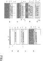
Figs. 1(a) to 1(h) are cross-sectional views illustrating the process of a method for manufacturing a glass device according to a first embodiment of the present invention. -
Figs. 2(a) to 2(h) are cross-sectional views illustrating the process of a method for manufacturing a glass device according to a second embodiment of the present invention. -
Fig. 3 illustrates the relationship between a laser modified area M1 and a thickness T1 of a glass substrate yet to be thinned (before being reduced in thickness). -
Fig. 4 illustrates the relationship between a diameter D1 of through holes and a thickness T2 of a glass substrate treated using hydrofluoric acid. -
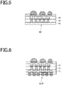
Fig. 5 illustrates an example of an RF-enabled glass device according to the present invention. -
Fig. 6 illustrates a glass interposer as an example of a glass device according to the present invention. - Embodiments of the present invention will now be described with reference to the drawings.
- It should be noted that the description below relates to examples of the present invention, and the invention is not limited by these examples.
- A method for manufacturing a glass device according to a first embodiment will now be described with reference to
Fig. 1 . - First, as illustrated in
Fig. 1(a) , aglass substrate 10 is irradiated with laser light on afirst surface 10a to form a laser modifiedarea 20 which is a starting point of athrough hole 40. The laser modifiedarea 20 is formed in a manner to extend downward from thefirst surface 10a, for example, in a vertical direction, with its lower end within theglass substrate 10. - Then, as illustrated in
Fig. 1(b) , a hydrofluoric acidresistant metal film 11 is formed on thefirst surface 10a of theglass substrate 10 within the range of 10 nm to 500 nm. Then, the hydrofluoric acidresistant metal film 11 is covered with acopper layer 111 within the range of 100 nm to 500 nm. In step 2, aseed layer 112 is formed on thefirst surface 10a of theglass substrate 10. The material for the hydrofluoric acidresistant metal film 11 may be selected as appropriate from, for example, chromium, nickel, and nickel-chromium. - Then, as illustrated in
Fig. 1(c) , a photoresist is formed with an intended pattern. Typically, a dry photoresist is used. In this step, however, thefirst surface 10a is laminated with a photosensitive film such as RD-1225 manufactured by Hitachi Chemical Company, Ltd, for direct imaging. Next, the determined pattern is imaged and then developed to expose theseed layer 112 formed in step 2. The exposed seed layer is fed with power to provide electrolytic copper plating having a thickness of 2 µm or more and 10 µm or less. The dry film resist no longer needed after the plating is dissolved away, and etching for a seed layer is performed to provide wiring. - Then, as illustrated in
Fig. 1(d) , thefirst surface 10a is laminated with an insulatingresin 12, and blind vias are formed in the insulatingresin 12 using a laser. Next, the insulatingresin 12 is laminated with a dry film resist, and a predetermined pattern is imaged and then developed. Then, the dry film resist no longer needed is dissolved away, and the wiring is provided. After the wiring is produced, a solder resistlayer 13 is formed. Thus, a first-surface wiring layer 14 which is a wiring on thefirst surface 10a is formed. - Then, as illustrated in
Fig. 1(e) , aglass carrier 30 corresponding to a support body is bonded to the first-surface wiring layer 14 via an adhesive 35 for temporary bonding. Theglass carrier 30 desirably has a thickness within the range of 0.7 mm to 1.5 mm in view of the conveyance after being thinned. The thickness of theglass carrier 30 may be determined as appropriate in accordance with the thickness of the glass substrate. Although theglass carrier 30 is illustrated as the support body, the support body may not be glass, but may be metal or resin. - Then, as illustrated in
Fig. 1(f) , on the circuit board formed by bonding theglass carrier 30 and theglass substrate 10 to each other using the adhesive 35, the surface of theglass substrate 10 opposite to thefirst surface 10a (or the lower surface in the figure) is etched with a hydrogen fluoride solution. The glass area outside the laser modifiedarea 20 is etched by the hydrogen fluoride solution and thinned in parallel with thefirst surface 10a of theglass substrate 10. When the hydrogen fluoride solution comes into contact with the laser modifiedarea 20, the laser modifiedarea 20 is dissolved preferentially, and thus the throughhole 40 is formed. In this manner, while theglass substrate 10 is being thinned, the throughhole 40 is formed. That is, thinning and the formation of the throughhole 40 are performed in a single etching. The bottom surface of the thinnedglass substrate 10 is asecond surface 10b on which a second-surface wiring layer 15 is formed. - An etching amount of the hydrogen fluoride solution may be determined as appropriate in accordance with the thickness of the glass device. For example, if the
glass substrate 10 used in step 1 has a thickness T1 of 400 µm, the etching amount may be desirably 100 µm or more and 350 µm or less. - The thinned
glass substrate 10 preferably has a thickness T2 of 50 µm or more and 300 µm or less. - Then, as illustrated in
Fig. 1(g) , steps 1 and 2 are performed as step 7. More specifically, a seed layer for power feeding is formed on the second surface having the throughhole 40 formed in it, and a dry film resist is patterned. Next, the seed layer is fed with power to provide electroplating having a thickness of 2 µm or more and 10 µm or less, and then the dry film resist no longer needed is dissolved away. Thus, a through electrode is formed. Then, the seed layer no longer needed is removed, and the surface is coated with an outer layer protective film such as an insulating resin or a solder resist. - The seed layer for power feeding on the second surface may be made from a material different from hydrofluoric acid resistant metals because of the absence of etching using hydrofluoric acid in the subsequent step. In this case, the side surface of the through
hole 40 is provided with a metal layer made from a material different from hydrofluoric acid resistant metals. Examples of materials different from hydrofluoric acid resistant metals include Ti, Cu, and electroless Ni, and at least one metal layer made from such a material is formed at least on the side surface of the throughhole 40. The material and the number of layers may be determined in any other appropriate manner. - The first wiring and the second wiring each include one or more layers. The number of layers may be determined as appropriate.
- If any external connection terminal is needed, an opening may be formed. The coating using an outer layer protective film such as an insulating resin or a solder resist forms the second-
surface wiring layer 15 which is wiring on thesecond surface 10b side. - Then, as illustrated in
Fig. 1(h) , theglass carrier 30 temporary bonded at step 5 is removed. Then, the glass device is completed. - A method for manufacturing a glass device according to a second embodiment will now be described with reference to
Fig. 2 . - First, as illustrated in
Fig. 2(a) , a hydrofluoric acidresistant metal film 11 is formed within the range of 10 nm to 500 nm on afirst surface 10a of aglass substrate 10, and acopper layer 111 is deposited within the range of 100 nm to 500 nm on the hydrofluoric acidresistant metal film 11 to form aseed layer 112. The material for the hydrofluoric acidresistant metal film 11 may be selected as appropriate from, for example, chromium, nickel, and nickel-chromium. - Then, as illustrated in
Fig. 2(b) , a photoresist is formed with a predetermined pattern on thefirst surface 10a of theglass substrate 10. Typically, a dry film resist is used. In this step, however, thefirst surface 10a of theglass substrate 10 is laminated with a photosensitive film such as RD-1225 for direct imaging, manufactured by Hitachi Chemical Company, Ltd. Next, the predetermined pattern is imaged and then developed to expose theseed layer 112 formed at step 1. The exposed seed layer is fed with power to provide electrolytic copper plating with a thickness of 2 µm or more and 10 µm or less. After the plating, the dry film resist no longer needed is dissolved away, and the seed layer is removed to provide wiring. - Then, as illustrated in
Fig. 2(c) , thefirst surface 10a is laminated using an insulatingresin 12, and blind vias are formed in the insulatingresin 12 using a laser. Next, the insulatingresin 12 is laminated with a dry film resist, and a predetermined pattern is imaged and then developed. Then, the dry film resist no longer needed is dissolved away, and the wiring is provided. After the wiring is produced, a solder resistlayer 13 is formed. Thus, a first-surface wiring layer 14 which is a wiring on thefirst surface 10a is formed. - Then, as illustrated in
Fig. 2(d) , aglass carrier 30 is bonded to the first-surface wiring layer 14 using an adhesive 35 for temporary bonding. Theglass carrier 30 desirably has a thickness within the range of 0.7 mm to 1.5 mm in view of the conveyance after being thinned. The thickness of theglass carrier 30 may be determined as appropriate in accordance with the thickness of theglass substrate 10. - Then, as illustrated in
Fig. 2(e) , the surface opposite to thefirst surface 10a of the glass substrate 10 (or the lower surface in the figure) is irradiated with laser light to form a laser modifiedarea 20 in theglass substrate 10. The laser modifiedarea 20 is formed to be perpendicular to the hydrofluoric acidresistant metal film 11 formed at step 1, with its lower end within theglass substrate 10. - Then, as illustrated in
Fig. 2(f) , on the glass substrate in which the laser modifiedarea 20 is formed at step 5, the surface opposite to thefirst surface 10a (or the lower surface in the figure) is etched with a hydrogen fluoride solution. The glass area without the laser modifiedarea 20 is etched by the hydrogen fluoride solution, and theglass substrate 10 is thinned in parallel with the first-surface wiring layer 14. When the hydrogen fluoride solution comes into contact with the laser modifiedarea 20, the laser modifiedarea 20 is dissolved preferentially, and thus the throughhole 40 is formed. In this manner, while theglass substrate 10 is being thinned, the throughhole 40 is formed. The bottom surface of the thinnedglass substrate 10 is asecond surface 10b on which a second-surface wiring layer 15 is formed. - The etching amount of the hydrogen fluoride solution may be determined as appropriate in accordance with the thickness of the glass device. For example, if the glass substrate used at step 1 has a thickness T1 of 400 µm, the etching amount may desirably be 100 µm or more and 350 µm or less.
- The thinned
glass substrate 10 preferably has a thickness T2 of 50 µm or more and 300 µm or less. - Then, as illustrated in
Fig. 2(g) , an electroless nickel plating layer or an electroless copper plating layer is formed as a seed layer for power feeding on thesecond surface 10b in which the throughhole 40 formed therein, and a dry film resist is patterned. The seed layer is fed with power to provide electroplating having a thickness of 2 µm or more and 10 µm or less. Next, the dry film resist no longer needed is dissolved away to form a through electrode. Then, the seed layer no longer needed is removed, and the surface is coated with an outer layer protective film such as an insulating resin or a solder resist layer. If any external connection terminal is required, an opening may be formed. The coating using an outer layer protective film such as an insulating resin or a solder resist forms the second wiring layer which is wiring on thesecond surface 10b side. - The first-
surface wiring layer 14 and the second-surface wiring layer 15 are each electrically connected to the through electrode formed in the throughhole 40 via the hydrofluoric acidresistant metal film 11. - Then, as illustrated in
Fig. 2(h) , theglass carrier 30 temporary bonded at step 5 is removed. Thus, the glass device is completed. - The laser modified
area 20 is a linear or rod-like area extending downward from thefirst surface 10a of theglass substrate 10, for example, in a direction perpendicular to thefirst surface 10a. The laser modifiedarea 20 has a length determined to be smaller than the thickness T1 of theglass substrate 10 at step 1 which is yet to be thinned. More specifically, the length of the laser modifiedarea 20 depends on the thickness of theglass substrate 10 in the final glass device. - The laser modified
areas 20 illustrated inFigs. 1(a) and2(e) are formed in the glass using laser light having a wavelength λ of 535 nm or less. The wavelength λ preferably falls within the range of 355 nm to 535 nm. Wavelengths λ lower than 355 nm cannot easily attain laser output, making it difficult to form the laser modifiedarea 20 in a stable manner. In contrast, wavelengths λ higher than 535 nm will enlarge the irradiation spot, making it difficult to form the laser modifiedarea 20. In addition, ablation may be used instead of modification due to thermal influence. However, microcracks may easily occur and therefore the laser modifiedarea 20 may easily be damaged. - The laser pulse width desirably ranges from picoseconds to femtoseconds. If the laser pulse width is nanoseconds or longer, it may be difficult to control the amount of energy per pulse, and microcracks may easily occur. Therefore, the laser modified
area 20 may easily be damaged. - The laser pulse energy has a preferable value selected depending on the material for the
glass substrate 10 and the details of the laser modifiedarea 20. In an example, the laser pulse energy falls within the range of 5 µJ to 150 µJ. If the laser pulse energy is increased, the laser modifiedarea 20 may become proportionally longer. - The etchant that is produced of the hydrogen fluoride solution illustrated in
Figs. 1(f) and2(f) includes one or more inorganic acids selected from the group consisting of nitric acid, hydrochloric acid, and sulfuric acid, as the hydrogen fluoride solution. - The hydrofluoric acid concentration is desirably, for example, 1.0 wt % or more and 6.0 wt % or less, and preferably 2.0 wt % or more and 5.0 wt % or less.
- The inorganic acid concentration falls within the range of 1.0 wt % to 20.0 wt % and preferably 3.0 wt % to 16.0 wt %. Using the hydrogen fluoride solution set within the above ranges, and setting the etching rate at 1.0 µm/min or less can perform etching in a desirable manner. During the etching, the etchant desirably has a temperature of 10°C or more and 40°C or less.
- Etching using the hydrogen fluoride solution is performed uniformly over the entire surface opposite to the
first surface 10a. In this process, the etching is performed in parallel with thefirst surface 10a toward thefirst surface 10a until the etchant reaches the laser modifiedarea 20. Then, the glass is thinned. When the hydrogen fluoride solution reaches an end of the laser modifiedarea 20, the laser modifiedarea 20 is preferentially etched, and the throughhole 40 is formed along the laser modifiedarea 20. - The etching is performed toward the
first surface 10a from the bottom, so that the formed throughhole 40 has the shape of a truncated cone tapered toward thefirst surface 10a from thesecond surface 10b, that is, the second surface side opening has the larger diameter (bottom). The throughhole 40 is processed so that the diameter of the first surface side opening and the diameter of the second surface side opening (bottom opening diameter) satisfy the relationship of, for example, (second surface side opening diameter/first surface side opening diameter) being 1.8 or more and 2.2 or less. - As shown in
Figs. 3 and 4 , the laser modifiedarea 20 has a length M1 that can be calculated from the glass thickness T2 after the etching using the hydrogen fluoride solution and the second-surface diameter D1 of the through hole, and more specifically, M1 = (D1/2) + T2 or substantially M1 = (D1/2) + T2. The expression "substantially M1 = (D1/2) + T2" means that M1 is substantially equal to (D1/2) + T2, and for example, |M1|/|(D1/2) + T2)| is 0.95 or more and 1.05 or less. Thus, the length M1 of the laser modifiedarea 20 may be determined as appropriate based on the diameter D1 of the desired through hole and the glass thickness T2 of after the etching. The etching amount of the hydrogen fluoride solution can be calculated from T1 - T2, which is the reduced thickness. - The method for manufacturing a glass device according to the present embodiment enables a glass device having a glass substrate with a glass thickness of 300 µm or less to be manufactured more easily by providing wiring on the
first surface 10a and then forming a through hole while thinning the glass substrate by etching. - In manufacturing, the through hole is formed while the glass is being thinned by etching in a state in which the
glass substrate 10 is supported on theglass carrier 30. This ensures the ease of handling the glass substrate when conductive portions such as circuits are formed, and allows stable production of a glass device having through electrodes that has a glass substrate of 300 µm or less in thickness. - The etching for thinning the glass and forming the through hole may be performed not in a single process but in multiple processes. In other words, the glass thinning and the through hole formation may be achieved by one or more etching steps.
- The glass device described above may be used as a glass device such as an RF device illustrated in
Fig. 5 or a glass interposer illustrated inFig. 6 . The present embodiment may also be used for a glass device having through electrodes, because the present embodiment easily adjusts the thickness of the glass device and forms the through electrodes in through holes. - The scope of the present invention is not limited to the illustrated and described exemplary embodiments, but includes all embodiments that provide effects equivalent to the intended effects of the present invention. Furthermore, the scope of the present invention is not limited to combinations of features recited in the claims, but may be defined by any desired combination of specific features among all the disclosed features.
- This application claims the benefit of priority from Japanese Patent Application No.
2018-110668 (filed on June 8, 2018 -
- 10: Glass substrate
- 11: Hydrofluoric acid resistant metal film
- 12: Insulating resin
- 13: Solder resist layer
- 14: Wiring layer on first surface (first wiring)
- 15: Wiring layer on second surface (second wiring)
- 20: Laser modified area
- 30: Glass carrier (support body)
- 35: Adhesive
- 40: Through hole
- T1: Thickness of glass substrate
- T2: Thickness of etched glass substrate
- M1: Length of laser modified area
- D1: Second surface side diameter of through hole
- RF: RF device
- G-IP: Glass interposer
Claims (10)
- A method for manufacturing a glass device having one or more through holes formed in a glass substrate, and a first wiring on a first surface of the glass substrate and a second wiring on a second surface opposite to the first surface being electrically connected to each other via the through holes, comprising:providing the first wiring;forming the through holes while thinning the glass substrate by etching;providing wiring into the through holes and the second wiring; andconnecting the first wiring and the second wiring to each other via the wiring into the through holes, characterized in thatthe glass substrate has the through holes formed with a thickness of 50 µm or more and 300 µm or less, andthe through holes have a shape of a truncated cone and having a second surface side opening being a bottom surface, and a ratio of (second surface side opening diameter/first surface side opening diameter) which is a relationship between a diameter of a first surface side opening and a diameter of the second surface side opening is 1.8 or more and 2.2 or less.
- A method for manufacturing a glass device, comprising the steps of:providing a first wiring on a first surface of a glass substrate;supporting a first wiring side of the glass substrate provided with the first wiring, using a support body;forming a laser modified area using a laser light applied to a surface opposite to the first surface, the laser modified area extending from the first surface of the glass substrate toward a surface opposite to the first surface and serving as an area from which a through hole is formed;forming a through hole while thinning the glass substrate by etching using a hydrogen fluoride etchant toward the first surface from the surface opposite to the first surface of the glass substrate, after the step of supporting the first wiring side of the glass substrate and the step of forming the laser modified area;forming a through electrode inside the through hole, and providing a second wiring on a surface opposite to the first surface of the glass substrate, and connecting the first wiring and the second wiring to each other via the through electrode after the step of forming the through hole; andremoving the support body from the glass substrate after the second wiring is formed.
- The method for manufacturing a glass device according to claim 2, characterized in that
the laser modified area is formed before the first wiring is formed or after the first wiring is provided to the glass substrate. - The method for manufacturing a glass device according to claim 2 or 3, characterized in that
the glass substrate after the step of forming the through hole has a thickness of 50 µm or more and 300 µm or less. - The method for manufacturing a glass device according to any one of claims 2 to 4, characterized in that
the laser light used to form the laser modified area has a laser pulse width in the range of picoseconds to femtoseconds. - The method for manufacturing a glass device according to any one of claims 2 to 5, characterized in that
the through hole has a truncated cone shape having a large diameter in the surface opposite to the first surface, and
a relationship of M1 = (D1/2) + T2 or substantially M1 = (D1/2) + T2 is satisfied wherein
the large diameter of the through hole in the surface opposite to the first surface is denoted by D1, the glass substrate after the etching using hydrogen fluoride has a thickness denoted by T2, and the laser modified area has a length denoted by M1. - The method for manufacturing a glass device according to any one of claims 2 to 6, characterized in that
the through electrode is formed by plating after a seed layer to which a conductive material included in the through electrode is attached is formed on an inner periphery of the through hole. - The method for manufacturing a glass device according to any one of claims 2 to 7, characterized in that
the first wiring and the second wiring each comprise one or more layers. - A glass device provided with one or more through holes formed in a glass substrate, a first wiring on a first surface of the glass substrate and a second wiring on a second surface opposite to the first surface being electrically connected to each other via a through electrode formed in the through holes, characterized in that
the through electrodes are electrically connected to the first wiring and the second wiring through a hydrofluoric acid resistant metal material including one or more layers selected from chromium, nickel, and nickel-chromium alloy,
the glass substrate has a thickness of 50 µm or more and 300 µm or less, and
the through holes have a shape of a truncated cone and having a second surface side opening being a bottom surface, wherein a ratio of (second surface side opening diameter/first surface side opening diameter) which is a relationship between a diameter of a first surface side opening and a diameter of the second surface side opening is 1.8 or more and 2.2 or less. - The glass device according to claim 9, characterized in that
the through holes in the glass device each have a side surface provided with one or more metal layers formed of a metal different from the hydrofluoric acid resistant metal material.
Applications Claiming Priority (2)
| Application Number | Priority Date | Filing Date | Title |
|---|---|---|---|
| JP2018110668 | 2018-06-08 | ||
| PCT/JP2019/022745 WO2019235617A1 (en) | 2018-06-08 | 2019-06-07 | Method of manufacturing glass device and glass device |
Publications (2)
| Publication Number | Publication Date |
|---|---|
| EP3806141A1 true EP3806141A1 (en) | 2021-04-14 |
| EP3806141A4 EP3806141A4 (en) | 2021-08-04 |
Family
ID=68770332
Family Applications (1)
| Application Number | Title | Priority Date | Filing Date |
|---|---|---|---|
| EP19815365.2A Pending EP3806141A4 (en) | 2018-06-08 | 2019-06-07 | GLASS DEVICE AND GLASS DEVICE MANUFACTURING PROCESS |
Country Status (5)
| Country | Link |
|---|---|
| US (1) | US11881414B2 (en) |
| EP (1) | EP3806141A4 (en) |
| JP (2) | JP7298603B2 (en) |
| CN (1) | CN112335037B (en) |
| WO (1) | WO2019235617A1 (en) |
Families Citing this family (25)
| Publication number | Priority date | Publication date | Assignee | Title |
|---|---|---|---|---|
| US20200027728A1 (en) * | 2018-07-23 | 2020-01-23 | Intel Corporation | Substrate package with glass dielectric |
| JP7608727B2 (en) * | 2020-04-07 | 2025-01-07 | Toppanホールディングス株式会社 | Manufacturing method for glass core wiring board with built-in high frequency filter |
| CN112312654B (en) * | 2020-08-14 | 2021-09-17 | 珠海越亚半导体股份有限公司 | Passive device structure embedded in glass medium and manufacturing method thereof |
| JP2022151790A (en) * | 2021-03-26 | 2022-10-07 | 凸版印刷株式会社 | Method for manufacturing wiring board and wiring board |
| JP7700481B2 (en) * | 2021-03-26 | 2025-07-01 | Toppanホールディングス株式会社 | Method for manufacturing wiring board |
| JP2022151789A (en) * | 2021-03-26 | 2022-10-07 | 凸版印刷株式会社 | Method for manufacturing wiring board and wiring board |
| WO2022203037A1 (en) | 2021-03-26 | 2022-09-29 | 凸版印刷株式会社 | Wiring board manufacturing method and wiring board |
| US12322669B2 (en) * | 2021-04-23 | 2025-06-03 | Beijing Boe Sensor Technology Co., Ltd. | Substrate integrated with passive devices and manufacturing method thereof |
| US20220392832A1 (en) * | 2021-06-06 | 2022-12-08 | Taiwan Semiconductor Manufacturing Company, Ltd. | Semiconductor structures and methods of forming the same |
| JP7786091B2 (en) * | 2021-09-15 | 2025-12-16 | Toppanホールディングス株式会社 | wiring board |
| JP7067666B1 (en) * | 2021-11-30 | 2022-05-16 | 凸版印刷株式会社 | Manufacturing method of multi-layer wiring board |
| JP2023098209A (en) * | 2021-12-28 | 2023-07-10 | 凸版印刷株式会社 | Multilayer wiring board and manufacturing method thereof |
| CN114477779B (en) * | 2021-12-30 | 2023-09-08 | 厦门云天半导体科技有限公司 | Multi-layer glass substrate process and structure based on heterogeneous bonding |
| JP2023132151A (en) * | 2022-03-10 | 2023-09-22 | 凸版印刷株式会社 | Glass substrate, through electrode, multilayer wiring board, and glass substrate manufacturing method |
| CN117642980A (en) | 2022-06-24 | 2024-03-01 | 京东方科技集团股份有限公司 | Filter and preparation method thereof |
| CN115727981A (en) * | 2022-08-24 | 2023-03-03 | 西安交通大学 | Leadless packaged pressure chip flexible tactile measurement sensor and preparation method thereof |
| JP2024046350A (en) * | 2022-09-22 | 2024-04-03 | Toppanホールディングス株式会社 | Wiring Board |
| WO2024070319A1 (en) * | 2022-09-30 | 2024-04-04 | Toppanホールディングス株式会社 | Glass substrate, multilayer wiring substrate, and method for producing glass substrate |
| JP2024051691A (en) * | 2022-09-30 | 2024-04-11 | Toppanホールディングス株式会社 | Glass substrate, multilayer wiring substrate, and method for manufacturing glass substrate |
| CN119096704A (en) * | 2022-10-13 | 2024-12-06 | 株式会社力森诺科 | Method for manufacturing thin wiring component, method for manufacturing thin wiring component and wiring substrate |
| JP2024071115A (en) | 2022-11-14 | 2024-05-24 | Toppanホールディングス株式会社 | Wiring board and method for manufacturing the same |
| US12616026B2 (en) | 2022-11-30 | 2026-04-28 | Intel Corporation | Permanent layer for bump chip attach |
| CN116033659A (en) * | 2022-12-30 | 2023-04-28 | 珠海杰赛科技有限公司 | A processing method of zero overflow glue blind groove and blind groove plate made thereof |
| WO2025258471A1 (en) * | 2024-06-12 | 2025-12-18 | Toppanホールディングス株式会社 | Multilayer wiring board, semiconductor device, and method for manufacturing multilayer wiring board |
| CN119952307B (en) * | 2025-01-21 | 2026-02-17 | 湖北通格微电路科技有限公司 | Methods for thinning glass through holes |
Family Cites Families (22)
| Publication number | Priority date | Publication date | Assignee | Title |
|---|---|---|---|---|
| JPS54126215A (en) | 1978-03-24 | 1979-10-01 | Central Glass Co Ltd | Drilling plate glass |
| JP2000061667A (en) | 1998-08-19 | 2000-02-29 | Junichi Ikeno | Laser processing method of glass and glass molded product |
| JP2001105398A (en) | 1999-03-04 | 2001-04-17 | Seiko Epson Corp | Processing method |
| JP4092890B2 (en) * | 2001-05-31 | 2008-05-28 | 株式会社日立製作所 | Multi-chip module |
| JP2005190857A (en) | 2003-12-26 | 2005-07-14 | Seiko Epson Corp | MASK, MASK MANUFACTURING METHOD, ORGANIC ELECTROLUMINESCENT DEVICE MANUFACTURING METHOD, ORGANIC ELECTROLUMINESCENT DEVICE MANUFACTURING DEVICE, ORGANIC ELECTROLUMINESCENT DEVICE, AND ELECTRONIC DEVICE |
| JP2008203336A (en) | 2007-02-16 | 2008-09-04 | Fujikura Ltd | Photoelectric composite substrate, manufacturing method thereof, and electronic device |
| JP2011178642A (en) | 2010-03-03 | 2011-09-15 | Nippon Sheet Glass Co Ltd | Method for producing glass sheet with through-electrode, and electronic component |
| JP2013080904A (en) * | 2011-09-22 | 2013-05-02 | Hoya Corp | Substrate manufacturing method, wiring board manufacturing method, glass substrate, and wiring board |
| JP5922254B2 (en) * | 2012-11-21 | 2016-05-24 | アルバック成膜株式会社 | Manufacturing method of functional parts |
| CN105228788A (en) | 2012-11-29 | 2016-01-06 | 康宁股份有限公司 | For sacrifice cover layer and the method thereof of laser drill base material |
| US20140247269A1 (en) | 2013-03-04 | 2014-09-04 | Qualcomm Mems Technologies, Inc. | High density, low loss 3-d through-glass inductor with magnetic core |
| JP6201622B2 (en) * | 2013-10-21 | 2017-09-27 | 日立化成株式会社 | Connection terminal and semiconductor chip mounting board using the same |
| JP2015211162A (en) * | 2014-04-28 | 2015-11-24 | 旭硝子株式会社 | Method for manufacturing glass member, glass member, and glass interposer |
| JP2016072433A (en) | 2014-09-30 | 2016-05-09 | 大日本印刷株式会社 | Through electrode substrate and manufacturing method thereof |
| KR102391793B1 (en) * | 2014-10-03 | 2022-04-28 | 니혼 이타가라스 가부시키가이샤 | Method for producing glass substrate with through-electrode, and glass substrate |
| JP6545699B2 (en) * | 2014-10-22 | 2019-07-17 | 日本板硝子株式会社 | Method of manufacturing glass substrate, glass substrate, and assembly |
| JP6657609B2 (en) * | 2015-06-12 | 2020-03-04 | 凸版印刷株式会社 | Wiring circuit board, semiconductor device, method of manufacturing wiring circuit board, and method of manufacturing semiconductor device |
| JP5994954B1 (en) * | 2015-09-25 | 2016-09-21 | 旭硝子株式会社 | Manufacturing method of glass substrate having through hole, manufacturing method of glass substrate having through electrode, and manufacturing method of interposer |
| JP6840935B2 (en) * | 2016-05-10 | 2021-03-10 | 凸版印刷株式会社 | Wiring circuit board manufacturing method |
| US9917046B2 (en) | 2016-07-04 | 2018-03-13 | Unimicron Technology Corp. | Manufacturing method of a circuit board having a glass film |
| JP2018110668A (en) | 2017-01-10 | 2018-07-19 | 株式会社三共 | Management device |
| US10814133B2 (en) * | 2017-02-06 | 2020-10-27 | Zyvex Labs, Llc | Methods of fabricating an implantable device |
-
2019
- 2019-06-07 EP EP19815365.2A patent/EP3806141A4/en active Pending
- 2019-06-07 JP JP2020523206A patent/JP7298603B2/en active Active
- 2019-06-07 CN CN201980036910.6A patent/CN112335037B/en active Active
- 2019-06-07 WO PCT/JP2019/022745 patent/WO2019235617A1/en not_active Ceased
-
2020
- 2020-12-07 US US17/113,929 patent/US11881414B2/en active Active
-
2023
- 2023-06-15 JP JP2023098424A patent/JP7647801B2/en active Active
Also Published As
| Publication number | Publication date |
|---|---|
| JP2023126229A (en) | 2023-09-07 |
| CN112335037A (en) | 2021-02-05 |
| EP3806141A4 (en) | 2021-08-04 |
| CN112335037B (en) | 2024-11-26 |
| WO2019235617A1 (en) | 2019-12-12 |
| JP7298603B2 (en) | 2023-06-27 |
| US20210118698A1 (en) | 2021-04-22 |
| US11881414B2 (en) | 2024-01-23 |
| JPWO2019235617A1 (en) | 2021-07-15 |
| JP7647801B2 (en) | 2025-03-18 |
Similar Documents
| Publication | Publication Date | Title |
|---|---|---|
| US11881414B2 (en) | Method for manufacturing glass device, and glass device | |
| CN100364092C (en) | Semiconductor device and production method thereof | |
| JP6840935B2 (en) | Wiring circuit board manufacturing method | |
| JP7569516B2 (en) | Structure | |
| US20160079149A1 (en) | Wiring board provided with through electrode, method for manufacturing same and semiconductor device | |
| JP2022133310A (en) | Penetration electrode substrate, manufacturing method thereof, and mounting substrate | |
| US9485864B2 (en) | Bump structure, wiring substrate, semiconductor apparatus and bump structure manufacturing method | |
| CN101809735A (en) | Interconnection element with posts formed by plating | |
| CN107567651B (en) | Wiring board with through-electrode and method of manufacturing the same | |
| US9924596B2 (en) | Structural body and method for manufacturing same | |
| WO2017202037A1 (en) | Conductor post and manufacturing method thereof, chip packaging method, and flip chip product | |
| JP2015156424A (en) | Printed circuit board, semiconductor device, and manufacturing method thereof | |
| US6822332B2 (en) | Fine line circuitization | |
| KR20110025250A (en) | Method for manufacturing copper bumps of fine pitch | |
| US12557211B2 (en) | Package having thick glass core with high aspect ratio vias | |
| CN105655321A (en) | Electronic packages and methods of making and using same | |
| KR101039774B1 (en) | Bump Formation Method for Printed Circuit Board Manufacturing | |
| TW202431908A (en) | Wiring board | |
| EP4319512A1 (en) | Wiring board manufacturing method and wiring board | |
| US9837342B2 (en) | Multilayer wiring board and method for manufacturing same | |
| JP2022151790A (en) | Method for manufacturing wiring board and wiring board | |
| CN121772757A (en) | Packaging carrier plate, preparation method thereof and chip packaging structure | |
| JP2000307242A (en) | Circuit board manufacturing method, circuit board, and semiconductor device |
Legal Events
| Date | Code | Title | Description |
|---|---|---|---|
| STAA | Information on the status of an ep patent application or granted ep patent |
Free format text: STATUS: THE INTERNATIONAL PUBLICATION HAS BEEN MADE |
|
| PUAI | Public reference made under article 153(3) epc to a published international application that has entered the european phase |
Free format text: ORIGINAL CODE: 0009012 |
|
| STAA | Information on the status of an ep patent application or granted ep patent |
Free format text: STATUS: REQUEST FOR EXAMINATION WAS MADE |
|
| 17P | Request for examination filed |
Effective date: 20201102 |
|
| AK | Designated contracting states |
Kind code of ref document: A1 Designated state(s): AL AT BE BG CH CY CZ DE DK EE ES FI FR GB GR HR HU IE IS IT LI LT LU LV MC MK MT NL NO PL PT RO RS SE SI SK SM TR |
|
| AX | Request for extension of the european patent |
Extension state: BA ME |
|
| A4 | Supplementary search report drawn up and despatched |
Effective date: 20210706 |
|
| RIC1 | Information provided on ipc code assigned before grant |
Ipc: H01L 23/15 20060101AFI20210630BHEP Ipc: B23K 26/53 20140101ALI20210630BHEP Ipc: C03C 15/00 20060101ALI20210630BHEP Ipc: H01L 23/32 20060101ALI20210630BHEP Ipc: H01L 21/48 20060101ALI20210630BHEP |
|
| DAV | Request for validation of the european patent (deleted) | ||
| DAX | Request for extension of the european patent (deleted) |