EP3787167A1 - Flying capacitor converter - Google Patents
Flying capacitor converter Download PDFInfo
- Publication number
- EP3787167A1 EP3787167A1 EP20174658.3A EP20174658A EP3787167A1 EP 3787167 A1 EP3787167 A1 EP 3787167A1 EP 20174658 A EP20174658 A EP 20174658A EP 3787167 A1 EP3787167 A1 EP 3787167A1
- Authority
- EP
- European Patent Office
- Prior art keywords
- capacitor
- diode
- node
- voltage
- coupled
- Prior art date
- Legal status (The legal status is an assumption and is not a legal conclusion. Google has not performed a legal analysis and makes no representation as to the accuracy of the status listed.)
- Granted
Links
Images




Classifications
-
- H—ELECTRICITY
- H02—GENERATION; CONVERSION OR DISTRIBUTION OF ELECTRIC POWER
- H02M—APPARATUS FOR CONVERSION BETWEEN AC AND AC, BETWEEN AC AND DC, OR BETWEEN DC AND DC, AND FOR USE WITH MAINS OR SIMILAR POWER SUPPLY SYSTEMS; CONVERSION OF DC OR AC INPUT POWER INTO SURGE OUTPUT POWER; CONTROL OR REGULATION THEREOF
- H02M3/00—Conversion of DC power input into DC power output
- H02M3/02—Conversion of DC power input into DC power output without intermediate conversion into AC
- H02M3/04—Conversion of DC power input into DC power output without intermediate conversion into AC by static converters
- H02M3/10—Conversion of DC power input into DC power output without intermediate conversion into AC by static converters using discharge tubes with control electrode or semiconductor devices with control electrode
- H02M3/145—Conversion of DC power input into DC power output without intermediate conversion into AC by static converters using discharge tubes with control electrode or semiconductor devices with control electrode using devices of a triode or transistor type requiring continuous application of a control signal
- H02M3/155—Conversion of DC power input into DC power output without intermediate conversion into AC by static converters using discharge tubes with control electrode or semiconductor devices with control electrode using devices of a triode or transistor type requiring continuous application of a control signal using semiconductor devices only
- H02M3/156—Conversion of DC power input into DC power output without intermediate conversion into AC by static converters using discharge tubes with control electrode or semiconductor devices with control electrode using devices of a triode or transistor type requiring continuous application of a control signal using semiconductor devices only with automatic control of output voltage or current, e.g. switching regulators
- H02M3/158—Conversion of DC power input into DC power output without intermediate conversion into AC by static converters using discharge tubes with control electrode or semiconductor devices with control electrode using devices of a triode or transistor type requiring continuous application of a control signal using semiconductor devices only with automatic control of output voltage or current, e.g. switching regulators including plural semiconductor devices as final control devices for a single load
-
- H—ELECTRICITY
- H02—GENERATION; CONVERSION OR DISTRIBUTION OF ELECTRIC POWER
- H02M—APPARATUS FOR CONVERSION BETWEEN AC AND AC, BETWEEN AC AND DC, OR BETWEEN DC AND DC, AND FOR USE WITH MAINS OR SIMILAR POWER SUPPLY SYSTEMS; CONVERSION OF DC OR AC INPUT POWER INTO SURGE OUTPUT POWER; CONTROL OR REGULATION THEREOF
- H02M3/00—Conversion of DC power input into DC power output
- H02M3/02—Conversion of DC power input into DC power output without intermediate conversion into AC
- H02M3/04—Conversion of DC power input into DC power output without intermediate conversion into AC by static converters
- H02M3/10—Conversion of DC power input into DC power output without intermediate conversion into AC by static converters using discharge tubes with control electrode or semiconductor devices with control electrode
- H02M3/145—Conversion of DC power input into DC power output without intermediate conversion into AC by static converters using discharge tubes with control electrode or semiconductor devices with control electrode using devices of a triode or transistor type requiring continuous application of a control signal
- H02M3/155—Conversion of DC power input into DC power output without intermediate conversion into AC by static converters using discharge tubes with control electrode or semiconductor devices with control electrode using devices of a triode or transistor type requiring continuous application of a control signal using semiconductor devices only
- H02M3/156—Conversion of DC power input into DC power output without intermediate conversion into AC by static converters using discharge tubes with control electrode or semiconductor devices with control electrode using devices of a triode or transistor type requiring continuous application of a control signal using semiconductor devices only with automatic control of output voltage or current, e.g. switching regulators
- H02M3/158—Conversion of DC power input into DC power output without intermediate conversion into AC by static converters using discharge tubes with control electrode or semiconductor devices with control electrode using devices of a triode or transistor type requiring continuous application of a control signal using semiconductor devices only with automatic control of output voltage or current, e.g. switching regulators including plural semiconductor devices as final control devices for a single load
- H02M3/1584—Conversion of DC power input into DC power output without intermediate conversion into AC by static converters using discharge tubes with control electrode or semiconductor devices with control electrode using devices of a triode or transistor type requiring continuous application of a control signal using semiconductor devices only with automatic control of output voltage or current, e.g. switching regulators including plural semiconductor devices as final control devices for a single load with a plurality of power processing stages connected in parallel
-
- H—ELECTRICITY
- H02—GENERATION; CONVERSION OR DISTRIBUTION OF ELECTRIC POWER
- H02H—EMERGENCY PROTECTIVE CIRCUIT ARRANGEMENTS
- H02H9/00—Emergency protective circuit arrangements for limiting excess current or voltage without disconnection
- H02H9/04—Emergency protective circuit arrangements for limiting excess current or voltage without disconnection responsive to excess voltage
-
- H—ELECTRICITY
- H02—GENERATION; CONVERSION OR DISTRIBUTION OF ELECTRIC POWER
- H02M—APPARATUS FOR CONVERSION BETWEEN AC AND AC, BETWEEN AC AND DC, OR BETWEEN DC AND DC, AND FOR USE WITH MAINS OR SIMILAR POWER SUPPLY SYSTEMS; CONVERSION OF DC OR AC INPUT POWER INTO SURGE OUTPUT POWER; CONTROL OR REGULATION THEREOF
- H02M1/00—Details of apparatus for conversion
- H02M1/08—Circuits specially adapted for the generation of control voltages for semiconductor devices incorporated in static converters
-
- H—ELECTRICITY
- H02—GENERATION; CONVERSION OR DISTRIBUTION OF ELECTRIC POWER
- H02M—APPARATUS FOR CONVERSION BETWEEN AC AND AC, BETWEEN AC AND DC, OR BETWEEN DC AND DC, AND FOR USE WITH MAINS OR SIMILAR POWER SUPPLY SYSTEMS; CONVERSION OF DC OR AC INPUT POWER INTO SURGE OUTPUT POWER; CONTROL OR REGULATION THEREOF
- H02M1/00—Details of apparatus for conversion
- H02M1/32—Means for protecting converters other than automatic disconnection
-
- H—ELECTRICITY
- H02—GENERATION; CONVERSION OR DISTRIBUTION OF ELECTRIC POWER
- H02M—APPARATUS FOR CONVERSION BETWEEN AC AND AC, BETWEEN AC AND DC, OR BETWEEN DC AND DC, AND FOR USE WITH MAINS OR SIMILAR POWER SUPPLY SYSTEMS; CONVERSION OF DC OR AC INPUT POWER INTO SURGE OUTPUT POWER; CONTROL OR REGULATION THEREOF
- H02M1/00—Details of apparatus for conversion
- H02M1/36—Means for starting or stopping converters
-
- H—ELECTRICITY
- H02—GENERATION; CONVERSION OR DISTRIBUTION OF ELECTRIC POWER
- H02M—APPARATUS FOR CONVERSION BETWEEN AC AND AC, BETWEEN AC AND DC, OR BETWEEN DC AND DC, AND FOR USE WITH MAINS OR SIMILAR POWER SUPPLY SYSTEMS; CONVERSION OF DC OR AC INPUT POWER INTO SURGE OUTPUT POWER; CONTROL OR REGULATION THEREOF
- H02M3/00—Conversion of DC power input into DC power output
- H02M3/02—Conversion of DC power input into DC power output without intermediate conversion into AC
- H02M3/04—Conversion of DC power input into DC power output without intermediate conversion into AC by static converters
- H02M3/06—Conversion of DC power input into DC power output without intermediate conversion into AC by static converters using resistors or capacitors, e.g. potential divider
- H02M3/07—Conversion of DC power input into DC power output without intermediate conversion into AC by static converters using resistors or capacitors, e.g. potential divider using capacitors charged and discharged alternately by semiconductor devices with control electrode, e.g. charge pumps
-
- H—ELECTRICITY
- H02—GENERATION; CONVERSION OR DISTRIBUTION OF ELECTRIC POWER
- H02M—APPARATUS FOR CONVERSION BETWEEN AC AND AC, BETWEEN AC AND DC, OR BETWEEN DC AND DC, AND FOR USE WITH MAINS OR SIMILAR POWER SUPPLY SYSTEMS; CONVERSION OF DC OR AC INPUT POWER INTO SURGE OUTPUT POWER; CONTROL OR REGULATION THEREOF
- H02M7/00—Conversion of AC power input into DC power output; Conversion of DC power input into AC power output
- H02M7/42—Conversion of DC power input into AC power output without possibility of reversal
- H02M7/44—Conversion of DC power input into AC power output without possibility of reversal by static converters
- H02M7/48—Conversion of DC power input into AC power output without possibility of reversal by static converters using discharge tubes with control electrode or semiconductor devices with control electrode
- H02M7/483—Converters with outputs that each can have more than two voltages levels
- H02M7/4837—Flying capacitor converters
-
- H—ELECTRICITY
- H10—SEMICONDUCTOR DEVICES; ELECTRIC SOLID-STATE DEVICES NOT OTHERWISE PROVIDED FOR
- H10D—INORGANIC ELECTRIC SEMICONDUCTOR DEVICES
- H10D8/00—Diodes
- H10D8/20—Breakdown diodes, e.g. avalanche diodes
- H10D8/25—Zener diodes
-
- H—ELECTRICITY
- H02—GENERATION; CONVERSION OR DISTRIBUTION OF ELECTRIC POWER
- H02M—APPARATUS FOR CONVERSION BETWEEN AC AND AC, BETWEEN AC AND DC, OR BETWEEN DC AND DC, AND FOR USE WITH MAINS OR SIMILAR POWER SUPPLY SYSTEMS; CONVERSION OF DC OR AC INPUT POWER INTO SURGE OUTPUT POWER; CONTROL OR REGULATION THEREOF
- H02M1/00—Details of apparatus for conversion
- H02M1/0003—Details of control, feedback or regulation circuits
-
- H—ELECTRICITY
- H02—GENERATION; CONVERSION OR DISTRIBUTION OF ELECTRIC POWER
- H02M—APPARATUS FOR CONVERSION BETWEEN AC AND AC, BETWEEN AC AND DC, OR BETWEEN DC AND DC, AND FOR USE WITH MAINS OR SIMILAR POWER SUPPLY SYSTEMS; CONVERSION OF DC OR AC INPUT POWER INTO SURGE OUTPUT POWER; CONTROL OR REGULATION THEREOF
- H02M1/00—Details of apparatus for conversion
- H02M1/0095—Hybrid converter topologies, e.g. NPC mixed with flying capacitor, thyristor converter mixed with MMC or charge pump mixed with buck
-
- H—ELECTRICITY
- H02—GENERATION; CONVERSION OR DISTRIBUTION OF ELECTRIC POWER
- H02M—APPARATUS FOR CONVERSION BETWEEN AC AND AC, BETWEEN AC AND DC, OR BETWEEN DC AND DC, AND FOR USE WITH MAINS OR SIMILAR POWER SUPPLY SYSTEMS; CONVERSION OF DC OR AC INPUT POWER INTO SURGE OUTPUT POWER; CONTROL OR REGULATION THEREOF
- H02M1/00—Details of apparatus for conversion
- H02M1/32—Means for protecting converters other than automatic disconnection
- H02M1/325—Means for protecting converters other than automatic disconnection with means for allowing continuous operation despite a fault, i.e. fault tolerant converters
-
- H—ELECTRICITY
- H02—GENERATION; CONVERSION OR DISTRIBUTION OF ELECTRIC POWER
- H02M—APPARATUS FOR CONVERSION BETWEEN AC AND AC, BETWEEN AC AND DC, OR BETWEEN DC AND DC, AND FOR USE WITH MAINS OR SIMILAR POWER SUPPLY SYSTEMS; CONVERSION OF DC OR AC INPUT POWER INTO SURGE OUTPUT POWER; CONTROL OR REGULATION THEREOF
- H02M1/00—Details of apparatus for conversion
- H02M1/32—Means for protecting converters other than automatic disconnection
- H02M1/34—Snubber circuits
- H02M1/346—Passive non-dissipative snubbers
Definitions
- the present disclosure relates to a flying capacitor converter, and more particularly to charging and circuit protection mechanisms for a flying capacitor converter.
- FIG. 1 shows a circuit diagram of a conventional flying capacitor converter (FCC).
- the FCC is essentially a DC-to-DC boost converter for stepping up a DC input voltage to a DC output voltage.
- the FCC includes an inductor L, a first switch S1, a second switch S2, a first diode D1, a second diode D2, a flying capacitor C F1 , and an output capacitor C.
- the first switch S1 is coupled in series to the second switch S2, and commonly connected at a node P S .
- the first diode D1 is coupled in series to the second diode D2, and commonly connected at a node P D .
- the flying capacitor C F1 is coupled between the node P S and the node P D .
- the DC output voltage is controlled by turning on and turning off the first switch S1 and the second switch S2.
- a first end of the inductor L is coupled to a positive end of a DC input voltage Vdc, and a second end of the inductor L is coupled to an anode of the first diode D1.
- the first switch S1 is coupled in series to the second switch S2, and a second end of the first switch S1 and a first end of the second switch S2 are commonly coupled to the node P S .
- a first end of the first switch S1, the second end of the inductor L, and the anode of the first diode D1 are commonly coupled to a node P L .
- a second end of the second switch S2 is coupled to a negative end of the DC input voltage Vdc.
- the first diode D1 is coupled in series to the second diode D2, and a cathode of the first diode D1 and an anode of the second diode D2 are commonly coupled to a node P D .
- the flying capacitor C F1 is coupled between the node P D and the node P S .
- a first end of the output capacitor C is coupled to a cathode of the second diode D2, and a second end of the output capacitor C is coupled to the negative end of the DC input voltage Vdc.
- An output that is the output capacitor C of the FCC is coupled to a load.
- the output capacitor C is for illustration only, and may actually consist of multiple capacitors connected in series and/or in parallel.
- the conventional flying capacitor converter has following disadvantages or problems: (1) the problem of the withstand voltage of the second switch S2, and (2) the problem of the withstand voltage of the second diode D2.
- An object of the present disclosure is to provide a flying capacitor converter to solve the problems of the related art.
- the flying capacitor converter receives a DC input voltage and converts the DC input voltage into a DC output voltage.
- the flying capacitor converter includes an inductor, a first switch and a second switch, a first diode and a second diode, a first capacitor and a second capacitor, a flying capacitor, a third diode and a third capacitor, a fourth diode, and a fifth diode.
- the inductor is coupled between a positive end of the DC input voltage and a first node.
- the first switch and the second switch are commonly coupled to a second node, and the first switch is coupled to the first node and the second switch is coupled to a negative end of the DC input voltage.
- the first diode and the second diode are commonly coupled to a third node, and the first diode is coupled to the first node.
- the first capacitor and the second capacitor are commonly coupled to a fourth node, and the first capacitor is coupled to the second diode and the second capacitor is coupled to the second switch and the negative end of the DC input voltage.
- the first capacitor and the second capacitor provide the DC output voltage, and the fourth node is a midpoint of the DC output voltage.
- the flying capacitor is coupled to the second node and the third node.
- the third diode and the third capacitor are commonly coupled to a fifth node, and the third diode is coupled to the second node and the third capacitor is coupled to the second switch and the negative end of the DC input voltage.
- the fourth diode is coupled to the second diode and the fifth node.
- the fifth diode is coupled to the third node and the fourth node.
- the flying capacitor converter further includes a voltage suppressor.
- the voltage suppressor is coupled in series to the fifth diode, and the voltage suppressor and the fifth diode are coupled between the third node and the fourth node.
- the voltage suppressor and the fifth diode are commonly coupled to a sixth node, and the voltage suppressor is coupled to the third node and the fifth diode is coupled to the fourth node.
- the flying capacitor converter further includes a first resistor.
- the first resistor is coupled between the sixth node and a seventh node.
- the seventh node is a common node of the second diode and the fourth diode.
- the first switch and the second switch when the DC input voltage initially supplies power, the first switch and the second switch are turned off, and the DC input voltage charges the first capacitor and the second capacitor and charges the flying capacitor and the third capacitor so that a voltage ratio between the first switch and the second switch is substantially equal to a voltage ratio between the flying capacitor and the third capacitor.
- an output of the flying capacitor converter is coupled to an output of a second flying capacitor converter, and the second flying capacitor converter converts a second DC input voltage into a second DC output voltage.
- a breakdown voltage of the voltage suppressor is greater than a difference between a maximum ripple voltage of the second capacitor and a minimum ripple voltage of the flying capacitor.
- the flying capacitor converter provides a control signal with an extremely small duty cycle to the second switch so that the flying capacitor is slowly charged.
- the voltage suppressor is a transient voltage suppressor or a Zener diode.
- the flying capacitor converter provides charging and circuit protection mechanisms.
- the flying capacitor converter of the present disclosure is provided to solve the problems: (1) the problem of the withstand voltage of the second switch S2, and (2) the problem of the withstand voltage of the second diode D2.
- FIG. 4 shows a circuit diagram of a second embodiment of the improved FCC.
- a fifth diode D C3 and a transient voltage suppressor TVS are provided, and also a fifth diode D C3 ' and a transient voltage suppressor TVS' are provided.
- the transient voltage suppressor TVS is coupled in series to the fifth diode D C3 , and commonly coupled to a node P A .
- the other end of the transient voltage suppressor TVS is coupled to the node P D
- an anode of the fifth diode D C3 is coupled to a common node P C between the first capacitor C B1 and the second capacitor C B2 .
- the DC high voltage will charge the first capacitor C B1 and the second capacitor C B2 , and therefore a voltage across the second capacitor C B2 is approximately equal to half of the DC high voltage.
- a voltage at a midpoint i.e., the node P C of the first capacitor C B1 and the second capacitor C B2 will produce a charging path, and the charging path is provided by the fifth diode D C3 , the transient voltage suppressor TVS, the flying capacitor C F1 , the third diode D C1 , the third capacitor C C , and the second capacitor C B2 .
- an electric potential of the anode of the second diode D2 is about half of the magnitude of the DC high voltage minus the voltage of the transient voltage suppressor TVS. Therefore, the voltage across the second diode D2 is half of the magnitude of the DC high voltage plus the voltage of the transient voltage suppressor TVS, that is, the withstand voltage of the second diode D2 does not need to reach the magnitude of the DC high voltage, thereby solving the problem of the withstand voltage of the second diode D2.
- the first capacitor C B1 and the second capacitor C B2 are not limited to only two independent capacitors, but may also be composed of multiple capacitors, and the node P C is a voltage midpoint, that is, the voltage of the node P C is approximately equal to half of the output voltage.
- the selection of the midpoint can be achieved by selecting the first capacitor C B1 and the second capacitor C B2 to have the same capacitance value, or controlling the voltage of the node P C to be equal to half of the output voltage by a power conversion apparatus when the load connected to the output voltage is the power conversion apparatus such as an inverter.
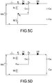
- FIG. 5A to FIG. 5D show schematic circuit diagrams of the FCC operating under states of duty cycle less than 0.5.
- the DC output voltage of the flying capacitor converter is controlled by controlling (turning on/off) the first switch S1 and the second switch S2, and therefore four states are implemented as shown in FIG. 5A (the first switch S1 is turned on and the second switch S2 is turned off), in FIG. 5B (the first switch S1 is turned off and the second switch S2 is turned off), in FIG. 5C (the first switch S1 is turned off and the second switch S2 is turned on), and in FIG. 5D (the first switch S1 is turned off and the second switch S2 is turned off).
- the first switch S1 In the first state, the first switch S1 is turned on and the second switch S2 is turned off as shown in FIG. 5A .
- the first switch S1 When the first switch S1 is turned on, the DC input voltage Vdc charges the inductor L, and a charging path is provided by the DC input voltage Vdc, the inductor L, the first switch S1, the flying capacitor C F1 , the second diode D2, the first capacitor C B1 , and the second capacitor C B2 .
- the flying capacitor C F1 is in a discharged state.
- the first switch S1 is turned off and the second switch S2 is turned off as shown in FIG. 5B . Since it will continue to keep the current flowing through the inductor L, a freewheel path is provided by the inductor L, the first diode D1, the second diode D2, the first capacitor C B1 , the second capacitor C B2 , and the DC input voltage Vdc.
- the freewheel path is an energy-releasing path of the inductor L.
- the first switch S1 is turned off and the second switch S2 is turned on as shown in FIG. 5C .
- the DC input voltage Vdc charges the inductor L, and a charging path is provided by the DC input voltage Vdc, the inductor L, the first diode D1, the flying capacitor C F1 , and the second switch S2.
- the inductor L and the flying capacitor C F1 are in an energy-storing state.
- the first switch S1 is turned off and the second switch S2 is turned off as shown in FIG. 5D .
- the inductor L is in the energy-releasing state, and an energy-releasing path is provided by the inductor L, the first diode D1, the second diode D2, the first capacitor C B1 , the second capacitor C B2 , and the DC input voltage Vdc.
- FIG. 6A to FIG. 6D show schematic circuit diagrams of the FCC operating under states of duty cycle greater than 0.5.
- the DC output voltage of the flying capacitor converter is controlled by controlling (turning on/off) the first switch S1 and the second switch S2, and therefore four states are implemented as shown in FIG. 6A (the first switch S1 is turned on and the second switch S2 is turned on), in FIG. 6B (the first switch S1 is turned off and the second switch S2 is turned on), in FIG. 6C (the first switch S1 is turned on and the second switch S2 is turned on), and in FIG. 6D (the first switch S1 is turned on and the second switch S2 is turned off).
- the first switch S1 is turned on and the second switch S2 is turned on as shown in FIG. 6A .
- the DC input voltage Vdc stores energy to the inductor L, and an energy-storing path is provided by the DC input voltage Vdc, the inductor L, the first switch S1, and the second switch S2.
- the first switch S1 is turned off and the second switch S2 is turned on as shown in FIG. 6B . Since it will continue to keep the current flowing through the inductor L, a freewheel path is provided by the inductor L, the first diode D1, the flying capacitor C F1 , and the second switch S2.
- the first switch S1 is turned on and the second switch S2 is turned on as shown in FIG. 6C .
- the DC input voltage Vdc stores energy to the inductor L, and an energy-storing path is provided by the DC input voltage Vdc, the inductor L, the first switch S1, and the second switch S2.
- the first switch S1 is turned on and the second switch S2 is turned off as shown in FIG. 6D . Since it will continue to keep the current flowing through the inductor L, a freewheel path is provided by the inductor L, the first switch S1, the flying capacitor C F1 , the second diode D2, the first capacitor C B1 , and the second capacitor C B2 .
- FIG. 7 shows a schematic circuit diagram of the FCC operating under unbalanced capacitor voltage.
- the voltage of the flying capacitor C F1 is controlled at half of the sum of the voltage of the first capacitor C B1 and the voltage of the second capacitor C B2 . If the voltage of the first capacitor C B1 is equal to the voltage of the second capacitor C B2 , no large charging current generates.
- the voltage ripple on the first capacitor C B1 and the second capacitor C B2 since the different states alternatively change as mentioned above.
- the voltage of the second capacitor C B2 is greater than the voltage of the flying capacitor C F1 , a charging path shown in FIG. 7 is formed.
- the connection position of the transient voltage suppressor TVS and the fifth diode D C3 is not limited to that shown in FIG. 7 , and as long as the two are coupled in series between the node P C and the node P D .
- FIG. 8 shows a circuit diagram of the flying capacitor converter according to a first preferred embodiment of the present disclosure.
- the FCC includes an inductor L, a first switch S1, a second switch S2, a first diode D1, a second diode D2, a third diode D C1 , a fourth diode D C2 , a fifth diode D C3 , a flying capacitor C F1 , a first capacitor C B1 , a second capacitor C B2 , a third capacitor Cc, and a transient voltage suppressor TVS.
- the transient voltage suppressor TVS may be replaced by a Zener diode.
- a first end of the inductor L is coupled to a positive end of a DC input voltage Vdc, and a second end of the inductor L is coupled to an anode of the first diode D1.
- the first switch S1 is coupled in series to the second switch S2, and a second end of the first switch S1 and a first end of the second switch S2 are commonly coupled to a node P S .
- a first end of the first switch S1, the second end of the inductor L, and the anode of the first diode D1 are commonly coupled to a node P L .
- a second end of the second switch S2 is coupled to a negative end of the DC input voltage Vdc.
- the first diode D1 is coupled in series to the second diode D2, and a cathode of the first diode D1 and an anode of the second diode D2 are commonly coupled to a node P D .
- the flying capacitor C F1 is coupled between the node P D and the node P S .
- the first capacitor C B1 is coupled in series to the second capacitor C B2 .
- a second end of the first capacitor C B1 and a first end of the second capacitor C B2 are commonly coupled to a node P C .
- a first end of the first capacitor C B1 is coupled to a cathode of the second diode D2, and a second end of the second capacitor C B2 is coupled to a negative end of the DC input voltage Vdc.
- An output of the FCC which is the first capacitor C B1 and the second capacitor C B2 , is coupled to a load.
- a voltage of the first capacitor C B1 is substantially equal to a voltage of the second capacitor C B2 .
- the voltage of the first capacitor C B1 is equal to the voltage of the second capacitor C B2 .
- An anode of the third diode D C1 is coupled to the node Ps, and a cathode of the third diode D C1 is coupled to a first end of the third capacitor C C , that is, the cathode of the third diode D C1 and the first end of the third capacitor C C are commonly coupled to a node P E .
- a second end of the third capacitor C C is coupled to the negative end of the DC input voltage Vdc.
- An anode of the fourth diode D C2 is coupled to the node P E , and a cathode of the fourth diode D C2 is coupled to the cathode of the second diode D2 and the first end of the first capacitor C B1 .
- An anode of the fifth diode D C3 is coupled to the node P C , and a cathode of the fifth diode D C3 is coupled to a first end of the transient voltage suppressor TVS, that is, the fifth diode D C3 and the transient voltage suppressor TVS are commonly coupled to a node P A .
- a second end of the transient voltage suppressor TVS is coupled to the node P D .
- the voltage of the first capacitor C B1 and the voltage of the second capacitor C B2 are 750 volts, respectively, and the voltage (breakdown voltage) of the transient voltage suppressor TVS is selected to be 100 volts. Since the voltage of the flying capacitor C F1 is controlled at half of the bus voltage, i.e., at half of the sum of the voltage of the first capacitor C B1 and the voltage of the second capacitor C B2 , the transient voltage suppressor TVS will not be turned on unless the voltage at the node P A is greater than 850 volts. In particular, the selection of the transient voltage suppressor TVS needs to consider the ripple voltage of the first capacitor C B1 and the ripple voltage of the voltage of the second capacitor C B2 .
- the transient voltage suppressor TVS is used to solve the problem of the withstand voltage of the second diode D2 by a charging path formed by the fifth diode D C3 , the transient voltage suppressor TVS, the flying capacitor C F1 , the third diode D C1 , the third capacitor C C , and the second capacitor C B2 when two flying capacitor converters are used in parallel and the DC input voltage Vdc does not supply power.
- the flying capacitor converter normally operates, it is to avoid excessive current frequently flowing through the fifth diode D C3 due to the charging path formed by the ripples.
- FIG. 11 shows a ripple waveform of a bus capacitor according to the present disclosure.
- a breakdown voltage of the transient voltage suppressor TVS can be considered (satisfied) according to the following relationship, and also refer to FIG. 4 .
- V TVS represents the breakdown voltage of the transient voltage suppressor TVS
- ⁇ VC B2 represents the ripple voltage of the second capacitor C B2
- ⁇ VC F1 represents the ripple voltage of the flying capacitor C F1
- Coe represents a coefficient value.
- the breakdown voltage of the transient voltage suppressor TVS is at least greater than a difference value between the maximum (peak) ripple voltage of the second capacitor C B2 and the minimum (valley) ripple voltage of the flying capacitor C F1 .
- the voltage of the flying capacitor C F1 would be close to the voltage of the first capacitor C B1 and the voltage of the second capacitor C B2 . Due to the ripple on the capacitor, actually the voltage of the second capacitor C B2 may be greater than the voltage of the flying capacitor C F1 .
- a current flowing through the second capacitor C B2 , the fifth diode D C3 , the flying capacitor C F1 , the second switch S2, and the second capacitor C B2 easily causes damage to the fifth diode D C3 . Therefore, the transient voltage suppressor TVS having an appropriate breakdown voltage can be added to protect the fifth diode D C3 .
- FIG. 10 shows a circuit diagram of the flying capacitor converter according to a second preferred embodiment of the present disclosure.
- the FCC further a first resistor R1.
- the first resistor R1 is coupled between the node P A and a node P B .
- the node P B is a common node of the second diode D2 and the fourth diode D C2 .
- the effect of the first resistor R1 is to charge the flying capacitor C F1 and the third capacitor C C by a current path shown in FIG. 10 when the first capacitor C B1 and the second capacitor C B2 can provide electrical energy but the DC input voltage Vdc fails to supply power.
- the current path is independent of the second capacitor C B2 , the fifth diode D C3 , and the transient voltage suppressor TVS, the damage of the fifth diode D C3 can be avoided.
Landscapes
- Engineering & Computer Science (AREA)
- Power Engineering (AREA)
- Dc-Dc Converters (AREA)
Abstract
Description
- The present disclosure relates to a flying capacitor converter, and more particularly to charging and circuit protection mechanisms for a flying capacitor converter.
- The statements in this section merely provide background information related to the present disclosure and do not necessarily constitute prior art.
- Please refer to
FIG. 1 , which shows a circuit diagram of a conventional flying capacitor converter (FCC). The FCC is essentially a DC-to-DC boost converter for stepping up a DC input voltage to a DC output voltage. The FCC includes an inductor L, a first switch S1, a second switch S2, a first diode D1, a second diode D2, a flying capacitor CF1, and an output capacitor C. The first switch S1 is coupled in series to the second switch S2, and commonly connected at a node PS. The first diode D1 is coupled in series to the second diode D2, and commonly connected at a node PD. The flying capacitor CF1 is coupled between the node PS and the node PD. In particular, the DC output voltage is controlled by turning on and turning off the first switch S1 and the second switch S2. - A first end of the inductor L is coupled to a positive end of a DC input voltage Vdc, and a second end of the inductor L is coupled to an anode of the first diode D1. The first switch S1 is coupled in series to the second switch S2, and a second end of the first switch S1 and a first end of the second switch S2 are commonly coupled to the node PS. A first end of the first switch S1, the second end of the inductor L, and the anode of the first diode D1 are commonly coupled to a node PL. A second end of the second switch S2 is coupled to a negative end of the DC input voltage Vdc.
- The first diode D1 is coupled in series to the second diode D2, and a cathode of the first diode D1 and an anode of the second diode D2 are commonly coupled to a node PD. The flying capacitor CF1 is coupled between the node PD and the node PS. A first end of the output capacitor C is coupled to a cathode of the second diode D2, and a second end of the output capacitor C is coupled to the negative end of the DC input voltage Vdc. An output that is the output capacitor C of the FCC is coupled to a load. The output capacitor C is for illustration only, and may actually consist of multiple capacitors connected in series and/or in parallel.
- However, the conventional flying capacitor converter has following disadvantages or problems: (1) the problem of the withstand voltage of the second switch S2, and (2) the problem of the withstand voltage of the second diode D2.
- An object of the present disclosure is to provide a flying capacitor converter to solve the problems of the related art.
- In order to achieve the above-mentioned object, the flying capacitor converter receives a DC input voltage and converts the DC input voltage into a DC output voltage. The flying capacitor converter includes an inductor, a first switch and a second switch, a first diode and a second diode, a first capacitor and a second capacitor, a flying capacitor, a third diode and a third capacitor, a fourth diode, and a fifth diode. The inductor is coupled between a positive end of the DC input voltage and a first node. The first switch and the second switch are commonly coupled to a second node, and the first switch is coupled to the first node and the second switch is coupled to a negative end of the DC input voltage. The first diode and the second diode are commonly coupled to a third node, and the first diode is coupled to the first node. The first capacitor and the second capacitor are commonly coupled to a fourth node, and the first capacitor is coupled to the second diode and the second capacitor is coupled to the second switch and the negative end of the DC input voltage. The first capacitor and the second capacitor provide the DC output voltage, and the fourth node is a midpoint of the DC output voltage. The flying capacitor is coupled to the second node and the third node. The third diode and the third capacitor are commonly coupled to a fifth node, and the third diode is coupled to the second node and the third capacitor is coupled to the second switch and the negative end of the DC input voltage. The fourth diode is coupled to the second diode and the fifth node. The fifth diode is coupled to the third node and the fourth node.
- In one embodiment, the flying capacitor converter further includes a voltage suppressor. The voltage suppressor is coupled in series to the fifth diode, and the voltage suppressor and the fifth diode are coupled between the third node and the fourth node.
- In one embodiment, the voltage suppressor and the fifth diode are commonly coupled to a sixth node, and the voltage suppressor is coupled to the third node and the fifth diode is coupled to the fourth node.
- In one embodiment, the flying capacitor converter further includes a first resistor. The first resistor is coupled between the sixth node and a seventh node. The seventh node is a common node of the second diode and the fourth diode.
- In one embodiment, when the DC input voltage initially supplies power, the first switch and the second switch are turned off, and the DC input voltage charges the first capacitor and the second capacitor and charges the flying capacitor and the third capacitor so that a voltage ratio between the first switch and the second switch is substantially equal to a voltage ratio between the flying capacitor and the third capacitor.
- In one embodiment, an output of the flying capacitor converter is coupled to an output of a second flying capacitor converter, and the second flying capacitor converter converts a second DC input voltage into a second DC output voltage.
- In one embodiment, a breakdown voltage of the voltage suppressor is greater than a difference between a maximum ripple voltage of the second capacitor and a minimum ripple voltage of the flying capacitor.
- In one embodiment, at a predetermined time before the flying capacitor converter active, the flying capacitor converter provides a control signal with an extremely small duty cycle to the second switch so that the flying capacitor is slowly charged.
- In one embodiment, the voltage suppressor is a transient voltage suppressor or a Zener diode.
- Accordingly, the flying capacitor converter provides charging and circuit protection mechanisms.
- It is to be understood that both the foregoing general description and the following detailed description are exemplary, and are intended to provide further explanation of the present disclosure as claimed. Other advantages and features of the present disclosure will be apparent from the following description, drawings and claims.
- The present disclosure can be more fully understood by reading the following detailed description of the embodiment, with reference made to the accompanying drawing as follows:
-
FIG. 1 is a circuit diagram of a conventional flying capacitor converter (FCC). -
FIG. 2 is a circuit diagram of a first embodiment of an improved FCC. -
FIG. 3 is a circuit diagram of the first embodiment of the improved FCC used in parallel. -
FIG. 4 is a circuit diagram of a second embodiment of the improved FCC. -
FIG. 5A to FIG. 5D are schematic circuit diagrams of the FCC operating under states of duty cycle less than 0.5. -
FIG. 6A to FIG. 6D are schematic circuit diagrams of the FCC operating under states of duty cycle greater than 0.5. -
FIG. 7 is a schematic circuit diagram of the FCC operating under unbalanced capacitor voltage. -
FIG. 8 is a circuit diagram of the flying capacitor converter according to a first preferred embodiment of the present disclosure. -
FIG. 9 is a schematic circuit diagram illustrating a protection current of the flying capacitor converter according to the first preferred embodiment of the present disclosure. -
FIG. 10 is a circuit diagram of the flying capacitor converter according to a second preferred embodiment of the present disclosure. -
FIG. 11 is a ripple waveform of a bus capacitor according to the present disclosure. - Reference will now be made to the drawing figures to describe the present disclosure in detail. It will be understood that the drawing figures and exemplified embodiments of present disclosure are not limited to the details thereof.
- As mentioned above, the flying capacitor converter of the present disclosure is provided to solve the problems: (1) the problem of the withstand voltage of the second switch S2, and (2) the problem of the withstand voltage of the second diode D2.
- (1) the problem of the withstand voltage of the second switch S2: when the DC input voltage Vdc starts to supply power, thereby charging the output capacitor through the inductor L, the first diode D1, and the second diode D2. Since the flying capacitor CF1 has no charging path yet, a voltage across the flying capacitor CF1 is close to zero, and a voltage across the second switch S2 is close to the magnitude of the DC input voltage Vdc. Therefore, the withstand voltage problem of the second switch S2 will be caused.
Please refer toFIG. 2 , which shows a circuit diagram of a first embodiment of an improved FCC. In order to solve the withstand voltage problem of the second switch S2 caused by the DC input voltage Vdc starting to supply power, a third capacitor CC, a third diode DC1, and a fourth diode DC2 are provided. Here, the output capacitor is represented by a first capacitor CB1 and a second capacitor CB2 connected in series. Specifically, a cathode of the third diode DC1 is coupled to an anode of the fourth diode DC2 and one end of the third capacitor CC, that is, the third diode DC1, the fourth diode DC2, and the third capacitor CC are commonly coupled to a node PE. An anode of the third diode DC1 is coupled to the node PS, a cathode of the fourth diode DC2 is coupled to the second diode D2 and the firs capacitor CB1, and the other end of the third capacitor CC is coupled to the second switch S2 and the second capacitor CB2. Therefore, when the DC input voltage Vdc starts to supply power, not only the first capacitor CB1 and the second capacitor CB2 are charged through the inductor L, the first diode D1, and the second diode D2, but also the third capacitor CC is charged through the inductor L, the first diode D1, the flying capacitor CF1, and the third diode DC1. Therefore, an effect of voltage division is provided so that a voltage ratio between the first switch S1 and the second switch S2 is equal to a voltage ratio between the flying capacitor CF1 and the third capacitor CC, thereby solving the withstand voltage problem of the second switch S2. Moreover, the fourth diode DC2 provides a discharging path when the third capacitor CC discharges. - (2) the problem of the withstand voltage of the second diode D2: as shown in
FIG. 3 , which shows a circuit diagram of the first embodiment of the improved FCC used in parallel. Under the condition that two flying capacitor converters are used in parallel, when the DC input voltage Vdc does not supply power and the other DC input voltage Vdc' (a second DC input voltage) provides a DC high voltage (for example, but not limited to 1500 volts), the sum of the voltage of the first capacitor CB1 and the voltage of the second capacitor CB2 is equivalent to the magnitude of the DC high voltage. For the second diode D2, it is equivalent to withstand the reverse bias voltage of the DC high voltage, thereby causing the problem of the withstand voltage of the second diode D2. In practical applications, it is not easy to obtain the second diode D2 with such a high withstand voltage. Furthermore, even if a diode with such a high withstand voltage can be obtained for use, or by connecting multiple diodes in series, it will cause the problem with poor efficiency. - In order to solve the above-mentioned problem, as shown in
FIG. 4 , which shows a circuit diagram of a second embodiment of the improved FCC. In order to solve the withstand voltage problem of the second diode D2 caused by the DC input voltage Vdc' providing the DC high voltage but the DC input voltage Vdc supplying no power, a fifth diode DC3 and a transient voltage suppressor TVS are provided, and also a fifth diode DC3' and a transient voltage suppressor TVS' are provided. Specifically, the transient voltage suppressor TVS is coupled in series to the fifth diode DC3, and commonly coupled to a node PA. The other end of the transient voltage suppressor TVS is coupled to the node PD, and an anode of the fifth diode DC3 is coupled to a common node PC between the first capacitor CB1 and the second capacitor CB2. - When the DC input voltage Vdc does not yet supply power and the DC input voltage Vdc' provides the DC high voltage, the DC high voltage will charge the first capacitor CB1 and the second capacitor CB2, and therefore a voltage across the second capacitor CB2 is approximately equal to half of the DC high voltage. At this condition, a voltage at a midpoint, i.e., the node PC of the first capacitor CB1 and the second capacitor CB2 will produce a charging path, and the charging path is provided by the fifth diode DC3, the transient voltage suppressor TVS, the flying capacitor CF1, the third diode DC1, the third capacitor CC, and the second capacitor CB2. In particular, an electric potential of the anode of the second diode D2 is about half of the magnitude of the DC high voltage minus the voltage of the transient voltage suppressor TVS. Therefore, the voltage across the second diode D2 is half of the magnitude of the DC high voltage plus the voltage of the transient voltage suppressor TVS, that is, the withstand voltage of the second diode D2 does not need to reach the magnitude of the DC high voltage, thereby solving the problem of the withstand voltage of the second diode D2. In particular, the first capacitor CB1 and the second capacitor CB2 are not limited to only two independent capacitors, but may also be composed of multiple capacitors, and the node PC is a voltage midpoint, that is, the voltage of the node PC is approximately equal to half of the output voltage. The selection of the midpoint can be achieved by selecting the first capacitor CB1 and the second capacitor CB2 to have the same capacitance value, or controlling the voltage of the node PC to be equal to half of the output voltage by a power conversion apparatus when the load connected to the output voltage is the power conversion apparatus such as an inverter.
- Please refer to
FIG. 5A to FIG. 5D , which show schematic circuit diagrams of the FCC operating under states of duty cycle less than 0.5. The DC output voltage of the flying capacitor converter is controlled by controlling (turning on/off) the first switch S1 and the second switch S2, and therefore four states are implemented as shown inFIG. 5A (the first switch S1 is turned on and the second switch S2 is turned off), inFIG. 5B (the first switch S1 is turned off and the second switch S2 is turned off), inFIG. 5C (the first switch S1 is turned off and the second switch S2 is turned on), and inFIG. 5D (the first switch S1 is turned off and the second switch S2 is turned off). - In the first state, the first switch S1 is turned on and the second switch S2 is turned off as shown in
FIG. 5A . When the first switch S1 is turned on, the DC input voltage Vdc charges the inductor L, and a charging path is provided by the DC input voltage Vdc, the inductor L, the first switch S1, the flying capacitor CF1, the second diode D2, the first capacitor CB1, and the second capacitor CB2. The flying capacitor CF1 is in a discharged state. - In the second state, the first switch S1 is turned off and the second switch S2 is turned off as shown in
FIG. 5B . Since it will continue to keep the current flowing through the inductor L, a freewheel path is provided by the inductor L, the first diode D1, the second diode D2, the first capacitor CB1, the second capacitor CB2, and the DC input voltage Vdc. In particular, the freewheel path is an energy-releasing path of the inductor L. - In the third state, the first switch S1 is turned off and the second switch S2 is turned on as shown in
FIG. 5C . The DC input voltage Vdc charges the inductor L, and a charging path is provided by the DC input voltage Vdc, the inductor L, the first diode D1, the flying capacitor CF1, and the second switch S2. The inductor L and the flying capacitor CF1 are in an energy-storing state. - In the fourth state, the first switch S1 is turned off and the second switch S2 is turned off as shown in
FIG. 5D . At this condition, the inductor L is in the energy-releasing state, and an energy-releasing path is provided by the inductor L, the first diode D1, the second diode D2, the first capacitor CB1, the second capacitor CB2, and the DC input voltage Vdc. - Please refer to
FIG. 6A to FIG. 6D , which show schematic circuit diagrams of the FCC operating under states of duty cycle greater than 0.5. The DC output voltage of the flying capacitor converter is controlled by controlling (turning on/off) the first switch S1 and the second switch S2, and therefore four states are implemented as shown inFIG. 6A (the first switch S1 is turned on and the second switch S2 is turned on), inFIG. 6B (the first switch S1 is turned off and the second switch S2 is turned on), inFIG. 6C (the first switch S1 is turned on and the second switch S2 is turned on), and inFIG. 6D (the first switch S1 is turned on and the second switch S2 is turned off). - In the first state, the first switch S1 is turned on and the second switch S2 is turned on as shown in
FIG. 6A . The DC input voltage Vdc stores energy to the inductor L, and an energy-storing path is provided by the DC input voltage Vdc, the inductor L, the first switch S1, and the second switch S2. - In the second state, the first switch S1 is turned off and the second switch S2 is turned on as shown in
FIG. 6B . Since it will continue to keep the current flowing through the inductor L, a freewheel path is provided by the inductor L, the first diode D1, the flying capacitor CF1, and the second switch S2. - In the third state, the first switch S1 is turned on and the second switch S2 is turned on as shown in
FIG. 6C . The DC input voltage Vdc stores energy to the inductor L, and an energy-storing path is provided by the DC input voltage Vdc, the inductor L, the first switch S1, and the second switch S2. - In the fourth state, the first switch S1 is turned on and the second switch S2 is turned off as shown in
FIG. 6D . Since it will continue to keep the current flowing through the inductor L, a freewheel path is provided by the inductor L, the first switch S1, the flying capacitor CF1, the second diode D2, the first capacitor CB1, and the second capacitor CB2. - Please refer to
FIG. 7 , which shows a schematic circuit diagram of the FCC operating under unbalanced capacitor voltage. Basically, the voltage of the flying capacitor CF1 is controlled at half of the sum of the voltage of the first capacitor CB1 and the voltage of the second capacitor CB2. If the voltage of the first capacitor CB1 is equal to the voltage of the second capacitor CB2, no large charging current generates. During the operation of the flying capacitor converter, there is voltage ripple on the first capacitor CB1 and the second capacitor CB2 since the different states alternatively change as mentioned above. When the voltage of the second capacitor CB2 is greater than the voltage of the flying capacitor CF1, a charging path shown inFIG. 7 is formed. By adding the transient voltage suppressor TVS to the charging path, the sum of the voltage of the flying capacitor CF1 and the voltage of the transient voltage suppressor TVS is greater than the voltage of the second capacitor CB2 to avoid current flowing through this charging path. Therefore, the voltage selection of the transient voltage suppressor TVS can be determined according to this principle to avoid forming the charging path shown inFIG. 7 due to ripples, thereby protecting the fifth diode DC3. Accordingly, it is to avoid excessive current frequently flowing through the fifth diode DC3 during the operation of the flying capacitor converter. The connection position of the transient voltage suppressor TVS and the fifth diode DC3 is not limited to that shown inFIG. 7 , and as long as the two are coupled in series between the node PC and the node PD. - Please refer to
FIG. 8 , which shows a circuit diagram of the flying capacitor converter according to a first preferred embodiment of the present disclosure. When the DC input voltage Vdc starts to supply power, at a predetermined time before the flying capacitor converter activates, that is, at a predetermined time before the first switch S1 and the second switch S2 start to operate shown inFIG. 5A to FIG. 5D orFIG. 6A to FIG. 6D , a control signal with an extremely small duty cycle is provided to the second switch S2 so that the flying capacitor CF1 is slowly charged until the sum of the voltage of the flying capacitor CF1 and the voltage of the transient voltage suppressor TVS is equal to the voltage of the second capacitor CB2. - Please refer to
FIG. 8 again, the FCC includes an inductor L, a first switch S1, a second switch S2, a first diode D1, a second diode D2, a third diode DC1, a fourth diode DC2, a fifth diode DC3, a flying capacitor CF1, a first capacitor CB1, a second capacitor CB2, a third capacitor Cc, and a transient voltage suppressor TVS. In particular, the transient voltage suppressor TVS may be replaced by a Zener diode. - A first end of the inductor L is coupled to a positive end of a DC input voltage Vdc, and a second end of the inductor L is coupled to an anode of the first diode D1. The first switch S1 is coupled in series to the second switch S2, and a second end of the first switch S1 and a first end of the second switch S2 are commonly coupled to a node PS. A first end of the first switch S1, the second end of the inductor L, and the anode of the first diode D1 are commonly coupled to a node PL. A second end of the second switch S2 is coupled to a negative end of the DC input voltage Vdc.
- The first diode D1 is coupled in series to the second diode D2, and a cathode of the first diode D1 and an anode of the second diode D2 are commonly coupled to a node PD. The flying capacitor CF1 is coupled between the node PD and the node PS. The first capacitor CB1 is coupled in series to the second capacitor CB2. A second end of the first capacitor CB1 and a first end of the second capacitor CB2 are commonly coupled to a node PC. A first end of the first capacitor CB1 is coupled to a cathode of the second diode D2, and a second end of the second capacitor CB2 is coupled to a negative end of the DC input voltage Vdc. An output of the FCC, which is the first capacitor CB1 and the second capacitor CB2, is coupled to a load. In particular, a voltage of the first capacitor CB1 is substantially equal to a voltage of the second capacitor CB2. In an ideal condition, that is, without considering the ripple voltage, the voltage of the first capacitor CB1 is equal to the voltage of the second capacitor CB2.
- An anode of the third diode DC1 is coupled to the node Ps, and a cathode of the third diode DC1 is coupled to a first end of the third capacitor CC, that is, the cathode of the third diode DC1 and the first end of the third capacitor CC are commonly coupled to a node PE. A second end of the third capacitor CC is coupled to the negative end of the DC input voltage Vdc. An anode of the fourth diode DC2 is coupled to the node PE, and a cathode of the fourth diode DC2 is coupled to the cathode of the second diode D2 and the first end of the first capacitor CB1. An anode of the fifth diode DC3 is coupled to the node PC, and a cathode of the fifth diode DC3 is coupled to a first end of the transient voltage suppressor TVS, that is, the fifth diode DC3 and the transient voltage suppressor TVS are commonly coupled to a node PA. A second end of the transient voltage suppressor TVS is coupled to the node PD.
- It is assumed that the voltage of the first capacitor CB1 and the voltage of the second capacitor CB2 are 750 volts, respectively, and the voltage (breakdown voltage) of the transient voltage suppressor TVS is selected to be 100 volts. Since the voltage of the flying capacitor CF1 is controlled at half of the bus voltage, i.e., at half of the sum of the voltage of the first capacitor CB1 and the voltage of the second capacitor CB2, the transient voltage suppressor TVS will not be turned on unless the voltage at the node PA is greater than 850 volts. In particular, the selection of the transient voltage suppressor TVS needs to consider the ripple voltage of the first capacitor CB1 and the ripple voltage of the voltage of the second capacitor CB2. Therefore, the transient voltage suppressor TVS is used to solve the problem of the withstand voltage of the second diode D2 by a charging path formed by the fifth diode DC3, the transient voltage suppressor TVS, the flying capacitor CF1, the third diode DC1, the third capacitor CC, and the second capacitor CB2 when two flying capacitor converters are used in parallel and the DC input voltage Vdc does not supply power. When the flying capacitor converter normally operates, it is to avoid excessive current frequently flowing through the fifth diode DC3 due to the charging path formed by the ripples.
- Please refer to
FIG. 11 , which shows a ripple waveform of a bus capacitor according to the present disclosure. A breakdown voltage of the transient voltage suppressor TVS can be considered (satisfied) according to the following relationship, and also refer toFIG. 4 . VTVS>(0.5×ΔVCB2+0.5×ΔVCF1)×Coe
where, VTVS represents the breakdown voltage of the transient voltage suppressor TVS, ΔVCB2 represents the ripple voltage of the second capacitor CB2, ΔVCF1 represents the ripple voltage of the flying capacitor CF1, and Coe represents a coefficient value. According to the relationship above, the breakdown voltage of the transient voltage suppressor TVS is at least greater than a difference value between the maximum (peak) ripple voltage of the second capacitor CB2 and the minimum (valley) ripple voltage of the flying capacitor CF1. - When the first switch S1 and the second switch S2 are controlled to be on/off, theoretically the voltage of the flying capacitor CF1 would be close to the voltage of the first capacitor CB1 and the voltage of the second capacitor CB2. Due to the ripple on the capacitor, actually the voltage of the second capacitor CB2 may be greater than the voltage of the flying capacitor CF1. At this condition, a current flowing through the second capacitor CB2, the fifth diode DC3, the flying capacitor CF1, the second switch S2, and the second capacitor CB2 easily causes damage to the fifth diode DC3. Therefore, the transient voltage suppressor TVS having an appropriate breakdown voltage can be added to protect the fifth diode DC3.
- Please refer to
FIG. 10 , which shows a circuit diagram of the flying capacitor converter according to a second preferred embodiment of the present disclosure. The FCC further a first resistor R1. The first resistor R1 is coupled between the node PA and a node PB. The node PB is a common node of the second diode D2 and the fourth diode DC2. The effect of the first resistor R1 is to charge the flying capacitor CF1 and the third capacitor CC by a current path shown inFIG. 10 when the first capacitor CB1 and the second capacitor CB2 can provide electrical energy but the DC input voltage Vdc fails to supply power. In particular, since the current path is independent of the second capacitor CB2, the fifth diode DC3, and the transient voltage suppressor TVS, the damage of the fifth diode DC3 can be avoided.
Claims (9)
- A flying capacitor converter configured to receive a DC input voltage (Vdc) and convert the DC input voltage (Vdc) into a DC output voltage, characterized in that the flying capacitor converter comprising:an inductor (L) coupled between a positive end of the DC input voltage (Vdc) and a first node (PL),a first switch (S1) and a second switch (S2) commonly coupled to a second node (PS), and the first switch (S1) coupled to the first node (PL) and the second switch (S2) coupled to a negative end of the DC input voltage (Vdc),a first diode (D1) and a second diode (D2) commonly coupled to a third node (PD), and the first diode (D1) coupled to the first node (PL),a first capacitor (CB1) and a second capacitor (CB2) commonly coupled to a fourth node (PC), and the first capacitor (CB1) coupled to the second diode (D2) and the second capacitor (CB2) coupled to the second switch (S2) and the negative end of the DC input voltage (Vdc), wherein the first capacitor (CB1) and the second capacitor (CB2) are configured to provide the DC output voltage, and the fourth node (PC) is a midpoint of the DC output voltage,a flying capacitor (CF1) coupled to the second node (PS) and the third node (PD),a third diode (DC1) and a third capacitor (CC) commonly coupled to a fifth node (PE), and the third diode (DC1) coupled to the second node (PS) and the third capacitor (CC) coupled to the second switch (S2) and the negative end of the DC input voltage (Vdc),a fourth diode (DC2) coupled to the second diode (D2) and the fifth node (PE), anda fifth diode (DC3) coupled to the third node (PD) and the fourth node (PC).
- The flying capacitor converter in claim 1, further comprising:
a voltage suppressor (TVS) coupled in series to the fifth diode (DC3), and the voltage suppressor (TVS) and the fifth diode (DC3) coupled between the third node (PD) and the fourth node (PC). - The flying capacitor converter in claim 2, wherein the voltage suppressor (TVS) and the fifth diode (DC3) are commonly coupled to a sixth node (PA), and the voltage suppressor (TVS) is coupled to the third node (PD) and the fifth diode (DC3) is coupled to the fourth node (PC).
- The flying capacitor converter in claim 3, further comprising:
a first resistor (R1) coupled between the sixth node (PA) and a seventh node (PB), wherein the seventh node (PB) is a common node of the second diode (D2) and the fourth diode (DC2). - The flying capacitor converter in claim 1, wherein when the DC input voltage (Vdc) initially supplies power, the first switch (S1) and the second switch (S2) are turned off, and the DC input voltage (Vdc) charges the first capacitor (CB1) and the second capacitor (CB2) and charges the flying capacitor (CF1) and the third capacitor (CC) so that a voltage ratio between the first switch (S1) and the second switch (S2) is substantially equal to a voltage ratio between the flying capacitor (CF1) and the third capacitor (CC).
- The flying capacitor converter in claim 2, wherein an output of the flying capacitor converter is coupled to an output of a second flying capacitor converter, and the second flying capacitor converter is configured to convert a second DC input voltage into a second DC output voltage.
- The flying capacitor converter in claim 2, wherein a breakdown voltage of the voltage suppressor (TVS) is greater than a difference between a maximum ripple voltage of the second capacitor (CB2) and a minimum ripple voltage of the flying capacitor (CF1).
- The flying capacitor converter in claim 2, wherein at a predetermined time before the flying capacitor converter actives, the flying capacitor converter provides a control signal with an extremely small duty cycle to the second switch (S2) so that the flying capacitor (CF1) is slowly charged.
- The flying capacitor converter in claim 2, wherein the voltage suppressor (TVS) is a transient voltage suppressor or a Zener diode.
Applications Claiming Priority (2)
| Application Number | Priority Date | Filing Date | Title |
|---|---|---|---|
| US201962892843P | 2019-08-28 | 2019-08-28 | |
| US16/868,873 US11362589B2 (en) | 2019-08-28 | 2020-05-07 | Flying capacitor converter |
Publications (3)
| Publication Number | Publication Date |
|---|---|
| EP3787167A1 true EP3787167A1 (en) | 2021-03-03 |
| EP3787167C0 EP3787167C0 (en) | 2024-05-29 |
| EP3787167B1 EP3787167B1 (en) | 2024-05-29 |
Family
ID=70736709
Family Applications (1)
| Application Number | Title | Priority Date | Filing Date |
|---|---|---|---|
| EP20174658.3A Active EP3787167B1 (en) | 2019-08-28 | 2020-05-14 | Flying capacitor converter |
Country Status (6)
| Country | Link |
|---|---|
| US (1) | US11362589B2 (en) |
| EP (1) | EP3787167B1 (en) |
| JP (1) | JP7026737B2 (en) |
| CN (1) | CN112448580B (en) |
| ES (1) | ES2983952T3 (en) |
| TW (1) | TWI727789B (en) |
Families Citing this family (2)
| Publication number | Priority date | Publication date | Assignee | Title |
|---|---|---|---|---|
| US11201562B1 (en) * | 2019-06-23 | 2021-12-14 | Purdue Research Foundation | Soft-switching voltage-edge-rate-limiting power inverter |
| GB2591800B (en) * | 2020-02-07 | 2026-02-18 | Pulsiv Ltd | Electrical conversion |
Citations (4)
| Publication number | Priority date | Publication date | Assignee | Title |
|---|---|---|---|---|
| US20130021011A1 (en) * | 2010-02-01 | 2013-01-24 | Mitsubishi Electric Corporation | Dc/dc power conversion apparatus |
| DE102014109048A1 (en) * | 2014-06-27 | 2015-12-31 | Sma Solar Technology Ag | Multi-level half-bridge arrangement, voltage converter and circuit arrangement with such a half-bridge arrangement and method for operating a voltage converter |
| CN108923632A (en) * | 2018-08-29 | 2018-11-30 | 阳光电源股份有限公司 | A kind of more level BOOST devices |
| CN109039061A (en) * | 2018-08-29 | 2018-12-18 | 阳光电源股份有限公司 | A kind of more level BOOST devices |
Family Cites Families (23)
| Publication number | Priority date | Publication date | Assignee | Title |
|---|---|---|---|---|
| US6538906B1 (en) * | 2002-02-11 | 2003-03-25 | Delta Electronics, Inc. | Energy storage circuit for DC-DC converter |
| TWI231088B (en) * | 2002-11-14 | 2005-04-11 | Int Rectifier Corp | Control IC for low power auxiliary supplies |
| EP2466738B1 (en) * | 2010-12-20 | 2018-04-04 | ams AG | Voltage converter and method for voltage conversion |
| JP5528622B2 (en) | 2011-04-15 | 2014-06-25 | 三菱電機株式会社 | DC / DC power converter and solar power generation system |
| JP5665649B2 (en) | 2011-05-12 | 2015-02-04 | 三菱電機株式会社 | DC / DC power converter |
| TWI433440B (en) * | 2011-07-08 | 2014-04-01 | Univ Nat Taipei Technology | High boost converter |
| US8946931B2 (en) * | 2011-07-28 | 2015-02-03 | Schneider Electric It Corporation | Dual boost converter for UPS system |
| JP5642316B2 (en) | 2012-03-23 | 2014-12-17 | 三菱電機株式会社 | Power conditioner and photovoltaic power generation system |
| JP2014036491A (en) | 2012-08-08 | 2014-02-24 | Mitsubishi Electric Corp | Dc/dc power conversion device, and power conditioner for photovoltaic system |
| TWI477047B (en) * | 2013-01-21 | 2015-03-11 | Univ Nat Taipei Technology | High boost power conversion device |
| JP6355819B2 (en) | 2015-03-02 | 2018-07-11 | 三菱電機株式会社 | Power conversion device and refrigeration cycle device |
| US9806601B2 (en) * | 2015-03-27 | 2017-10-31 | Futurewei Technologies, Inc. | Boost converter and method |
| CN106230253B (en) * | 2016-09-09 | 2019-05-07 | 华为技术有限公司 | Boost power conversion circuit and control method |
| US10554128B2 (en) * | 2018-01-05 | 2020-02-04 | Futurewei Technologies, Inc. | Multi-level boost converter |
| CN108471235A (en) * | 2018-03-28 | 2018-08-31 | 江苏固德威电源科技股份有限公司 | The two-way DC/DC circuits of three level |
| DE102018206918B3 (en) * | 2018-05-04 | 2019-10-31 | Dialog Semiconductor (Uk) Limited | Hybrid buck-boost converter |
| CN108847769B (en) * | 2018-06-22 | 2020-03-24 | 阳光电源股份有限公司 | A three-level boost device and its control method |
| CN108900078B (en) * | 2018-08-03 | 2020-07-07 | 阳光电源股份有限公司 | A flying capacitor type three-level converter and its control method |
| CN109756115B (en) * | 2018-12-21 | 2021-12-03 | 华为数字技术(苏州)有限公司 | Boost power conversion circuit, method, inverter, device and system |
| US10790742B1 (en) * | 2019-04-17 | 2020-09-29 | Dialog Semiconductor (Uk) Limited | Multi-level power converter with improved transient load response |
| CN110165888B (en) | 2019-06-11 | 2024-05-14 | 阳光电源股份有限公司 | Three-level Boost circuit and multi-output parallel system |
| US10985653B1 (en) * | 2020-03-20 | 2021-04-20 | Infineon Technologies Ag | Charge pump converter and control method |
| CN111277131A (en) * | 2020-03-27 | 2020-06-12 | 宁波锦浪新能源科技股份有限公司 | A booster power conversion circuit and its control method |
-
2020
- 2020-05-07 US US16/868,873 patent/US11362589B2/en active Active
- 2020-05-11 TW TW109115539A patent/TWI727789B/en active
- 2020-05-11 CN CN202010393347.2A patent/CN112448580B/en active Active
- 2020-05-14 ES ES20174658T patent/ES2983952T3/en active Active
- 2020-05-14 EP EP20174658.3A patent/EP3787167B1/en active Active
- 2020-07-09 JP JP2020118535A patent/JP7026737B2/en active Active
Patent Citations (6)
| Publication number | Priority date | Publication date | Assignee | Title |
|---|---|---|---|---|
| US20130021011A1 (en) * | 2010-02-01 | 2013-01-24 | Mitsubishi Electric Corporation | Dc/dc power conversion apparatus |
| DE102014109048A1 (en) * | 2014-06-27 | 2015-12-31 | Sma Solar Technology Ag | Multi-level half-bridge arrangement, voltage converter and circuit arrangement with such a half-bridge arrangement and method for operating a voltage converter |
| CN108923632A (en) * | 2018-08-29 | 2018-11-30 | 阳光电源股份有限公司 | A kind of more level BOOST devices |
| CN109039061A (en) * | 2018-08-29 | 2018-12-18 | 阳光电源股份有限公司 | A kind of more level BOOST devices |
| US20200076301A1 (en) * | 2018-08-29 | 2020-03-05 | Sungrow Power Supply Co., Ltd. | Multi-Level Boost Apparatus |
| US20200076302A1 (en) * | 2018-08-29 | 2020-03-05 | Sungrow Power Supply Co., Ltd. | Multi-Level Boost Apparatus |
Also Published As
| Publication number | Publication date |
|---|---|
| US11362589B2 (en) | 2022-06-14 |
| TW202110061A (en) | 2021-03-01 |
| CN112448580A (en) | 2021-03-05 |
| US20210067039A1 (en) | 2021-03-04 |
| TWI727789B (en) | 2021-05-11 |
| EP3787167C0 (en) | 2024-05-29 |
| EP3787167B1 (en) | 2024-05-29 |
| JP7026737B2 (en) | 2022-02-28 |
| JP2021035326A (en) | 2021-03-01 |
| CN112448580B (en) | 2022-03-01 |
| ES2983952T3 (en) | 2024-10-28 |
Similar Documents
| Publication | Publication Date | Title |
|---|---|---|
| CN106026619B (en) | Current-limiting peak value adjusting circuit, current-limiting unit, control circuit and power converter | |
| US9413230B2 (en) | Power converter | |
| US6538906B1 (en) | Energy storage circuit for DC-DC converter | |
| US11329569B2 (en) | Power conversion system | |
| US20250317060A1 (en) | Buck-boost converter and power supply system | |
| CN116260319B (en) | Power converter and power switch controller for power converter | |
| KR20090044137A (en) | Transformerless Boost Converter | |
| US12580489B2 (en) | DC/DC converter and control method thereof | |
| US11362589B2 (en) | Flying capacitor converter | |
| US11831238B2 (en) | Power conversion system | |
| CN113726175B (en) | Conversion device, controller and power supply control method thereof | |
| JP2006158073A (en) | Capacitor charge / discharge method and power converter | |
| Abosnina et al. | A novel three-phase bidirectional DC-DC converter for UPS applications | |
| US20230097921A1 (en) | Gate driver circuit for a power supply voltage converter | |
| CN111934554B (en) | Power supply conversion device | |
| CN116711172A (en) | DC-DC Converter | |
| EP3772806A1 (en) | Power converter | |
| EP3952081B1 (en) | Conversion apparatus with three-level switching circuit and method of operating the same | |
| KR102723818B1 (en) | High Step-Up Digital-Controlled DC Power Converter using the Clamping-Mode Boost Inductor and Its Control Method | |
| CN215120579U (en) | Switching power supply circuit, driving device and power electronic power switch | |
| KR102744736B1 (en) | Dc-dc converter | |
| US10965217B2 (en) | Power conversion apparatus | |
| JP2009005487A (en) | Power system | |
| SU1676034A1 (en) | Single-cycle d c-to-d c voltage converter | |
| KR20140115218A (en) | Power conversion apparatus, energy storage system and driving method of the same |
Legal Events
| Date | Code | Title | Description |
|---|---|---|---|
| PUAI | Public reference made under article 153(3) epc to a published international application that has entered the european phase |
Free format text: ORIGINAL CODE: 0009012 |
|
| STAA | Information on the status of an ep patent application or granted ep patent |
Free format text: STATUS: THE APPLICATION HAS BEEN PUBLISHED |
|
| AK | Designated contracting states |
Kind code of ref document: A1 Designated state(s): AL AT BE BG CH CY CZ DE DK EE ES FI FR GB GR HR HU IE IS IT LI LT LU LV MC MK MT NL NO PL PT RO RS SE SI SK SM TR |
|
| AX | Request for extension of the european patent |
Extension state: BA ME |
|
| STAA | Information on the status of an ep patent application or granted ep patent |
Free format text: STATUS: REQUEST FOR EXAMINATION WAS MADE |
|
| 17P | Request for examination filed |
Effective date: 20210903 |
|
| RBV | Designated contracting states (corrected) |
Designated state(s): AL AT BE BG CH CY CZ DE DK EE ES FI FR GB GR HR HU IE IS IT LI LT LU LV MC MK MT NL NO PL PT RO RS SE SI SK SM TR |
|
| STAA | Information on the status of an ep patent application or granted ep patent |
Free format text: STATUS: EXAMINATION IS IN PROGRESS |
|
| 17Q | First examination report despatched |
Effective date: 20220704 |
|
| REG | Reference to a national code |
Ref legal event code: R079 Free format text: PREVIOUS MAIN CLASS: H02M0003070000 Ref country code: DE Ref legal event code: R079 Ref document number: 602020031528 Country of ref document: DE Free format text: PREVIOUS MAIN CLASS: H02M0003070000 Ipc: H02M0001360000 |
|
| GRAP | Despatch of communication of intention to grant a patent |
Free format text: ORIGINAL CODE: EPIDOSNIGR1 |
|
| STAA | Information on the status of an ep patent application or granted ep patent |
Free format text: STATUS: GRANT OF PATENT IS INTENDED |
|
| RIC1 | Information provided on ipc code assigned before grant |
Ipc: H02M 1/32 20070101ALI20240215BHEP Ipc: H02M 3/158 20060101ALI20240215BHEP Ipc: H02M 3/07 20060101ALI20240215BHEP Ipc: H02M 7/483 20070101ALI20240215BHEP Ipc: H02M 1/36 20070101AFI20240215BHEP |
|
| INTG | Intention to grant announced |
Effective date: 20240229 |
|
| GRAS | Grant fee paid |
Free format text: ORIGINAL CODE: EPIDOSNIGR3 |
|
| GRAA | (expected) grant |
Free format text: ORIGINAL CODE: 0009210 |
|
| STAA | Information on the status of an ep patent application or granted ep patent |
Free format text: STATUS: THE PATENT HAS BEEN GRANTED |
|
| AK | Designated contracting states |
Kind code of ref document: B1 Designated state(s): AL AT BE BG CH CY CZ DE DK EE ES FI FR GB GR HR HU IE IS IT LI LT LU LV MC MK MT NL NO PL PT RO RS SE SI SK SM TR |
|
| REG | Reference to a national code |
Ref country code: CH Ref legal event code: EP |
|
| REG | Reference to a national code |
Ref country code: IE Ref legal event code: FG4D |
|
| REG | Reference to a national code |
Ref country code: DE Ref legal event code: R096 Ref document number: 602020031528 Country of ref document: DE |
|
| U01 | Request for unitary effect filed |
Effective date: 20240610 |
|
| U07 | Unitary effect registered |
Designated state(s): AT BE BG DE DK EE FI FR IT LT LU LV MT NL PT SE SI Effective date: 20240619 |
|
| PG25 | Lapsed in a contracting state [announced via postgrant information from national office to epo] |
Ref country code: IS Free format text: LAPSE BECAUSE OF FAILURE TO SUBMIT A TRANSLATION OF THE DESCRIPTION OR TO PAY THE FEE WITHIN THE PRESCRIBED TIME-LIMIT Effective date: 20240929 |
|
| PG25 | Lapsed in a contracting state [announced via postgrant information from national office to epo] |
Ref country code: HR Free format text: LAPSE BECAUSE OF FAILURE TO SUBMIT A TRANSLATION OF THE DESCRIPTION OR TO PAY THE FEE WITHIN THE PRESCRIBED TIME-LIMIT Effective date: 20240529 |
|
| PG25 | Lapsed in a contracting state [announced via postgrant information from national office to epo] |
Ref country code: GR Free format text: LAPSE BECAUSE OF FAILURE TO SUBMIT A TRANSLATION OF THE DESCRIPTION OR TO PAY THE FEE WITHIN THE PRESCRIBED TIME-LIMIT Effective date: 20240830 |
|
| PG25 | Lapsed in a contracting state [announced via postgrant information from national office to epo] |
Ref country code: PL Free format text: LAPSE BECAUSE OF FAILURE TO SUBMIT A TRANSLATION OF THE DESCRIPTION OR TO PAY THE FEE WITHIN THE PRESCRIBED TIME-LIMIT Effective date: 20240529 |
|
| REG | Reference to a national code |
Ref country code: ES Ref legal event code: FG2A Ref document number: 2983952 Country of ref document: ES Kind code of ref document: T3 Effective date: 20241028 |
|
| PG25 | Lapsed in a contracting state [announced via postgrant information from national office to epo] |
Ref country code: PL Free format text: LAPSE BECAUSE OF FAILURE TO SUBMIT A TRANSLATION OF THE DESCRIPTION OR TO PAY THE FEE WITHIN THE PRESCRIBED TIME-LIMIT Effective date: 20240529 Ref country code: NO Free format text: LAPSE BECAUSE OF FAILURE TO SUBMIT A TRANSLATION OF THE DESCRIPTION OR TO PAY THE FEE WITHIN THE PRESCRIBED TIME-LIMIT Effective date: 20240829 Ref country code: IS Free format text: LAPSE BECAUSE OF FAILURE TO SUBMIT A TRANSLATION OF THE DESCRIPTION OR TO PAY THE FEE WITHIN THE PRESCRIBED TIME-LIMIT Effective date: 20240929 Ref country code: HR Free format text: LAPSE BECAUSE OF FAILURE TO SUBMIT A TRANSLATION OF THE DESCRIPTION OR TO PAY THE FEE WITHIN THE PRESCRIBED TIME-LIMIT Effective date: 20240529 Ref country code: GR Free format text: LAPSE BECAUSE OF FAILURE TO SUBMIT A TRANSLATION OF THE DESCRIPTION OR TO PAY THE FEE WITHIN THE PRESCRIBED TIME-LIMIT Effective date: 20240830 Ref country code: RS Free format text: LAPSE BECAUSE OF FAILURE TO SUBMIT A TRANSLATION OF THE DESCRIPTION OR TO PAY THE FEE WITHIN THE PRESCRIBED TIME-LIMIT Effective date: 20240829 |
|
| PG25 | Lapsed in a contracting state [announced via postgrant information from national office to epo] |
Ref country code: CZ Free format text: LAPSE BECAUSE OF FAILURE TO SUBMIT A TRANSLATION OF THE DESCRIPTION OR TO PAY THE FEE WITHIN THE PRESCRIBED TIME-LIMIT Effective date: 20240529 |
|
| PG25 | Lapsed in a contracting state [announced via postgrant information from national office to epo] |
Ref country code: SK Free format text: LAPSE BECAUSE OF FAILURE TO SUBMIT A TRANSLATION OF THE DESCRIPTION OR TO PAY THE FEE WITHIN THE PRESCRIBED TIME-LIMIT Effective date: 20240529 Ref country code: RO Free format text: LAPSE BECAUSE OF FAILURE TO SUBMIT A TRANSLATION OF THE DESCRIPTION OR TO PAY THE FEE WITHIN THE PRESCRIBED TIME-LIMIT Effective date: 20240529 |
|
| PG25 | Lapsed in a contracting state [announced via postgrant information from national office to epo] |
Ref country code: SM Free format text: LAPSE BECAUSE OF FAILURE TO SUBMIT A TRANSLATION OF THE DESCRIPTION OR TO PAY THE FEE WITHIN THE PRESCRIBED TIME-LIMIT Effective date: 20240529 |
|
| PG25 | Lapsed in a contracting state [announced via postgrant information from national office to epo] |
Ref country code: SM Free format text: LAPSE BECAUSE OF FAILURE TO SUBMIT A TRANSLATION OF THE DESCRIPTION OR TO PAY THE FEE WITHIN THE PRESCRIBED TIME-LIMIT Effective date: 20240529 Ref country code: SK Free format text: LAPSE BECAUSE OF FAILURE TO SUBMIT A TRANSLATION OF THE DESCRIPTION OR TO PAY THE FEE WITHIN THE PRESCRIBED TIME-LIMIT Effective date: 20240529 Ref country code: RO Free format text: LAPSE BECAUSE OF FAILURE TO SUBMIT A TRANSLATION OF THE DESCRIPTION OR TO PAY THE FEE WITHIN THE PRESCRIBED TIME-LIMIT Effective date: 20240529 Ref country code: CZ Free format text: LAPSE BECAUSE OF FAILURE TO SUBMIT A TRANSLATION OF THE DESCRIPTION OR TO PAY THE FEE WITHIN THE PRESCRIBED TIME-LIMIT Effective date: 20240529 |
|
| PLBE | No opposition filed within time limit |
Free format text: ORIGINAL CODE: 0009261 |
|
| STAA | Information on the status of an ep patent application or granted ep patent |
Free format text: STATUS: NO OPPOSITION FILED WITHIN TIME LIMIT |
|
| PGFP | Annual fee paid to national office [announced via postgrant information from national office to epo] |
Ref country code: GB Payment date: 20250320 Year of fee payment: 6 |
|
| 26N | No opposition filed |
Effective date: 20250303 |
|
| U20 | Renewal fee for the european patent with unitary effect paid |
Year of fee payment: 6 Effective date: 20250407 |
|
| PGFP | Annual fee paid to national office [announced via postgrant information from national office to epo] |
Ref country code: ES Payment date: 20250603 Year of fee payment: 6 |
|
| REG | Reference to a national code |
Ref country code: CH Ref legal event code: H13 Free format text: ST27 STATUS EVENT CODE: U-0-0-H10-H13 (AS PROVIDED BY THE NATIONAL OFFICE) Effective date: 20251223 |
|
| PG25 | Lapsed in a contracting state [announced via postgrant information from national office to epo] |
Ref country code: CH Free format text: LAPSE BECAUSE OF NON-PAYMENT OF DUE FEES Effective date: 20250531 |
|
| PG25 | Lapsed in a contracting state [announced via postgrant information from national office to epo] |
Ref country code: MC Free format text: LAPSE BECAUSE OF FAILURE TO SUBMIT A TRANSLATION OF THE DESCRIPTION OR TO PAY THE FEE WITHIN THE PRESCRIBED TIME-LIMIT Effective date: 20240529 |
|
| PG25 | Lapsed in a contracting state [announced via postgrant information from national office to epo] |
Ref country code: IE Free format text: LAPSE BECAUSE OF NON-PAYMENT OF DUE FEES Effective date: 20250514 |