EP3787021A1 - Array substrate and preparation method therefor, and display device - Google Patents
Array substrate and preparation method therefor, and display device Download PDFInfo
- Publication number
- EP3787021A1 EP3787021A1 EP18899004.8A EP18899004A EP3787021A1 EP 3787021 A1 EP3787021 A1 EP 3787021A1 EP 18899004 A EP18899004 A EP 18899004A EP 3787021 A1 EP3787021 A1 EP 3787021A1
- Authority
- EP
- European Patent Office
- Prior art keywords
- photoresist
- pattern
- region
- conductive pattern
- layer
- Prior art date
- Legal status (The legal status is an assumption and is not a legal conclusion. Google has not performed a legal analysis and makes no representation as to the accuracy of the status listed.)
- Withdrawn
Links
Images




Classifications
-
- G—PHYSICS
- G02—OPTICS
- G02F—OPTICAL DEVICES OR ARRANGEMENTS FOR THE CONTROL OF LIGHT BY MODIFICATION OF THE OPTICAL PROPERTIES OF THE MEDIA OF THE ELEMENTS INVOLVED THEREIN; NON-LINEAR OPTICS; FREQUENCY-CHANGING OF LIGHT; OPTICAL LOGIC ELEMENTS; OPTICAL ANALOGUE/DIGITAL CONVERTERS
- G02F1/00—Devices or arrangements for the control of the intensity, colour, phase, polarisation or direction of light arriving from an independent light source, e.g. switching, gating or modulating; Non-linear optics
- G02F1/01—Devices or arrangements for the control of the intensity, colour, phase, polarisation or direction of light arriving from an independent light source, e.g. switching, gating or modulating; Non-linear optics for the control of the intensity, phase, polarisation or colour
- G02F1/13—Devices or arrangements for the control of the intensity, colour, phase, polarisation or direction of light arriving from an independent light source, e.g. switching, gating or modulating; Non-linear optics for the control of the intensity, phase, polarisation or colour based on liquid crystals, e.g. single liquid crystal display cells
- G02F1/133—Constructional arrangements; Operation of liquid crystal cells; Circuit arrangements
- G02F1/136—Liquid crystal cells structurally associated with a semi-conducting layer or substrate, e.g. cells forming part of an integrated circuit
- G02F1/1362—Active matrix addressed cells
- G02F1/136227—Through-hole connection of the pixel electrode to the active element through an insulation layer
-
- G—PHYSICS
- G02—OPTICS
- G02F—OPTICAL DEVICES OR ARRANGEMENTS FOR THE CONTROL OF LIGHT BY MODIFICATION OF THE OPTICAL PROPERTIES OF THE MEDIA OF THE ELEMENTS INVOLVED THEREIN; NON-LINEAR OPTICS; FREQUENCY-CHANGING OF LIGHT; OPTICAL LOGIC ELEMENTS; OPTICAL ANALOGUE/DIGITAL CONVERTERS
- G02F1/00—Devices or arrangements for the control of the intensity, colour, phase, polarisation or direction of light arriving from an independent light source, e.g. switching, gating or modulating; Non-linear optics
- G02F1/01—Devices or arrangements for the control of the intensity, colour, phase, polarisation or direction of light arriving from an independent light source, e.g. switching, gating or modulating; Non-linear optics for the control of the intensity, phase, polarisation or colour
- G02F1/13—Devices or arrangements for the control of the intensity, colour, phase, polarisation or direction of light arriving from an independent light source, e.g. switching, gating or modulating; Non-linear optics for the control of the intensity, phase, polarisation or colour based on liquid crystals, e.g. single liquid crystal display cells
- G02F1/133—Constructional arrangements; Operation of liquid crystal cells; Circuit arrangements
- G02F1/136—Liquid crystal cells structurally associated with a semi-conducting layer or substrate, e.g. cells forming part of an integrated circuit
- G02F1/1362—Active matrix addressed cells
-
- H—ELECTRICITY
- H10—SEMICONDUCTOR DEVICES; ELECTRIC SOLID-STATE DEVICES NOT OTHERWISE PROVIDED FOR
- H10D—INORGANIC ELECTRIC SEMICONDUCTOR DEVICES
- H10D30/00—Field-effect transistors [FET]
- H10D30/60—Insulated-gate field-effect transistors [IGFET]
- H10D30/67—Thin-film transistors [TFT]
-
- H—ELECTRICITY
- H10—SEMICONDUCTOR DEVICES; ELECTRIC SOLID-STATE DEVICES NOT OTHERWISE PROVIDED FOR
- H10D—INORGANIC ELECTRIC SEMICONDUCTOR DEVICES
- H10D84/00—Integrated devices formed in or on semiconductor substrates that comprise only semiconducting layers, e.g. on Si wafers or on GaAs-on-Si wafers
- H10D84/01—Manufacture or treatment
-
- H—ELECTRICITY
- H10—SEMICONDUCTOR DEVICES; ELECTRIC SOLID-STATE DEVICES NOT OTHERWISE PROVIDED FOR
- H10D—INORGANIC ELECTRIC SEMICONDUCTOR DEVICES
- H10D86/00—Integrated devices formed in or on insulating or conducting substrates, e.g. formed in silicon-on-insulator [SOI] substrates or on stainless steel or glass substrates
-
- H—ELECTRICITY
- H10—SEMICONDUCTOR DEVICES; ELECTRIC SOLID-STATE DEVICES NOT OTHERWISE PROVIDED FOR
- H10D—INORGANIC ELECTRIC SEMICONDUCTOR DEVICES
- H10D86/00—Integrated devices formed in or on insulating or conducting substrates, e.g. formed in silicon-on-insulator [SOI] substrates or on stainless steel or glass substrates
- H10D86/01—Manufacture or treatment
- H10D86/021—Manufacture or treatment of multiple TFTs
- H10D86/0231—Manufacture or treatment of multiple TFTs using masks, e.g. half-tone masks
-
- H—ELECTRICITY
- H10—SEMICONDUCTOR DEVICES; ELECTRIC SOLID-STATE DEVICES NOT OTHERWISE PROVIDED FOR
- H10D—INORGANIC ELECTRIC SEMICONDUCTOR DEVICES
- H10D86/00—Integrated devices formed in or on insulating or conducting substrates, e.g. formed in silicon-on-insulator [SOI] substrates or on stainless steel or glass substrates
- H10D86/40—Integrated devices formed in or on insulating or conducting substrates, e.g. formed in silicon-on-insulator [SOI] substrates or on stainless steel or glass substrates characterised by multiple TFTs
- H10D86/441—Interconnections, e.g. scanning lines
-
- H—ELECTRICITY
- H10—SEMICONDUCTOR DEVICES; ELECTRIC SOLID-STATE DEVICES NOT OTHERWISE PROVIDED FOR
- H10D—INORGANIC ELECTRIC SEMICONDUCTOR DEVICES
- H10D86/00—Integrated devices formed in or on insulating or conducting substrates, e.g. formed in silicon-on-insulator [SOI] substrates or on stainless steel or glass substrates
- H10D86/40—Integrated devices formed in or on insulating or conducting substrates, e.g. formed in silicon-on-insulator [SOI] substrates or on stainless steel or glass substrates characterised by multiple TFTs
- H10D86/451—Integrated devices formed in or on insulating or conducting substrates, e.g. formed in silicon-on-insulator [SOI] substrates or on stainless steel or glass substrates characterised by multiple TFTs characterised by the compositions or shapes of the interlayer dielectrics
-
- G—PHYSICS
- G02—OPTICS
- G02F—OPTICAL DEVICES OR ARRANGEMENTS FOR THE CONTROL OF LIGHT BY MODIFICATION OF THE OPTICAL PROPERTIES OF THE MEDIA OF THE ELEMENTS INVOLVED THEREIN; NON-LINEAR OPTICS; FREQUENCY-CHANGING OF LIGHT; OPTICAL LOGIC ELEMENTS; OPTICAL ANALOGUE/DIGITAL CONVERTERS
- G02F2201/00—Constructional arrangements not provided for in groups G02F1/00 - G02F7/00
- G02F2201/50—Protective arrangements
-
- H—ELECTRICITY
- H10—SEMICONDUCTOR DEVICES; ELECTRIC SOLID-STATE DEVICES NOT OTHERWISE PROVIDED FOR
- H10D—INORGANIC ELECTRIC SEMICONDUCTOR DEVICES
- H10D86/00—Integrated devices formed in or on insulating or conducting substrates, e.g. formed in silicon-on-insulator [SOI] substrates or on stainless steel or glass substrates
- H10D86/40—Integrated devices formed in or on insulating or conducting substrates, e.g. formed in silicon-on-insulator [SOI] substrates or on stainless steel or glass substrates characterised by multiple TFTs
- H10D86/60—Integrated devices formed in or on insulating or conducting substrates, e.g. formed in silicon-on-insulator [SOI] substrates or on stainless steel or glass substrates characterised by multiple TFTs wherein the TFTs are in active matrices
Definitions
- Embodiments of the present disclosure relate to an array substrate, a manufacturing method of the array substrate and a display device.
- an array substrate included in a display panel such as a liquid crystal display panel or an organic light-emitting display panel or the like is formed by a plurality of patterning processes.
- a thin film transistor having a switching function is formed in a display region of the display panel by the patterning processes, and a leading wire connecting a display region functional element and a peripheral region driving circuit is formed in a peripheral region of the display panel.
- Adding of one functional layer may cause one patterning process to be added in a manufacturing process, and thus complicate the manufacturing process of the array substrate.
- At least one embodiment of the present disclosure provides an array substrate and the array substrate includes: a base substrate; a first conductive pattern on the base substrate; an insulating layer which is on a side of the first conductive pattern away from the base substrate and is provided with a via hole structure therein; a second conductive pattern which is on a side of the insulating layer away from the base substrate and is electrically connected with the first conductive pattern at the via hole structure; a protective pattern on the side of the first conductive pattern away from the base substrate.
- An orthographic projection of the protective pattern on the base substrate at least partially overlaps an orthographic projection of the via hole structure on the base substrate.
- the protective pattern is a photoresist pattern.
- an upper surface of the second conductive pattern and an upper surface of the protective pattern are coplanar with each other.
- the array substrate provided by at least one embodiment of the present disclosure further includes the connection electrode, and the connection electrode is in the via hole structure of the insulating layer and is electrically connected with the second conductive pattern and the first conductive pattern.
- the protective pattern is between the connection electrode and the first conductive pattern.
- an upper surface of the protective pattern and an upper surface of the connection electrode are coplanar with each other.
- an upper surface of the second conductive pattern, the upper surface of the connection electrode and the upper surface of the protective pattern are coplanar with each other.
- the second conductive pattern and the connection electrode are integral with each other.
- the array substrate includes a display region and a peripheral region; the first conductive pattern, the insulating layer, the second conductive pattern, the connection electrode and the protective pattern are at least in the peripheral region.
- the peripheral region further includes a flexible circuit board or an integrated circuit board; the second conductive pattern is electrically connected with the flexible circuit board or the integrated circuit board.
- the display region includes a driving electrode configured for driving a pixel unit in the display region to emit light; the driving electrode and the connection electrode are in a same layer.
- At least one embodiment of the present disclosure further provides a manufacturing method of the array substrate, and the manufacturing method includes: providing a base substrate; forming a first conductive pattern on the base substrate; forming an insulating film on a side of the first conductive pattern away from the base substrate, and treating the insulating film to form an insulating layer and a via hole structure in the insulating layer; forming a second conductive pattern on a side of the insulating layer away from the base substrate, so that the second conductive pattern is electrically connected with the first conductive pattern at the via hole structure; and forming a protective pattern on the side of the first conductive pattern away from the base substrate, so that an orthographic projection of the protective pattern on the base substrate at least partially overlaps an orthographic projection of the via hole structure on the base substrate.
- a conductive layer, a protective layer and a first photoresist layer are sequentially formed on the insulating layer;
- the first photoresist layer is exposed by using a two-tone mask and is developed to form a first photoresist pattern, and the first photoresist pattern includes a first photoresist full-retention region, a first photoresist partial-retention region and a first photoresist removal region;
- a region where the first photoresist full-retention region is located is a region where the protective pattern is to be formed, a region where the first photoresist removal region is located is a region where the protective pattern and the second conductive pattern are not formed, and a region where the first photoresist partial-retention region is located is a region except the first photoresist full-retention region and the first photo
- the manufacturing method of the array substrate provided by at least one embodiment of the present disclosure further includes forming a connection electrode, so that the connection electrode is formed in the via hole structure to electrically connect the second conductive pattern and the first conductive pattern.
- a conductive layer, a protective layer and a first photoresist layer are sequentially formed on the insulating layer;
- the first photoresist layer is exposed by using a two-tone mask and is developed to form a first photoresist pattern, and the first photoresist pattern includes a first photoresist full-retention region, a first photoresist partial-retention region and a first photoresist removal region;
- a region where the first photoresist full-retention region is located is a region where the protective pattern is to be formed, a region where the first photoresist removal region is located is a region where the protective pattern, the connection electrode and the second conductive pattern are not formed, and a region where the first photoresist partial-retention region is located is a region except the first photoresist full-retention region
- the protective pattern is formed of a photoresist.
- a conductive layer and a second photoresist layer are sequentially formed on the base substrate; the second photoresist layer is exposed by using a single-tone mask and is developed to form a second photoresist pattern, and the conductive layer is patterned by using the second photoresist pattern to form the connection electrode; and the second photoresist pattern is ashed to form the protective pattern.
- a conductive layer and a third photoresist layer are sequentially formed on the base substrate;
- the third photoresist layer is exposed by using a two-tone mask and is developed to form a third photoresist pattern, and the third photoresist pattern includes a third photoresist full-retention region, a third photoresist partial-retention region and a third photoresist removal region;
- a region where the third photoresist full-retention region is located is a region where the protective pattern is to be formed, a region where the third photoresist removal region is located is a region where the protective pattern, the connection electrode and the second conductive pattern are not formed, and a region where the third photoresist partial-retention region is located is a region except the third photoresist full-retention region and the third photoresist
- the protective pattern is formed in the via hole structure; a conductive layer and a fourth photoresist layer are formed on a side of the protective pattern away from the base substrate; the fourth photoresist layer is exposed by using a single-tone mask and is developed to form a fourth photoresist pattern, and the conductive layer is patterned by using the fourth photoresist pattern to form the second conductive pattern.
- the array substrate includes a display region and a peripheral region; the first conductive pattern, the insulating layer, the second conductive pattern, the connection electrode and the protective pattern are formed at least in the peripheral region.
- the peripheral region further includes a flexible circuit board or an integrated circuit board; the second conductive pattern is formed to electrically connect the flexible circuit board or the integrated circuit board.
- a driving electrode configured for driving a pixel unit in the display region to emit light is formed in the display region; the driving electrode and the connection electrode are formed by using a same film and by a same patterning process.
- a thin film transistor is formed in the display region, and the thin film transistor includes a gate electrode, a source electrode and a drain electrode; the first conductive pattern is formed by a same film integrally with the gate electrode, the source electrode or the drain electrode.
- At least one embodiment of the present disclosure also provides a display device including the array substrates described in any one of the above embodiments.
- the protective pattern included in the array substrate avoids undesirable phenomena such as corrosion generated in the first conductive pattern located below the via hole structure of the insulating layer.
- leading wires in different layers or conductive layers in different layers are needed to be electrically connected with each other; for example, data lines or scan lines are electrically connected with a driving circuit or the like.
- an insulating layer is between the leading wires in different layers or the conductive layers in different layers; in this case, for example, a via hole structure is formed in the insulating layer to electrically connect the leading wires in different layers or the conductive layers in different layers.
- the inventors of the present disclosure found in the study that after forming the via hole structure in the insulating layer and filling a conductive material to electrically connect the leading wires in different layers or the conductive layers in different layers or electrically connect the leading wire and the conductive layer which are located in different layers, loss of a portion of the leading wire or the conductive layer below the via hole structure may be caused due to factors such as process fluctuation or etching precision; at the same time, because of relatively poor denseness of the conductive material covering the via hole structure, a device is easily affected by water vapor in the environment especially if the device is placed in the environment for a long time, resulting in that phenomena such as corrosion of the leading wire or the conductive layer below the via hole structure affect a normal operation of the device.
- At least one embodiment of the present disclosure provides an array substrate, the array substrate includes: a base substrate; a first conductive pattern on the base substrate; an insulating layer which is on a side of the first conductive pattern away from the base substrate and has a via hole structure; a second conductive pattern which is on a side of the insulating layer away from the base substrate and is electrically connected with the first conductive pattern at the via hole structure; and a protective pattern on a side of the first conductive pattern away from the base substrate.
- An orthographic projection of the protective pattern on the base substrate at least partially overlaps an orthographic projection of the via hole structure on the base substrate.
- At least one embodiment of the present disclosure provides a display device including the above array substrate.
- At least one embodiment of the present disclosure provides a manufacturing method of the array substrate, and the manufacturing method includes: forming a first conductive pattern on a base substrate; forming an insulating film on a side of the first conductive pattern away from the base substrate, and treating the insulating film to form an insulating layer and a via hole structure in the insulating layer; forming a second conductive pattern on a side of the insulating layer away from the base substrate, so' that the second conductive pattern is electrically connected with the first conductive pattern at the via hole structure; and forming a protective pattern on the side of the first conductive pattern away from the base substrate.
- an orthographic projection of the protective pattern on the base substrate at least partially overlaps an orthographic projection of the via hole structure on the base substrate.
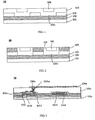
- the array substrate includes: the base substrate 101, the first conductive pattern 102, the insulating layer 103, the second conductive pattern 105 and the protective pattern 106.
- the first conductive pattern 102 is disposed on the base substrate 101; the insulating layer 103 is disposed on the side of the first conductive pattern 102 away from the base substrate 101, and the via hole structure 1031 is in the insulating layer 103; the second conductive pattern 105 is disposed on the side of the insulating layer 103 away from the base substrate 101, and the second conductive pattern 105 is electrically connected with the first conductive pattern 102 at the via hole structure 1031; the protective pattern 106 is disposed on the side of the first conductive pattern 102 away from the base substrate 101, and the orthographic projection of the protective pattern 106 on the base substrate 101 at least partially overlaps the orthographic projection of the via hole structure 1031 on the base substrate 101.
- the protective pattern 106 located on an upper side of the via hole structure 1031 in the example shown in FIG. 1 functions as a protective layer, to protect the first conductive pattern 102 and to avoid undesirable phenomena such as corrosion generated in the first conductive pattern 102 and caused by water vapor entering the first conductive pattern 102 from the environment.
- the second conductive pattern 105 is directly electrically connected with the first conductive pattern 102, which increases a contact area between the second conductive pattern 105 and the first conductive pattern 102, and ensures that the second conductive pattern 105 and the first conductive pattern 102 are well electrically connected with each other.
- the protective pattern 106 is a photoresist pattern, or the protective pattern 106 is a protective pattern formed by using an inorganic material or other organic material.
- the photoresist pattern is formed, for example, by a photoresist used in forming the second conductive pattern 105 by a patterning process, so that the photoresist pattern functioning as the protective pattern and the second conductive pattern 105 are formed in one patterning process without individually forming the protective pattern, thereby saving material and simplifying the manufacturing process.
- the inorganic material is, for example, silicon oxide, silicon nitride or silicon oxynitride or the like
- the organic material is, for example, a resin material or the like, and the embodiments of the present disclosure are not limited thereto.
- the orthographic projection of the protective pattern 106 on the base substrate 101 partially or completely overlap the orthographic projection of the via hole structure 1031 on the base substrate 101.
- the orthographic projection of the protective pattern 106 on the base substrate 101 is located inside the orthographic projection of the via hole structure 1031 on the base substrate 101.
- an upper surface of the protective pattern 106 is coplanar with an upper surface of the second conductive pattern 105, so that the upper surface of the protective pattern 106 and the upper surface of the second conductive pattern 105 form a flat surface.
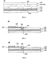
- the array substrate includes: the base substrate 101, the first conductive pattern 102, the insulating layer 103, a connection electrode 104, the second conductive pattern 105 and the protective pattern 106.
- the first conductive pattern 102 is disposed on the base substrate 101; the insulating layer 103 is disposed on the side of the first conductive pattern 102 away from the base substrate 101, and the via hole structure 1031 is in the insulating layer 103; the second conductive pattern 105 is disposed on the side of the insulating layer 103 away from the base substrate 101; the connection electrode 104 is disposed in the via hole structure 1031 of the insulating layer 103, so that the connection electrode 104 electrically connects the second conductive pattern 105 and the first conductive pattern 102; the protective pattern 106 is disposed on a side of the connection electrode 104 away from the base substrate 101, and the orthographic projection of the protective pattern 106 on the base substrate 101 at least partially overlaps the orthographic projection of the via hole structure 1031 on the base substrate 101.
- the protective pattern 106 located on the upper side of the via hole structure 1031 functions as the protective layer, to protect the connection electrode 104 and to avoid undesirable phenomena such as the corrosion generated in the first conductive pattern 102 below the via hole structure 1031 and caused by the water vapor entering the connection electrode 104 from the environment.
- the protective pattern 106 is a photoresist pattern, or the protective pattern 106 is a protective pattern formed by using an inorganic material or other organic material.
- the photoresist pattern is formed, for example, by a photoresist used in forming the connection electrode 104 by a patterning process, so that the photoresist pattern functioning as the protective pattern and the connection electrode are formed in one patterning process without individually forming the protective pattern, thereby saving the material and simplifying the manufacturing process.
- the inorganic material is, for example, silicon oxide, silicon nitride or silicon oxynitride or the like
- the organic material is, for example, a resin material or the like, and the embodiments of the present disclosure are not limited thereto.
- the second conductive pattern 105 and the connection electrode 104 in FIG. 2 are integral with each other (that is, the second conductive pattern 105 and the connection electrode 104 in FIG. 2 are of a one-piece structure), in this case, the second conductive pattern 105 and the connection electrode 104 are formed by patterning the same film with the same patterning process to obtain the same structure as shown in FIG. 2 . In this way, the connection between the second conductive pattern 105 and the connection electrode 104 is more consistent and stable, and the manufacturing process of the array substrate is also simplified.
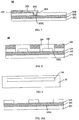
- the array substrate includes a display region 20 and a peripheral region 10, and the first conductive pattern 102, the insulating layer 103, the second conductive pattern 105, the connection electrode 104, and the protective pattern 106 are disposed at least in the peripheral region 10.
- the first conductive pattern 102, the insulating layer 103, the second conductive pattern 105, the connection electrode 104 and the protective pattern 106 are disposed only in the peripheral region 10, or disposed in both the display region 20 and the peripheral region 10.
- the first conductive pattern 102, the insulating layer 103, the second conductive pattern 105, the connection electrode 104 and the protective pattern 106 are disposed only in the display region 20.
- FIG. 2 illustrates a case where the first conductive pattern 102, the insulating layer 103, the connection electrode 104, the second conductive pattern 105 and the protective pattern 106 are disposed in the peripheral region 10.
- the protective pattern 106 disposed on the upper side of the via hole structure 1031 functions as the protective layer to protect the connection electrode 104 and to avoid undesirable phenomena such as the corrosion generated in the first conductive pattern 102 below the via hole structure 1031 and caused by the water vapor entering the connection electrode 104 from the environment.
- the orthographic projection of the protective pattern 106 on the base substrate 101 partially or completely overlaps the orthographic projection of the via hole structure 1031 on the base substrate 101.
- the orthographic projection of the protective pattern 106 on the base substrate 101 is located inside the orthographic projection of the via hole structure 1031 on the base substrate 101.
- the upper surface of the protective pattern 106 is coplanar with an upper surface of the connection electrode 104, so that the upper surface of the protective pattern 106 and the upper surface of the connection electrode 104 form a flat surface.
- the upper surface of the protective pattern 106 is coplanar with the upper surface of the connection electrode 104, that is, the surface which is included by the protective pattern 106 and is away from the base substrate 101 and the surface which is included by the connection electrode 104 and is away from the base substrate 101 are substantially in a same horizontal plane, that is, a shortest distance between the base substrate 101 and the surface which is included by the protective pattern 106 and is away from the base substrate 101 is substantially same as a shortest distance between the base substrate 101 and the surface which is included by the connection electrode 104 and is away from the base substrate 101.
- an orthographic projection of the connection electrode 104 on the base substrate 101 completely coincides with the orthographic projection of the via hole structure 1031 on the base substrate 101; in this case, the orthographic projection of the protective pattern 106 on the base substrate 101 is located inside the orthographic projection of the connection electrode 104 on the base substrate 101.
- the second conductive patterns 105 are disposed on two sides of the via hole structure 1031 and are in direct contact with two side surfaces of the connection electrode 104.
- the upper surface of the second conductive pattern 105, the upper surface of the connection electrode 104 and the upper surface of the protective pattern 106 are all coplanar.
- the upper surface of the second conductive pattern 105, the upper surface of the connection electrode 104 and the upper surface of the protective pattern 106 form a flat surface, and the flat surface is convenient for arrangement of other structures such as a driving circuit or the like in the case that the structures such as the driving circuit or the like are electrically connected with the first conductive pattern 102 through the second conductive pattern 105 and the connection electrode 104.
- the first conductive pattern 102 is, for example, a leading wire electrically connected with a source electrode or a drain electrode or a gate electrode of a thin film transistor or the like in the display region, and the leading wire extends from the display region to the peripheral region, for example, thereby forming the first conductive pattern 102 located in the peripheral region.
- the display region 20 includes the thin film transistor which is disposed, for example, on a base substrate 101a.
- the thin film transistor includes structures such as the gate electrode 1010, the source electrode 1011 and the drain electrode 1012.
- a case where a first leading wire 102a and the source electrode 1011 are disposed in a same layer and electrically connected with each other is shown in FIG. 3 .
- being disposed in the same layer means being formed by patterning a same film with a same patterning process.
- the first leading wire 102a and the source electrode 1011 are integral with each other and are formed by using a same film.
- the first leading wire 102a extends from the display region 20 to the peripheral region 10, thereby forming the first conductive pattern 102 of the peripheral region 10.
- the first leading wire 102a and the gate electrode 101 are disposed in a same layer and electrically connected with each other.
- the first leading wire 102a and the gate electrode 1010 (or the drain electrode 1012) are integral with each other and are formed by using a same film.
- the display region 20 further includes other structures such as a capacitor (for example, the capacitor includes a lower plate 1013 and an upper plate 1014) or the like.
- the capacitor includes a lower plate 1013 and an upper plate 1014) or the like.
- the embodiments of the present disclosure do not limit the specific structure of the display region 20.
- the display region 20 further includes a driving electrode configured for driving a pixel unit in the display region to emit light;
- the driving electrode is, for example, a pixel electrode or a common electrode or the like.
- the driving electrode and the connection electrode are disposed in a same layer.
- the driving electrode located in the display region 20 is a pixel electrode 104a.
- the pixel electrode 104a and the connection electrode 104 which is in the peripheral region 10 are disposed in the same layer; for example, the pixel electrode 104a and the connection electrode 104 which is in the peripheral region 10 are formed by patterning a same film with a same patterning process.
- a material of the driving electrode and the connection electrode 104 is a transparent conductive material.
- the transparent conductive material is indium tin oxide or the like.
- the pixel electrode 104a is electrically connected with the drain electrode 1012 of the thin film transistor, so that the pixel electrode 104a obtains a driving signal transmitted by the thin film transistor and drives the pixel unit in the display region to emit light.
- the drain electrode 1012 of the thin film transistor located in the display region is electrically connected with the pixel electrode 104a through a via hole structure 1031a in an insulating layer 103a, thereby forming a structure of first conductive pattern-insulating layer-second conductive pattern in the display region.
- a protective pattern 106a is further disposed on the pixel electrode 104a, and the orthographic projection of the protective pattern 106a on the base substrate 101a at least partially overlaps the orthographic projection of the via hole structure 1031a in the insulating layer 103a on the base substrate 101a; for example, the orthographic projection of the protective pattern 106a completely overlaps the orthographic projection of the via hole structure 1031a.
- the protective pattern 106a is completely filled in the via hole structure 1031a in the insulating layer 103a.
- the upper surface of the protective pattern 106a and the upper surface of the pixel electrode 104a are substantially in a same plane.
- the protective pattern 106a on the upper side of the via hole structure 1031a in the insulating layer 103a functions as a protective layer to avoid undesirable phenomena such as the corrosion generated in the drain electrode 1012 below the via hole structure 1031a and caused by the water vapor from the environment entering the drain electrode 1012 through the via hole structure 1031a in the insulating layer 103a.
- the protective pattern 106a is formed by a photoresist used in forming the pixel electrode 104a by a patterning process, so that the protective pattern 106a functioning as the protective layer and the pixel electrode 104a are formed by one patterning process without individually forming the protective layer, which saves material and simplifies the manufacturing process.
- the peripheral region 10 further includes a flexible circuit board (chip on FPC (COF)) or an integrated circuit board (IC), and the second conductive pattern 105 is configured to electrically connect the flexible circuit board or the integrated circuit board.
- COF chip on FPC
- IC integrated circuit board
- the integrated circuit board 107 is provided on the second conductive pattern 105, the integrated circuit board 107 is electrically connected with the second conductive pattern 105, and the connection electrode 104 in the via hole structure 1031 of the insulating layer 103 electrically connects the second conductive pattern 105 and the first conductive pattern 102, so that the integrated circuit board 107 provides an electrical signal, such as a data signal or a scan signal or the like, to the thin film transistor in the display region 20.
- the base substrate 101/101a is, for example, a hard substrate such as a glass substrate or a quartz substrate, or a flexible substrate such as polyethylene terephthalate (PET).
- a material of the first conductive pattern 102 is, for example, a metal material which is, for example, an element metal such as aluminum, molybdenum or neodymium, or an alloy material such as an aluminum alloy, a molybdenum alloy or a neodymium alloy.
- the insulating layer 103/103a is, for example, an organic material such as a resin or an inorganic material such as silicon nitride or silicon oxide.
- the second conductive pattern 105 is, for example, a metal material which is, for example, an element metal such as aluminum, molybdenum or neodymium or an alloy material such as an aluminum alloy, a molybdenum alloy or a neodymium alloy, or is a transparent conductive material such as indium tin oxide or the like.
- a material of the photoresist pattern is, for example, a photoresist material such as polyimide (PI), polymethyl methacrylate (PMMA) or organic silicon.
- PI polyimide
- PMMA polymethyl methacrylate
- the embodiments of the present disclosure do not limit the specific materials of the respective functional layers.
- the array substrate includes: the base substrate 101, the first conductive pattern 102, the insulating layer 103, the connection electrode 104, the second conductive pattern 105 and the protective pattern 106.
- the first conductive pattern 102 is disposed on the base substrate 101; the insulating layer 103 is disposed on the side of the first conductive pattern 102 away from the base substrate 101, and the via hole structure 1031 is in the insulating layer 103; the second conductive pattern 105 is disposed on the side of the insulating layer 103 away from the base substrate 101; the connection electrode 104 is disposed in the via hole structure 1031 of the insulating layer 103, two sides of the connection electrode 104 overlaps the insulating layer 103, the orthographic projection of the connection electrode 104 on the base substrate 101 is larger than the orthographic projection of the via hole structure 1031 on the base substrate 101, and the connection electrode 104 electrically connects the second conductive pattern 105 and the first conductive pattern 102; the protective pattern 106 is disposed on the side of the connection electrode 104 away from the base substrate 101, and the orthographic projection of the protective pattern 106 on the base substrate 101 at least partially overlaps the orthographic projection of the via hole structure 1031 on the base substrate 101.
- connection electrode 104 has a groove structure
- the protective pattern 106 is inside the groove structure of the connection electrode 104
- the upper surface of the protective pattern 106 and the upper surface of the connection electrode 104 are substantially coplanar with each other.
- the upper surface of the second conductive pattern 105, the upper surface of the connection electrode 104 and the upper surface of the protective pattern 106 are substantially in the same plane, and the second conductive pattern 105 is formed on one side of the connection electrode 104.
- the second conductive pattern 105 and the connection electrode 104 are integral with each other (that is, the second conductive pattern 105 and the connection electrode 104 are of a one-piece structure), in this case, the second conductive pattern 105 and the connection electrode 104 are formed by patterning the same film with the same patterning process; both of the two sides of the connection electrode 104 overlaps the insulating layer 103, and the orthographic projection of the connection electrode 104 on the base substrate 101 is larger than the orthographic projection of the via hole structure 1031 on the base substrate 101.
- connection electrode 104 For example, only one side of the connection electrode 104 overlaps the insulating layer 103, and the orthogonal projection of the connection electrode 104 on the base substrate 101 is larger than the orthographic projection of the via hole structure 1031 on the base substrate 101.
- the protective pattern 106 is formed on both the second conductive pattern 105 and the connection electrode 104, thereby simultaneously protecting the second conductive pattern 105, the connection electrode 104, and the first conductive pattern 102 which is below the via hole structure 1031.
- the protective pattern 106 is formed on both the second conductive pattern 105 and the connection electrode 104, so as to simultaneously protect the second conductive pattern 105, the connection electrode 104, and the first conductive pattern 102 which is below the via hole structure 1031.
- the integrated circuit board 107 is formed on one side of the peripheral region 10; and by a connection between the second conductive pattern 105 and the connection electrode 104 and a connection between the connection electrode 104 and the first conductive pattern 102, an electrical connection between the integrated circuit board 107 and the first conductive pattern 104 is realized.
- the forming materials, the connection relationships, and the like of the respective functional layers are the same as the above-described respective examples, and details are not described herein again.
- the second conductive pattern 105 is provided on two sides of the via hole structure 1031.
- the protective pattern 106 is provided, for example, in the via hole structure 1031 and provided between the connection electrode 104 and the first conductive pattern 102, as long as it is ensured that the first conductive pattern 102 and a part of the connection electrode 104 are electrically connected with each other.
- the orthographic projection of the connection electrode 104 on the base substrate 101 completely coincides with the orthographic projection of the via hole structure 1031 on the base substrate 101, and in this case, the orthographic projection of the protective pattern 106 on the base substrate 101 is located inside the orthographic projection of the connection electrode 104 on the base substrate 101, so that the protective pattern 106 disposed in the via hole structure 1031 functions as a protective layer, to protect the first conductive pattern 102, to reduce material loss of the first conductive pattern 102 caused by factors such as process fluctuation or etching precision in forming a subsequent film, and to avoid undesirable phenomena such as the corrosion generated in the first conductive pattern 102 below the via hole structure 1031 and caused by the water vapor entering the connection electrode 104 from the environment.
- the solution that the protective pattern 106 is provided in the via hole structure 1031 and provided between the connection electrode 104 and the first conductive pattern 102 is applicable to the example shown in FIG. 5 , and details are not described herein again.
- the embodiments of the present disclosure further provide a display panel.
- the display panel 20 includes the array substrates 100 described in any one of the above embodiments.
- the display panel is, for example, a liquid crystal display panel, an organic light-emitting display panel, or a quantum dot light-emitting display panel, which is not limited thereto.
- the embodiments of the present disclosure further provide a display device which includes the above display panel, and the display device may be any product or component having a display function, such as a mobile phone, a tablet computer, a television, a display, a notebook computer, a digital photo frame, a navigator, and the like.
- a display device which includes the above display panel
- the display device may be any product or component having a display function, such as a mobile phone, a tablet computer, a television, a display, a notebook computer, a digital photo frame, a navigator, and the like.
- the embodiments of the present disclosure further provide a manufacturing method of the array substrate, and the method includes: forming the first conductive pattern on the base substrate; forming an insulating film on the side of the first conductive pattern away from the base substrate, and treating the insulating film to form the insulating layer and the via hole structure in the insulating layer; forming the second conductive pattern on the side of the insulating layer away from the base substrate, so that the second conductive pattern is electrically connected with the first conductive pattern at the via hole structure; and forming the protective pattern on the side of the first conductive pattern away from the base substrate, so that an orthographic projection of the protective pattern on the base substrate at least partially overlaps an orthographic projection of the via hole structure on the base substrate.
- the protective pattern located on the upper side of the via hole structure functions as a protective layer to protect the first conductive pattern and to prevent undesirable phenomena such as the corrosion generated in the first conductive pattern and caused by the water vapor entering the first conductive pattern from the environment.
- the second conductive pattern is directly electrically connected with the first conductive pattern, which increases the contact area between the second conductive pattern and the first conductive pattern, and ensures a better electrical connection between the second conductive pattern and the first conductive pattern.
- the manufacturing method of the array substrate further includes forming the connection electrode, and the connection electrode is formed in the via hole structure to electrically connect the second conductive pattern with the first conductive pattern.
- the protective pattern located on the upper side of the via hole structure functions as a protective layer to protect the connection electrode and prevent undesirable phenomena such as the corrosion generated in the first conductive pattern below the via hole structure and caused by the water vapor entering the connection electrode from the environment.
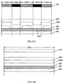
- the second conductive pattern is in direct connection with the first conductive pattern; or the second conductive pattern is in connection with the first conductive pattern through the connection electrode, and the manufacturing process in which the connection electrode and the second conductive pattern are integrally formed is shown in FIG. 10A to FIG. 10F .
- the first conductive pattern 102 is formed on the base substrate 101.
- the base substrate is a hard substrate such as a glass substrate or a quartz substrate, or is a flexible substrate such as polyethylene terephthalate (PET).
- PET polyethylene terephthalate
- the first conductive pattern 102 is formed by, for example, a metal material which is, for example, an element metal such as aluminum, molybdenum or neodymium or an alloy material such as an aluminum alloy, a molybdenum alloy or a neodymium alloy.
- a first conductive material film is firstly formed on the base substrate 101 by sputtering or evaporation, and then a patterning process including procedures such as exposure, development and etching is performed on the first conductive material film to form the first conductive pattern 102.
- the insulating film is formed on the first conductive pattern 102 by deposition or the like, and then the via hole structure 1031 is formed in the insulating film by a patterning process to finally obtain the patterned insulating layer 103.
- the insulating layer 103 is formed by, for example, an organic material such as a resin or an inorganic material such as silicon nitride or silicon oxide, which is not limited in the embodiments of the present disclosure.
- the conductive layer 1040 adopts a metal material which is, for example, an element metal such as aluminum, molybdenum or neodymium, or an alloy material such as an aluminum alloy, a molybdenum alloy or a neodymium alloy; or, for example, the conductive layer 1040 adopts a transparent conductive material such as indium tin oxide or the like.
- the protective layer 1060 adopts, for example, an organic material such as a resin or an inorganic material such as silicon nitride or silicon oxide or the like.
- the first photoresist layer 109 adopts, for example, a photoresist material such as polyimide (PI), polymethyl methacrylate (PMMA) or organic silicon.
- PI polyimide
- PMMA polymethyl methacrylate
- the embodiments of the present disclosure do not limit the specific materials of the respective layers.
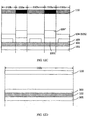
- the first photoresist layer 109 is exposed by using a two-tone mask 110 (for example, the two-tone mask 110a is a halftone mask or a gray tone mask) and is developed to form a first photoresist pattern.
- the first photoresist pattern includes a first photoresist full-retention region, a first photoresist partial-retention region and a first photoresist removal region.
- a region where the first photoresist full-retention region is located is a region where the protective pattern is to be formed
- a region where the first photoresist removal region is located is a region where the protective pattern and the second conductive pattern (or, the protective pattern, the connection electrode and the second conductive pattern) are not formed
- a region where the first photoresist partial-retention region is located is a region except the first photoresist full-retention region and the first photoresist removal region.
- the first photoresist full-retention region corresponds to an opaque region 110a of the two-tone mask 110
- the first photoresist partial-retention region corresponds to a semi-transparent region 110b of the two-tone mask 110
- the first photoresist removal region corresponds to a completely light-transmitting region 110c of the two-tone mask 110.
- the first photoresist removal region corresponds to, for example, a region where the second conductive pattern and the via hole structure in the insulating layer 103 are not formed.
- the photoresist material in the photoresist removal region is firstly removed; then the protective layer and the conductive layer which are in the photoresist removal region are removed by, for example, an etching method, to form the second conductive pattern 105 (or, the second conductive pattern 105 and the connection electrode 104 electrically connected with the second conductive pattern 105, that is, the second conductive pattern 105 and the connection electrode 104 electrically connected with the second conductive pattern 105 are integrally formed by a same film); then, the first photoresist pattern is ashed to retain a portion of the first photoresist layer only in the first photoresist full-retention region; for example, the protective layer outside the first photoresist full-retention region is removed by etching to form the protective pattern; finally, the photoresist in the first photoresist full-retention region is removed by, for example, a lift-off method.
- the protective pattern is thinned by a process such as etching or the like, so that the upper surface of the protective pattern 106 and the upper surface of the second conductive pattern 105 (or, the upper surface of the protective pattern 106, the upper surface of the second conductive pattern 105 and the upper surface of the connection electrode 104) are coplanar with each other.
- one mask is used to pattern the conductive layer 1040 and the protective layer 1060 to form the second conductive pattern 105 (or, the second conductive pattern 105 and the connection electrode 104) and the protective pattern 106, which simplifies the manufacturing process.
- the second conductive pattern 105 and the connection electrode 104 are formed separately, for example.
- the connection electrode 104 electrically connected with the second conductive pattern 105 is formed.
- the protective pattern 106 is formed separately, that is, after the second conductive pattern 105 and the connection electrode 104 are formed, the protective pattern 106 is formed by a patterning process using a single-tone mask.
- the protective pattern 106 is formed of a photoresist.
- the method shown in FIG. 11A to FIG. 11E is employed to manufacture the array substrate.
- the second conductive pattern 105 is formed on the insulating layer 103 by a patterning process.
- a second conductive material layer is formed on the insulating layer 103 by sputtering or evaporation, and then a patterning process is performed on the second conductive material layer to form the patterned second conductive pattern 105.
- the second conductive pattern 105 adopts, for example, a metal material which is, for example, an element metal such as aluminum, molybdenum or neodymium or an alloy material such as an aluminum alloy, a molybdenum alloy or a neodymium alloy, or a transparent conductive material such as indium tin oxide or the like.
- a metal material which is, for example, an element metal such as aluminum, molybdenum or neodymium or an alloy material such as an aluminum alloy, a molybdenum alloy or a neodymium alloy, or a transparent conductive material such as indium tin oxide or the like.
- the conductive layer 1040 and a second photoresist layer 109' are sequentially formed.
- the second photoresist layer 109' is exposed by using a single-tone mask 111 and is developed to form a second photoresist pattern.
- the second photoresist pattern includes a second photoresist retention region and a second photoresist removal region.
- the second photoresist retention region corresponds to an opaque region 111a of the single-tone mask 111, that is, the second photoresist retention region corresponds to a region where the protective pattern 106 is to be formed;
- the second photoresist removal region corresponds to a transparent region 111b of the single-tone mask 111, that is, the second photoresist removal region corresponds to a region outside a region where the protective pattern 106 is to be formed, as shown in FIG. 11A and FIG. 11B .
- the conductive layer 1040 is patterned by using the second photoresist pattern to form the connection electrode 104.
- an ashing process is performed on the second photoresist pattern to form the protective pattern 106, so that a width of the second photoresist pattern is narrowed and a thickness of the second photoresist pattern is reduced.
- the upper surface of the protective pattern 106 is coplanar with both the upper surface of the second conductive pattern 105 and the upper surface of the connection electrode 104.
- the second photoresist pattern is not thinned but is directly used as the protective pattern.
- the protective pattern 106 is formed of the photoresist
- the array substrate is manufactured by the method shown in FIG. 12A to FIG. 12E , and the second conductive pattern 105 and the connection electrode 104 are integrally formed, for example, by a same film.
- the conductive layer 1040 and a third photoresist layer 109" are sequentially formed on the insulating layer 103.
- the third photoresist layer 109" is exposed by using a two-tone mask 110 and is developed to form a third photoresist pattern.
- the third photoresist pattern includes a third photoresist full-retention region, a third photoresist partial-retention region and a third photoresist removal region.
- a region where the third photoresist full-retention region is located is a region where the protective pattern is to be formed
- a region where the third photoresist removal region is located is a region where the protective pattern, the connection electrode and the second conductive pattern are not formed
- a region where the third photoresist partial-retention region is located is a region except the third photoresist full-retention region and the third photoresist removal region.
- the third photoresist full-retention region corresponds to an opaque region 110a of the two-tone mask 110
- the third photoresist partial-retention region corresponds to a semi-transparent region 110b of the two-tone mask 110
- the third photoresist removal region corresponds to a completely light-transmitting region 110c of the two-tone mask 110.
- the photoresist material in the third photoresist removal region is firstly removed, and then the conductive layer in the photoresist removal region is removed by, for example, an etching method to form the second conductive pattern 105 and the connection electrode 104 electrically connected with the second conductive pattern 105 (i.e., the second conductive pattern 105 and the connection electrode 104 electrically connected with the second conductive pattern 105 are integrally formed by the same film).
- the third photoresist pattern is treated, for example, firstly, the photoresist pattern in the third photoresist partial-retention region is removed, and then the photoresist pattern in the third photoresist full-retention region is partially removed to finally form the protective pattern 106 shown in FIG. 12E .
- the photoresist pattern in the third photoresist partial-retention region and the third photoresist full-retention region is removed at the same time by ashing, and finally the protective pattern 106 as shown in FIG. 12E is formed.
- the protective pattern 106 is formed by using the photoresist used in the patterning process for forming the connection electrode, so that the protective pattern 106 serving as the protective layer and the connection electrode 104 are formed in one patterning process without individually forming the protective layer, saving material and simplifying the manufacturing process.
- the array substrate includes the display region 20 and the peripheral region 10; for example, the first conductive pattern 102, the insulating layer 103, the second conductive pattern 105, the connection electrode 104 and the protective pattern 106 are formed at least in the peripheral region 10.
- the first conductive pattern 102, the insulating layer 103, the second conductive pattern 105, the connection electrode 104 and the protective pattern 106 are formed only in the peripheral region 10, or are formed in both the display region 20 and the peripheral region 10.
- the first conductive pattern 102, the insulating layer 103, the second conductive pattern 105, the connection electrode 104 and the protective pattern 106 are formed only in the display region.
- the manufacturing process in which the protective pattern is disposed in the via hole structure and on a side of the second conductive pattern close to the first conductive pattern is as shown in FIG. 13A to FIG. 13D .
- the protective pattern 106 is formed on the insulating layer 103.
- the formation process of the protective pattern is a single-tone mask process, which is not described herein.
- the protective pattern 106 adopts an organic material such as a resin or an inorganic material such as silicon nitride or silicon oxide.
- the conductive layer 1040 and a fourth photoresist layer 109'" are formed on the insulating layer 103 and the protective pattern 106.
- the conductive layer 1040 adopts, for example, a metal material which is, for example, an element metal such as aluminum, molybdenum or neodymium, or an alloy material such as an aluminum alloy, a molybdenum alloy or a neodymium alloy.
- the conductive layer 1040 adopts a transparent conductive material such as indium tin oxide or the like.
- the fourth photoresist layer 109'" adopts, for example, a photoresist material such as polyimide (PI), polymethyl methacrylate (PMMA) or organic silicon.
- PI polyimide
- PMMA polymethyl methacrylate
- organic silicon organic silicon
- the fourth photoresist layer 109'" is exposed by using a single-tone mask and is developed to form a fourth photoresist pattern.
- the fourth photoresist pattern includes a fourth photoresist retention region and a fourth photoresist removal region.
- a region where the fourth photoresist retention region is located is a region where the second conductive pattern (or, the connection electrode and the second conductive pattern) is to be formed
- the fourth photoresist removal region is a region where the second conductive pattern (or, the connection electrode and the second conductive pattern) is not formed.
- the conductive layer of the photoresist removal region is removed by, for example, an etching method to form the second conductive pattern 105 (or, the second conductive pattern 105 and the connection electrode 104 electrically connected with the second conductive pattern 105, that is, the second conductive pattern 105 and the connection electrode 104 electrically connected with the second conductive pattern 105 are integrally formed by the same film).
- the protective pattern 106 is formed in the via hole structure 1031 and formed between the second conductive pattern 105 (or the connection electrode 104) and the first conductive pattern 102, as long as it is ensured that the first conductive pattern 102 and a part of the second conductive pattern 105 (or the connection electrode 104) are electrically connected with each other.
- the orthographic projection of the protective pattern 106 on the base substrate 101 is located inside the orthographic projection of the second conductive pattern 105 (or the connection electrode 104) on the base substrate 101, so that the protective pattern 106 disposed in the via hole structure 1031 functions as a protective layer, to protect the first conductive pattern 102, to reduce the material loss of the first conductive pattern 102 caused by factors such as process fluctuation or etching precision in forming a subsequent film, and to avoid undesirable phenomena such as the corrosion generated in the first conductive pattern 102 below the via hole structure 1031 and caused by the water vapor entering the second conductive pattern 105 from the environment.
- the first conductive pattern 102 is, for example, a leading wire electrically connected with the source electrode, the drain electrode or the gate electrode of the thin film transistor in the display region 20 of the array substrate.
- the source electrode, the drain electrode or the gate electrode or the like located in the display region 20 and the first conductive pattern 102 are formed in a same patterning process.
- the manufacturing method of the array substrate further includes forming the thin film transistor in the display region 20, so that the thin film transistor includes structures such as the gate electrode, the source electrode and the drain electrode; for example, the first conductive pattern 102 and the gate electrode or the source electrode or the drain electrode are integrally formed by the same film.
- the peripheral region 10 further includes, for example, a flexible circuit board or an integrated circuit board, and the second conductive pattern 105 is formed to electrically connect the flexible circuit board or the integrated circuit board, for example.
- the connection electrode 104 disposed in the via hole structure 1031 of the insulating layer 103 electrically connects the second conductive pattern 105 and the first conductive pattern 102, so that the integrated circuit board provides the thin film transistor in the display region with an electrical signal, such as a data signal or a scan signal.
- the manufacturing method of the array substrate is, for example, further includes forming the driving electrode configured for driving the pixel unit in the display region to emit light in the display region 20.
- the driving electrode and the connection electrode 104 are formed by patterning a same film with a same patterning process.
- the driving electrode is the pixel electrode or the common electrode configured for driving the pixel unit in the display region to emit light.
- the material of the driving electrode and the connection electrode 104 is a transparent conductive material, for example, indium tin oxide or the like.
- the driving electrode is the pixel electrode 104a configured for driving the pixel unit in the display region to emit light
- the drain electrode 1012 of the thin film transistor located in the display region is electrically connected with the pixel electrode 104a through the via hole structure 1031a in the insulating layer 103a, thereby forming the structure of first conductive pattern-insulating layer-second conductive pattern in the display region.
- the protective pattern 106a is further disposed on the pixel electrode 104a, and the orthographic projection of the protective pattern 106a on the base substrate 101a at least partially overlaps the orthographic projection of the via hole structure 1031a in the insulating layer 103a on the base substrate 101a; for example, the orthographic projection of the protective pattern 106a completely overlaps the orthographic projection of the via hole structure 1031a.
- the protective pattern 106a on the upper side of the via hole structure functions as a protective layer to avoid undesirable phenomena such as the corrosion generated in the drain electrode 1012 below the via hole structure 1031a and caused by the water vapor entering the pixel electrode 104a from the environment.
- the protective pattern 106a is formed by a photoresist used in forming the pixel electrode 104a by a patterning process, so that the protective pattern 106a functioning as the protective layer and the pixel electrode 104a are formed in one patterning process without individually forming the protective layer, which saves material and simplifies the manufacturing process.
Landscapes
- Physics & Mathematics (AREA)
- Nonlinear Science (AREA)
- Engineering & Computer Science (AREA)
- Microelectronics & Electronic Packaging (AREA)
- Mathematical Physics (AREA)
- Chemical & Material Sciences (AREA)
- Crystallography & Structural Chemistry (AREA)
- General Physics & Mathematics (AREA)
- Optics & Photonics (AREA)
- Devices For Indicating Variable Information By Combining Individual Elements (AREA)
- Electroluminescent Light Sources (AREA)
Abstract
Description
- This application claims the benefit of Chinese patent application No.
201810344260.9 filed on April 17, 2018 - Embodiments of the present disclosure relate to an array substrate, a manufacturing method of the array substrate and a display device.
- At present, an array substrate included in a display panel such as a liquid crystal display panel or an organic light-emitting display panel or the like is formed by a plurality of patterning processes. For example, a thin film transistor having a switching function is formed in a display region of the display panel by the patterning processes, and a leading wire connecting a display region functional element and a peripheral region driving circuit is formed in a peripheral region of the display panel. Adding of one functional layer may cause one patterning process to be added in a manufacturing process, and thus complicate the manufacturing process of the array substrate.
- At least one embodiment of the present disclosure provides an array substrate and the array substrate includes: a base substrate; a first conductive pattern on the base substrate; an insulating layer which is on a side of the first conductive pattern away from the base substrate and is provided with a via hole structure therein; a second conductive pattern which is on a side of the insulating layer away from the base substrate and is electrically connected with the first conductive pattern at the via hole structure; a protective pattern on the side of the first conductive pattern away from the base substrate. An orthographic projection of the protective pattern on the base substrate at least partially overlaps an orthographic projection of the via hole structure on the base substrate.
- For example, in the array substrate provided by at least one embodiment of the present disclosure, the protective pattern is a photoresist pattern.
- For example, in the array substrate provided by at least one embodiment of the present disclosure, an upper surface of the second conductive pattern and an upper surface of the protective pattern are coplanar with each other.
- For example, the array substrate provided by at least one embodiment of the present disclosure further includes the connection electrode, and the connection electrode is in the via hole structure of the insulating layer and is electrically connected with the second conductive pattern and the first conductive pattern.
- For example, in the array substrate provided by at least one embodiment of the present disclosure, the protective pattern is between the connection electrode and the first conductive pattern.
- For example, in the array substrate provided by at least one embodiment of the present disclosure, an upper surface of the protective pattern and an upper surface of the connection electrode are coplanar with each other.
- For example, in the array substrate provided by at least one embodiment of the present disclosure, an upper surface of the second conductive pattern, the upper surface of the connection electrode and the upper surface of the protective pattern are coplanar with each other.
- For example, in the array substrate provided by at least one embodiment of the present disclosure, the second conductive pattern and the connection electrode are integral with each other.
- For example, in the array substrate provided by at least one embodiment of the present disclosure, the array substrate includes a display region and a peripheral region; the first conductive pattern, the insulating layer, the second conductive pattern, the connection electrode and the protective pattern are at least in the peripheral region.
- For example, in the array substrate provided by at least one embodiment of the present disclosure, the peripheral region further includes a flexible circuit board or an integrated circuit board; the second conductive pattern is electrically connected with the flexible circuit board or the integrated circuit board.
- For example, in the array substrate provided by at least one embodiment of the present disclosure, the display region includes a driving electrode configured for driving a pixel unit in the display region to emit light; the driving electrode and the connection electrode are in a same layer.
- At least one embodiment of the present disclosure further provides a manufacturing method of the array substrate, and the manufacturing method includes: providing a base substrate; forming a first conductive pattern on the base substrate; forming an insulating film on a side of the first conductive pattern away from the base substrate, and treating the insulating film to form an insulating layer and a via hole structure in the insulating layer; forming a second conductive pattern on a side of the insulating layer away from the base substrate, so that the second conductive pattern is electrically connected with the first conductive pattern at the via hole structure; and forming a protective pattern on the side of the first conductive pattern away from the base substrate, so that an orthographic projection of the protective pattern on the base substrate at least partially overlaps an orthographic projection of the via hole structure on the base substrate.
- For example, in the manufacturing method of the array substrate according to at least one embodiment of the present disclosure, after the insulating film is treated to form the insulating layer and the via hole structure in the insulating layer, a conductive layer, a protective layer and a first photoresist layer are sequentially formed on the insulating layer; the first photoresist layer is exposed by using a two-tone mask and is developed to form a first photoresist pattern, and the first photoresist pattern includes a first photoresist full-retention region, a first photoresist partial-retention region and a first photoresist removal region; a region where the first photoresist full-retention region is located is a region where the protective pattern is to be formed, a region where the first photoresist removal region is located is a region where the protective pattern and the second conductive pattern are not formed, and a region where the first photoresist partial-retention region is located is a region except the first photoresist full-retention region and the first photoresist removal region; the protective layer and the conductive layer which are in the first photoresist removal region are removed to form the second conductive pattern; the first photoresist pattern is ashed to retain the first photoresist layer only in the first photoresist full-retention region; the protective layer outside the first photoresist full-retention region is removed to form the protective pattern; and the first photoresist layer in the first photoresist full-retention region is removed.
- For example, the manufacturing method of the array substrate provided by at least one embodiment of the present disclosure further includes forming a connection electrode, so that the connection electrode is formed in the via hole structure to electrically connect the second conductive pattern and the first conductive pattern.
- For example, in the manufacturing method of the array substrate according to at least one embodiment of the present disclosure, after the insulating film is treated to form the insulating layer and the via hole structure in the insulating layer, a conductive layer, a protective layer and a first photoresist layer are sequentially formed on the insulating layer; the first photoresist layer is exposed by using a two-tone mask and is developed to form a first photoresist pattern, and the first photoresist pattern includes a first photoresist full-retention region, a first photoresist partial-retention region and a first photoresist removal region; a region where the first photoresist full-retention region is located is a region where the protective pattern is to be formed, a region where the first photoresist removal region is located is a region where the protective pattern, the connection electrode and the second conductive pattern are not formed, and a region where the first photoresist partial-retention region is located is a region except the first photoresist full-retention region and the first photoresist removal region; the protective layer and the conductive layer which are in the first photoresist removal region are removed to form the second conductive pattern and the connection electrode electrically connected with the second conductive pattern; the first photoresist pattern is ashed to retain the first photoresist layer only in the first photoresist full-retention region; the protective layer outside the first photoresist full-retention region is removed to form the protective pattern; and the first photoresist layer in the first photoresist full-retention region is removed.
- For example, in the manufacturing method of the array substrate provided by at least one embodiment of the present disclosure, the protective pattern is formed of a photoresist.
- For example, in the manufacturing method of the array substrate according to at least one embodiment of the present disclosure, after the second conductive pattern is formed, a conductive layer and a second photoresist layer are sequentially formed on the base substrate; the second photoresist layer is exposed by using a single-tone mask and is developed to form a second photoresist pattern, and the conductive layer is patterned by using the second photoresist pattern to form the connection electrode; and the second photoresist pattern is ashed to form the protective pattern.
- For example, in the manufacturing method of the array substrate provided by at least one embodiment of the present disclosure, after the insulating film is treated to form the insulating layer and the via hole structure in the insulating layer, a conductive layer and a third photoresist layer are sequentially formed on the base substrate; the third photoresist layer is exposed by using a two-tone mask and is developed to form a third photoresist pattern, and the third photoresist pattern includes a third photoresist full-retention region, a third photoresist partial-retention region and a third photoresist removal region; a region where the third photoresist full-retention region is located is a region where the protective pattern is to be formed, a region where the third photoresist removal region is located is a region where the protective pattern, the connection electrode and the second conductive pattern are not formed, and a region where the third photoresist partial-retention region is located is a region except the third photoresist full-retention region and the third photoresist removal region; the conductive layer in the third photoresist removal region is removed to form the second conductive pattern and the connection electrode electrically connected with the second conductive pattern; and the third photoresist pattern is ashed to retain the third photoresist layer only in the third photoresist full-retention region to form the protective pattern.
- For example, in the manufacturing method of the array substrate provided by at least one embodiment of the present disclosure, after the insulating film is treated to form the insulating layer and the via hole structure in the insulating layer, the protective pattern is formed in the via hole structure; a conductive layer and a fourth photoresist layer are formed on a side of the protective pattern away from the base substrate; the fourth photoresist layer is exposed by using a single-tone mask and is developed to form a fourth photoresist pattern, and the conductive layer is patterned by using the fourth photoresist pattern to form the second conductive pattern.
- For example, in the manufacturing method of the array substrate according to at least one embodiment of the present disclosure, the array substrate includes a display region and a peripheral region; the first conductive pattern, the insulating layer, the second conductive pattern, the connection electrode and the protective pattern are formed at least in the peripheral region.
- For example, in the manufacturing method of the array substrate according to at least one embodiment of the present disclosure, the peripheral region further includes a flexible circuit board or an integrated circuit board; the second conductive pattern is formed to electrically connect the flexible circuit board or the integrated circuit board.
- For example, in the manufacturing method of the array substrate according to at least one embodiment of the present disclosure, a driving electrode configured for driving a pixel unit in the display region to emit light is formed in the display region; the driving electrode and the connection electrode are formed by using a same film and by a same patterning process.
- For example, in the manufacturing method of the array substrate according to at least one embodiment of the present disclosure, a thin film transistor is formed in the display region, and the thin film transistor includes a gate electrode, a source electrode and a drain electrode; the first conductive pattern is formed by a same film integrally with the gate electrode, the source electrode or the drain electrode.
- At least one embodiment of the present disclosure also provides a display device including the array substrates described in any one of the above embodiments.
- In the array substrate provided by at least one embodiment of the present disclosure, the protective pattern included in the array substrate avoids undesirable phenomena such as corrosion generated in the first conductive pattern located below the via hole structure of the insulating layer.
- In order to clearly illustrate the technical solution of the embodiments of the disclosure, the drawings of the embodiments will be briefly described in the following; it is obvious that the described drawings are only related to some embodiments of the disclosure and thus are not limitative of the disclosure.
-
FIG. 1 is a first schematic view of an array substrate according to the embodiments of the present disclosure; -
FIG. 2 is a second schematic view of the array substrate according to the embodiments of the present disclosure; -
FIG. 3 is a third schematic view of the array substrate according to the embodiments of the present disclosure; -
FIG. 4 is a fourth schematic view of the array substrate according to the embodiments of the present disclosure; -
FIG. 5 is a fifth schematic view of the array substrate according to the embodiments of the present disclosure; -
FIG 6 is a sixth schematic view of the array substrate according to the embodiments of the present disclosure; -
FIG. 7 is a seventh schematic view of the array substrate according to the embodiments of the present disclosure; -
FIG. 8 is an eighth schematic view of the array substrate according to the embodiments of the present disclosure; -
FIG. 9 is a schematic view of a display device according to the embodiments of the present disclosure; -
FIG. 10A-10F are first schematic views of a manufacturing method of the array substrate according to the embodiments of the present disclosure; -
FIG. 11A-11E are second schematic views of the manufacturing method of the array substrate according to the embodiments of the present disclosure; -
FIG. 12A-12E are third schematic views of the manufacturing method of the array substrate according to the embodiments of the present disclosure; -
FIG. 13A-13D are fourth schematic views of the manufacturing method of the array substrate according to the embodiments of the present disclosure. - In order to make objects, technical details and advantages of the embodiments of the disclosure apparent, the technical solutions of the embodiments will be described in a clearly and fully understandable way in connection with the drawings related to the embodiments of the disclosure. Apparently, the described embodiments are just a part but not all of the embodiments of the disclosure. Based on the described embodiments herein, those skilled in the art can obtain other embodiment(s), without any inventive work, which should be within the scope of the disclosure.
- Unless otherwise defined, all the technical and scientific terms used herein have the same meanings as commonly understood by one of ordinary skill in the art to which the present disclosure belongs. The terms "first," "second," etc., which are used in the description and the claims of the present application for disclosure, are not intended to indicate any sequence, amount or importance, but distinguish various components. The terms "comprise," "comprising," "include," "including," etc., are intended to specify that the elements or the objects stated before these terms encompass the elements or the objects and equivalents thereof listed after these terms, but do not preclude the other elements or objects. The phrases "connect", "connected", etc., are not intended to define a physical connection or mechanical connection, but may include an electrical connection, directly or indirectly. "On," "under," "right," "left" and the like are only used to indicate relative position relationship, and when the position of the object which is described is changed, the relative position relationship may be changed accordingly.
- In a manufacturing process of a display panel, leading wires in different layers or conductive layers in different layers are needed to be electrically connected with each other; for example, data lines or scan lines are electrically connected with a driving circuit or the like. For example, an insulating layer is between the leading wires in different layers or the conductive layers in different layers; in this case, for example, a via hole structure is formed in the insulating layer to electrically connect the leading wires in different layers or the conductive layers in different layers. The inventors of the present disclosure found in the study that after forming the via hole structure in the insulating layer and filling a conductive material to electrically connect the leading wires in different layers or the conductive layers in different layers or electrically connect the leading wire and the conductive layer which are located in different layers, loss of a portion of the leading wire or the conductive layer below the via hole structure may be caused due to factors such as process fluctuation or etching precision; at the same time, because of relatively poor denseness of the conductive material covering the via hole structure, a device is easily affected by water vapor in the environment especially if the device is placed in the environment for a long time, resulting in that phenomena such as corrosion of the leading wire or the conductive layer below the via hole structure affect a normal operation of the device.
- At least one embodiment of the present disclosure provides an array substrate, the array substrate includes: a base substrate; a first conductive pattern on the base substrate; an insulating layer which is on a side of the first conductive pattern away from the base substrate and has a via hole structure; a second conductive pattern which is on a side of the insulating layer away from the base substrate and is electrically connected with the first conductive pattern at the via hole structure; and a protective pattern on a side of the first conductive pattern away from the base substrate. An orthographic projection of the protective pattern on the base substrate at least partially overlaps an orthographic projection of the via hole structure on the base substrate.
- At least one embodiment of the present disclosure provides a display device including the above array substrate.
- At least one embodiment of the present disclosure provides a manufacturing method of the array substrate, and the manufacturing method includes: forming a first conductive pattern on a base substrate; forming an insulating film on a side of the first conductive pattern away from the base substrate, and treating the insulating film to form an insulating layer and a via hole structure in the insulating layer; forming a second conductive pattern on a side of the insulating layer away from the base substrate, so' that the second conductive pattern is electrically connected with the first conductive pattern at the via hole structure; and forming a protective pattern on the side of the first conductive pattern away from the base substrate. In the manufacturing method, an orthographic projection of the protective pattern on the base substrate at least partially overlaps an orthographic projection of the via hole structure on the base substrate.
- At least one embodiment of the present disclosure provides the array substrate. In one example of the present disclosure, as shown in
FIG. 1 , the array substrate includes: thebase substrate 101, the firstconductive pattern 102, the insulatinglayer 103, the secondconductive pattern 105 and theprotective pattern 106. The firstconductive pattern 102 is disposed on thebase substrate 101; the insulatinglayer 103 is disposed on the side of the firstconductive pattern 102 away from thebase substrate 101, and the viahole structure 1031 is in the insulatinglayer 103; the secondconductive pattern 105 is disposed on the side of the insulatinglayer 103 away from thebase substrate 101, and the secondconductive pattern 105 is electrically connected with the firstconductive pattern 102 at the viahole structure 1031; theprotective pattern 106 is disposed on the side of the firstconductive pattern 102 away from thebase substrate 101, and the orthographic projection of theprotective pattern 106 on thebase substrate 101 at least partially overlaps the orthographic projection of the viahole structure 1031 on thebase substrate 101. - For example, the
protective pattern 106 located on an upper side of the viahole structure 1031 in the example shown inFIG. 1 functions as a protective layer, to protect the firstconductive pattern 102 and to avoid undesirable phenomena such as corrosion generated in the firstconductive pattern 102 and caused by water vapor entering the firstconductive pattern 102 from the environment. For example, the secondconductive pattern 105 is directly electrically connected with the firstconductive pattern 102, which increases a contact area between the secondconductive pattern 105 and the firstconductive pattern 102, and ensures that the secondconductive pattern 105 and the firstconductive pattern 102 are well electrically connected with each other. - For example, in the example shown in
FIG. 1 , theprotective pattern 106 is a photoresist pattern, or theprotective pattern 106 is a protective pattern formed by using an inorganic material or other organic material. In a situation where theprotective pattern 106 is the photoresist pattern, the photoresist pattern is formed, for example, by a photoresist used in forming the secondconductive pattern 105 by a patterning process, so that the photoresist pattern functioning as the protective pattern and the secondconductive pattern 105 are formed in one patterning process without individually forming the protective pattern, thereby saving material and simplifying the manufacturing process. In a situation where theprotective pattern 106 is formed by using the inorganic material or the organic material, the inorganic material is, for example, silicon oxide, silicon nitride or silicon oxynitride or the like, the organic material is, for example, a resin material or the like, and the embodiments of the present disclosure are not limited thereto. - For example, as shown in
FIG. 1 , the orthographic projection of theprotective pattern 106 on thebase substrate 101 partially or completely overlap the orthographic projection of the viahole structure 1031 on thebase substrate 101. For example, the orthographic projection of theprotective pattern 106 on thebase substrate 101 is located inside the orthographic projection of the viahole structure 1031 on thebase substrate 101. - For example, as shown in
FIG. 1 , an upper surface of theprotective pattern 106 is coplanar with an upper surface of the secondconductive pattern 105, so that the upper surface of theprotective pattern 106 and the upper surface of the secondconductive pattern 105 form a flat surface. - For example, in another embodiment of the present disclosure, as shown in
FIG. 2 , the array substrate includes: thebase substrate 101, the firstconductive pattern 102, the insulatinglayer 103, aconnection electrode 104, the secondconductive pattern 105 and theprotective pattern 106. The firstconductive pattern 102 is disposed on thebase substrate 101; the insulatinglayer 103 is disposed on the side of the firstconductive pattern 102 away from thebase substrate 101, and the viahole structure 1031 is in the insulatinglayer 103; the secondconductive pattern 105 is disposed on the side of the insulatinglayer 103 away from thebase substrate 101; theconnection electrode 104 is disposed in the viahole structure 1031 of the insulatinglayer 103, so that theconnection electrode 104 electrically connects the secondconductive pattern 105 and the firstconductive pattern 102; theprotective pattern 106 is disposed on a side of theconnection electrode 104 away from thebase substrate 101, and the orthographic projection of theprotective pattern 106 on thebase substrate 101 at least partially overlaps the orthographic projection of the viahole structure 1031 on thebase substrate 101. For example, in the example shown inFIG. 2 , theprotective pattern 106 located on the upper side of the viahole structure 1031 functions as the protective layer, to protect theconnection electrode 104 and to avoid undesirable phenomena such as the corrosion generated in the firstconductive pattern 102 below the viahole structure 1031 and caused by the water vapor entering theconnection electrode 104 from the environment. - For example, in the example shown in
FIG. 2 , theprotective pattern 106 is a photoresist pattern, or theprotective pattern 106 is a protective pattern formed by using an inorganic material or other organic material. In a situation where theprotective pattern 106 is the photoresist pattern, the photoresist pattern is formed, for example, by a photoresist used in forming theconnection electrode 104 by a patterning process, so that the photoresist pattern functioning as the protective pattern and the connection electrode are formed in one patterning process without individually forming the protective pattern, thereby saving the material and simplifying the manufacturing process. In a situation where theprotective pattern 106 is formed by using the inorganic material or the organic material, the inorganic material is, for example, silicon oxide, silicon nitride or silicon oxynitride or the like, the organic material is, for example, a resin material or the like, and the embodiments of the present disclosure are not limited thereto. - For example, the second
conductive pattern 105 and theconnection electrode 104 inFIG. 2 are integral with each other (that is, the secondconductive pattern 105 and theconnection electrode 104 inFIG. 2 are of a one-piece structure), in this case, the secondconductive pattern 105 and theconnection electrode 104 are formed by patterning the same film with the same patterning process to obtain the same structure as shown inFIG. 2 . In this way, the connection between the secondconductive pattern 105 and theconnection electrode 104 is more consistent and stable, and the manufacturing process of the array substrate is also simplified. - For example, in at least one embodiment of the present disclosure, as shown in
FIG. 2 and FIG 3 , the array substrate includes adisplay region 20 and aperipheral region 10, and the firstconductive pattern 102, the insulatinglayer 103, the secondconductive pattern 105, theconnection electrode 104, and theprotective pattern 106 are disposed at least in theperipheral region 10. For example, the firstconductive pattern 102, the insulatinglayer 103, the secondconductive pattern 105, theconnection electrode 104 and theprotective pattern 106 are disposed only in theperipheral region 10, or disposed in both thedisplay region 20 and theperipheral region 10. In some examples, the firstconductive pattern 102, the insulatinglayer 103, the secondconductive pattern 105, theconnection electrode 104 and theprotective pattern 106 are disposed only in thedisplay region 20. - For example,
FIG. 2 illustrates a case where the firstconductive pattern 102, the insulatinglayer 103, theconnection electrode 104, the secondconductive pattern 105 and theprotective pattern 106 are disposed in theperipheral region 10. Because theperipheral region 10 originally lacks a protective structure, theprotective pattern 106 disposed on the upper side of the viahole structure 1031 functions as the protective layer to protect theconnection electrode 104 and to avoid undesirable phenomena such as the corrosion generated in the firstconductive pattern 102 below the viahole structure 1031 and caused by the water vapor entering theconnection electrode 104 from the environment. - For example, as shown in
FIG. 2 , the orthographic projection of theprotective pattern 106 on thebase substrate 101 partially or completely overlaps the orthographic projection of the viahole structure 1031 on thebase substrate 101. For example, the orthographic projection of theprotective pattern 106 on thebase substrate 101 is located inside the orthographic projection of the viahole structure 1031 on thebase substrate 101. - For example, as shown in
FIG. 2 , the upper surface of theprotective pattern 106 is coplanar with an upper surface of theconnection electrode 104, so that the upper surface of theprotective pattern 106 and the upper surface of theconnection electrode 104 form a flat surface. - It should be noted that the upper surface of the
protective pattern 106 is coplanar with the upper surface of theconnection electrode 104, that is, the surface which is included by theprotective pattern 106 and is away from thebase substrate 101 and the surface which is included by theconnection electrode 104 and is away from thebase substrate 101 are substantially in a same horizontal plane, that is, a shortest distance between thebase substrate 101 and the surface which is included by theprotective pattern 106 and is away from thebase substrate 101 is substantially same as a shortest distance between thebase substrate 101 and the surface which is included by theconnection electrode 104 and is away from thebase substrate 101. - For example, as shown in
FIG. 2 , an orthographic projection of theconnection electrode 104 on thebase substrate 101 completely coincides with the orthographic projection of the viahole structure 1031 on thebase substrate 101; in this case, the orthographic projection of theprotective pattern 106 on thebase substrate 101 is located inside the orthographic projection of theconnection electrode 104 on thebase substrate 101. - For example, as shown in
FIG. 2 , the secondconductive patterns 105 are disposed on two sides of the viahole structure 1031 and are in direct contact with two side surfaces of theconnection electrode 104. - For example, in the example shown in
FIG. 2 , the upper surface of the secondconductive pattern 105, the upper surface of theconnection electrode 104 and the upper surface of theprotective pattern 106 are all coplanar. In this case, the upper surface of the secondconductive pattern 105, the upper surface of theconnection electrode 104 and the upper surface of theprotective pattern 106 form a flat surface, and the flat surface is convenient for arrangement of other structures such as a driving circuit or the like in the case that the structures such as the driving circuit or the like are electrically connected with the firstconductive pattern 102 through the secondconductive pattern 105 and theconnection electrode 104. - For example, in one example of the present disclosure, the first
conductive pattern 102 is, for example, a leading wire electrically connected with a source electrode or a drain electrode or a gate electrode of a thin film transistor or the like in the display region, and the leading wire extends from the display region to the peripheral region, for example, thereby forming the firstconductive pattern 102 located in the peripheral region. - For example, as shown in
FIG. 3 , thedisplay region 20 includes the thin film transistor which is disposed, for example, on abase substrate 101a. For example, the thin film transistor includes structures such as thegate electrode 1010, thesource electrode 1011 and thedrain electrode 1012. For example, a case where a firstleading wire 102a and thesource electrode 1011 are disposed in a same layer and electrically connected with each other is shown inFIG. 3 . For example; being disposed in the same layer means being formed by patterning a same film with a same patterning process. For example, the firstleading wire 102a and thesource electrode 1011 are integral with each other and are formed by using a same film. For example, the firstleading wire 102a extends from thedisplay region 20 to theperipheral region 10, thereby forming the firstconductive pattern 102 of theperipheral region 10. - For example, in other examples, the first
leading wire 102a and the gate electrode 101 (or the drain electrode 1012) are disposed in a same layer and electrically connected with each other. For example, the firstleading wire 102a and the gate electrode 1010 (or the drain electrode 1012) are integral with each other and are formed by using a same film. - For example, the
display region 20 further includes other structures such as a capacitor (for example, the capacitor includes alower plate 1013 and an upper plate 1014) or the like. The embodiments of the present disclosure do not limit the specific structure of thedisplay region 20. - For example, in an example of the present disclosure, the
display region 20 further includes a driving electrode configured for driving a pixel unit in the display region to emit light; the driving electrode is, for example, a pixel electrode or a common electrode or the like. For example, the driving electrode and the connection electrode are disposed in a same layer. - For example, as shown in
FIG. 3 , the driving electrode located in thedisplay region 20 is apixel electrode 104a. For example, thepixel electrode 104a and theconnection electrode 104 which is in theperipheral region 10 are disposed in the same layer; for example, thepixel electrode 104a and theconnection electrode 104 which is in theperipheral region 10 are formed by patterning a same film with a same patterning process. For example, a material of the driving electrode and theconnection electrode 104 is a transparent conductive material. For example, the transparent conductive material is indium tin oxide or the like. - For example, as shown in
FIG. 3 , thepixel electrode 104a is electrically connected with thedrain electrode 1012 of the thin film transistor, so that thepixel electrode 104a obtains a driving signal transmitted by the thin film transistor and drives the pixel unit in the display region to emit light. - For example, in the example shown in
FIG. 3 , thedrain electrode 1012 of the thin film transistor located in the display region is electrically connected with thepixel electrode 104a through a viahole structure 1031a in an insulatinglayer 103a, thereby forming a structure of first conductive pattern-insulating layer-second conductive pattern in the display region. For example, aprotective pattern 106a is further disposed on thepixel electrode 104a, and the orthographic projection of theprotective pattern 106a on thebase substrate 101a at least partially overlaps the orthographic projection of the viahole structure 1031a in the insulatinglayer 103a on thebase substrate 101a; for example, the orthographic projection of theprotective pattern 106a completely overlaps the orthographic projection of the viahole structure 1031a. Theprotective pattern 106a is completely filled in the viahole structure 1031a in the insulatinglayer 103a. For example, the upper surface of theprotective pattern 106a and the upper surface of thepixel electrode 104a are substantially in a same plane. In this structure, theprotective pattern 106a on the upper side of the viahole structure 1031a in the insulatinglayer 103a functions as a protective layer to avoid undesirable phenomena such as the corrosion generated in thedrain electrode 1012 below the viahole structure 1031a and caused by the water vapor from the environment entering thedrain electrode 1012 through the viahole structure 1031a in the insulatinglayer 103a. - For example, the
protective pattern 106a is formed by a photoresist used in forming thepixel electrode 104a by a patterning process, so that theprotective pattern 106a functioning as the protective layer and thepixel electrode 104a are formed by one patterning process without individually forming the protective layer, which saves material and simplifies the manufacturing process. - For example, in at least one embodiment of the present disclosure, the
peripheral region 10 further includes a flexible circuit board (chip on FPC (COF)) or an integrated circuit board (IC), and the secondconductive pattern 105 is configured to electrically connect the flexible circuit board or the integrated circuit board. - For example, in another example, as shown in
FIG. 4 , theintegrated circuit board 107 is provided on the secondconductive pattern 105, theintegrated circuit board 107 is electrically connected with the secondconductive pattern 105, and theconnection electrode 104 in the viahole structure 1031 of the insulatinglayer 103 electrically connects the secondconductive pattern 105 and the firstconductive pattern 102, so that theintegrated circuit board 107 provides an electrical signal, such as a data signal or a scan signal or the like, to the thin film transistor in thedisplay region 20. - In the above-described example of the present disclosure, the
base substrate 101/101a is, for example, a hard substrate such as a glass substrate or a quartz substrate, or a flexible substrate such as polyethylene terephthalate (PET). A material of the firstconductive pattern 102 is, for example, a metal material which is, for example, an element metal such as aluminum, molybdenum or neodymium, or an alloy material such as an aluminum alloy, a molybdenum alloy or a neodymium alloy. The insulatinglayer 103/103a is, for example, an organic material such as a resin or an inorganic material such as silicon nitride or silicon oxide. The secondconductive pattern 105 is, for example, a metal material which is, for example, an element metal such as aluminum, molybdenum or neodymium or an alloy material such as an aluminum alloy, a molybdenum alloy or a neodymium alloy, or is a transparent conductive material such as indium tin oxide or the like. A material of the photoresist pattern is, for example, a photoresist material such as polyimide (PI), polymethyl methacrylate (PMMA) or organic silicon. The embodiments of the present disclosure do not limit the specific materials of the respective functional layers. - At least one embodiment of the present disclosure further provides another array substrate. As shown in
FIG. 5 , the array substrate includes: thebase substrate 101, the firstconductive pattern 102, the insulatinglayer 103, theconnection electrode 104, the secondconductive pattern 105 and theprotective pattern 106. The firstconductive pattern 102 is disposed on thebase substrate 101; the insulatinglayer 103 is disposed on the side of the firstconductive pattern 102 away from thebase substrate 101, and the viahole structure 1031 is in the insulatinglayer 103; the secondconductive pattern 105 is disposed on the side of the insulatinglayer 103 away from thebase substrate 101; theconnection electrode 104 is disposed in the viahole structure 1031 of the insulatinglayer 103, two sides of theconnection electrode 104 overlaps the insulatinglayer 103, the orthographic projection of theconnection electrode 104 on thebase substrate 101 is larger than the orthographic projection of the viahole structure 1031 on thebase substrate 101, and theconnection electrode 104 electrically connects the secondconductive pattern 105 and the firstconductive pattern 102; theprotective pattern 106 is disposed on the side of theconnection electrode 104 away from thebase substrate 101, and the orthographic projection of theprotective pattern 106 on thebase substrate 101 at least partially overlaps the orthographic projection of the viahole structure 1031 on thebase substrate 101. - For example, as shown in
FIG. 5 , theconnection electrode 104 has a groove structure, and theprotective pattern 106 is inside the groove structure of theconnection electrode 104, and the upper surface of theprotective pattern 106 and the upper surface of theconnection electrode 104 are substantially coplanar with each other. - For example, as shown in
FIG. 5 , the upper surface of the secondconductive pattern 105, the upper surface of theconnection electrode 104 and the upper surface of theprotective pattern 106 are substantially in the same plane, and the secondconductive pattern 105 is formed on one side of theconnection electrode 104. - In another example of the present disclosure, as shown in
FIG. 6 , for example, the secondconductive pattern 105 and theconnection electrode 104 are integral with each other (that is, the secondconductive pattern 105 and theconnection electrode 104 are of a one-piece structure), in this case, the secondconductive pattern 105 and theconnection electrode 104 are formed by patterning the same film with the same patterning process; both of the two sides of theconnection electrode 104 overlaps the insulatinglayer 103, and the orthographic projection of theconnection electrode 104 on thebase substrate 101 is larger than the orthographic projection of the viahole structure 1031 on thebase substrate 101. - For example, only one side of the
connection electrode 104 overlaps the insulatinglayer 103, and the orthogonal projection of theconnection electrode 104 on thebase substrate 101 is larger than the orthographic projection of the viahole structure 1031 on thebase substrate 101. - For example, in another example of the present disclosure, as shown in
FIG. 7 , for example, theprotective pattern 106 is formed on both the secondconductive pattern 105 and theconnection electrode 104, thereby simultaneously protecting the secondconductive pattern 105, theconnection electrode 104, and the firstconductive pattern 102 which is below the viahole structure 1031. - Similarly, for the array substrate shown in
FIG. 7 , for example, theprotective pattern 106 is formed on both the secondconductive pattern 105 and theconnection electrode 104, so as to simultaneously protect the secondconductive pattern 105, theconnection electrode 104, and the firstconductive pattern 102 which is below the viahole structure 1031. - Compared with the foregoing examples, relative positional relationships of some functional layers are changed in the examples of the array substrate shown in
FIG. 5 to FIG. 7 . For example, theintegrated circuit board 107 is formed on one side of theperipheral region 10; and by a connection between the secondconductive pattern 105 and theconnection electrode 104 and a connection between theconnection electrode 104 and the firstconductive pattern 102, an electrical connection between theintegrated circuit board 107 and the firstconductive pattern 104 is realized. In the embodiments of the present disclosure, the forming materials, the connection relationships, and the like of the respective functional layers are the same as the above-described respective examples, and details are not described herein again. - It should be noted that, in the examples of the array substrate shown in
FIG. 5 to FIG. 7 , for example, the secondconductive pattern 105 is provided on two sides of the viahole structure 1031. - In another example of the present disclosure, as shown in
FIG. 8 , theprotective pattern 106 is provided, for example, in the viahole structure 1031 and provided between theconnection electrode 104 and the firstconductive pattern 102, as long as it is ensured that the firstconductive pattern 102 and a part of theconnection electrode 104 are electrically connected with each other. The orthographic projection of theconnection electrode 104 on thebase substrate 101 completely coincides with the orthographic projection of the viahole structure 1031 on thebase substrate 101, and in this case, the orthographic projection of theprotective pattern 106 on thebase substrate 101 is located inside the orthographic projection of theconnection electrode 104 on thebase substrate 101, so that theprotective pattern 106 disposed in the viahole structure 1031 functions as a protective layer, to protect the firstconductive pattern 102, to reduce material loss of the firstconductive pattern 102 caused by factors such as process fluctuation or etching precision in forming a subsequent film, and to avoid undesirable phenomena such as the corrosion generated in the firstconductive pattern 102 below the viahole structure 1031 and caused by the water vapor entering theconnection electrode 104 from the environment. - Likewise, the solution that the
protective pattern 106 is provided in the viahole structure 1031 and provided between theconnection electrode 104 and the firstconductive pattern 102 is applicable to the example shown inFIG. 5 , and details are not described herein again. - The embodiments of the present disclosure further provide a display panel. As shown in
FIG. 9 , thedisplay panel 20 includes thearray substrates 100 described in any one of the above embodiments. The display panel is, for example, a liquid crystal display panel, an organic light-emitting display panel, or a quantum dot light-emitting display panel, which is not limited thereto. - The embodiments of the present disclosure further provide a display device which includes the above display panel, and the display device may be any product or component having a display function, such as a mobile phone, a tablet computer, a television, a display, a notebook computer, a digital photo frame, a navigator, and the like.
- The embodiments of the present disclosure further provide a manufacturing method of the array substrate, and the method includes: forming the first conductive pattern on the base substrate; forming an insulating film on the side of the first conductive pattern away from the base substrate, and treating the insulating film to form the insulating layer and the via hole structure in the insulating layer; forming the second conductive pattern on the side of the insulating layer away from the base substrate, so that the second conductive pattern is electrically connected with the first conductive pattern at the via hole structure; and forming the protective pattern on the side of the first conductive pattern away from the base substrate, so that an orthographic projection of the protective pattern on the base substrate at least partially overlaps an orthographic projection of the via hole structure on the base substrate.
- For example, the protective pattern located on the upper side of the via hole structure functions as a protective layer to protect the first conductive pattern and to prevent undesirable phenomena such as the corrosion generated in the first conductive pattern and caused by the water vapor entering the first conductive pattern from the environment. The second conductive pattern is directly electrically connected with the first conductive pattern, which increases the contact area between the second conductive pattern and the first conductive pattern, and ensures a better electrical connection between the second conductive pattern and the first conductive pattern.
- For example, in still another example of the present disclosure, the manufacturing method of the array substrate further includes forming the connection electrode, and the connection electrode is formed in the via hole structure to electrically connect the second conductive pattern with the first conductive pattern.
- For example, the protective pattern located on the upper side of the via hole structure functions as a protective layer to protect the connection electrode and prevent undesirable phenomena such as the corrosion generated in the first conductive pattern below the via hole structure and caused by the water vapor entering the connection electrode from the environment.
- For example, the second conductive pattern is in direct connection with the first conductive pattern; or the second conductive pattern is in connection with the first conductive pattern through the connection electrode, and the manufacturing process in which the connection electrode and the second conductive pattern are integrally formed is shown in
FIG. 10A to FIG. 10F . - For example, as shown in
FIG. 10A , firstly, the firstconductive pattern 102 is formed on thebase substrate 101. In the embodiments of the present disclosure, for example, the base substrate is a hard substrate such as a glass substrate or a quartz substrate, or is a flexible substrate such as polyethylene terephthalate (PET). The firstconductive pattern 102 is formed by, for example, a metal material which is, for example, an element metal such as aluminum, molybdenum or neodymium or an alloy material such as an aluminum alloy, a molybdenum alloy or a neodymium alloy. - For example, a first conductive material film is firstly formed on the
base substrate 101 by sputtering or evaporation, and then a patterning process including procedures such as exposure, development and etching is performed on the first conductive material film to form the firstconductive pattern 102. - For example, after the first
conductive pattern 102 is formed, for example, the insulating film is formed on the firstconductive pattern 102 by deposition or the like, and then the viahole structure 1031 is formed in the insulating film by a patterning process to finally obtain the patterned insulatinglayer 103. - In the embodiments of the present disclosure, the insulating
layer 103 is formed by, for example, an organic material such as a resin or an inorganic material such as silicon nitride or silicon oxide, which is not limited in the embodiments of the present disclosure. - For example, as shown in
FIG 10B , after the insulatinglayer 103 is formed, aconductive layer 1040, aprotective layer 1060 and afirst photoresist layer 109 are sequentially formed on the insulatinglayer 103. For example, theconductive layer 1040 adopts a metal material which is, for example, an element metal such as aluminum, molybdenum or neodymium, or an alloy material such as an aluminum alloy, a molybdenum alloy or a neodymium alloy; or, for example, theconductive layer 1040 adopts a transparent conductive material such as indium tin oxide or the like. Theprotective layer 1060 adopts, for example, an organic material such as a resin or an inorganic material such as silicon nitride or silicon oxide or the like. Thefirst photoresist layer 109 adopts, for example, a photoresist material such as polyimide (PI), polymethyl methacrylate (PMMA) or organic silicon. The embodiments of the present disclosure do not limit the specific materials of the respective layers. - For example, the
first photoresist layer 109 is exposed by using a two-tone mask 110 (for example, the two-tone mask 110a is a halftone mask or a gray tone mask) and is developed to form a first photoresist pattern. For example, the first photoresist pattern includes a first photoresist full-retention region, a first photoresist partial-retention region and a first photoresist removal region. For example, a region where the first photoresist full-retention region is located is a region where the protective pattern is to be formed, a region where the first photoresist removal region is located is a region where the protective pattern and the second conductive pattern (or, the protective pattern, the connection electrode and the second conductive pattern) are not formed, and a region where the first photoresist partial-retention region is located is a region except the first photoresist full-retention region and the first photoresist removal region. - For example, as shown in
FIG. 10B and FIG. 10C , the first photoresist full-retention region corresponds to anopaque region 110a of the two-tone mask 110, the first photoresist partial-retention region corresponds to asemi-transparent region 110b of the two-tone mask 110, and the first photoresist removal region corresponds to a completely light-transmittingregion 110c of the two-tone mask 110. For example, as shown inFIG. 10C , the first photoresist removal region corresponds to, for example, a region where the second conductive pattern and the via hole structure in the insulatinglayer 103 are not formed. - In the embodiments of the present disclosure, as shown in
FIG. 10D and FIG. 10E , the photoresist material in the photoresist removal region is firstly removed; then the protective layer and the conductive layer which are in the photoresist removal region are removed by, for example, an etching method, to form the second conductive pattern 105 (or, the secondconductive pattern 105 and theconnection electrode 104 electrically connected with the secondconductive pattern 105, that is, the secondconductive pattern 105 and theconnection electrode 104 electrically connected with the secondconductive pattern 105 are integrally formed by a same film); then, the first photoresist pattern is ashed to retain a portion of the first photoresist layer only in the first photoresist full-retention region; for example, the protective layer outside the first photoresist full-retention region is removed by etching to form the protective pattern; finally, the photoresist in the first photoresist full-retention region is removed by, for example, a lift-off method. For example, as shown inFIG. 10F , after the photoresist in the first photoresist full-retention region is lifted off, the protective pattern is thinned by a process such as etching or the like, so that the upper surface of theprotective pattern 106 and the upper surface of the second conductive pattern 105 (or, the upper surface of theprotective pattern 106, the upper surface of the secondconductive pattern 105 and the upper surface of the connection electrode 104) are coplanar with each other. - As shown in
FIG. 10B to FIG. 10F , for example, one mask is used to pattern theconductive layer 1040 and theprotective layer 1060 to form the second conductive pattern 105 (or, the secondconductive pattern 105 and the connection electrode 104) and theprotective pattern 106, which simplifies the manufacturing process. - In the embodiments of the present disclosure, the second
conductive pattern 105 and theconnection electrode 104 are formed separately, for example. For example, after the secondconductive pattern 105 is formed by a patterning process, theconnection electrode 104 electrically connected with the secondconductive pattern 105 is formed. For example, in the embodiments of the present disclosure, theprotective pattern 106 is formed separately, that is, after the secondconductive pattern 105 and theconnection electrode 104 are formed, theprotective pattern 106 is formed by a patterning process using a single-tone mask. - For example, in one example of the present disclosure, the
protective pattern 106 is formed of a photoresist. - For example, in a case where the
protective pattern 106 is formed of the photoresist, for example, the method shown inFIG. 11A to FIG. 11E is employed to manufacture the array substrate. For example, as shown inFIG. 11A andFIG. 11B , after the insulatinglayer 103 is formed, the secondconductive pattern 105 is formed on the insulatinglayer 103 by a patterning process. For example, a second conductive material layer is formed on the insulatinglayer 103 by sputtering or evaporation, and then a patterning process is performed on the second conductive material layer to form the patterned secondconductive pattern 105. The secondconductive pattern 105 adopts, for example, a metal material which is, for example, an element metal such as aluminum, molybdenum or neodymium or an alloy material such as an aluminum alloy, a molybdenum alloy or a neodymium alloy, or a transparent conductive material such as indium tin oxide or the like. - For example, after the second
conductive pattern 105 is formed, theconductive layer 1040 and a second photoresist layer 109' are sequentially formed. For example, the second photoresist layer 109' is exposed by using a single-tone mask 111 and is developed to form a second photoresist pattern. For example, the second photoresist pattern includes a second photoresist retention region and a second photoresist removal region. For example, the second photoresist retention region corresponds to anopaque region 111a of the single-tone mask 111, that is, the second photoresist retention region corresponds to a region where theprotective pattern 106 is to be formed; the second photoresist removal region corresponds to atransparent region 111b of the single-tone mask 111, that is, the second photoresist removal region corresponds to a region outside a region where theprotective pattern 106 is to be formed, as shown inFIG. 11A andFIG. 11B . - For example, as shown in
FIG 11C andFIG 11D , theconductive layer 1040 is patterned by using the second photoresist pattern to form theconnection electrode 104. As shown inFIG. 11E , for example, an ashing process is performed on the second photoresist pattern to form theprotective pattern 106, so that a width of the second photoresist pattern is narrowed and a thickness of the second photoresist pattern is reduced. In this case, the upper surface of theprotective pattern 106 is coplanar with both the upper surface of the secondconductive pattern 105 and the upper surface of theconnection electrode 104. Or, for example, the second photoresist pattern is not thinned but is directly used as the protective pattern. - For example, in the case where the
protective pattern 106 is formed of the photoresist, for example, the array substrate is manufactured by the method shown inFIG. 12A to FIG. 12E , and the secondconductive pattern 105 and theconnection electrode 104 are integrally formed, for example, by a same film. - For example, as shown in
FIG 12A and FIG 12B , after the viahole structure 1031 in the insulatinglayer 103 is formed, theconductive layer 1040 and athird photoresist layer 109" are sequentially formed on the insulatinglayer 103. Thethird photoresist layer 109" is exposed by using a two-tone mask 110 and is developed to form a third photoresist pattern. For example, the third photoresist pattern includes a third photoresist full-retention region, a third photoresist partial-retention region and a third photoresist removal region. For example, a region where the third photoresist full-retention region is located is a region where the protective pattern is to be formed, a region where the third photoresist removal region is located is a region where the protective pattern, the connection electrode and the second conductive pattern are not formed, and a region where the third photoresist partial-retention region is located is a region except the third photoresist full-retention region and the third photoresist removal region. - For example, the third photoresist full-retention region corresponds to an
opaque region 110a of the two-tone mask 110, the third photoresist partial-retention region corresponds to asemi-transparent region 110b of the two-tone mask 110, and the third photoresist removal region corresponds to a completely light-transmittingregion 110c of the two-tone mask 110. - For example, as shown in
FIG 12C and FIG. 12D , the photoresist material in the third photoresist removal region is firstly removed, and then the conductive layer in the photoresist removal region is removed by, for example, an etching method to form the secondconductive pattern 105 and theconnection electrode 104 electrically connected with the second conductive pattern 105 (i.e., the secondconductive pattern 105 and theconnection electrode 104 electrically connected with the secondconductive pattern 105 are integrally formed by the same film). Then, the third photoresist pattern is treated, for example, firstly, the photoresist pattern in the third photoresist partial-retention region is removed, and then the photoresist pattern in the third photoresist full-retention region is partially removed to finally form theprotective pattern 106 shown inFIG. 12E . For example, in other examples, for example, the photoresist pattern in the third photoresist partial-retention region and the third photoresist full-retention region is removed at the same time by ashing, and finally theprotective pattern 106 as shown inFIG. 12E is formed. - In the method shown in
FIG. 11A to FIG. 11E and the method shown inFIG. 12A to FIG. 12E , theprotective pattern 106 is formed by using the photoresist used in the patterning process for forming the connection electrode, so that theprotective pattern 106 serving as the protective layer and theconnection electrode 104 are formed in one patterning process without individually forming the protective layer, saving material and simplifying the manufacturing process. - For example, in at least one embodiment of the present disclosure, the array substrate includes the
display region 20 and theperipheral region 10; for example, the firstconductive pattern 102, the insulatinglayer 103, the secondconductive pattern 105, theconnection electrode 104 and theprotective pattern 106 are formed at least in theperipheral region 10. For example, the firstconductive pattern 102, the insulatinglayer 103, the secondconductive pattern 105, theconnection electrode 104 and theprotective pattern 106 are formed only in theperipheral region 10, or are formed in both thedisplay region 20 and theperipheral region 10. In some examples, the firstconductive pattern 102, the insulatinglayer 103, the secondconductive pattern 105, theconnection electrode 104 and theprotective pattern 106 are formed only in the display region. - For example, in a situation where the second conductive pattern is in direct connection with the first conductive pattern (or, the second conductive pattern is in connection with the first conductive pattern through the connection electrode, and the connection electrode and the second conductive pattern are integral with each other), the manufacturing process in which the protective pattern is disposed in the via hole structure and on a side of the second conductive pattern close to the first conductive pattern (or, the protective pattern is disposed in the via hole structure and on a side of the connection electrode close to the first conductive pattern) is as shown in
FIG. 13A to FIG. 13D . - For example, as shown in
FIG. 13A , after the insulatinglayer 103 is formed, theprotective pattern 106 is formed on the insulatinglayer 103. For example, the formation process of the protective pattern is a single-tone mask process, which is not described herein. For example, theprotective pattern 106 adopts an organic material such as a resin or an inorganic material such as silicon nitride or silicon oxide. - For example, as shown in
FIG. 13B , theconductive layer 1040 and a fourth photoresist layer 109'" are formed on the insulatinglayer 103 and theprotective pattern 106. Theconductive layer 1040 adopts, for example, a metal material which is, for example, an element metal such as aluminum, molybdenum or neodymium, or an alloy material such as an aluminum alloy, a molybdenum alloy or a neodymium alloy. For example, theconductive layer 1040 adopts a transparent conductive material such as indium tin oxide or the like. The fourth photoresist layer 109'" adopts, for example, a photoresist material such as polyimide (PI), polymethyl methacrylate (PMMA) or organic silicon. The embodiments of the present disclosure do not limit the specific materials of the respective layers. - For example, as shown in
FIG. 13C , the fourth photoresist layer 109'" is exposed by using a single-tone mask and is developed to form a fourth photoresist pattern. For example, the fourth photoresist pattern includes a fourth photoresist retention region and a fourth photoresist removal region. For example, a region where the fourth photoresist retention region is located is a region where the second conductive pattern (or, the connection electrode and the second conductive pattern) is to be formed, and the fourth photoresist removal region is a region where the second conductive pattern (or, the connection electrode and the second conductive pattern) is not formed. - For example, as shown in
FIG. 13D , the conductive layer of the photoresist removal region is removed by, for example, an etching method to form the second conductive pattern 105 (or, the secondconductive pattern 105 and theconnection electrode 104 electrically connected with the secondconductive pattern 105, that is, the secondconductive pattern 105 and theconnection electrode 104 electrically connected with the secondconductive pattern 105 are integrally formed by the same film). - For example, the
protective pattern 106 is formed in the viahole structure 1031 and formed between the second conductive pattern 105 (or the connection electrode 104) and the firstconductive pattern 102, as long as it is ensured that the firstconductive pattern 102 and a part of the second conductive pattern 105 (or the connection electrode 104) are electrically connected with each other. The orthographic projection of theprotective pattern 106 on thebase substrate 101 is located inside the orthographic projection of the second conductive pattern 105 (or the connection electrode 104) on thebase substrate 101, so that theprotective pattern 106 disposed in the viahole structure 1031 functions as a protective layer, to protect the firstconductive pattern 102, to reduce the material loss of the firstconductive pattern 102 caused by factors such as process fluctuation or etching precision in forming a subsequent film, and to avoid undesirable phenomena such as the corrosion generated in the firstconductive pattern 102 below the viahole structure 1031 and caused by the water vapor entering the secondconductive pattern 105 from the environment. - In at least one embodiment of the present disclosure, the first
conductive pattern 102 is, for example, a leading wire electrically connected with the source electrode, the drain electrode or the gate electrode of the thin film transistor in thedisplay region 20 of the array substrate. For example, the source electrode, the drain electrode or the gate electrode or the like located in thedisplay region 20 and the firstconductive pattern 102 are formed in a same patterning process. - For example, the manufacturing method of the array substrate further includes forming the thin film transistor in the
display region 20, so that the thin film transistor includes structures such as the gate electrode, the source electrode and the drain electrode; for example, the firstconductive pattern 102 and the gate electrode or the source electrode or the drain electrode are integrally formed by the same film. - In at least one embodiment of the present disclosure, the
peripheral region 10 further includes, for example, a flexible circuit board or an integrated circuit board, and the secondconductive pattern 105 is formed to electrically connect the flexible circuit board or the integrated circuit board, for example. In at least one embodiment of the present disclosure, theconnection electrode 104 disposed in the viahole structure 1031 of the insulatinglayer 103 electrically connects the secondconductive pattern 105 and the firstconductive pattern 102, so that the integrated circuit board provides the thin film transistor in the display region with an electrical signal, such as a data signal or a scan signal. - In at least one embodiment of the present disclosure, the manufacturing method of the array substrate is, for example, further includes forming the driving electrode configured for driving the pixel unit in the display region to emit light in the
display region 20. For example, the driving electrode and theconnection electrode 104 are formed by patterning a same film with a same patterning process. For example, the driving electrode is the pixel electrode or the common electrode configured for driving the pixel unit in the display region to emit light. For example, the material of the driving electrode and theconnection electrode 104 is a transparent conductive material, for example, indium tin oxide or the like. - Referring to
FIG. 3 , in the example shown inFIG. 3 , the driving electrode is thepixel electrode 104a configured for driving the pixel unit in the display region to emit light, and in this case, thedrain electrode 1012 of the thin film transistor located in the display region is electrically connected with thepixel electrode 104a through the viahole structure 1031a in the insulatinglayer 103a, thereby forming the structure of first conductive pattern-insulating layer-second conductive pattern in the display region. For example, theprotective pattern 106a is further disposed on thepixel electrode 104a, and the orthographic projection of theprotective pattern 106a on thebase substrate 101a at least partially overlaps the orthographic projection of the viahole structure 1031a in the insulatinglayer 103a on thebase substrate 101a; for example, the orthographic projection of theprotective pattern 106a completely overlaps the orthographic projection of the viahole structure 1031a. In this structure, theprotective pattern 106a on the upper side of the via hole structure functions as a protective layer to avoid undesirable phenomena such as the corrosion generated in thedrain electrode 1012 below the viahole structure 1031a and caused by the water vapor entering thepixel electrode 104a from the environment. - For example, the
protective pattern 106a is formed by a photoresist used in forming thepixel electrode 104a by a patterning process, so that theprotective pattern 106a functioning as the protective layer and thepixel electrode 104a are formed in one patterning process without individually forming the protective layer, which saves material and simplifies the manufacturing process. - There are also the following points to be explained:
- (1) The drawings of the embodiments of the present disclosure only relate to the structures mentioned in the embodiments of the present disclosure, and other structures can be referred to the general design.
- (2) For the sake of clarity, in the drawings for describing the embodiments of the present disclosure, the thicknesses of layers or regions are enlarged or reduced, that is, the drawings are not drawn to actual scales. It will be understood that when an element such as a layer, a film, a region or a substrate is referred to as being "on" or "below" another element, the element may be "directly" "on" or "below" the another element or there may be an intermediate element between the element and the another element.
- (3) In the case of no conflict, the embodiments of the present disclosure and the features in the embodiments may be combined with each other to obtain a new embodiment.
- What are described above are only the specific embodiments of the present disclosure, but the protection scope of the present disclosure is not limited thereto, any person skilled in the art can easily think of changes or substitutions within the technical scope of the disclosure, and these changes or substitutions should be within the protection scope of the present disclosure. Therefore, the protection scope of the disclosure should be determined by the scope of the claims.
Claims (20)
- An array substrate, comprising:a base substrate;a first conductive pattern on the base substrate;an insulating layer on a side of the first conductive pattern away from the base substrate, wherein a via hole structure is in the insulating layer;a second conductive pattern on a side of the insulating layer away from the base substrate, wherein the second conductive pattern is electrically connected with the first conductive pattern at the via hole structure;a protective pattern on the side of the first conductive pattern away from the base substrate;wherein an orthographic projection of the protective pattern on the base substrate at least partially overlaps an orthographic projection of the via hole structure on the base substrate.
- The array substrate according to claim 1, wherein the protective pattern is a photoresist pattern.
- The array substrate according to claim 1 or 2, wherein an upper surface of the second conductive pattern and an upper surface of the protective pattern are coplanar with each other.
- The array substrate according to any one of claims 1 to 3, further comprising a connection electrode, wherein the connection electrode is in the via hole structure of the insulating layer and is electrically connected with the second conductive pattern and the first conductive pattern.
- The array substrate according to claim 4, wherein the protective pattern is between the connection electrode and the first conductive pattern.
- The array substrate according to claim 4, wherein an upper surface of the protective pattern and an upper surface of the connection electrode are coplanar with each other.
- The array substrate according to claim. 6, wherein an upper surface of the second conductive pattern, the upper surface of the connection electrode and the upper surface of the protective pattern are coplanar with each other.
- The array substrate according to any one of claims 4 to 7, wherein the second conductive pattern and the connection electrode are integral with each other.
- The array substrate according to any one of claims 4-7, comprising a display region and a peripheral region, wherein the first conductive pattern, the insulating layer, the second conductive pattern, the connection electrode and the protective pattern are at least in the peripheral region.
- The array substrate according to claim 9, wherein
the peripheral region further comprises a flexible circuit board or an integrated circuit board;
the second conductive pattern is electrically connected with the flexible circuit board or the integrated circuit board. - The array substrate according to claim 9, wherein
the display region comprises a driving electrode configured for driving a pixel unit in the display region to emit light;
the driving electrode and the connection electrode are in a same layer. - A manufacturing method of an array substrate, comprising:providing a base substrate;forming a first conductive pattern on the base substrate;forming an insulating film on a side of the first conductive pattern away from the base substrate, and treating the insulating film to form an insulating layer and a via hole structure in the insulating layer;forming a second conductive pattern on a side of the insulating layer away from the base substrate, wherein the second conductive pattern is electrically connected with the first conductive pattern at the via hole structure; andforming a protective pattern on the side of the first conductive pattern away from the base substrate;wherein an orthographic projection of the protective pattern on the base substrate at least partially overlaps an orthographic projection of the via hole structure on the base substrate.
- The manufacturing method of the array substrate according to claim 12, wherein after the insulating film is treated to form the insulating layer and the via hole structure in the insulating layer, a conductive layer, a protective layer and a first photoresist layer are sequentially formed on the insulating layer;
the first photoresist layer is exposed by using a two-tone mask and is developed to form a first photoresist pattern, the first photoresist pattern comprises a first photoresist full-retention region, a first photoresist partial-retention region and a first photoresist removal region, a region where the first photoresist full-retention region is located is a region where the protective pattern is to be formed, a region where the first photoresist removal region is located is a region where the protective pattern and the second conductive pattern are not formed, and a region where the first photoresist partial-retention region is located is a region except the first photoresist full-retention region and the first photoresist removal region;
the protective layer and the conductive layer which are in the first photoresist removal region are removed to form the second conductive pattern;
the first photoresist pattern is ashed to retain the first photoresist layer only in the first photoresist full-retention region;
the protective layer outside the first photoresist full-retention region is removed to form the protective pattern; and
the first photoresist layer in the first photoresist full-retention region is removed. - The manufacturing method of the array substrate according to claim 12, further comprising forming a connection electrode, wherein the connection electrode is formed in the via hole structure to electrically connect the second conductive pattern and the first conductive pattern.
- The manufacturing method of the array substrate according to claim 14, wherein after the insulating film is treated to form the insulating layer and the via hole structure in the insulating layer, a conductive layer, a protective layer and a first photoresist layer are sequentially formed on the insulating layer;
the first photoresist layer is exposed by using a two-tone mask and is developed to form a first photoresist pattern, the first photoresist pattern comprises a first photoresist full-retention region, a first photoresist partial-retention region and a first photoresist removal region, a region where the first photoresist full-retention region is located is a region where the protective pattern is to be formed, a region where the first photoresist removal region is located is a region where the protective pattern, the connection electrode and the second conductive pattern are not formed, and a region where the first photoresist partial-retention region is located is a region except the first photoresist full-retention region and the first photoresist removal region;
the protective layer and the conductive layer which are in the first photoresist removal region are removed to form the second conductive pattern and the connection electrode electrically connected with the second conductive pattern;
the first photoresist pattern is ashed to retain the first photoresist layer only in the first photoresist full-retention region;
the protective layer outside the first photoresist full-retention region is removed to form the protective pattern; and
the first photoresist layer in the first photoresist full-retention region is removed. - The manufacturing method of the array substrate according to claim 14, wherein the protective pattern is formed of a photoresist.
- The manufacturing method of the array substrate according to claim 16, wherein
after the second conductive pattern is formed on the side of the insulating layer away from the base substrate, a conductive layer and a second photoresist layer are sequentially formed on the base substrate;
the second photoresist layer is exposed by using a single-tone mask and is developed to form a second photoresist pattern, and the conductive layer is patterned by using the second photoresist pattern to form the connection electrode; and
the second photoresist pattern is ashed to form the protective pattern. - The manufacturing method of the array substrate according to claim 16, wherein after the insulating film is treated to form the insulating layer and the via hole structure in the insulating layer, a conductive layer and a third photoresist layer are sequentially formed on the base substrate;
the third photoresist layer is exposed by using a two-tone mask and is developed to form a third photoresist pattern, the third photoresist pattern comprises a third photoresist full-retention region, a third photoresist partial-retention region and a third photoresist removal region, a region where the third photoresist full-retention region is located is a region where the protective pattern is to be formed, a region where the third photoresist removal region is located is a region where the protective pattern, the connection electrode and the second conductive pattern are not formed, and a region where the third photoresist partial-retention region is located is a region except the third photoresist full-retention region and the third photoresist removal region;
the conductive layer in the third photoresist removal region is removed to form the second conductive pattern and the connection electrode electrically connected with the second conductive pattern; and
the third photoresist pattern is ashed to retain the third photoresist layer only in the third photoresist full-retention region to form the protective pattern. - The manufacturing method of the array substrate according to claim 12, wherein after the insulating film is treated to form the insulating layer and the via hole structure in the insulating layer, the protective pattern is formed in the via hole structure; and a conductive layer and a fourth photoresist layer are formed on a side of the protective pattern away from the base substrate;
the fourth photoresist layer is exposed by using a single-tone mask and is developed to form a fourth photoresist pattern, and the conductive layer is patterned by using the fourth photoresist pattern to form the second conductive pattern. - A display device, comprising the array substrate according to any one of claims 1-11.
Applications Claiming Priority (2)
| Application Number | Priority Date | Filing Date | Title |
|---|---|---|---|
| CN201810344260.9A CN110061058A (en) | 2018-04-17 | 2018-04-17 | Array substrate and preparation method thereof, display device |
| PCT/CN2018/116771 WO2019200912A1 (en) | 2018-04-17 | 2018-11-21 | Array substrate and preparation method therefor, and display device |
Publications (2)
| Publication Number | Publication Date |
|---|---|
| EP3787021A1 true EP3787021A1 (en) | 2021-03-03 |
| EP3787021A4 EP3787021A4 (en) | 2022-02-23 |
Family
ID=67315507
Family Applications (1)
| Application Number | Title | Priority Date | Filing Date |
|---|---|---|---|
| EP18899004.8A Withdrawn EP3787021A4 (en) | 2018-04-17 | 2018-11-21 | MATRIX SUBSTRATE AND METHOD FOR PREPARING IT, AND DISPLAY DEVICE |
Country Status (4)
| Country | Link |
|---|---|
| US (1) | US20210358973A1 (en) |
| EP (1) | EP3787021A4 (en) |
| CN (1) | CN110061058A (en) |
| WO (1) | WO2019200912A1 (en) |
Families Citing this family (5)
| Publication number | Priority date | Publication date | Assignee | Title |
|---|---|---|---|---|
| CN113270460B (en) * | 2021-05-18 | 2025-02-11 | 京东方科技集团股份有限公司 | Display panel and manufacturing method thereof, and display device |
| CN113471219A (en) * | 2021-06-30 | 2021-10-01 | 云谷(固安)科技有限公司 | Metal wiring of semiconductor device and preparation method thereof |
| CN113571535B (en) * | 2021-07-23 | 2024-02-20 | 京东方科技集团股份有限公司 | Array substrate, manufacturing method of array substrate and display panel |
| CN113707673B (en) * | 2021-08-27 | 2023-12-26 | 成都京东方光电科技有限公司 | A display substrate and its preparation method and display device |
| CN114023770B (en) * | 2021-10-28 | 2025-08-26 | 合肥京东方瑞晟科技有限公司 | Array substrate and preparation method thereof, and light-emitting device |
Family Cites Families (22)
| Publication number | Priority date | Publication date | Assignee | Title |
|---|---|---|---|---|
| KR101039022B1 (en) * | 2004-02-11 | 2011-06-03 | 삼성전자주식회사 | Contact portion and manufacturing method thereof, thin film transistor array panel and manufacturing method thereof |
| KR20100021847A (en) * | 2008-08-18 | 2010-02-26 | 삼성전자주식회사 | Thin film transistor array panel and method for manufacturing the same |
| CN102171746B (en) * | 2008-10-02 | 2015-05-20 | 夏普株式会社 | Display device substrate, display device substrate manufacturing method, display device, liquid crystal display (LCD) device, LCD manufacturing method, and organic electroluminescence display device |
| CN101726875A (en) * | 2008-10-10 | 2010-06-09 | 华映视讯(吴江)有限公司 | Bonding pad structure, active component array substrate and liquid crystal display panel |
| TWI441122B (en) * | 2011-12-30 | 2014-06-11 | 友達光電股份有限公司 | Array substrate structure of display panel and manufacturing method thereof |
| KR102011274B1 (en) * | 2012-12-10 | 2019-08-19 | 삼성디스플레이 주식회사 | Method of manufacturing display substrate |
| KR102132445B1 (en) * | 2013-12-31 | 2020-07-09 | 엘지디스플레이 주식회사 | Liquid Crystal Display Panel And Manufacturing Method Of The Same |
| TWI553534B (en) * | 2014-10-09 | 2016-10-11 | 友達光電股份有限公司 | Capacitive touch panel, method of fabricating capacitive touch panel and touch display device |
| CN104576655B (en) * | 2014-12-01 | 2017-07-18 | 深圳市华星光电技术有限公司 | A kind of COA substrates and preparation method thereof |
| CN104460154A (en) * | 2014-12-15 | 2015-03-25 | 京东方科技集团股份有限公司 | Array substrate and manufacturing method thereof and display device |
| CN104460070B (en) * | 2014-12-31 | 2018-09-07 | 合肥鑫晟光电科技有限公司 | Display panel and preparation method thereof, display device |
| CN105185786B (en) * | 2015-07-24 | 2018-11-27 | 深圳市华星光电技术有限公司 | A kind of array substrate and its manufacturing method |
| CN105372889A (en) * | 2015-10-23 | 2016-03-02 | 深圳市华星光电技术有限公司 | Display device, COA baseplate and manufacture method for same |
| CN105304649B (en) * | 2015-10-28 | 2019-01-18 | 京东方科技集团股份有限公司 | Array substrate and preparation method thereof, display panel, display device |
| CN105702685B (en) * | 2016-03-01 | 2018-09-04 | 京东方科技集团股份有限公司 | A kind of array substrate and preparation method thereof, display device |
| CN105845692A (en) * | 2016-03-25 | 2016-08-10 | 京东方科技集团股份有限公司 | Display substrate, display apparatus and manufacture method of display substrate |
| CN105629614A (en) * | 2016-03-29 | 2016-06-01 | 京东方科技集团股份有限公司 | Array substrate and manufacturing method thereof, display panel and display device |
| CN106057824A (en) * | 2016-08-03 | 2016-10-26 | 京东方科技集团股份有限公司 | Array substrate, manufacturing method thereof and display device |
| CN106646969A (en) * | 2016-11-22 | 2017-05-10 | 深圳市华星光电技术有限公司 | COA type liquid crystal panel and manufacturing method thereof |
| CN106783747A (en) * | 2017-01-03 | 2017-05-31 | 京东方科技集团股份有限公司 | A kind of preparation method of array base palte, array base palte and display device |
| US10269834B2 (en) * | 2017-01-10 | 2019-04-23 | A.U. Vista, Inc. | TFT array for use in a high-resolution display panel and method for making same |
| CN107065317A (en) * | 2017-05-19 | 2017-08-18 | 深圳市华星光电技术有限公司 | Liquid crystal display panel and its manufacture method and curved-surface display equipment |
-
2018
- 2018-04-17 CN CN201810344260.9A patent/CN110061058A/en active Pending
- 2018-11-21 EP EP18899004.8A patent/EP3787021A4/en not_active Withdrawn
- 2018-11-21 US US16/477,369 patent/US20210358973A1/en not_active Abandoned
- 2018-11-21 WO PCT/CN2018/116771 patent/WO2019200912A1/en not_active Ceased
Also Published As
| Publication number | Publication date |
|---|---|
| CN110061058A (en) | 2019-07-26 |
| WO2019200912A1 (en) | 2019-10-24 |
| EP3787021A4 (en) | 2022-02-23 |
| US20210358973A1 (en) | 2021-11-18 |
Similar Documents
| Publication | Publication Date | Title |
|---|---|---|
| US10254876B2 (en) | Array substrate, fabricating method thereof and display device | |
| US11127763B2 (en) | Display panel and manufacturing method thereof and display device | |
| US11387261B2 (en) | Array substrate and display device | |
| US20210358973A1 (en) | Array substrate, manufacturing method of the same, and display device | |
| US11901375B2 (en) | Array substrate and method for manufacturing the same, and display apparatus | |
| US9709864B2 (en) | Array substrate and its manufacturing method and display device | |
| US9484396B2 (en) | Array substrate, method for manufacturing the same, display device and electronic product | |
| US10585317B2 (en) | COA substrate and manufacturing method thereof as well as display device | |
| CN108803161B (en) | Display panel, method for manufacturing display panel, and display device | |
| US12302724B2 (en) | Array substrate, method for manufacturing same, display panel, and display device | |
| US20070057260A1 (en) | Transflective liquid crystal display device and method of fabricating the same | |
| US10192900B2 (en) | Methods for fabricating thin film transistor and array substrate, array substrate and display device | |
| JP6521534B2 (en) | Thin film transistor, method of manufacturing the same, array substrate and display device | |
| EP3657241B1 (en) | Array substrate and manufacturing method thereof, and display device | |
| US20180151591A1 (en) | Array substrate, manufacturing method thereof, display panel and display device | |
| US20170352534A1 (en) | Array substrate, method for manufacturing the same, and display device | |
| US11201178B2 (en) | Array substrate, manufacturing method thereof, and display device | |
| US11508177B2 (en) | Display panel including light shield layer and optical processing film, manufacturing method thereof and display device | |
| US20030123009A1 (en) | Array substrate for IPS mode liquid crystal display device and fabricating method for the same | |
| US10551696B2 (en) | Method of producing metal electrode, array substrate and method of producing the same, display device | |
| US11366534B2 (en) | Touch substrate and manufacturing method thereof, in-cell touch panel | |
| US10763283B2 (en) | Array substrate, manufacturing method thereof, display panel and manufacturing method thereof | |
| CN114628403B (en) | Display substrate motherboard and preparation method thereof, display substrate and display device | |
| CN105845692A (en) | Display substrate, display apparatus and manufacture method of display substrate | |
| US11538271B2 (en) | Display panel, manufacturing method, and display device |
Legal Events
| Date | Code | Title | Description |
|---|---|---|---|
| STAA | Information on the status of an ep patent application or granted ep patent |
Free format text: STATUS: UNKNOWN |
|
| STAA | Information on the status of an ep patent application or granted ep patent |
Free format text: STATUS: THE INTERNATIONAL PUBLICATION HAS BEEN MADE |
|
| PUAI | Public reference made under article 153(3) epc to a published international application that has entered the european phase |
Free format text: ORIGINAL CODE: 0009012 |
|
| STAA | Information on the status of an ep patent application or granted ep patent |
Free format text: STATUS: REQUEST FOR EXAMINATION WAS MADE |
|
| 17P | Request for examination filed |
Effective date: 20190715 |
|
| AK | Designated contracting states |
Kind code of ref document: A1 Designated state(s): AL AT BE BG CH CY CZ DE DK EE ES FI FR GB GR HR HU IE IS IT LI LT LU LV MC MK MT NL NO PL PT RO RS SE SI SK SM TR |
|
| AX | Request for extension of the european patent |
Extension state: BA ME |
|
| RAP3 | Party data changed (applicant data changed or rights of an application transferred) |
Owner name: BOE TECHNOLOGY GROUP CO., LTD. Owner name: CHENGDU BOE OPTOELECTRONICS TECHNOLOGY CO., LTD. |
|
| DAV | Request for validation of the european patent (deleted) | ||
| DAX | Request for extension of the european patent (deleted) | ||
| RIN1 | Information on inventor provided before grant (corrected) |
Inventor name: ZHANG, ZHENGDONG Inventor name: YANG, XIAOFEI Inventor name: GUO, MINGZHOU Inventor name: SU, LEI Inventor name: ZHOU, GANG |
|
| A4 | Supplementary search report drawn up and despatched |
Effective date: 20220121 |
|
| RIC1 | Information provided on ipc code assigned before grant |
Ipc: H01L 27/12 20060101ALI20220117BHEP Ipc: G02F 1/1362 20060101AFI20220117BHEP |
|
| STAA | Information on the status of an ep patent application or granted ep patent |
Free format text: STATUS: THE APPLICATION HAS BEEN WITHDRAWN |
|
| 18W | Application withdrawn |
Effective date: 20220928 |