EP3787007A1 - Contact on germanium - Google Patents
Contact on germanium Download PDFInfo
- Publication number
- EP3787007A1 EP3787007A1 EP20192014.7A EP20192014A EP3787007A1 EP 3787007 A1 EP3787007 A1 EP 3787007A1 EP 20192014 A EP20192014 A EP 20192014A EP 3787007 A1 EP3787007 A1 EP 3787007A1
- Authority
- EP
- European Patent Office
- Prior art keywords
- layer
- germanium
- opening
- region
- semiconductor
- Prior art date
- Legal status (The legal status is an assumption and is not a legal conclusion. Google has not performed a legal analysis and makes no representation as to the accuracy of the status listed.)
- Pending
Links
- GNPVGFCGXDBREM-UHFFFAOYSA-N germanium atom Chemical compound [Ge] GNPVGFCGXDBREM-UHFFFAOYSA-N 0.000 title claims abstract description 98
- 229910052732 germanium Inorganic materials 0.000 title claims abstract description 92
- 239000004065 semiconductor Substances 0.000 claims abstract description 161
- 230000000873 masking effect Effects 0.000 claims abstract description 65
- 238000000034 method Methods 0.000 claims abstract description 62
- 238000005530 etching Methods 0.000 claims abstract description 48
- QVGXLLKOCUKJST-UHFFFAOYSA-N atomic oxygen Chemical compound [O] QVGXLLKOCUKJST-UHFFFAOYSA-N 0.000 claims abstract description 14
- 229910052760 oxygen Inorganic materials 0.000 claims abstract description 14
- 239000001301 oxygen Substances 0.000 claims abstract description 14
- 239000010410 layer Substances 0.000 claims description 377
- XUIMIQQOPSSXEZ-UHFFFAOYSA-N Silicon Chemical compound [Si] XUIMIQQOPSSXEZ-UHFFFAOYSA-N 0.000 claims description 47
- 229910052710 silicon Inorganic materials 0.000 claims description 38
- 239000010703 silicon Substances 0.000 claims description 38
- 229910052751 metal Inorganic materials 0.000 claims description 33
- 239000002184 metal Substances 0.000 claims description 32
- 229910000577 Silicon-germanium Inorganic materials 0.000 claims description 26
- LEVVHYCKPQWKOP-UHFFFAOYSA-N [Si].[Ge] Chemical compound [Si].[Ge] LEVVHYCKPQWKOP-UHFFFAOYSA-N 0.000 claims description 26
- 239000004020 conductor Substances 0.000 claims description 20
- 239000011241 protective layer Substances 0.000 claims description 17
- VYPSYNLAJGMNEJ-UHFFFAOYSA-N Silicium dioxide Chemical compound O=[Si]=O VYPSYNLAJGMNEJ-UHFFFAOYSA-N 0.000 claims description 15
- 229910052814 silicon oxide Inorganic materials 0.000 claims description 11
- 229910018072 Al 2 O 3 Inorganic materials 0.000 claims description 5
- 238000011049 filling Methods 0.000 claims description 5
- 229920000642 polymer Polymers 0.000 claims description 5
- 239000012777 electrically insulating material Substances 0.000 claims description 4
- 238000001459 lithography Methods 0.000 claims description 4
- KRHYYFGTRYWZRS-UHFFFAOYSA-M Fluoride anion Chemical compound [F-] KRHYYFGTRYWZRS-UHFFFAOYSA-M 0.000 abstract 1
- PXHVJJICTQNCMI-UHFFFAOYSA-N Nickel Chemical compound [Ni] PXHVJJICTQNCMI-UHFFFAOYSA-N 0.000 description 42
- 230000036961 partial effect Effects 0.000 description 33
- 239000000463 material Substances 0.000 description 32
- 239000000758 substrate Substances 0.000 description 29
- 125000004429 atom Chemical group 0.000 description 28
- 230000015572 biosynthetic process Effects 0.000 description 23
- 238000010438 heat treatment Methods 0.000 description 22
- 238000004519 manufacturing process Methods 0.000 description 22
- 229910052759 nickel Inorganic materials 0.000 description 21
- XLOMVQKBTHCTTD-UHFFFAOYSA-N Zinc monoxide Chemical compound [Zn]=O XLOMVQKBTHCTTD-UHFFFAOYSA-N 0.000 description 11
- 238000006243 chemical reaction Methods 0.000 description 10
- 238000000407 epitaxy Methods 0.000 description 8
- BASFCYQUMIYNBI-UHFFFAOYSA-N platinum Chemical compound [Pt] BASFCYQUMIYNBI-UHFFFAOYSA-N 0.000 description 8
- 238000000231 atomic layer deposition Methods 0.000 description 7
- 238000005240 physical vapour deposition Methods 0.000 description 7
- 229910052581 Si3N4 Inorganic materials 0.000 description 6
- BOTDANWDWHJENH-UHFFFAOYSA-N Tetraethyl orthosilicate Chemical compound CCO[Si](OCC)(OCC)OCC BOTDANWDWHJENH-UHFFFAOYSA-N 0.000 description 6
- 238000000151 deposition Methods 0.000 description 6
- 230000003647 oxidation Effects 0.000 description 6
- 238000007254 oxidation reaction Methods 0.000 description 6
- 238000005229 chemical vapour deposition Methods 0.000 description 5
- 238000004140 cleaning Methods 0.000 description 5
- 239000013078 crystal Substances 0.000 description 5
- 230000008021 deposition Effects 0.000 description 5
- 230000007062 hydrolysis Effects 0.000 description 5
- 238000006460 hydrolysis reaction Methods 0.000 description 5
- 238000001020 plasma etching Methods 0.000 description 5
- HQVNEWCFYHHQES-UHFFFAOYSA-N silicon nitride Chemical compound N12[Si]34N5[Si]62N3[Si]51N64 HQVNEWCFYHHQES-UHFFFAOYSA-N 0.000 description 5
- 239000011787 zinc oxide Substances 0.000 description 5
- KRHYYFGTRYWZRS-UHFFFAOYSA-N Fluorane Chemical compound F KRHYYFGTRYWZRS-UHFFFAOYSA-N 0.000 description 4
- 239000000969 carrier Substances 0.000 description 4
- 229910052729 chemical element Inorganic materials 0.000 description 4
- 229910017052 cobalt Inorganic materials 0.000 description 4
- 239000010941 cobalt Substances 0.000 description 4
- GUTLYIVDDKVIGB-UHFFFAOYSA-N cobalt atom Chemical compound [Co] GUTLYIVDDKVIGB-UHFFFAOYSA-N 0.000 description 4
- SCCCLDWUZODEKG-UHFFFAOYSA-N germanide Chemical compound [GeH3-] SCCCLDWUZODEKG-UHFFFAOYSA-N 0.000 description 4
- 239000012212 insulator Substances 0.000 description 4
- 238000004518 low pressure chemical vapour deposition Methods 0.000 description 4
- 239000012071 phase Substances 0.000 description 4
- 229910052697 platinum Inorganic materials 0.000 description 4
- YCKRFDGAMUMZLT-UHFFFAOYSA-N Fluorine atom Chemical compound [F] YCKRFDGAMUMZLT-UHFFFAOYSA-N 0.000 description 3
- NRTOMJZYCJJWKI-UHFFFAOYSA-N Titanium nitride Chemical compound [Ti]#N NRTOMJZYCJJWKI-UHFFFAOYSA-N 0.000 description 3
- 238000000137 annealing Methods 0.000 description 3
- 239000003153 chemical reaction reagent Substances 0.000 description 3
- 239000011737 fluorine Substances 0.000 description 3
- 229910052731 fluorine Inorganic materials 0.000 description 3
- 150000002739 metals Chemical class 0.000 description 3
- 230000001681 protective effect Effects 0.000 description 3
- 230000002829 reductive effect Effects 0.000 description 3
- 229910021332 silicide Inorganic materials 0.000 description 3
- 229910017083 AlN Inorganic materials 0.000 description 2
- XKRFYHLGVUSROY-UHFFFAOYSA-N Argon Chemical compound [Ar] XKRFYHLGVUSROY-UHFFFAOYSA-N 0.000 description 2
- IJGRMHOSHXDMSA-UHFFFAOYSA-N Atomic nitrogen Chemical compound N#N IJGRMHOSHXDMSA-UHFFFAOYSA-N 0.000 description 2
- XPDWGBQVDMORPB-UHFFFAOYSA-N Fluoroform Chemical compound FC(F)F XPDWGBQVDMORPB-UHFFFAOYSA-N 0.000 description 2
- VEXZGXHMUGYJMC-UHFFFAOYSA-N Hydrochloric acid Chemical compound Cl VEXZGXHMUGYJMC-UHFFFAOYSA-N 0.000 description 2
- MHAJPDPJQMAIIY-UHFFFAOYSA-N Hydrogen peroxide Chemical compound OO MHAJPDPJQMAIIY-UHFFFAOYSA-N 0.000 description 2
- 229910004541 SiN Inorganic materials 0.000 description 2
- QAOWNCQODCNURD-UHFFFAOYSA-N Sulfuric acid Chemical compound OS(O)(=O)=O QAOWNCQODCNURD-UHFFFAOYSA-N 0.000 description 2
- 230000007547 defect Effects 0.000 description 2
- 229910001873 dinitrogen Inorganic materials 0.000 description 2
- 230000001747 exhibiting effect Effects 0.000 description 2
- 239000012535 impurity Substances 0.000 description 2
- 238000005468 ion implantation Methods 0.000 description 2
- 230000000670 limiting effect Effects 0.000 description 2
- 239000007791 liquid phase Substances 0.000 description 2
- 229910052752 metalloid Inorganic materials 0.000 description 2
- 150000002738 metalloids Chemical class 0.000 description 2
- 229910021334 nickel silicide Inorganic materials 0.000 description 2
- RUFLMLWJRZAWLJ-UHFFFAOYSA-N nickel silicide Chemical compound [Ni]=[Si]=[Ni] RUFLMLWJRZAWLJ-UHFFFAOYSA-N 0.000 description 2
- 230000001590 oxidative effect Effects 0.000 description 2
- 238000009832 plasma treatment Methods 0.000 description 2
- 238000002360 preparation method Methods 0.000 description 2
- 239000011347 resin Substances 0.000 description 2
- 229920005989 resin Polymers 0.000 description 2
- 239000000377 silicon dioxide Substances 0.000 description 2
- 235000012239 silicon dioxide Nutrition 0.000 description 2
- GRYLNZFGIOXLOG-UHFFFAOYSA-N Nitric acid Chemical compound O[N+]([O-])=O GRYLNZFGIOXLOG-UHFFFAOYSA-N 0.000 description 1
- 239000004341 Octafluorocyclobutane Substances 0.000 description 1
- -1 SiN or Si 3 N 4 Chemical compound 0.000 description 1
- ATJFFYVFTNAWJD-UHFFFAOYSA-N Tin Chemical compound [Sn] ATJFFYVFTNAWJD-UHFFFAOYSA-N 0.000 description 1
- 239000004411 aluminium Substances 0.000 description 1
- 229910052782 aluminium Inorganic materials 0.000 description 1
- XAGFODPZIPBFFR-UHFFFAOYSA-N aluminium Chemical compound [Al] XAGFODPZIPBFFR-UHFFFAOYSA-N 0.000 description 1
- PNEYBMLMFCGWSK-UHFFFAOYSA-N aluminium oxide Inorganic materials [O-2].[O-2].[O-2].[Al+3].[Al+3] PNEYBMLMFCGWSK-UHFFFAOYSA-N 0.000 description 1
- 229910052786 argon Inorganic materials 0.000 description 1
- 230000004888 barrier function Effects 0.000 description 1
- PMHQVHHXPFUNSP-UHFFFAOYSA-M copper(1+);methylsulfanylmethane;bromide Chemical compound Br[Cu].CSC PMHQVHHXPFUNSP-UHFFFAOYSA-M 0.000 description 1
- 229910052593 corundum Inorganic materials 0.000 description 1
- 230000002542 deteriorative effect Effects 0.000 description 1
- 239000003989 dielectric material Substances 0.000 description 1
- 238000009792 diffusion process Methods 0.000 description 1
- 230000014509 gene expression Effects 0.000 description 1
- YBMRDBCBODYGJE-UHFFFAOYSA-N germanium oxide Inorganic materials O=[Ge]=O YBMRDBCBODYGJE-UHFFFAOYSA-N 0.000 description 1
- 229910052735 hafnium Inorganic materials 0.000 description 1
- VBJZVLUMGGDVMO-UHFFFAOYSA-N hafnium atom Chemical compound [Hf] VBJZVLUMGGDVMO-UHFFFAOYSA-N 0.000 description 1
- 229910000449 hafnium oxide Inorganic materials 0.000 description 1
- WIHZLLGSGQNAGK-UHFFFAOYSA-N hafnium(4+);oxygen(2-) Chemical compound [O-2].[O-2].[Hf+4] WIHZLLGSGQNAGK-UHFFFAOYSA-N 0.000 description 1
- CJNBYAVZURUTKZ-UHFFFAOYSA-N hafnium(IV) oxide Inorganic materials O=[Hf]=O CJNBYAVZURUTKZ-UHFFFAOYSA-N 0.000 description 1
- 229910000765 intermetallic Inorganic materials 0.000 description 1
- 229910017604 nitric acid Inorganic materials 0.000 description 1
- 229910052757 nitrogen Inorganic materials 0.000 description 1
- 239000000615 nonconductor Substances 0.000 description 1
- BCCOBQSFUDVTJQ-UHFFFAOYSA-N octafluorocyclobutane Chemical compound FC1(F)C(F)(F)C(F)(F)C1(F)F BCCOBQSFUDVTJQ-UHFFFAOYSA-N 0.000 description 1
- 235000019407 octafluorocyclobutane Nutrition 0.000 description 1
- 230000003287 optical effect Effects 0.000 description 1
- TWNQGVIAIRXVLR-UHFFFAOYSA-N oxo(oxoalumanyloxy)alumane Chemical compound O=[Al]O[Al]=O TWNQGVIAIRXVLR-UHFFFAOYSA-N 0.000 description 1
- PVADDRMAFCOOPC-UHFFFAOYSA-N oxogermanium Chemical compound [Ge]=O PVADDRMAFCOOPC-UHFFFAOYSA-N 0.000 description 1
- 239000002245 particle Substances 0.000 description 1
- 238000002161 passivation Methods 0.000 description 1
- 229910052698 phosphorus Inorganic materials 0.000 description 1
- 238000000206 photolithography Methods 0.000 description 1
- 238000005498 polishing Methods 0.000 description 1
- 230000005855 radiation Effects 0.000 description 1
- FVBUAEGBCNSCDD-UHFFFAOYSA-N silicide(4-) Chemical compound [Si-4] FVBUAEGBCNSCDD-UHFFFAOYSA-N 0.000 description 1
- 239000002356 single layer Substances 0.000 description 1
- 239000000126 substance Substances 0.000 description 1
- TXEYQDLBPFQVAA-UHFFFAOYSA-N tetrafluoromethane Chemical compound FC(F)(F)F TXEYQDLBPFQVAA-UHFFFAOYSA-N 0.000 description 1
- 229910001845 yogo sapphire Inorganic materials 0.000 description 1
Images


Classifications
-
- H—ELECTRICITY
- H01—ELECTRIC ELEMENTS
- H01L—SEMICONDUCTOR DEVICES NOT COVERED BY CLASS H10
- H01L31/00—Semiconductor devices sensitive to infrared radiation, light, electromagnetic radiation of shorter wavelength or corpuscular radiation and specially adapted either for the conversion of the energy of such radiation into electrical energy or for the control of electrical energy by such radiation; Processes or apparatus specially adapted for the manufacture or treatment thereof or of parts thereof; Details thereof
- H01L31/18—Processes or apparatus specially adapted for the manufacture or treatment of these devices or of parts thereof
- H01L31/1804—Processes or apparatus specially adapted for the manufacture or treatment of these devices or of parts thereof comprising only elements of Group IV of the Periodic System
- H01L31/1812—Processes or apparatus specially adapted for the manufacture or treatment of these devices or of parts thereof comprising only elements of Group IV of the Periodic System including only AIVBIV alloys, e.g. SiGe
-
- H—ELECTRICITY
- H01—ELECTRIC ELEMENTS
- H01L—SEMICONDUCTOR DEVICES NOT COVERED BY CLASS H10
- H01L21/00—Processes or apparatus adapted for the manufacture or treatment of semiconductor or solid state devices or of parts thereof
- H01L21/02—Manufacture or treatment of semiconductor devices or of parts thereof
- H01L21/04—Manufacture or treatment of semiconductor devices or of parts thereof the devices having at least one potential-jump barrier or surface barrier, e.g. PN junction, depletion layer or carrier concentration layer
- H01L21/18—Manufacture or treatment of semiconductor devices or of parts thereof the devices having at least one potential-jump barrier or surface barrier, e.g. PN junction, depletion layer or carrier concentration layer the devices having semiconductor bodies comprising elements of Group IV of the Periodic System or AIIIBV compounds with or without impurities, e.g. doping materials
- H01L21/28—Manufacture of electrodes on semiconductor bodies using processes or apparatus not provided for in groups H01L21/20 - H01L21/268
- H01L21/283—Deposition of conductive or insulating materials for electrodes conducting electric current
- H01L21/285—Deposition of conductive or insulating materials for electrodes conducting electric current from a gas or vapour, e.g. condensation
- H01L21/28506—Deposition of conductive or insulating materials for electrodes conducting electric current from a gas or vapour, e.g. condensation of conductive layers
- H01L21/28512—Deposition of conductive or insulating materials for electrodes conducting electric current from a gas or vapour, e.g. condensation of conductive layers on semiconductor bodies comprising elements of Group IV of the Periodic System
- H01L21/28518—Deposition of conductive or insulating materials for electrodes conducting electric current from a gas or vapour, e.g. condensation of conductive layers on semiconductor bodies comprising elements of Group IV of the Periodic System the conductive layers comprising silicides
-
- H—ELECTRICITY
- H01—ELECTRIC ELEMENTS
- H01L—SEMICONDUCTOR DEVICES NOT COVERED BY CLASS H10
- H01L31/00—Semiconductor devices sensitive to infrared radiation, light, electromagnetic radiation of shorter wavelength or corpuscular radiation and specially adapted either for the conversion of the energy of such radiation into electrical energy or for the control of electrical energy by such radiation; Processes or apparatus specially adapted for the manufacture or treatment thereof or of parts thereof; Details thereof
- H01L31/02—Details
- H01L31/02002—Arrangements for conducting electric current to or from the device in operations
- H01L31/02005—Arrangements for conducting electric current to or from the device in operations for device characterised by at least one potential jump barrier or surface barrier
-
- H—ELECTRICITY
- H01—ELECTRIC ELEMENTS
- H01L—SEMICONDUCTOR DEVICES NOT COVERED BY CLASS H10
- H01L31/00—Semiconductor devices sensitive to infrared radiation, light, electromagnetic radiation of shorter wavelength or corpuscular radiation and specially adapted either for the conversion of the energy of such radiation into electrical energy or for the control of electrical energy by such radiation; Processes or apparatus specially adapted for the manufacture or treatment thereof or of parts thereof; Details thereof
- H01L31/02—Details
- H01L31/0224—Electrodes
- H01L31/022408—Electrodes for devices characterised by at least one potential jump barrier or surface barrier
-
- H—ELECTRICITY
- H01—ELECTRIC ELEMENTS
- H01L—SEMICONDUCTOR DEVICES NOT COVERED BY CLASS H10
- H01L31/00—Semiconductor devices sensitive to infrared radiation, light, electromagnetic radiation of shorter wavelength or corpuscular radiation and specially adapted either for the conversion of the energy of such radiation into electrical energy or for the control of electrical energy by such radiation; Processes or apparatus specially adapted for the manufacture or treatment thereof or of parts thereof; Details thereof
- H01L31/08—Semiconductor devices sensitive to infrared radiation, light, electromagnetic radiation of shorter wavelength or corpuscular radiation and specially adapted either for the conversion of the energy of such radiation into electrical energy or for the control of electrical energy by such radiation; Processes or apparatus specially adapted for the manufacture or treatment thereof or of parts thereof; Details thereof in which radiation controls flow of current through the device, e.g. photoresistors
- H01L31/10—Semiconductor devices sensitive to infrared radiation, light, electromagnetic radiation of shorter wavelength or corpuscular radiation and specially adapted either for the conversion of the energy of such radiation into electrical energy or for the control of electrical energy by such radiation; Processes or apparatus specially adapted for the manufacture or treatment thereof or of parts thereof; Details thereof in which radiation controls flow of current through the device, e.g. photoresistors characterised by at least one potential-jump barrier or surface barrier, e.g. phototransistors
- H01L31/101—Devices sensitive to infrared, visible or ultraviolet radiation
- H01L31/102—Devices sensitive to infrared, visible or ultraviolet radiation characterised by only one potential barrier or surface barrier
- H01L31/105—Devices sensitive to infrared, visible or ultraviolet radiation characterised by only one potential barrier or surface barrier the potential barrier being of the PIN type
- H01L31/1055—Devices sensitive to infrared, visible or ultraviolet radiation characterised by only one potential barrier or surface barrier the potential barrier being of the PIN type the devices comprising amorphous materials of Group IV of the Periodic System
-
- H—ELECTRICITY
- H01—ELECTRIC ELEMENTS
- H01L—SEMICONDUCTOR DEVICES NOT COVERED BY CLASS H10
- H01L31/00—Semiconductor devices sensitive to infrared radiation, light, electromagnetic radiation of shorter wavelength or corpuscular radiation and specially adapted either for the conversion of the energy of such radiation into electrical energy or for the control of electrical energy by such radiation; Processes or apparatus specially adapted for the manufacture or treatment thereof or of parts thereof; Details thereof
- H01L31/18—Processes or apparatus specially adapted for the manufacture or treatment of these devices or of parts thereof
- H01L31/1804—Processes or apparatus specially adapted for the manufacture or treatment of these devices or of parts thereof comprising only elements of Group IV of the Periodic System
- H01L31/1808—Processes or apparatus specially adapted for the manufacture or treatment of these devices or of parts thereof comprising only elements of Group IV of the Periodic System including only Ge
Definitions
- the present description relates generally to electronic devices, and more particularly to electronic components comprising germanium, and to methods of manufacturing electronic components.
- Some electronic components such as transistors, diodes, etc., use the properties of germanium.
- a PIN type photodiode that is to say a photodiode comprising an intrinsic semiconductor region between doped semiconductor regions of N and P types, perhaps based on germanium.
- the photodiode can then detect optical radiation of wavelengths between 0.9 ⁇ m and 1.5 ⁇ m.
- a region comprising germanium is intended to be electrically connected to other devices by a conductive link.
- the electrical contact between this region and the conductive connection is provided by a contact zone, or contact point.
- the contact point is typically located at the bottom of an opening made in an insulating layer.
- One embodiment overcomes all or part of the drawbacks of known contact points with a semiconductor region comprising germanium.
- One embodiment overcomes all or part of the drawbacks of the known methods of making contact with a semiconductor region comprising germanium.
- One embodiment overcomes all or part of the drawbacks of the methods for etching an opening in an insulator covering a semiconductor region comprising germanium.
- One embodiment overcomes all or part of the drawbacks of known PIN-type photodiodes comprising an intrinsic region of germanium.
- one embodiment provides a photodiode exhibiting a reduced dark current.
- an embodiment provides a method of forming an electrical contact with a semiconductor region consisting mainly of germanium, comprising forming a first region consisting of a first intermetallic material in which more 70% of non-metallic atoms are silicon.
- One embodiment provides an electronic device comprising a semiconductor region consisting mainly of germanium, and an electrical contact with the semiconductor region, the contact comprising a first region made of a first intermetallic material in which more than 70% of Non-metallic atoms are silicon.
- the contact point comprises, between the first zone and the semiconductor region, a second zone consisting of a second intermetallic material in which the non-metallic atoms are mainly germanium.
- the metal atoms of each of the first and second intermetallic materials are mainly nickel.
- each of the first and second intermetallic materials comprises platinum and / or cobalt.
- the first intermetallic material comprises germanium.
- the formation of the first zone comprises successively: a) the formation of at least one semiconductor layer covering the semiconductor region and comprising at least 70 atom% of silicon; b) forming a metallic region on said at least one semiconductor layer; and c) reacting the metallic region with at least part of said at least one semiconductor layer.
- the method further comprises reacting the material of the metallic region with that of the semiconductor region.
- step c) comprises: a first heat treatment, preferably at a temperature below 300 ° C; removing unreacted portions of the metallic region during the first heat treatment; and a second heat treatment, preferably at a temperature between 390 ° C and 420 ° C.
- the method comprises, before step b), the formation of a protective layer, preferably of titanium nitride, on the metallic region.
- the method comprises successively forming: an additional semiconductor layer comprising at least 70 atom% of silicon; an insulating layer covering the additional semiconductor layer; and an opening passing through the insulating layer and the additional semiconductor layer, said at least one semiconductor layer being formed in the opening and forming, with the parts of the additional semiconductor layer located around the opening, a continuous layer.
- the method successively comprises forming: a multilayer of first semiconductor layers comprising at least 70% of silicon atoms alternated with second semiconductor layers consisting mainly of germanium; an insulating layer covering the multilayer; and an opening passing through the insulating layer and part of the multilayer, said at least one semiconductor layer consisting of the first layers having been left intact under the opening.
- the multilayer is monocrystalline.
- Another embodiment provides for a method of manufacturing an electronic device, comprising the implementation of a method as defined above.
- Another embodiment provides for a photodiode comprising a device as defined above or a device obtained by a method as defined above.
- an embodiment provides a method of forming an opening in an insulating layer covering a semiconductor region comprising germanium, comprising successively: a) the forming a first masking layer on the insulating layer; b) forming on the first masking layer a second masking layer comprising an opening; c) etching an opening in the first masking layer, in the extension of the opening of the second masking layer; d) removing the second masking layer by oxygen-based etching; and e) forming the opening of said insulating layer in the extension of the opening of the first masking layer, by fluorine-based etching in which less than 5% of the reactive molecules used are oxygen molecules.
- the insulating layer is made of silicon oxide.
- the first masking layer is made of an electrically insulating material, preferably from the group consisting of HfO 2 , Al 2 O 3 , AlN, ZnO, SiN, and Si 3 N 4 .
- step e) comprises etching by plasma based on C 4 F 8 and / or CHF 3 , and / or by an HF solution.
- the second masking layer is a polymer layer resulting from lithography.
- an additional layer preferably made of silicon or having an atomic percentage of silicon greater than 70%, is located between said semiconductor region and said insulating layer.
- One embodiment provides a method of forming a contact, comprising the implementation of a method as defined above, the contact being a contact with said semiconductor region and comprising an intermetallic zone in which more than 70% of the non-metallic atoms are silicon.
- the formation of said intermetallic zone comprises the reaction of a semiconductor with a metallic region, the first masking layer and the metallic region comprising the same metal.
- the formation of the intermetallic zone comprises the reaction of a semiconductor with a metallic region covered with a protective layer, the first masking layer and the protective layer comprising the same metal.
- the method further comprises forming an electrically conductive layer covering the contact point and the walls of the opening, and filling the opening with a conductor covering said electrically conductive layer.
- An embodiment provides a method of forming a photodiode, comprising the formation, by a method as defined above, of first and second respective contacts with first and second semiconductor regions comprising germanium, the first and the second semiconductor regions comprising germanium.
- second semiconductor regions being doped with opposite conductivity types and separated by a third semiconductor region comprising intrinsic germanium.
- a silicon-germanium layer is located between the third region and said insulating layer and is in contact with the third region.
- an intrinsic germanium layer is located between said silicon-germanium layer and said insulating layer.
- the method comprises the formation of insulating zones delimiting said layer of intrinsic germanium and located between said intrinsic germanium layer and the first and second contact points.
- One embodiment provides for a photodiode formed by a method as defined above.
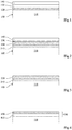
- the figures 1 to 4 are sectional views, partial and schematic, showing steps of an embodiment of a method of manufacturing a contact point on a region comprising germanium.
- the method is implemented during the manufacture of an electronic device comprising one or more components comprising germanium or based on germanium.
- the device can comprise, or be constituted by, an electronic chip of an integrated circuit.
- Such a chip is defined by a portion of a semiconductor wafer and elements, such as electronic components, integrally located in and on one face of the wafer.
- the method can be implemented for the manufacture of a photodiode comprising germanium.
- a substrate 100 is provided.
- the substrate 100 may consist of a portion of a semiconductor wafer, for example made of germanium.
- the substrate 100 can also be formed by a layer covering the upper face of a support such as, for example, a semiconductor wafer.
- a semiconductor region 110 comprising germanium is located on the side of one face of the substrate 100, for example the front or upper face of the substrate 100.
- the region 110 is for example a doped region of the substrate.
- the semiconductor region 110 may have been formed for example in a cavity etched in the substrate 100.
- the semiconductor region 110 is monocrystalline, the substrate 100 preferably being monocrystalline. The semiconductor region 110 can then result from an epitaxy.
- the region 110 consists mainly, that is to say mainly, of germanium.
- the region 110 consists of a semiconductor material having an atomic percentage of germanium greater than 50%, preferably greater than 90%.
- region 110 consists of germanium, for example doped. More preferably, the region 110 is made of germanium monocrystalline.
- region 110 consists of silicon-germanium, for example doped.
- a semiconductor layer 120 having an atomic percentage of silicon greater than 70% is formed on the semiconductor region 110.
- Layer 120 may comprise, in addition to silicon, a metalloid other than silicon, preferably germanium.
- the layer 120 is made of silicon.
- the layer 120 consists of silicon-germanium.
- the semiconductor layer 120 is monocrystalline.
- the layer 120 can be obtained by epitaxy on the monocrystalline region 110.
- the thickness of the semiconductor layer 120 is less than a thickness threshold allowing the epitaxial layer to be monocrystalline.
- This thickness threshold can be determined experimentally as a function of the composition of the semiconductor layer 120 and of the semiconductor region 110. This threshold is of the order of 2 nm for a silicon layer 120 epitaxied on the germanium region 110.
- the semiconductor layer 120 is not single crystal. The thickness of the layer 120 can then be greater than the thickness threshold.
- the metallic layer 130 comprises nickel, for example consists substantially of nickel, for example consists of nickel.
- the layer 130 comprises, in addition to the nickel, platinum and / or cobalt.
- the metal of layer 130 comprises, more preferably consists of, nickel and cobalt, the atomic percentage of cobalt being between 5 and 20%.
- the metal of the layer 130 comprises, more preferably consists of, nickel and platinum, the atomic percentage of platinum being between 5 and 15%.
- the thickness of the metal layer 130 is greater than half that of the semiconductor layer 120. More preferably, the metal layer 130 has a thickness between 7 and 50 nm.
- the upper surface of the semiconductor layer 120 has been prepared beforehand.
- the surface preparation step comprises, for example, a liquid phase treatment based on hydrofluoric acid. , followed by plasma treatment.
- the plasma may be argon-based, or, for example, of the type known under the trade name Siconi TM.
- the plasma treatment and the deposition of the metal layer 130 are then carried out successively without breaking the vacuum. This makes it possible to avoid the presence of impurities, such as oxides, between the semiconductor 120 and metallic layers 130. Such impurities could come from exposure to air after the step of depositing the layer 120, or after the liquid phase surface preparation step.
- the semiconductor 120 and metallic 130 layers are therefore in direct contact with one another.
- a protective layer 140 is formed on the layer 130.
- This layer is then preferably formed without breaking the vacuum after the deposition of the metallic layer 130.
- the layer 140 is intended to protect the structures located under the layer 140 against oxidation during subsequent process steps.
- the protective layer 140 is made of titanium nitride. Alternatively, the protective layer 140 can be omitted.
- a first heat treatment is carried out. More precisely, this treatment thermal corresponds to an annealing of the structure obtained from the figure 1 .
- This first heat treatment is carried out at a temperature making it possible to partially react the metal of the metal layer 130 with the material of the semiconductor layer 120. A layer 220 is thus obtained in place of the layer 120.
- the temperature of the first heat treatment is preferably less than or equal to 300 ° C, for example between 250 ° C and 300 ° C, which allows a partial reaction of the layer 130 comprising nickel with the material of the semiconductor layer 120.
- the first heat treatment is carried out in the presence of dinitrogen.
- the dinitrogen is preferably at atmospheric pressure or at a pressure less than 1 bar above atmospheric pressure.
- the duration of the first heat treatment is preferably between 10 s and 120 s.
- the layer 220 comprises, preferably consists of, an intermetallic material, or intermetallic compound, that is to say the association of one or more metallic chemical elements and one or more chemical elements, typically metalloid, which can enter into the composition of a semiconductor.
- the intermetallic material has a crystalline structure combining metallic and non-metallic chemical elements.
- the non-metallic chemical elements are substantially constituted by the material of the semiconductor layer 120.
- the intermetallic material of the layer 220 is a nickel silicide or a silicide comprising nickel.
- the intermetallic material of layer 220 is a nickel germano-silicide or a germano-silicide comprising nickel.
- the thickness of the metal layer 130 chosen at the stage of figure 1 is sufficient for a portion of the metal in layer 130 to react with an upper portion of semiconductor region 110.
- This reaction produces a layer 210 located below layer 220.
- Layer 210 preferably comprises an intermetallic material. . Because region 110 is mostly germanium, the non-metallic atoms in layer 210 are mostly germanium atoms. Thus, when the metallic layer 130 is made of nickel or comprises nickel, the intermetallic material of the layer 210 is of nickel germanide or of a germanide comprising nickel.
- the thickness of the metal layer 130 chosen at the stage of figure 1 is sufficient so that part 230 of the metal layer 130 does not react with the semiconductor layer 120 and the semiconductor region 110.
- the possible protective layer 140 is removed, as well as the part 230 of the layer 130 which has not reacted.
- This removal is selective with respect to the material of the layer 220.
- the removal is for example carried out in an etching solution based on sulfuric acid and on hydrogen peroxide, or for example in an etching solution with base of hydrochloric acid and nitric acid. Due to the fact that the layer 220 comprises, apart from the metallic elements, more than 70 atom% of silicon, these solutions make it possible to etch the materials of the layers 130 and 140 without removing or altering the layer 220.
- a second heat treatment is carried out.
- This heat treatment corresponds to an annealing of the structure obtained at the stage of figure 3 .
- the temperature of the heat treatment is preferably greater than or equal to 390 ° C. This allows that, after the second heat treatment, the phase of the intermetallic material of the layer 420 has an electrical resistivity lower than that of the other phases of this intermetallic. In particular, this allows the layer 420 to comprise the same proportion of metallic atoms as of non-metallic atoms, for example to comprise the same atomic proportions of nickel and of silicon (NiSi).
- NiSi nickel and of silicon
- the layer 210 is not formed during the first heat treatment, and only the layer 410 is formed during the second heat treatment.
- the heat treatment temperature is preferably less than 420 ° C. This makes it possible to optimize the resistivity of the nickel germanide of the layer 410, and to avoid deteriorating this resistivity by too high a temperature.
- the intermetallic zones defined by the layers 410 and 420 thus obtained constitute an electrical contact point 400 on the semiconductor region 110.
- the presence of the layer 420 makes it possible to obtain a contact socket 400 on the germanium having better resistivity and reliability than a contact socket without such a layer.
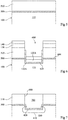
- the figures 5 to 7 are sectional views, partial and schematic, showing steps of another embodiment of a method of manufacturing a contact point on a semiconductor region 110 comprising germanium.
- the semiconductor region 110 is the same or similar to that described in relation to the figure 1 , and is preferably located in the upper part of a substrate 100.
- a semiconductor layer 500 comprising silicon is formed on the upper surface of the semiconductor region 110.
- Layer 500 is made of silicon, or has an atomic percentage of silicon greater than 70%.
- the layer 500 is grown by epitaxy on the surface of the semiconductor region 110.
- the thickness of the layer 500 is for example between 1 nm and 3 nm, preferably of the order of 2 nm. .
- the insulating layer 510 may be made of silicon oxide, preferably of silicon dioxide, more preferably resulting from hydrolysis of tetraethyl orthosilicate (TEOS).
- TEOS tetraethyl orthosilicate
- the silicon oxide insulating layer 510 is a passivation layer.
- the thickness of the insulating layer 510 is of the order of, or greater than, 100 nm.
- an opening 600 is etched through the insulating layer 510 right through to the location of the future contact point.
- the opening 600 is made only above a part of the semiconductor region 110.
- the width of the opening can be between 300 nm and 1.5 ⁇ m.
- the opening 600 is compatible with any usual process for obtaining an opening in an insulating layer, for example photolithography followed by plasma etching (the etching mask is not shown).
- the opening 600 is extended through the layer 500 to a level located in the semiconductor region 110.
- the level difference that is to say the distance in the direction orthogonal to the upper face of the substrate. 100, between the bottom 602 of the opening 600 and the upper face 604 of the semiconductor layer 500, is for example between 5 nm and 30 nm, preferably of the order of 10 nm.
- a semiconductor layer 120A is then grown by epitaxy.
- the layer 120A is identical in composition and thickness to the semiconductor layer 120 of the process. figures 1 to 4 .
- the semiconductor layer 120A grows from the bottom 602 and the portions of the side walls of the opening 600 located below the upper level 604 of the layer 500.
- the semiconductor region defined by the layer 120A forms, together with the portions remaining of the layer 500, a continuous semiconductor layer, that is to say one devoid of openings, covering the semiconductor region 110, this continuous layer comprising at least 70% silicon.
- the metallic 130 and possibly protective 140 layers are successively formed, described in relation with the figure 1 .
- the layers 130 and 140 cover the bottom of the opening 600 and the remaining portions of the insulating layer 510.
- the total thickness of the metallic 130 and protective layers 140 is less than that of the insulating layer 510.
- the metallic 130 and protective 140 layers are formed by non-conforming deposition, that is to say that the materials of these layers are deposited only on the surfaces facing upwards. Because the thickness of the metal layer 130 is less than that of the insulating layer 510, there results a metal region 130A without contact with the rest of the layer 130, and located at the bottom of the opening 600.
- the step described here is not limiting, and one can use any method making it possible to form a metallic region 130A on only part of the semiconductor region 110.
- the metallic 130 and / or protective 140 layers can be formed by conformal deposition. .
- a contact point comprising an intermetallic zone 420 formed from the semiconductor layer 120A.
- the non-metallic atoms of the zone 420 more than 70% are silicon atoms.
- the non-metallic atoms in area 420 are silicon atoms.
- zone 420 comprises nickel silicide.
- the metallic layer 130 is chosen sufficiently thick to form, under the zone 420, an intermetallic zone 410, in which the non-metallic atoms are mainly germanium. More preferably, the zone 410 comprises, for example consists of, nickel germanide.
- the opening 600 is filled with an electrical conductor 700.
- the conductor 700 makes it possible to establish an electrical connection with the semiconductor region 110.
- the conductor 700 may be covered with, and in contact with, a connecting track. electrical between components of an electronic chip.
- the figures 8 to 10 are sectional views, partial and schematic, showing steps of another embodiment of a method of forming a localized contact zone on a semiconductor region 110 comprising germanium.
- the semiconductor region 110 is identical to that described in relation to the figure 1 .
- the semiconductor region 110 is preferably located on the front face side of a substrate 100.
- the semiconductor region 110 is covered with a multilayer 800 comprising, alternately, layers 802 of silicon and layers 804 of germanium. More precisely, the layers 802 have an atomic proportion of silicon greater than 70%. Preferably, the layers 802 are made of silicon, or of silicon-germanium having an atomic proportion of silicon greater than 70%.
- the layers 804 are made of germanium or consist mainly of germanium. Preferably, the layers 804 are made of germanium, or of silicon-germanium consisting mainly of germanium.
- the thickness of the multilayer 800 is greater than 10 nm, preferably of the order of 15 nm.
- the layers 802 have the same thickness.
- the layers 804 have the same thickness. More preferably, the layers 802 and 804 all have the same thickness.
- the multilayer 800 is formed by epitaxy on the upper surface of the single crystal region 110.
- Each of the layers 802 and 804 then has a thickness less than a thickness threshold below which the layer remains single crystal.
- this threshold or critical thickness, depends on the composition of the layers 802 and 804.
- each of the layers 802 and 804 has a thickness of the order of, or less than, 2 nm.
- the multilayer 800 obtained is monocrystalline.
- the opening 600 is formed. extend up to a level located inside the multilayer 800.
- the bottom of the opening 600 is located in a layer 804A among the layers 804 consisting mainly of germanium.
- the bottom of the opening 600 terminates inside one of the layers 802, or at an interface between one of the layers 802 and one of the layers 804. At least one of the layers 802 comprising at least 70% silicon is not reached through opening 600 and is therefore left intact.
- two of the layers 802 are not etched.
- the steps of the figures 2 and 3 that is to say the first heat treatment, and the removal of the possible protective layer 140 and the remains of the metallic layer 130.
- the thickness of the metallic layer 130 deposited in the step of the figure 8 is chosen sufficient so that each of the layers 802 and 804, as well as a part of the semiconductor region 110, react with the metal of the metallic layer 130.
- the reaction of each of the layers 802, 804 with the material of the metallic region 130A produces a zone 902 under the opening 600.
- the parts of the structure located between the zones 902 and the rest of the multilayer 800, delimited in the figure by dotted lines 910, are not shown.
- the layer 904A (shown in dotted lines), which results from the reaction of the layer 804A with the material of the metallic layer 130, is also removed.
- This removal is preferably carried out with the same etching solution as that used to remove the particles. remaining parts of the metal region 130A.
- the non-metallic atoms in zone 904A are mainly germanium atoms. This makes it possible to avoid keeping zone 904A which would have been damaged by the etching solution.
- the upper face of the zone 902 which was under and in contact with the zone 904A before the withdrawal is thus made accessible. Because more than 70%, or all, of the non-metallic atoms in area 902 are silicon, the etching solution leaves area 902. Area 902 is therefore not damaged by etching.
- the semiconductor region 110 is protected from the etching solution by at least one of the zones 902.
- the remainder of the cavity of the opening 600 is then filled with an electrical conductor 700, preferably metallic.
- the zone 1002 located in the upper part of the contact point is in electrical contact with the conductor 700. Because the zone 902 ( figure 9 ) upper has not been altered upon removal of unreacted portions of metallic layer 130, and due to the fact that there is no intermetallic zone from zone 904A between zone 1002 and the conductor electric 700, the resistance and reliability of the contact between the contact point and the conductor 700 are optimized.
- the entire contact point and the semiconductor region 110 is single crystal.
- the electrical resistance of the contact point is lower than that of a non-monocrystalline contact point. This allows a further improvement in electrical resistance.
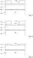
- the figures 11 to 15 are sectional views, partial and schematic, showing successive steps of an embodiment, in the example of the second embodiment ( figures 5 to 7 ), a method of forming an opening in the insulating layer covering a semiconductor region comprising germanium. More precisely, the method is applied here to the formation, from the structure obtained at the stage of figure 5 , with an opening 600 ( figure 6 ) in the insulating layer 510 covering the semiconductor region 110.
- the layer 510 is preferably made of silicon oxide, more preferably of silicon dioxide, even more preferably resulting from hydrolysis of TEOS.
- the layer 510 can also be made of a silicon nitride.
- an additional semiconductor layer 500 is located under the insulating layer 510. More precisely, the semiconductor layer 500 is located between the semiconductor region 110 and the insulating layer 510. The semiconductor layer 500 is in contact with the insulating layer 510.
- the layer 500 consists of silicon, or has an atomic percentage of silicon greater than 70%, the layer 500 then being for example made of silicon-germanium. The silicon layer 500 in contact with the insulating layer 510 then makes it possible to improve the stability of the insulating layer 510, relative to a structure devoid of the layer 500.
- a first masking layer 1110 is formed on the insulating layer 510.
- masking layer is meant a layer intended to be traversed by one or more through openings and to be used during an etching step to allow reagents to pass. engraving only through these openings.
- the first masking layer 1110 is made of a dielectric material, that is to say electrically insulating material.
- a dielectric material that is to say electrically insulating material.
- One advantage is that such a material can be left in place on the insulating layer 510 without creating a short-circuit between future conductive elements in contact with the first masking layer 1110. A step of removing the first layer is thus avoided. masking 1110.
- a second masking layer 1120 comprising an opening 1122 is then formed on the first masking layer 1110.
- the opening 1122 is located directly above the location of the future opening 600.
- the second masking layer 1120 is formed. polymer, and preferably results from the lithography of a positive or negative resin such as a photosensitive resin.
- the etching is etched in the first masking layer 1110 a through opening 1210 located in the extension of the opening 1122 of the second masking layer 1120.
- the etching preferably stops on the upper surface of the insulating layer 510.
- the etching stops at a level located in the insulating layer 510.
- a possible step of removing etching residues (not shown), that is to say a cleaning step, can then be implemented.
- the cleaning is carried out with a solution of hydrofluoric acid HF.
- the second masking layer is removed by oxygen-based etching, typically by plasma.
- the plasma comprises only oxygen or comprises, in addition to oxygen, carbon tetrafluoride CF 4 .
- the temperature during etching is typically between 120 and 220 ° C.
- Such a plasma makes it possible to remove the second masking layer 1120 when it results from lithography or from any method of forming a masking layer comprising openings and removable by oxygen-based etching.
- the opening 600 is formed in the extension of the opening 1210 of the first layer masking 1110, by fluorine-based etching, that is to say etching mainly by one or more reagents comprising fluorine.
- the term “mainly” is understood to mean that more than half, preferably more than 90%, even more preferably more than 99% of the reactive molecules used for the etching are fluorinated.
- the etching is substantially in the absence of oxygen, that is to say that less than 5%, preferably less than 1% of the reactive molecules used for the etching are oxygen O 2 .
- less than 5%, more preferably less than 1% of the reactive molecules used for the etching comprise oxygen.
- the etching reagent (s) are devoid of oxygen.
- the etching is a reactive ion etching RIE (Reactive Ion Etching), for example by octafluorocyclobutane C 4 F 8 and / or by trifluoromethane CHF 3 .
- RIE reactive Ion Etching
- the first masking layer 1110 is in the group consisting of HfO 2 , Al 2 O 3 , AlN, ZnO, SiN, and Si 3 N 4 allows the material of the insulating layer to be selectively etched. 510 with respect to the material of the first masking layer 1110.
- the etching speed of the insulating layer 510 is then more than 5 times faster than the etching speed of the masking layer material.
- the first masking layer is made of HfO 2 or Al 2 O 3 , and the etching rate of the silicon oxide resulting from a hydrolysis of TEOS is then more than 10 times greater. faster than the etching speed of the material of the first masking layer.
- etching residues 1410 may remain on the sides and the bottom of the opening 600. can then provide a cleaning step described below in relation to the figure 15 .
- the etching residues 1410 are removed.
- an HF solution is used.
- the solution preferably has an HF concentration of between 0.1% and 1 mol%, and is applied for a period of between 10 to 30 s.
- the opening 600 in the insulating layer 510 covering the semiconductor region 110 is obtained.
- the thickness, mentioned above, of the layer 500 would then have been too small to prevent the layer 500 from being oxidized over its entire thickness, and that part of the germanium in the semiconductor region 110 also be oxidized. This would have resulted in an extension of the opening 600 below the lower level of the insulating layer 510, as mentioned above in relation to the figures 6 and 8 .
- the steps of figures 11 to 15 allow the insulating layer 510 to protect the semiconductor layer 500 from oxidation during removal of the polymer masking layer. In particular, this makes it possible to leave in place a region 120A of the semiconductor layer 500 at the bottom of the opening. This also makes it possible to form the opening 600 without oxidizing the germanium of the semiconductor region 110. This prevents the semiconductor region 110 from being damaged by the oxidation.
- the stages of figures 11 to 15 are implemented here in the example of the formation of the opening 600 in the insulating layer 510, steps similar to those of figures 11 to 15 can be implemented to form any opening in any insulating layer covering a semiconductor region consisting mainly of germanium, the insulating layer preferably being made of silicon oxide and more preferably of silicon oxide resulting from the hydrolysis of TEOS.
- the layer 500 can be omitted.
- the insulating layer may be made of silicon nitride, the person skilled in the art then being able to define the material of the first masking layer in order to obtain a selective fluorinated-based etching of the silicon nitride with respect to the layer of masking.
- the figure 16 is a sectional view, partial and schematic, showing a fourth embodiment of a method of manufacturing a contact point, implementing the steps of figures 11 to 15 .
- a contact point 400 comprising an intermetallic zone 420 formed from the semiconductor region 120A ( figure 6 ).
- the intermetallic zone results from the reaction of a 130A region ( figure 6 ) of the metal layer 130 with the semiconductor region 120A.
- the stages of figures 11 to 15 prevent the semiconductor region 110 from being damaged by oxidation.
- the semiconductor region 110 is preferably doped. Now, the higher the doping level of the semiconductor region 110, the more this region is sensitive to oxidation, this more particularly for doping resulting from ion implantation.
- the resulting contact socket 400 thus has lower resistance and higher reliability than that of a contact socket for which the opening 600 has been formed by a single layer masking process.
- region 120A which forms the intermetallic zone 420 by reaction with the metallic region 130A, is formed by a part of the semiconductor layer 500. Since the semiconductor layer 500 has an atomic percentage of silicon greater than 70%, more than 70 % of non-metallic atoms in intermetallic zone 420 are silicon atoms. As a variant, region 120A comprises, or is constituted by, a semiconductor layer formed on the portion of semiconductor layer 500, or, in the absence of semiconductor layer 500, directly on semiconductor region 110.
- the electrical conductor 700 is preferably obtained by forming a metal layer over the entire upper surface of the structure.
- the parts of the metal layer located above the upper level of the first masking layer 1110 are then removed. This removal is for example carried out by mechanical-chemical polishing.
- the first masking layer 1110 can then advantageously serve as a barrier layer.
- the first masking layer is made of an electrically insulating material that can be left in place, this is not limiting.
- the first masking layer 1110 and the metallic region 130A comprise, preferably consist of, one or more of the same metals.
- the first masking layer 1110 can advantageously be removed at the same time as the portions of the metallic layer 130 remaining after the formation of the contact point.
- the first masking layer 1110 and the protective layer 140 ( figure 6 ) covering the metallic region 130A comprise, preferably consist of, one or more of the same metals.
- the first masking layer 1110 can advantageously be removed at the same time as the protective layer 140.
- the figure 17 is a sectional view, partial and schematic, showing a variant of implementation of the method of figures 11 to 15 .
- the variant of figure 17 corresponds to the process of figures 11 to 15 in which, at the stage of figure 14 , the fluorinated-based etching is, at least in part, carried out by an HF solution.
- the HF solution preferably has a higher concentration than that of the HF solution used in the cleaning step of the figure 15 , for example greater than 5 mol%.
- Such an etching is substantially isotropic.
- the opening 600 in the insulating layer is wider than the opening 1112 in the first masking layer 1110. In other words, the sidewalls 1710 of opening 600 are overhung by the edges of opening 1112.
- the layer 510 is made of silicon nitride
- the fact of providing that the layer 510 is made of silicon oxide advantageously allows the fluorinated-based plasma etching to be easier and / or that the shapes of the sides and the dimensions of the opening 600 are better controlled.
- the fluorinated-based etching stage can be followed by a cleaning stage corresponding to the stage of figure 15 .
- the figures 18 and 19 are sectional views, partial and schematic, showing steps of a variant of the fourth embodiment, implementing the variant of the figure 17 .
- the metal layer 130 is formed and, preferably, the protective layer 140, in the manner described in relation to the figure 6 .
- the metallic layer 130 includes a metallic region 130A for reacting with the semiconductor region 120A to form an intermetallic region. Due to the overhanging shape of the walls of the openings 600 and 1112, the metallic region 130A is advantageously separated from the rest of the layer 130, which facilitates the subsequent removal of the remaining parts of the layer 130 after reaction.
- a contact point is formed comprising intermetallic zones 410 and preferably 420, and the opening 600 is filled with a conductor 700, in the manner described in relation to the figure 7 .
- the figure 20 is a sectional view, partial and schematic, showing a fifth embodiment of a method of manufacturing a contact point, implementing the variant of the figure 17 .
- the fifth embodiment differs from the second embodiment ( figures 5 to 7 ) in that, at the stage of figure 7 , an electrically conductive layer 2010 covering the contact socket 400 is formed on the bottom and the sides of the opening 600 before the opening 600 is filled by the conductor 700.
- the electrically conductive layer 2010 is preferably made of titanium nitride TiN.
- the electrically conductive layer 2010 is in contact with the intermetallic zone 420.
- the thickness of the electrically conductive layer 2010 is preferably between 5 and 20 nm.
- the electrically conductive layer 2010 makes it possible to protect the upper surface of the contact socket 420, in particular against a diffusion of the material of the conductor 700 towards the intermetallic zone and / or against an oxidation in the case where the structure is exposed to air. before filling of the opening 600 by the conductor 700. The resistance is thus reduced and the reliability of the contact is increased, compared to a contact not covered with the conductive layer 2010.
- the layer 2010, being electrically conductive also makes it possible to make an electrical contact between the contact point and the conductor 700.
- the figure 21 is a sectional view, partial and schematic, showing an embodiment of a photodiode 2100. More precisely, the method of manufacturing the photodiode 2100 here implements the fifth embodiment of the method of manufacturing a socket. contact. The manufacturing process of the photodiode is compatible with the various embodiments, described above, of contacts.
- the substrate 100 is preferably made of germanium.
- the germanium of the substrate 100 is intrinsic, that is to say not intentionally doped or having a doping level less than 10 16 atoms / cm 3 , preferably less than or equal to 10 15 atoms / cm 3 .
- the germanium of the substrate 100 is preferably monocrystalline.
- the substrate 100 can be made of silicon-germanium, preferably intrinsic and monocrystalline.
- the substrate 100 covers a semiconductor wafer 2110 of silicon. More precisely, an insulating layer 2120, typically made of silicon oxide, is placed between the semiconductor wafer 2110 and the substrate 100.
- the semiconductor wafer 2110, the insulating layer 2120, and the substrate 100 thus define an SOI (Semiconductor On) type structure. Insulator), more specifically, a GeOI (Germanium On Insulator) structure.
- the thickness of the insulating layer 2120 is typically of the order of 0.1 to 1 ⁇ m.
- the total thickness of the substrate 100 is for example of the order of 1 to 2 ⁇ m.
- a semiconductor region 110P of P-doped germanium is formed, and a semiconductor region 110N of doped germanium of type N.
- the semiconductor regions 110N and 110P are of opposite conductivity types.
- the semiconductor regions 110N and 110P extend from the free or accessible face of the substrate 100, that is to say from the front face (upper face in the orientation of the figure).
- Semiconductor regions 110N and 110P constitute respective cathode and anode regions of photodiode 2100.
- the semiconductor regions 110P and 110N are obtained by forming cavities in the substrate 100 at the locations of the semiconductor regions 110P and 110N, then filling the cavities by epitaxy with doped germanium. This allows the semiconductor regions to be, at least in an upper part intended for the formation of the contact points, monocrystalline.
- the semiconductor regions 110N and 110P are obtained by ion implantation.
- a semiconductor region 100I of the substrate 100 separates the semiconductor regions 110P and 110N.
- the semiconductor region 100I is thus made of intrinsic germanium.
- the distance separating the semiconductor regions 110P and 110N is between 1 ⁇ m and 20 ⁇ m.
- a silicon-germanium layer 2130 is formed on the structure and in particular on the intrinsic region 100I.
- the silicon-germanium layer 2130 is preferably formed by epitaxy on the substrate 100, more precisely on the free face of the substrate 100.
- the silicon-germanium layer 2130 is thus in contact with the substrate 100.
- the silicon-germanium layer 2130 preferably has a thickness less than the critical thickness below which the silicon-germanium layer 2130 remains monocrystalline during its growth by epitaxy.
- the thickness of the silicon-germanium layer 2130 is typically less than 3 nm.
- the semiconductor layer 500 is then formed on the silicon-germanium layer 2130. More preferably, before forming the semiconductor layer 500, an intrinsic germanium layer 2140 is formed on the silicon-germanium layer 2130.
- the silicon-germanium layer 2130. germanium 2140 allows in particular that the semiconductor 500 is monocrystalline.
- the semiconductor layer 500 has a sufficiently low thickness, mentioned above. Indeed, in the absence of the germanium layer 2140, the sum of the thicknesses of the silicon-germanium layer 2130 and of the semiconductor layer 500 would be too high for the semiconductor layer 500 to remain monocrystalline.
- the insulating layer 510 is then formed, then, in the example shown, the fourth embodiment ( figure 20 ) of the handshake training process. More precisely, the method is implemented to simultaneously form two contacts 400N and 400P with the respective semiconductor regions 110N and 110P.
- Each contact 400N, 400P thus comprises an intermetallic zone 420, in which more than 70% of the non-metallic atoms are silicon atoms, and, preferably, an intermetallic zone 410, in which the non-metallic atoms are mainly germanium atoms. .
- the edges of the contact points are not shown (regions between dotted lines 2150).
- the contact point may further comprise an intermetallic zone 2132 located on and in contact with the intermetallic zone 410.
- the intermetallic zone 2132 comprises silicon atoms and germanium atoms.
- the contact point may further comprise an intermetallic zone 2142, in which the non-metallic atoms are mainly, preferably are only, germanium atoms. Intermetallic zone 2142 is between zones 2132 and 420.
- the silicon-germanium layer 2130 located between the semiconductor region 110I and the insulating layer 510, is in contact. with the intrinsic region 100I. This makes it possible to obtain a monocrystalline interface delimiting the semiconductor region 110I. Such an interface makes it possible to reduce the dark current of the photodiode, compared with an interface exhibiting crystalline defects.
- the germanium layer 2140 is located between the silicon-germanium layer 2130 and the insulating layer 510, preferably between the silicon-germanium layer 2130 and the semiconductor layer 500. Because the silicon-germanium has a bandgap (band gap) wider than that of germanium, carriers present in the germanium layer 2140 cannot access the intrinsic region 110I.
- These carriers can for example come from defects at the interface of the semiconductor layer 500 with the insulating layer 510 and / or the germanium layer 2140. Because the layers 2130 and 2140 make it possible to prevent these carriers from reaching the region. intrinsic 100I, the dark current of the photodiode is reduced compared to the dark current of a photodiode without layers 2130 and / or 2140.
- the figure 22 is a sectional view, partial and schematic, showing another embodiment of a photodiode 2200.
- the method of manufacturing the photodiode 2200 differs from that of the photodiode 2100 of the figure 21 in that, before formation of the insulating layer 510, insulating trenches 2210 have been formed delimiting, on the intrinsic region 100I, a portion 2240 of the germanium layer 2140.
- the insulating trenches 2210 are located plumb edges of the intrinsic region 100I.
- the insulating trenches are then filled with an electrical insulator, preferably the insulator of the layer 510.
- the trenches 2210 have a width of between 100 nm and 300 nm.
- the trenches extend from the upper face of the semiconductor layer 500, through layers 500 and 2140, up to the upper face of the silicon-germanium layer 2130.
- the trenches 2210 extend through the layer 2130, for example at least up to the face top of the substrate 100.
- the trenches 2210 thus constitute insulating zones delimiting a portion of the germanium layer 2140 on the intrinsic region 100I. These insulating zones are located between the germanium layer 2140 and the 400N and 400P contact points.
- the photodiode 2200 is compatible with any process for forming an intrinsic germanium layer located on the intrinsic region 100I and delimited by insulating zones located between said germanium layer 2140 and the contact points.
- the germanium layer 2140 can be formed only on the intrinsic region 100I.
- the insulating zones 2210 make it possible to prevent the carriers present in the germanium layer 2140, mentioned above, from reaching the 400N and 400P contact points.
- the insulating areas allow the photodiode 2200 to exhibit a lower dark current than that of a photodiode, such as the photodiode 2100 of the figure 21 , devoid of insulating zones 2210.
Abstract
La présente description concerne un procédé de formation d'une ouverture (600) dans une couche isolante (510) recouvrant une région semiconductrice (110) comportant du germanium, comprenant successivement : la formation d'une première couche de masquage (1110) sur la couche isolante (510) ; la formation sur la première couche de masquage (1110) d'une deuxième couche de masquage comprenant une ouverture ; la gravure d'une ouverture dans la première couche de masquage, dans le prolongement de l'ouverture de la deuxième couche de masquage ; le retrait de la deuxième couche de masquage par gravure à base d'oxygène ; et la formation de l'ouverture (600) de ladite couche isolante (510) dans le prolongement de l'ouverture de la première couche de masquage, par gravure à base fluorée.The present description relates to a method of forming an opening (600) in an insulating layer (510) covering a semiconductor region (110) comprising germanium, comprising successively: forming a first masking layer (1110) on the insulating layer (510); forming on the first masking layer (1110) a second masking layer comprising an opening; etching an opening in the first masking layer, in the extension of the opening of the second masking layer; removing the second masking layer by oxygen-based etching; and forming the opening (600) of said insulating layer (510) in the extension of the opening of the first masking layer, by fluoride-based etching.
Description
La présente description concerne de façon générale les dispositifs électroniques, et plus particulièrement des composants électroniques comprenant du germanium et les procédés de fabrication de composants électroniques.The present description relates generally to electronic devices, and more particularly to electronic components comprising germanium, and to methods of manufacturing electronic components.
Certains composants électroniques, tels que des transistors, des diodes, etc., utilisent les propriétés du germanium. Par exemple, une photodiode de type PIN, c'est-à-dire une photodiode comprenant une région semiconductrice intrinsèque entre des régions semiconductrices dopées de types N et P, peut-être basée sur du germanium. La photodiode peut alors détecter des rayonnements optiques de longueurs d'onde comprises entre 0,9 µm et 1,5 µm.Some electronic components, such as transistors, diodes, etc., use the properties of germanium. For example, a PIN type photodiode, that is to say a photodiode comprising an intrinsic semiconductor region between doped semiconductor regions of N and P types, perhaps based on germanium. The photodiode can then detect optical radiation of wavelengths between 0.9 µm and 1.5 µm.
Dans un tel composant, une région comprenant du germanium est destinée à être connectée électriquement à d'autres dispositifs par une liaison conductrice. Le contact électrique entre cette région et la liaison conductrice est assuré par une zone de contact, ou prise de contact.In such a component, a region comprising germanium is intended to be electrically connected to other devices by a conductive link. The electrical contact between this region and the conductive connection is provided by a contact zone, or contact point.
La prise de contact est typiquement située au fond d'une ouverture pratiquée dans une couche isolante.The contact point is typically located at the bottom of an opening made in an insulating layer.
Il existe un besoin de réduire les résistances et/ou d'augmenter la fiabilité des prises de contact connues sur une région semiconductrice comprenant du germanium.There is a need to reduce the resistances and / or to increase the reliability of known contact points on a semiconductor region comprising germanium.
Il existe un besoin de simplifier les procédés connus de réalisation de prises de contact sur une région semiconductrice comprenant du germanium.There is a need to simplify the known methods of making contact points on a semiconductor region comprising germanium.
Un mode de réalisation pallie tout ou partie des inconvénients des prises de contact connues avec une région semiconductrice comprenant du germanium.One embodiment overcomes all or part of the drawbacks of known contact points with a semiconductor region comprising germanium.
Un mode de réalisation pallie tout ou partie des inconvénients des procédés connus de réalisation de prise de contact avec une région semiconductrice comprenant du germanium.One embodiment overcomes all or part of the drawbacks of the known methods of making contact with a semiconductor region comprising germanium.
Un mode de réalisation pallie tout ou partie des inconvénients des procédés de gravure d'une ouverture dans un isolant recouvrant une région semiconductrice comprenant du germanium.One embodiment overcomes all or part of the drawbacks of the methods for etching an opening in an insulator covering a semiconductor region comprising germanium.
Un mode de réalisation pallie tout ou partie des inconvénients des photodiodes connues de type PIN comprenant une région intrinsèque de germanium. En particulier, un mode de réalisation prévoit une photodiode présentant un courant d'obscurité réduit.One embodiment overcomes all or part of the drawbacks of known PIN-type photodiodes comprising an intrinsic region of germanium. In particular, one embodiment provides a photodiode exhibiting a reduced dark current.
Ainsi, selon un premier aspect, un mode de réalisation prévoit un procédé de formation d'une prise de contact électrique avec une région semiconductrice constituée principalement de germanium, comprenant la formation d'une première zone constituée d'un premier matériau intermétallique dans lequel plus de 70 % des atomes non métalliques sont de silicium.Thus, according to a first aspect, an embodiment provides a method of forming an electrical contact with a semiconductor region consisting mainly of germanium, comprising forming a first region consisting of a first intermetallic material in which more 70% of non-metallic atoms are silicon.
Un mode de réalisation prévoit un dispositif électronique comprenant une région semiconductrice constituée principalement de germanium, et une prise de contact électrique avec la région semiconductrice, la prise de contact comprenant une première zone constituée d'un premier matériau intermétallique dans lequel plus de 70 % des atomes non métalliques sont de silicium.One embodiment provides an electronic device comprising a semiconductor region consisting mainly of germanium, and an electrical contact with the semiconductor region, the contact comprising a first region made of a first intermetallic material in which more than 70% of Non-metallic atoms are silicon.
Selon un mode de réalisation, la prise de contact comprend, entre la première zone et la région semiconductrice, une deuxième zone constituée d'un deuxième matériau intermétallique dans lequel les atomes non métalliques sont principalement de germanium.According to one embodiment, the contact point comprises, between the first zone and the semiconductor region, a second zone consisting of a second intermetallic material in which the non-metallic atoms are mainly germanium.
Selon un mode de réalisation, les atomes métalliques de chacun des premier et deuxième matériaux intermétalliques sont principalement de nickel.According to one embodiment, the metal atoms of each of the first and second intermetallic materials are mainly nickel.
Selon un mode de réalisation, chacun des premier et deuxième matériaux intermétalliques comprend du platine et/ou du cobalt.According to one embodiment, each of the first and second intermetallic materials comprises platinum and / or cobalt.
Selon un mode de réalisation, le premier matériau intermétallique comprend du germanium.According to one embodiment, the first intermetallic material comprises germanium.
Selon un mode de réalisation, la formation de la première zone comprend successivement : a) la formation d'au moins une couche semiconductrice recouvrant la région semiconductrice et comprenant au moins 70 % d'atomes de silicium ; b) la formation d'une région métallique sur ladite au moins une couche semiconductrice ; et c) la réaction de la région métallique avec au moins une partie de ladite au moins une couche semiconductrice.According to one embodiment, the formation of the first zone comprises successively: a) the formation of at least one semiconductor layer covering the semiconductor region and comprising at least 70 atom% of silicon; b) forming a metallic region on said at least one semiconductor layer; and c) reacting the metallic region with at least part of said at least one semiconductor layer.
Selon un mode de réalisation, le procédé comprend en outre la réaction du matériau de la région métallique avec celui de la région semiconductrice.According to one embodiment, the method further comprises reacting the material of the metallic region with that of the semiconductor region.
Selon un mode de réalisation, l'étape c) comprend : un premier traitement thermique, de préférence à une température inférieure à 300°C ; un retrait de parties de la région métallique n'ayant pas réagi au cours du premier traitement thermique ; et un deuxième traitement thermique, de préférence à une température comprise entre 390°C et 420°C.According to one embodiment, step c) comprises: a first heat treatment, preferably at a temperature below 300 ° C; removing unreacted portions of the metallic region during the first heat treatment; and a second heat treatment, preferably at a temperature between 390 ° C and 420 ° C.
Selon un mode de réalisation, le procédé comprend, avant l'étape b), la formation d'une couche de protection, de préférence en nitrure de titane, sur la région métallique.According to one embodiment, the method comprises, before step b), the formation of a protective layer, preferably of titanium nitride, on the metallic region.
Selon un mode de réalisation, le procédé comprend la formation successivement : d'une couche semiconductrice supplémentaire comprenant au moins 70 % d'atomes de silicium ; d'une couche isolante recouvrant la couche semiconductrice supplémentaire ; et d'une ouverture traversant la couche isolante et la couche semiconductrice supplémentaire, ladite au moins une couche semiconductrice étant formée dans l'ouverture et formant, avec les parties de la couche semiconductrice supplémentaire situées autour de l'ouverture, une couche continue.According to one embodiment, the method comprises successively forming: an additional semiconductor layer comprising at least 70 atom% of silicon; an insulating layer covering the additional semiconductor layer; and an opening passing through the insulating layer and the additional semiconductor layer, said at least one semiconductor layer being formed in the opening and forming, with the parts of the additional semiconductor layer located around the opening, a continuous layer.
Selon un mode de réalisation, le procédé comprend successivement la formation : d'un multicouches de premières couches semiconductrices comprenant au moine 70 % d'atomes de silicium alternées avec des deuxièmes couches semiconductrices constituées principalement de germanium ; d'une couche isolante recouvrant le multicouches ; et d'une ouverture traversant la couche isolante et une partie du multicouches, ladite au moins une couche semiconductrice étant constituée des premières couches ayant été laissées intactes sous l'ouverture.According to one embodiment, the method successively comprises forming: a multilayer of first semiconductor layers comprising at least 70% of silicon atoms alternated with second semiconductor layers consisting mainly of germanium; an insulating layer covering the multilayer; and an opening passing through the insulating layer and part of the multilayer, said at least one semiconductor layer consisting of the first layers having been left intact under the opening.
Selon un mode de réalisation, le multicouche est monocristallin.According to one embodiment, the multilayer is monocrystalline.
Un autre mode de réalisation prévoit un procédé de fabrication d'un dispositif électronique, comprenant la mise en oeuvre d'un procédé tel que défini ci-dessus.Another embodiment provides for a method of manufacturing an electronic device, comprising the implementation of a method as defined above.
Un autre mode de réalisation prévoit une photodiode comprenant un dispositif tel que défini ci-dessus ou un dispositif obtenu par un procédé tel que défini ci-dessus.Another embodiment provides for a photodiode comprising a device as defined above or a device obtained by a method as defined above.
Selon un deuxième aspect, un mode de réalisation prévoit un procédé de formation d'une ouverture dans une couche isolante recouvrant une région semiconductrice comportant du germanium, comprenant successivement : a) la formation d'une première couche de masquage sur la couche isolante ; b) la formation sur la première couche de masquage d'une deuxième couche de masquage comprenant une ouverture ; c) la gravure d'une ouverture dans la première couche de masquage, dans le prolongement de l'ouverture de la deuxième couche de masquage ; d) le retrait de la deuxième couche de masquage par gravure à base d'oxygène ; et e) la formation de l'ouverture de ladite couche isolante dans le prolongement de l'ouverture de la première couche de masquage, par une gravure à base fluorée dans laquelle moins de 5 % des molécules réactives utilisées sont des molécules d'oxygène.According to a second aspect, an embodiment provides a method of forming an opening in an insulating layer covering a semiconductor region comprising germanium, comprising successively: a) the forming a first masking layer on the insulating layer; b) forming on the first masking layer a second masking layer comprising an opening; c) etching an opening in the first masking layer, in the extension of the opening of the second masking layer; d) removing the second masking layer by oxygen-based etching; and e) forming the opening of said insulating layer in the extension of the opening of the first masking layer, by fluorine-based etching in which less than 5% of the reactive molecules used are oxygen molecules.
Selon un mode de réalisation, la couche isolante est en oxyde de silicium.According to one embodiment, the insulating layer is made of silicon oxide.
Selon un mode de réalisation, la première couche de masquage est en un matériau électriquement isolant, de préférence dans le groupe constitué de HfO2, Al2O3, AlN, ZnO, SiN, et Si3N4.According to one embodiment, the first masking layer is made of an electrically insulating material, preferably from the group consisting of HfO 2 , Al 2 O 3 , AlN, ZnO, SiN, and Si 3 N 4 .
Selon un mode de réalisation, l'étape e) comprend une gravure par plasma à base de C4F8 et/ou CHF3, et/ou par une solution d'HF.According to one embodiment, step e) comprises etching by plasma based on C 4 F 8 and / or CHF 3 , and / or by an HF solution.
Selon un mode de réalisation, la deuxième couche de masquage est une couche de polymère résultant d'une lithographie.According to one embodiment, the second masking layer is a polymer layer resulting from lithography.
Selon un mode de réalisation, une couche supplémentaire, de préférence en silicium ou ayant un pourcentage atomique de silicium supérieur à 70 %, est située entre ladite région semiconductrice et ladite couche isolante.According to one embodiment, an additional layer, preferably made of silicon or having an atomic percentage of silicon greater than 70%, is located between said semiconductor region and said insulating layer.
Un mode de réalisation prévoit un procédé de formation d'une prise de contact, comprenant la mise en oeuvre d'un procédé tel que défini ci-dessus, la prise de contact étant une prise de contact avec ladite région semiconductrice et comprenant une zone intermétallique dans laquelle plus de 70 % des atomes non métalliques sont de silicium.One embodiment provides a method of forming a contact, comprising the implementation of a method as defined above, the contact being a contact with said semiconductor region and comprising an intermetallic zone in which more than 70% of the non-metallic atoms are silicon.
Selon un mode de réalisation, la formation de ladite zone intermétallique comprend la réaction d'un semiconducteur avec une région métallique, la première couche de masquage et la région métallique comprenant un même métal.According to one embodiment, the formation of said intermetallic zone comprises the reaction of a semiconductor with a metallic region, the first masking layer and the metallic region comprising the same metal.
Selon un mode de réalisation, la formation de la zone intermétallique comprend la réaction d'un semiconducteur avec une région métallique recouverte d'une couche de protection, la première couche de masquage et la couche de protection comprenant un même métal.According to one embodiment, the formation of the intermetallic zone comprises the reaction of a semiconductor with a metallic region covered with a protective layer, the first masking layer and the protective layer comprising the same metal.
Selon un mode de réalisation, le procédé comprend en outre la formation d'une couche électriquement conductrice recouvrant la prise de contact et les parois de l'ouverture, et le remplissage de l'ouverture par un conducteur recouvrant ladite couche électriquement conductrice.According to one embodiment, the method further comprises forming an electrically conductive layer covering the contact point and the walls of the opening, and filling the opening with a conductor covering said electrically conductive layer.
Un mode de réalisation prévoit un procédé de formation d'une photodiode, comprenant la formation, par un procédé tel que défini ci-dessus, de première et deuxième prises de contact respectives avec des première et deuxième régions semiconductrices comprenant du germanium, les première et deuxième régions semiconductrices étant dopées de types de conductivité opposés et séparées par une troisième région semiconductrice comprenant du germanium intrinsèque.An embodiment provides a method of forming a photodiode, comprising the formation, by a method as defined above, of first and second respective contacts with first and second semiconductor regions comprising germanium, the first and the second semiconductor regions comprising germanium. second semiconductor regions being doped with opposite conductivity types and separated by a third semiconductor region comprising intrinsic germanium.
Selon un mode de réalisation, une couche de silicium-germanium est située entre la troisième région et ladite couche isolante et est en contact avec la troisième région.According to one embodiment, a silicon-germanium layer is located between the third region and said insulating layer and is in contact with the third region.
Selon un mode de réalisation, une couche de germanium intrinsèque est située entre ladite couche de silicium-germanium et ladite couche isolante.According to one embodiment, an intrinsic germanium layer is located between said silicon-germanium layer and said insulating layer.
Selon un mode de réalisation, le procédé comprend la formation de zones isolantes délimitant ladite couche de germanium intrinsèque et situées entre ladite couche de germanium intrinsèque et les première et deuxième prises de contact.According to one embodiment, the method comprises the formation of insulating zones delimiting said layer of intrinsic germanium and located between said intrinsic germanium layer and the first and second contact points.
Un mode de réalisation prévoit une photodiode formée par un procédé tel que défini ci-dessus.One embodiment provides for a photodiode formed by a method as defined above.
Ces caractéristiques et avantages, ainsi que d'autres, seront exposés en détail dans la description suivante de modes de réalisation particuliers faite à titre non limitatif en relation avec les figures jointes parmi lesquelles :
- la
figure 1 est une vue en coupe, partielle et schématique, représentant une étape d'un premier mode de réalisation d'un procédé de fabrication d'une prise de contact ; - la
figure 2 est une vue en coupe, partielle et schématique, représentant une autre étape du premier mode de réalisation ; - la
figure 3 est une vue en coupe, partielle et schématique, représentant une autre étape du premier mode de réalisation ; - la
figure 4 est une vue en coupe, partielle et schématique, représentant une autre étape du premier mode de réalisation ; - la
figure 5 est une vue en coupe, partielle et schématique, représentant une étape d'un deuxième mode de réalisation d'un procédé de fabrication d'une prise de contact ; - la
figure 6 est une vue en coupe, partielle et schématique, représentant une autre étape du deuxième mode de réalisation ; - la
figure 7 est une vue en coupe, partielle et schématique, représentant une autre étape du deuxième mode de réalisation ; - la
figure 8 est une vue en coupe, partielle et schématique, représentant une étape d'un troisième mode de réalisation d'un procédé de fabrication d'une prise de contact ; - la
figure 9 est une vue en coupe, partielle et schématique, représentant une autre étape du troisième mode de réalisation ; - la
figure 10 est une vue en coupe, partielle et schématique, représentant une autre étape du troisième mode de réalisation ; - la
figure 11 est une vue en coupe, partielle et schématique, représentant une étape d'un mode de mise en oeuvre, dans l'exemple du deuxième mode de réalisation, d'un procédé de formation d'une ouverture dans une couche isolante recouvrant une région semiconductrice comprenant du germanium ; - la
figure 12 est une vue en coupe, partielle et schématique, représentant une autre étape du mode de mise en oeuvre du procédé de formation d'une ouverture ; - la
figure 13 est une vue en coupe, partielle et schématique, représentant une autre étape du mode de mise en oeuvre du procédé de formation d'une ouverture ; - la
figure 14 est une vue en coupe, partielle et schématique, représentant une autre étape du mode de mise en oeuvre du procédé de formation d'une ouverture ; - la
figure 15 est une vue en coupe, partielle et schématique, représentant une autre étape du mode de mise en oeuvre du procédé de formation d'une ouverture ; - la
figure 16 est une vue en coupe, partielle et schématique, représentant un quatrième mode de réalisation d'un procédé de fabrication d'une prise de contact, mettant en oeuvre les étapes desfigures 11 à 15 ; - la
figure 17 est une vue en coupe, partielle et schématique, représentant une variante de mise en oeuvre du procédé de formation d'une ouverture; - La
figure 18 est une vue en coupe, partielle et schématique, représentant une étape d'une variante du quatrième mode de réalisation, mettant en oeuvre la variante de lafigure 17 ; - La
figure 19 est une vue en coupe, partielle et schématique, représentant une autre étape de la variante du quatrième mode de réalisation ; - la
figure 20 est une vue en coupe, partielle et schématique, représentant un cinquième mode de réalisation d'un procédé de fabrication d'une prise de contact, mettant en oeuvre la variante de lafigure 17 ; - la
figure 21 est une vue en coupe, partielle et schématique, représentant un mode de réalisation d'une photodiode ; - la
figure 22 est une vue en coupe, partielle et schématique, représentant un autre mode de réalisation d'une photodiode.
- the
figure 1 is a sectional view, partial and schematic, showing a step of a first embodiment of a method of manufacturing a contact point; - the
figure 2 is a sectional view, partial and schematic, showing another step of the first embodiment; - the
figure 3 is a sectional view, partial and schematic, showing another step of the first embodiment; - the
figure 4 is a sectional view, partial and schematic, showing another step of the first embodiment; - the
figure 5 is a sectional view, partial and schematic, showing a step of a second embodiment of a method of manufacturing a contact point; - the
figure 6 is a sectional view, partial and schematic, showing another step of the second embodiment; - the
figure 7 is a sectional view, partial and schematic, showing another step of the second embodiment; - the
figure 8 is a sectional view, partial and schematic, showing a step of a third embodiment of a method of manufacturing a contact point; - the
figure 9 is a sectional view, partial and schematic, showing another step of the third embodiment; - the
figure 10 is a sectional view, partial and schematic, showing another step of the third embodiment; - the
figure 11 is a sectional view, partial and schematic, showing a step of an embodiment, in the example of the second embodiment, of a method of forming an opening in an insulating layer covering a semiconductor region comprising germanium; - the
figure 12 is a sectional view, partial and schematic, showing another step of the embodiment of the method for forming an opening; - the
figure 13 is a sectional view, partial and schematic, showing another step of the embodiment of the method for forming an opening; - the
figure 14 is a sectional view, partial and schematic, showing another step of the embodiment of the method for forming an opening; - the
figure 15 is a sectional view, partial and schematic, showing another step of the embodiment of the method for forming an opening; - the
figure 16 is a sectional view, partial and schematic, showing a fourth embodiment of a method of manufacturing a contact point, implementing the steps offigures 11 to 15 ; - the
figure 17 is a partial and schematic sectional view showing an alternative embodiment of the method for forming an opening; - The
figure 18 is a sectional view, partial and schematic, showing a step of a variant of the fourth embodiment, implementing the variant of thefigure 17 ; - The
figure 19 is a sectional view, partial and schematic, showing another step of the variant of the fourth embodiment; - the
figure 20 is a sectional view, partial and schematic, showing a fifth embodiment of a method of manufacturing a contact point, implementing the variant of thefigure 17 ; - the
figure 21 is a sectional view, partial and schematic, showing an embodiment of a photodiode; - the
figure 22 is a sectional view, partial and schematic, showing another embodiment of a photodiode.
De mêmes éléments ont été désignés par de mêmes références dans les différentes figures. En particulier, les éléments structurels et/ou fonctionnels communs aux différents modes de réalisation peuvent présenter les mêmes références et peuvent disposer de propriétés structurelles, dimensionnelles et matérielles identiques.The same elements have been designated by the same references in the various figures. In particular, the structural and / or functional elements common to the different embodiments may have the same references and may have identical structural, dimensional and material properties.
Par souci de clarté, seuls les étapes et éléments utiles à la compréhension des modes de réalisation décrits ont été représentés et sont détaillés. En particulier, dans les composants électroniques, les éléments autres qu'une région semiconductrice comprenant du germanium, une prise de contact, et un conducteur électrique, n'ont pas été décrits, les modes de réalisation étant compatibles avec les composants électroniques connus comportant une région en germanium.For the sake of clarity, only the steps and elements useful for understanding the embodiments described have been shown and are detailed. In particular, in electronic components, elements other than a semiconductor region comprising germanium, a contact point, and an electrical conductor, have not been described, the embodiments being compatible with known electronic components comprising a germanium region.
Sauf précision contraire, lorsque l'on fait référence à deux éléments connectés entre eux, cela signifie directement connectés sans éléments intermédiaires autres que des conducteurs, et lorsque l'on fait référence à deux éléments reliés ou couplés entre eux, cela signifie que ces deux éléments peuvent être connectés ou être reliés ou couplés par l'intermédiaire d'un ou plusieurs autres éléments.Unless otherwise specified, when referring to two elements connected together, it means directly connected without intermediate elements other than conductors, and when referring to two elements connected or coupled together, it means that these two elements can be connected or be linked or coupled through one or more other elements.
Dans la description qui suit, lorsque l'on fait référence à des qualificatifs de position absolue, tels que les termes "avant", "arrière", "haut", "bas", "gauche", "droite", etc., ou relative, tels que les termes "dessus", "dessous", "supérieur", "inférieur", etc., ou à des qualificatifs d'orientation, tels que les termes "horizontal", "vertical", etc., il est fait référence sauf précision contraire à l'orientation des figures.In the following description, when reference is made to absolute position qualifiers, such as the terms "front", "rear", "top", "bottom", "left", "right", etc., or relative, such as the terms "above", "below", "upper", "lower", etc., or to orientation qualifiers, such as the terms "horizontal", "vertical", etc., it reference is made unless otherwise specified in the orientation of the figures.
Sauf précision contraire, les expressions "environ", "approximativement", "sensiblement", et "de l'ordre de" signifient à 10 % près, de préférence à 5 % près.Unless otherwise specified, the expressions "approximately", "approximately", "substantially", and "of the order of" mean within 10%, preferably within 5%.
Les
Le procédé est mis en oeuvre au cours de la fabrication d'un dispositif électronique comprenant un ou plusieurs composants comprenant du germanium ou à base de germanium. Le dispositif peut comprendre, ou être constitué par, une puce électronique de circuit intégré. Une telle puce est définie par une portion de tranche semiconductrice et des éléments, tels que des composants électroniques, intégralement situés dans et sur une face de la tranche. En particulier, le procédé peut être mis en oeuvre pour la fabrication d'une photodiode comprenant du germanium.The method is implemented during the manufacture of an electronic device comprising one or more components comprising germanium or based on germanium. The device can comprise, or be constituted by, an electronic chip of an integrated circuit. Such a chip is defined by a portion of a semiconductor wafer and elements, such as electronic components, integrally located in and on one face of the wafer. In particular, the method can be implemented for the manufacture of a photodiode comprising germanium.
A l'étape de la
Une région semiconductrice 110 comprenant du germanium est située du côté d'une face du substrat 100, par exemple la face avant ou supérieure du substrat 100. Dans le cas où le substrat 100 comprend, ou est constitué par, du germanium, la région 110 est par exemple une région dopée du substrat. Dans le cas où le substrat 100 est en un autre semiconducteur que le germanium, par exemple en silicium, la région semiconductrice 110 peut avoir été formée par exemple dans une cavité gravée dans le substrat 100. De préférence, la région semiconductrice 110 est monocristalline, le substrat 100 étant de préférence monocristallin. La région semiconductrice 110 peut alors résulter d'une épitaxie.A
La région 110 est constituée principalement, c'est-à-dire majoritairement, de germanium. Autrement dit, la région 110 est constituée d'un matériau semiconducteur présentant un pourcentage atomique de germanium supérieur à 50 %, de préférence supérieur à 90 %. Dans un exemple préféré, la région 110 est constituée de germanium, par exemple dopé. Plus préférentiellement, la région 110 est en germanium monocristallin. Dans un autre exemple, la région 110 est constituée de silicium-germanium, par exemple dopé.The
On forme, sur la région semiconductrice 110, une couche semiconductrice 120 présentant un pourcentage atomique de silicium supérieur à 70 %. La couche 120 peut comprendre, outre le silicium, un métalloïde différent du silicium, préférentiellement du germanium. Dans un exemple préféré, la couche 120 est constituée de silicium. Dans un autre exemple, la couche 120 est constituée de silicium-germanium.A
De préférence, la couche semiconductrice 120 est monocristalline. Pour cela, la couche 120 peut être obtenue par épitaxie sur la région 110 monocristalline. L'épaisseur de la couche semiconductrice 120 est inférieure à un seuil d'épaisseur permettant que la couche épitaxiée soit monocristalline. Ce seuil d'épaisseur peut être déterminé expérimentalement en fonction de la composition de la couche semiconductrice 120 et de la région semiconductrice 110. Ce seuil est de l'ordre de 2 nm pour une couche 120 de silicium épitaxiée sur la région 110 en germanium. En variante, la couche semiconductrice 120 n'est pas monocristalline. L'épaisseur de la couche 120 peut alors être supérieure au seuil d'épaisseur.Preferably, the
On forme ensuite une couche métallique 130 recouvrant la couche semiconductrice 120. De préférence, la couche métallique 130 comprend du nickel, par exemple est sensiblement constituée du nickel, par exemple est constituée de nickel. De préférence, la couche 130 comprend, outre le nickel, du platine et/ou du cobalt. Dans un exemple préféré, le métal de la couche 130 comprend, plus préférentiellement est constitué par, du nickel et du cobalt, le pourcentage atomique du cobalt étant compris entre 5 et 20 %. Dans un autre exemple préféré, le métal de la couche 130 comprend, plus préférentiellement est constitué par, du nickel et du platine, le pourcentage atomique du platine étant compris entre 5 et 15 %.A
De préférence, l'épaisseur de la couche métallique 130 est supérieure à la moitié de celle de la couche semiconductrice 120. Plus préférentiellement, la couche métallique 130 a une épaisseur comprise entre 7 et 50 nm.Preferably, the thickness of the
De préférence, avant le dépôt de la couche métallique 130, on a préalablement procédé à une préparation de la surface supérieure de la couche semiconductrice 120. L'étape de préparation de surface comprend par exemple un traitement en phase liquide à base d'acide fluorhydrique, puis un traitement par plasma. Le plasma peut être à base d'argon, ou, par exemple, de type connu sous le nom commercial Siconi™. Le traitement par plasma et le dépôt de la couche métallique 130 sont alors effectués successivement sans rupture de vide. Ceci permet d'éviter la présence d'impuretés, telles que des oxydes, entre les couches semiconductrice 120 et métallique 130. De telles impuretés pourraient provenir d'une exposition à l'air après l'étape de dépôt de la couche 120, ou après l'étape de préparation de surface en phase liquide. Les couches semiconductrice 120 et métallique 130 sont donc directement en contact l'une sur l'autre.Preferably, before the deposition of the
De préférence, après la formation de la couche métallique 130, on forme une couche de protection 140 sur la couche 130. Cette couche est alors préférentiellement formée sans rupture de vide après le dépôt de la couche métallique 130. La couche 140 est destinée à protéger les structures situées sous la couche 140 contre l'oxydation au cours d'étapes ultérieures du procédé. De préférence, la couche de protection 140 est en nitrure de titane. En variante, la couche de protection 140 peut être omise.Preferably, after the formation of the
A l'étape de la
De préférence, le premier traitement thermique est effectué en présence de diazote. Le diazote est de préférence à la pression atmosphérique ou à une pression supérieure de moins de 1 bar à la pression atmosphérique. La durée du premier traitement thermique est préférentiellement comprise entre 10 s et 120 s.Preferably, the first heat treatment is carried out in the presence of dinitrogen. The dinitrogen is preferably at atmospheric pressure or at a pressure less than 1 bar above atmospheric pressure. The duration of the first heat treatment is preferably between 10 s and 120 s.
La couche 220 comprend, de préférence est constituée par, un matériau intermétallique, ou composé intermétallique, c'est-à-dire l'association d'un ou plusieurs éléments chimiques métalliques et d'un ou plusieurs éléments chimiques, typiquement métalloïdes, pouvant entrer dans la composition d'un semiconducteur. De préférence, le matériau intermétallique a une structure cristalline associant les éléments chimiques métalliques et non métalliques. Dans la couche 220, les éléments chimiques non métalliques sont sensiblement constitués par le matériau de la couche semiconductrice 120. Notamment, le fait que plus de 70 % des atomes de la couche semiconductrice 120 sont de silicium implique que plus de 70 % des atomes non métalliques de la couche 220 sont de silicium. Dans un exemple préféré, le matériau intermétallique de la couche 220 est un siliciure de nickel ou un siliciure comprenant du nickel. Dans un autre exemple préféré, le matériau intermétallique de la couche 220 est un germano-siliciure de nickel ou un germano-siliciure comprenant du nickel.The
De préférence, l'épaisseur de la couche métallique 130 choisie à l'étape de la
De préférence, l'épaisseur de la couche métallique 130 choisie à l'étape de la
A l'étape de la
A l'étape de la
Lorsque la couche 130 comprend du nickel, la température du traitement thermique est de préférence supérieure ou égale à 390°C. Ceci permet que, après le deuxième traitement thermique, la phase du matériau intermétallique de la couche 420 présente une résistivité électrique inférieure à celle des autres phases de cet intermétallique. Notamment, ceci permet que de la couche 420 comprenne le même proportion d'atomes métalliques que d'atomes non métalliques, par exemple comprenne les mêmes proportions atomiques de nickel et du silicium (NiSi). A titre d'exemple, une partie du nickel contenu dans la couche 220 à l'étape de la
En outre, lorsque la couche 130 comprend du nickel, la température de traitement thermique est de préférence inférieure à 420°C. Ceci permet d'optimiser la résistivité du germaniure de nickel de la couche 410, et d'éviter de détériorer cette résistivité par une température trop élevée.Further, when the
Les zones intermétalliques définies par les couches 410 et 420 ainsi obtenues constituent une prise de contact électrique 400 sur la région semiconductrice 110.The intermetallic zones defined by the
On aurait pu penser former une prise de contact ne comprenant pas la couche 420. Pour cela, on aurait pu imaginer mettre en oeuvre des étapes similaires à celles des
Ainsi, la présence de la couche 420 permet d'obtenir une prise de contact 400 sur le germanium ayant une résistivité et une fiabilité meilleures qu'une prise de contact dépourvue d'une telle couche.Thus, the presence of the
Les
A l'étape de la
On forme ensuite une couche électriquement isolante 510 sur la couche semiconductrice 500. La couche isolante 510 peut être en oxyde de silicium, de préférence en dioxyde de silicium, plus préférentiellement résultant d'une hydrolyse d'orthosilicate de tétraéthyle (TEOS). Dans un exemple, la couche isolante d'oxyde de silicium 510 est une couche de passivation. De préférence, l'épaisseur de la couche isolante 510 est de l'ordre de, ou supérieure à, 100 nm.An electrically insulating
A l'étape de la
On fait ensuite croître une couche semiconductrice 120A par épitaxie. La couche 120A est identique par sa composition et son épaisseur à la couche semiconductrice 120 du procédé des
Après cela, on forme successivement les couches métallique 130 et éventuellement de protection 140 décrites en relation avec la
A l'étape de la
De préférence, comme pour le procédé des
Ensuite, on remplit l'ouverture 600 par un conducteur électrique 700. Le conducteur 700 permet d'établir une connexion électrique avec la région semiconductrice 110. Par exemple, le conducteur 700 peut être recouvert de, et en contact avec, une piste de liaison électrique entre composants d'une puce électronique.Then, the
Un avantage du procédé des
Les
A l'étape de la
De préférence, le multicouches 800 est formé par épitaxie sur la surface supérieure de la région monocristalline 110. Chacune des couches 802 et 804 a alors une épaisseur inférieure à un seuil d'épaisseur en deçà duquel la couche reste monocristalline. En pratique, ce seuil, ou épaisseur critique, dépend de la composition des couches 802 et 804. A titre d'exemple, chacune des couches 802 et 804 a une épaisseur de l'ordre de, ou inférieure à, 2 nm. Ainsi, le multicouches 800 obtenu est monocristallin.Preferably, the
On met ensuite en oeuvre des étapes similaires à celles des
A l'étape de la
De préférence, on retire également la couche 904A (représentée en pointillés), qui résulte de la réaction de la couche 804A avec le matériau de la couche métallique 130. Ce retrait est préférentiellement effectué avec la même solution de gravure que celle utilisée pour retirer les parties restantes de la région métallique 130A. Ceci est possible du fait que les atomes non métalliques de la zone 904A sont principalement des atomes de germanium. Ceci permet d'éviter de conserver la zone 904A qui aurait été endommagée par la solution de gravure. On rend ainsi accessible la face supérieure de la zone 902 qui se trouvait sous et en contact avec la zone 904A avant le retrait. Du fait que plus de 70 %, ou la totalité, des atomes non métalliques de la zone 902 sont de silicium, la solution de gravure laisse intacte la zone 902. La zone 902 n'est donc pas endommagée par la gravure. Ainsi, la région semiconductrice 110 est protégée de la solution de gravure par au moins une des zones 902.Preferably, the
A l'étape de la
une zone 1002 ayant plus de 70% des atomes non métalliques constitués de silicium ; ouplusieurs zones 1002 ayant plus de 70% des atomes non métalliques constitués de silicium, séparées par une ou deszones 1004 ayant leurs atomes non métalliques constitués principalement de germanium.
- a
zone 1002 having more than 70% of the non-metallic atoms consisting of silicon; or -
several zones 1002 having more than 70% of the non-metallic atoms consisting of silicon, separated by one ormore zones 1004 having their non-metallic atoms consisting mainly of germanium.
On remplit ensuite le reste de la cavité de l'ouverture 600 par un conducteur électrique 700, de préférence métallique. La zone 1002 située en partie supérieure de la prise de contact est en contact électrique avec le conducteur 700. Du fait que la zone 902 (
Dans le cas préféré d'un empilement 800 monocristallin, l'ensemble de la prise de contact et la région semiconductrice 110 est monocristallin. De ce fait, la résistance électrique de la prise de contact est inférieure à celle d'une prise de contact non monocristalline. Ceci permet une amélioration supplémentaire de la résistance électrique.In the preferred case of a
Les
Comme mentionné en relation avec la
Dans l'exemple de la structure obtenue à l'étape de la
A l'étape de la
De préférence, la première couche de masquage 1110 est en un matériau diélectrique, c'est-à-dire électriquement isolant. Un avantage est qu'un tel matériau peut être laissé en place sur la couche isolante 510 sans créer de court-circuit entre des futurs éléments conducteurs en contact avec la première couche de masquage 1110. On évite ainsi une étape de retrait de la première couche de masquage 1110.Preferably, the
La première couche de masquage 1110 peut comprendre, par exemple être constituée par, au moins une couche en un matériau choisi dans le groupe constitué de :
- l'oxyde de hafnium HfO2, de préférence déposé par dépôt de couche atomique ALD (Atomic Layer Deposition) ;
- l'oxyde d'aluminium Al2O3, de préférence déposé par ALD ;
- le nitrure d'aliminium AlN, de préférence déposé par dépôt physique en phase vapeur PVD (Physical Vapor Deposition) ;
- l'oxyde de zinc ZnO, de préférence déposé par PVD ; et
- un nitrure de silicium tel que SiN ou Si3N4, de préférence déposé par dépôt chimique en phase vapeur CVD (Chemical Vapor Deposition), plus préférentiellement à basse pression LPCVD (Low Pressure CVD), c'est-à-dire dans lequel la pression est sous-atmosphérique.
- hafnium oxide HfO 2 , preferably deposited by atomic layer deposition ALD (Atomic Layer Deposition);
- aluminum oxide Al 2 O 3 , preferably deposited by ALD;
- aluminum nitride AlN, preferably deposited by physical vapor deposition PVD (Physical Vapor Deposition);
- zinc oxide ZnO, preferably deposited by PVD; and
- a silicon nitride such as SiN or Si 3 N 4 , preferably deposited by chemical vapor deposition CVD (Chemical Vapor Deposition), more preferably at low pressure LPCVD (Low Pressure CVD), that is to say in which the pressure is sub-atmospheric.
On forme ensuite, sur la première couche de masquage 1110, une deuxième couche de masquage 1120 comprenant une ouverture 1122. L'ouverture 1122 est située à l'aplomb de l'emplacement de la future ouverture 600. La deuxième couche de masquage 1120 est en polymère, et résulte de préférence de la lithographie d'une résine positive ou négative telle qu'une résine photosensible.A
A l'étape de la
Une éventuelle étape de retrait de résidus de gravure (non représentés), c'est-à-dire une étape de nettoyage, peut être ensuite mise en oeuvre. A titre d'exemple, le nettoyage est réalisé par une solution d'acide fluorhydrique HF.A possible step of removing etching residues (not shown), that is to say a cleaning step, can then be implemented. By way of example, the cleaning is carried out with a solution of hydrofluoric acid HF.
A l'étape de la
A l'étape de la
Le fait, mentionné ci-dessus, que la première couche de masquage 1110 soit dans le groupe constitué de HfO2, Al2O3, AlN, ZnO, SiN, et Si3N4 permet de graver sélectivement le matériau de la couche isolante 510 par rapport au matériau de la première couche de masquage 1110. En effet, dans le cas préféré où la couche isolante est en oxyde de silicium résultant d'une hydrolyse de TEOS, la vitesse de gravure de la couche isolante 510 est alors plus de 5 fois plus rapide que la vitesse de gravure du matériau de la couche de masquage. En particulier, selon un mode de réalisation préféré, la première couche de masquage est en HfO2 ou Al2O3, et la vitesse de gravure de l'oxyde de silicium résultant d'une hydrolyse de TEOS est alors plus de 10 fois plus rapide que la vitesse de gravure du matériau de la première couche de masquage.The fact, mentioned above, that the
En pratique, des résidus de gravure 1410 peuvent subsister sur les flancs et le fond de l'ouverture 600. On peut alors prévoir une étape de nettoyage décrite ci-après en relation avec la
A l'étape de la
On obtient ainsi, à l'issue des étapes des
Par comparaison avec des étapes mettant en oeuvre une seule couche de masquage, les étapes des
Bien que les étapes des
La
Après les étapes des
- de la manière décrite en relation avec la
figure 6 , la formation des couches métallique 130 (figure 6 ) et éventuellement de protection 140 (figure 6 ) ; et - de la manière décrite en relation avec la
figure 7 , le premier traitement thermique, le retrait de l'éventuelle couche deprotection 140 et des portions restantes de la couche métallique 130, le second traitement thermique et le remplissage de l'ouverture 600 parun conducteur électrique 700.
- as described in connection with the
figure 6 , the formation of metallic layers 130 (figure 6 ) and possibly protection 140 (figure 6 ); and - as described in connection with the
figure 7 , the first heat treatment, the removal of the possibleprotective layer 140 and the remaining portions of themetal layer 130, the second heat treatment and the filling of theopening 600 with anelectrical conductor 700.
Comme ceci est mentionné ci-dessus, il en résulte, sur la région 110 constituée principalement de germanium et préférentiellement dopée, une prise de contact 400 comprenant une zone intermétallique 420 formée à partir de la région semiconductrice 120A (
Comme ceci a été mentionné, les étapes des
La région 120A, qui forme la zone intermétallique 420 par réaction avec la région métallique 130A, est constituée par une partie de la couche semiconductrice 500. Du fait que la couche semiconductrice 500 a un pourcentage atomique de silicium supérieur à 70%, plus de 70 % des atomes non métalliques de la zone intermétallique 420 sont des atomes de silicium. En variante, la région 120A comprend, ou est constituée par, une couche semiconductrice formée sur la portion de couche semiconductrice 500, ou, en l'absence de la couche semiconductrice 500, directement sur la région semiconductrice 110.The
Le conducteur électrique 700 est préférentiellement obtenu en formant une couche métallique sur toute la surface supérieure de la structure. On retire ensuite les parties de la couche métallique situées au-dessus du niveau supérieur de la première couche de masquage 1110. Ce retrait est par exemple fait par polissage mécano-chimique. La première couche de masquage 1110 peut alors avantageusement servir de couche d'arrêt.The
Bien que, dans les étapes des
Dans ce cas, selon un mode de réalisation préféré, la première couche de masquage 1110 et la région métallique 130A (
Selon un autre mode de réalisation préféré, la première couche de masquage 1110 et la couche de protection 140 (
La
La variante de la
Par rapport au cas, mentionné ci-dessus, dans lequel la couche 510 est en nitrure de silicium, le fait de prévoir que la couche 510 soit en oxyde de silicium permet avantageusement que la gravure par plasma à base fluorée soit plus facile et/ou que les formes des flancs et les dimensions de l'ouverture 600 soient mieux contrôlées.Compared to the case, mentioned above, in which the
L'étape de la gravure à base fluorée peut être suivie d'une étape de nettoyage correspondant à l'étape de la
Les
A l'étape de la
A l'étape de la
La
Le cinquième mode de réalisation diffère du deuxième mode de réalisation (
La couche électriquement conductrice 2010 est préférentiellement en nitrure de titane TiN. La couche électriquement conductrice 2010 est en contact avec la zone intermétallique 420. L'épaisseur de la couche électriquement conductrice 2010 est préférentiellement comprise 5 et 20 nm. La couche électriquement conductrice 2010 permet de protéger la surface supérieure de la prise de contact 420, en particulier contre une diffusion du matériau du conducteur 700 vers la zone intermétallique et/ou contre une oxydation dans le cas où la structure est exposée à l'air avant remplissage de l'ouverture 600 par le conducteur 700. On diminue ainsi la résistance et on augmente la fiabilité de la prise de contact, par rapport à une prise de contact non recouverte de la couche conductrice 2010. La couche 2010, étant électriquement conductrice, permet en outre de réaliser un contact électrique entre la prise de contact le conducteur 700.The electrically
La
Pour réaliser la photodiode 2100, on prévoit de préférence que le substrat 100 soit en germanium. Le germanium du substrat 100 est intrinsèque, c'est-à-dire non intentionnellement dopé ou ayant un niveau de dopage inférieur à 1016 atomes/cm3, de préférence inférieur ou égal à 1015 atomes/cm3. Le germanium du substrat 100 est, de préférence, monocristallin. En variante, le substrat 100 peut être en silicium-germanium, de préférence intrinsèque et monocristallin.To make the
Le substrat 100 recouvre une tranche semiconductrice 2110 de silicium. Plus précisément, une couche isolante 2120, typiquement en oxyde de silicium, est disposée entre la tranche semiconductrice 2110 et le substrat 100. La tranche semiconductrice 2110, la couche isolante 2120, et le substrat 100 définissent ainsi une structure de type SOI (Semiconductor On Insulator), plus spécifiquement, une structure GeOI (Germanium On Insulator). L'épaisseur de la couche isolante 2120 est typiquement de l'ordre de 0,1 à 1 µm. L'épaisseur totale du substrat 100 est par exemple de l'ordre de 1 à 2 µm.The
On forme, dans le substrat 100, une région semiconductrice 110P en germanium dopé de type P, et une région semiconductrice 110N en germanium dopé de type N. Autrement dit, les régions semiconductrices 110N et 110P sont de types de conductivité opposés. Les régions semiconductrices 110N et 110P s'étendent à partir de la face libre, ou accessible, du substrat 100, c'est-à-dire de la face avant (face supérieure dans l'orientation de la figure). Les régions semiconductrices 110N et 110P constituent des régions respectives de cathode et d'anode de la photodiode 2100.In the
De préférence, les régions semiconductrices 110P et 110N sont obtenues par formation de cavités dans le substrat 100 aux emplacements des régions semiconductrices 110P et 110N, puis remplissage des cavités par épitaxie de germanium dopé. Ceci permet que les régions semiconductrices soient, au moins dans une partie supérieure destinée à la formation des prises de contact, monocristallines. En variante, les régions semiconductrices 110N et 110P sont obtenues par implantation ionique.Preferably, the
Une région semiconductrice 100I du substrat 100 sépare les régions semiconductrices 110P et 110N. La région semiconductrice 100I est ainsi en germanium intrinsèque. A titre d'exemple, la distance séparant les régions semiconductrices 110P et 110N est comprise entre 1 µm et 20 µm.A semiconductor region 100I of the
De préférence, on forme, sur la structure et en particulier sur la région intrinsèque 100I, une couche de silicium-germanium 2130, de préférence monocristalline. La couche de silicium-germanium 2130 est de préférence formée par épitaxie sur le substrat 100, plus précisément sur la face libre du substrat 100. La couche de silicium-germanium 2130 est ainsi en contact avec le substrat 100. La couche de silicium-germanium 2130 a, de préférence, une épaisseur inférieure à l'épaisseur critique en deçà de laquelle la couche de silicium-germanium 2130 reste monocristalline au cours de sa croissance par épitaxie. Ainsi, l'épaisseur de la couche de silicium-germanium 2130 est typiquement inférieure à 3 nm.Preferably, a silicon-
De préférence, on forme ensuite la couche semiconductrice 500 sur la couche de silicium-germanium 2130. Plus préférentiellement, avant de former la couche semiconductrice 500, on forme une couche de germanium intrinsèque 2140 sur la couche de silicium-germanium 2130. La couche de germanium 2140 permet en particulier que la couche semiconductrice 500 soit monocristalline. Pour cela, la couche semiconductrice 500 a une épaisseur, mentionnée ci-dessus, suffisamment faible. En effet, en l'absence de la couche de germanium 2140, la somme des épaisseurs de la couche de silicium-germanium 2130 et de la couche semiconductrice 500 serait trop élevée pour que la couche semiconductrice 500 reste monocristalline.Preferably, the
On forme ensuite la couche isolante 510, puis on met en oeuvre, dans l'exemple représenté, le quatrième mode de réalisation (
Dans la photodiode 2100 ainsi obtenue, la couche de silicium-germanium 2130, située entre la région semiconductrice 110I et la couche isolante 510, est en contact avec la région intrinsèque 100I. Ceci permet d'obtenir une interface monocristalline délimitant la région semiconductrice 110I. Une telle interface permet de réduire le courant d'obscurité de la photodiode, par rapport à une interface présentant des défauts cristallins. En outre, la couche de germanium 2140 est située entre la couche de silicium-germanium 2130 et la couche isolante 510, de préférence entre couche de silicium-germanium 2130 et la couche semiconductrice 500. Du fait que le silicium-germanium a une bande interdite (band gap) plus large que celle du germanium, des porteurs présents dans la couche de germanium 2140 ne peuvent accéder à la région intrinsèque 110I. Ces porteurs peuvent par exemple provenir de défauts à l'interface de la couche semiconductrice 500 avec la couche isolante 510 et/ou la couche de germanium 2140. Du fait que les couches 2130 et 2140 permettent d'empêcher ces porteurs d'atteindre la région intrinsèque 100I, le courant d'obscurité de la photodiode est réduit par rapport au courant d'obscurité d'une photodiode dépourvue des couches 2130 et/ou 2140.In the
La
A titre d'exemple, les tranchées 2210 ont une largeur comprise entre 100 nm et 300 nm. Dans l'exemple représenté, les tranchées s'étendent à partir de la face supérieure de la couche semiconductrice 500, à travers les couches 500 et 2140, jusqu'à la face supérieure de la couche de silicium-germanium 2130. En variante, les tranchées 2210 se prolongent à travers la couche 2130, par exemple au moins jusqu'à la face supérieure du substrat 100.By way of example, the
Les tranchées 2210 constituent ainsi des zones isolantes délimitant une portion de la couche de germanium 2140 sur la région intrinsèque 100I. Ces zones isolantes sont situées entre la couche de germanium 2140 et les prises de contact 400N et 400P. La photodiode 2200 est compatible avec tout procédé de formation d'une couche de germanium intrinsèque située sur la région intrinsèque 100I et délimitée par des zones isolantes situées entre ladite couche de germanium 2140 et les prises de contact. Ainsi, en variante, la couche de germanium 2140 peut être formée uniquement sur la région intrinsèque 100I.The
Les zones isolantes 2210 permettent d'éviter que des porteurs présents dans la couche de germanium 2140, mentionnés ci-dessus, parviennent aux prises de contact 400N et 400P. Ainsi, les zones isolantes permettent à la photodiode 2200 de présenter un courant d'obscurité plus faible que celui d'une photodiode, telle que la photodiode 2100 de la
Divers modes de réalisation et variantes ont été décrits. L'homme de l'art comprendra que certaines caractéristiques de ces divers modes de réalisation et variantes pourraient être combinées, et d'autres variantes apparaîtront à l'homme de l'art. En particulier, les modes de réalisation de procédés de formation de prises de contact comprenant une étape de formation d'ouverture sont compatibles avec les étapes de formation d'ouverture des
Enfin, la mise en oeuvre pratique des modes de réalisation et variantes décrits est à la portée de l'homme du métier à partir des indications fonctionnelles données ci-dessus.Finally, the practical implementation of the embodiments and variants described is within the abilities of those skilled in the art on the basis of the functional indications given above.
Claims (15)
Applications Claiming Priority (1)
| Application Number | Priority Date | Filing Date | Title |
|---|---|---|---|
| FR1909581A FR3100377A1 (en) | 2019-08-30 | 2019-08-30 | Contact on germanium |
Publications (1)
| Publication Number | Publication Date |
|---|---|
| EP3787007A1 true EP3787007A1 (en) | 2021-03-03 |
Family
ID=69172901
Family Applications (1)
| Application Number | Title | Priority Date | Filing Date |
|---|---|---|---|
| EP20192014.7A Pending EP3787007A1 (en) | 2019-08-30 | 2020-08-20 | Contact on germanium |
Country Status (4)
| Country | Link |
|---|---|
| US (1) | US11600740B2 (en) |
| EP (1) | EP3787007A1 (en) |
| CN (1) | CN112447865A (en) |
| FR (1) | FR3100377A1 (en) |
Cited By (1)
| Publication number | Priority date | Publication date | Assignee | Title |
|---|---|---|---|---|
| US11450776B2 (en) * | 2019-03-29 | 2022-09-20 | Commissariat à l'énergie atomique et aux énergies alternatives | Contacting area on germanium |
Families Citing this family (3)
| Publication number | Priority date | Publication date | Assignee | Title |
|---|---|---|---|---|
| US11393939B2 (en) * | 2019-09-20 | 2022-07-19 | Taiwan Semiconductor Manufacturing Company Ltd. | Photo sensing device and method of fabricating the photo sensing device |
| US11404590B2 (en) * | 2019-09-20 | 2022-08-02 | Taiwan Semiconductor Manufacturing Company Ltd. | Photo sensing device and method of fabricating the photo sensing device |
| US11393940B2 (en) * | 2019-09-20 | 2022-07-19 | Taiwan Semiconductor Manufacturing Co., Ltd. | Photodetector and method for forming the same |
Citations (4)
| Publication number | Priority date | Publication date | Assignee | Title |
|---|---|---|---|---|
| US20070148966A1 (en) * | 2005-12-22 | 2007-06-28 | Baks Heidi L | Method of forming an interconnect structure |
| US20080171408A1 (en) * | 2007-01-12 | 2008-07-17 | International Business Machines Corporation | Methods for forming dual fully silicided gates over fins of finfet devices |
| EP2333820A2 (en) * | 2009-12-10 | 2011-06-15 | Commissariat à l'Énergie Atomique et aux Énergies Alternatives | Method for forming metal materials comprising semi-conductors |
| US20170213889A1 (en) * | 2016-01-22 | 2017-07-27 | International Business Machines Corporation | Low Resistance Source Drain Contact Formation |
Family Cites Families (18)
| Publication number | Priority date | Publication date | Assignee | Title |
|---|---|---|---|---|
| JP3436221B2 (en) * | 1999-03-15 | 2003-08-11 | ソニー株式会社 | Manufacturing method of semiconductor device |
| US6406818B1 (en) * | 1999-03-31 | 2002-06-18 | Photronics, Inc. | Method of manufacturing photomasks by plasma etching with resist stripped |
| US7001833B2 (en) * | 2002-09-27 | 2006-02-21 | Taiwan Semiconductor Manufacturing Company, Ltd. | Method for forming openings in low-k dielectric layers |
| WO2004097923A1 (en) * | 2003-04-30 | 2004-11-11 | Fujitsu Limited | Method for fabricating semiconductor device |
| US7078160B2 (en) * | 2003-06-26 | 2006-07-18 | Intel Corporation | Selective surface exposure, cleans, and conditioning of the germanium film in a Ge photodetector |
| KR100738066B1 (en) * | 2003-12-01 | 2007-07-12 | 삼성전자주식회사 | Method of forming silicide film having excellent thermal stability, semiconductor device and semiconductor memory device comprising silicide film formed by the same, and methods of manufacturing the same |
| US7517765B2 (en) | 2004-03-08 | 2009-04-14 | Interuniversitair Microelektronica Centrum (Imec) | Method for forming germanides and devices obtained thereof |
| US7504727B2 (en) * | 2004-05-14 | 2009-03-17 | International Business Machines Corporation | Semiconductor interconnect structure utilizing a porous dielectric material as an etch stop layer between adjacent non-porous dielectric materials |
| JP5186086B2 (en) * | 2005-04-11 | 2013-04-17 | アイメック | Dual damascene patterning approach |
| US20070105390A1 (en) * | 2005-11-09 | 2007-05-10 | Oh Travis B | Oxygen depleted etching process |
| US20110027999A1 (en) * | 2006-08-16 | 2011-02-03 | Freescale Semiconductor, Inc. | Etch method in the manufacture of an integrated circuit |
| US7824562B2 (en) * | 2007-06-28 | 2010-11-02 | Seagate Technology Llc | Method of reducing an etch rate |
| US7863169B2 (en) * | 2007-11-30 | 2011-01-04 | International Business Machines Corporation | Lithography for printing constant line width features |
| US8735283B2 (en) * | 2011-06-23 | 2014-05-27 | International Business Machines Corporation | Method for forming small dimension openings in the organic masking layer of tri-layer lithography |
| US20140127901A1 (en) * | 2012-11-08 | 2014-05-08 | Taiwan Semiconductor Manufacturing Company, Ltd. | Low-k damage free integration scheme for copper interconnects |
| US8765502B2 (en) * | 2012-07-30 | 2014-07-01 | International Business Machines Corporation | Germanium photodetector schottky contact for integration with CMOS and Si nanophotonics |
| US9466753B1 (en) * | 2015-08-27 | 2016-10-11 | Globalfoundries Inc. | Photodetector methods and photodetector structures |
| CN108630683B (en) * | 2017-03-22 | 2021-03-09 | 中芯国际集成电路制造(上海)有限公司 | Semiconductor structure and forming method thereof |
-
2019
- 2019-08-30 FR FR1909581A patent/FR3100377A1/en active Pending
-
2020
- 2020-08-20 EP EP20192014.7A patent/EP3787007A1/en active Pending
- 2020-08-27 US US17/005,245 patent/US11600740B2/en active Active
- 2020-08-28 CN CN202010885241.4A patent/CN112447865A/en active Pending
Patent Citations (4)
| Publication number | Priority date | Publication date | Assignee | Title |
|---|---|---|---|---|
| US20070148966A1 (en) * | 2005-12-22 | 2007-06-28 | Baks Heidi L | Method of forming an interconnect structure |
| US20080171408A1 (en) * | 2007-01-12 | 2008-07-17 | International Business Machines Corporation | Methods for forming dual fully silicided gates over fins of finfet devices |
| EP2333820A2 (en) * | 2009-12-10 | 2011-06-15 | Commissariat à l'Énergie Atomique et aux Énergies Alternatives | Method for forming metal materials comprising semi-conductors |
| US20170213889A1 (en) * | 2016-01-22 | 2017-07-27 | International Business Machines Corporation | Low Resistance Source Drain Contact Formation |
Cited By (1)
| Publication number | Priority date | Publication date | Assignee | Title |
|---|---|---|---|---|
| US11450776B2 (en) * | 2019-03-29 | 2022-09-20 | Commissariat à l'énergie atomique et aux énergies alternatives | Contacting area on germanium |
Also Published As
| Publication number | Publication date |
|---|---|
| FR3100377A1 (en) | 2021-03-05 |
| US11600740B2 (en) | 2023-03-07 |
| US20210066535A1 (en) | 2021-03-04 |
| CN112447865A (en) | 2021-03-05 |
Similar Documents
| Publication | Publication Date | Title |
|---|---|---|
| EP3787007A1 (en) | Contact on germanium | |
| EP2453470B1 (en) | Method for forming a multi-layer structure | |
| FR2954587A1 (en) | METHOD FOR FORMING A REAR-SIDE LIGHT IMAGE SENSOR | |
| EP2884547B1 (en) | Method for manufacturing a photodetector | |
| EP3716314A1 (en) | Contact on germanium | |
| FR2955205A1 (en) | MICROELECTRONIC DEVICE, IN PARTICULAR REAR-SIDE ILLUMINATION IMAGE SENSOR AND METHOD OF MANUFACTURE | |
| EP3680936B1 (en) | Back-illuminated image sensor | |
| EP1670066A1 (en) | Fabrication method for an integrated circuit including a buried mirror and such circuit | |
| EP0263755B1 (en) | Process for manufacturing a p+nn+ diode and a bipolar transistor including this diode, using the neutralization effect of atomic hydrogen on donor atoms | |
| FR3094560A1 (en) | Contact on germanium | |
| WO2006064124A1 (en) | Capacitive junction modulator, capacitive junction and method for making same | |
| FR2864345A1 (en) | Formation of insulated conducting trench peripheries on a semiconductor substrate for the production of a Schottky diode with MOS trenches | |
| FR3098014A1 (en) | Intermetallic compound | |
| FR3102888A1 (en) | Manufacturing process of an integrated photonic device | |
| EP3764403B1 (en) | Production of a photosensitive device with semiconductor | |
| EP4184594B1 (en) | Germanium photodiode with reduced dark current comprising a sige/ge-based peripheral intermediate portion | |
| EP4148919B1 (en) | Method for manufacturing a semiconductor diode by dry and wet etching | |
| FR3094562A1 (en) | Co-integration of contacts on different semiconductors | |
| FR3112421A1 (en) | Process for producing an insulating structure | |
| EP4179579A1 (en) | Solar cell manufacture | |
| EP4195246A1 (en) | Method for manufacturing via | |
| EP4292136A1 (en) | Germanium photodiode with optimised metal contacts | |
| EP3552232A1 (en) | Electronic device comprising an insulating trench and method for the production of same | |
| EP4092746A1 (en) | Method for manufacturing an optoelectronic device | |
| FR3112894A1 (en) | Method of forming a capacitive insulation trench and substrate comprising such a trench |
Legal Events
| Date | Code | Title | Description |
|---|---|---|---|
| PUAI | Public reference made under article 153(3) epc to a published international application that has entered the european phase |
Free format text: ORIGINAL CODE: 0009012 |
|
| STAA | Information on the status of an ep patent application or granted ep patent |
Free format text: STATUS: REQUEST FOR EXAMINATION WAS MADE |
|
| 17P | Request for examination filed |
Effective date: 20200820 |
|
| AK | Designated contracting states |
Kind code of ref document: A1 Designated state(s): AL AT BE BG CH CY CZ DE DK EE ES FI FR GB GR HR HU IE IS IT LI LT LU LV MC MK MT NL NO PL PT RO RS SE SI SK SM TR |
|
| AX | Request for extension of the european patent |
Extension state: BA ME |