EP3780596A1 - Module appareil photo, et procédé d'extraction de carte de profondeur associé - Google Patents
Module appareil photo, et procédé d'extraction de carte de profondeur associé Download PDFInfo
- Publication number
- EP3780596A1 EP3780596A1 EP19784499.6A EP19784499A EP3780596A1 EP 3780596 A1 EP3780596 A1 EP 3780596A1 EP 19784499 A EP19784499 A EP 19784499A EP 3780596 A1 EP3780596 A1 EP 3780596A1
- Authority
- EP
- European Patent Office
- Prior art keywords
- light signal
- unit
- image sensor
- camera module
- glass layer
- Prior art date
- Legal status (The legal status is an assumption and is not a legal conclusion. Google has not performed a legal analysis and makes no representation as to the accuracy of the status listed.)
- Pending
Links
- 238000000605 extraction Methods 0.000 title description 7
- 230000003287 optical effect Effects 0.000 claims abstract description 42
- 239000011521 glass Substances 0.000 claims description 51
- 238000005286 illumination Methods 0.000 abstract 1
- 230000010354 integration Effects 0.000 description 29
- 238000000034 method Methods 0.000 description 29
- 238000010586 diagram Methods 0.000 description 22
- 239000012528 membrane Substances 0.000 description 12
- 230000008569 process Effects 0.000 description 9
- 230000008859 change Effects 0.000 description 6
- 238000010168 coupling process Methods 0.000 description 6
- 239000000853 adhesive Substances 0.000 description 4
- 230000001070 adhesive effect Effects 0.000 description 4
- 230000008878 coupling Effects 0.000 description 4
- 238000005859 coupling reaction Methods 0.000 description 4
- 230000000694 effects Effects 0.000 description 4
- 239000000696 magnetic material Substances 0.000 description 4
- 238000012986 modification Methods 0.000 description 4
- 230000004048 modification Effects 0.000 description 4
- 239000011148 porous material Substances 0.000 description 4
- 238000004519 manufacturing process Methods 0.000 description 3
- 239000011159 matrix material Substances 0.000 description 3
- 238000001471 micro-filtration Methods 0.000 description 3
- 238000001728 nano-filtration Methods 0.000 description 3
- 230000000149 penetrating effect Effects 0.000 description 3
- 238000000108 ultra-filtration Methods 0.000 description 3
- 230000007274 generation of a signal involved in cell-cell signaling Effects 0.000 description 2
- 238000001223 reverse osmosis Methods 0.000 description 2
- NCGICGYLBXGBGN-UHFFFAOYSA-N 3-morpholin-4-yl-1-oxa-3-azonia-2-azanidacyclopent-3-en-5-imine;hydrochloride Chemical compound Cl.[N-]1OC(=N)C=[N+]1N1CCOCC1 NCGICGYLBXGBGN-UHFFFAOYSA-N 0.000 description 1
- 239000004593 Epoxy Substances 0.000 description 1
- 239000004840 adhesive resin Substances 0.000 description 1
- 229920006223 adhesive resin Polymers 0.000 description 1
- 230000008901 benefit Effects 0.000 description 1
- 238000004364 calculation method Methods 0.000 description 1
- 230000015556 catabolic process Effects 0.000 description 1
- 230000000295 complement effect Effects 0.000 description 1
- 238000006731 degradation reaction Methods 0.000 description 1
- 230000003111 delayed effect Effects 0.000 description 1
- 238000006073 displacement reaction Methods 0.000 description 1
- -1 e.g. Substances 0.000 description 1
- 238000005516 engineering process Methods 0.000 description 1
- 238000013178 mathematical model Methods 0.000 description 1
- 229910044991 metal oxide Inorganic materials 0.000 description 1
- 150000004706 metal oxides Chemical class 0.000 description 1
- 230000008707 rearrangement Effects 0.000 description 1
- 238000005070 sampling Methods 0.000 description 1
- 239000004065 semiconductor Substances 0.000 description 1
- 125000006850 spacer group Chemical group 0.000 description 1
- 230000001360 synchronised effect Effects 0.000 description 1
Images


Classifications
-
- G—PHYSICS
- G06—COMPUTING; CALCULATING OR COUNTING
- G06T—IMAGE DATA PROCESSING OR GENERATION, IN GENERAL
- G06T7/00—Image analysis
- G06T7/50—Depth or shape recovery
- G06T7/55—Depth or shape recovery from multiple images
-
- G—PHYSICS
- G01—MEASURING; TESTING
- G01B—MEASURING LENGTH, THICKNESS OR SIMILAR LINEAR DIMENSIONS; MEASURING ANGLES; MEASURING AREAS; MEASURING IRREGULARITIES OF SURFACES OR CONTOURS
- G01B11/00—Measuring arrangements characterised by the use of optical techniques
- G01B11/22—Measuring arrangements characterised by the use of optical techniques for measuring depth
-
- G—PHYSICS
- G02—OPTICS
- G02B—OPTICAL ELEMENTS, SYSTEMS OR APPARATUS
- G02B5/00—Optical elements other than lenses
- G02B5/20—Filters
- G02B5/208—Filters for use with infrared or ultraviolet radiation, e.g. for separating visible light from infrared and/or ultraviolet radiation
-
- G—PHYSICS
- G02—OPTICS
- G02B—OPTICAL ELEMENTS, SYSTEMS OR APPARATUS
- G02B7/00—Mountings, adjusting means, or light-tight connections, for optical elements
- G02B7/006—Filter holders
-
- H—ELECTRICITY
- H04—ELECTRIC COMMUNICATION TECHNIQUE
- H04N—PICTORIAL COMMUNICATION, e.g. TELEVISION
- H04N13/00—Stereoscopic video systems; Multi-view video systems; Details thereof
- H04N13/20—Image signal generators
- H04N13/204—Image signal generators using stereoscopic image cameras
- H04N13/254—Image signal generators using stereoscopic image cameras in combination with electromagnetic radiation sources for illuminating objects
-
- H—ELECTRICITY
- H04—ELECTRIC COMMUNICATION TECHNIQUE
- H04N—PICTORIAL COMMUNICATION, e.g. TELEVISION
- H04N23/00—Cameras or camera modules comprising electronic image sensors; Control thereof
- H04N23/50—Constructional details
- H04N23/55—Optical parts specially adapted for electronic image sensors; Mounting thereof
-
- H—ELECTRICITY
- H04—ELECTRIC COMMUNICATION TECHNIQUE
- H04N—PICTORIAL COMMUNICATION, e.g. TELEVISION
- H04N23/00—Cameras or camera modules comprising electronic image sensors; Control thereof
- H04N23/56—Cameras or camera modules comprising electronic image sensors; Control thereof provided with illuminating means
-
- H—ELECTRICITY
- H04—ELECTRIC COMMUNICATION TECHNIQUE
- H04N—PICTORIAL COMMUNICATION, e.g. TELEVISION
- H04N23/00—Cameras or camera modules comprising electronic image sensors; Control thereof
- H04N23/95—Computational photography systems, e.g. light-field imaging systems
- H04N23/951—Computational photography systems, e.g. light-field imaging systems by using two or more images to influence resolution, frame rate or aspect ratio
-
- H—ELECTRICITY
- H04—ELECTRIC COMMUNICATION TECHNIQUE
- H04N—PICTORIAL COMMUNICATION, e.g. TELEVISION
- H04N13/00—Stereoscopic video systems; Multi-view video systems; Details thereof
- H04N2013/0074—Stereoscopic image analysis
- H04N2013/0081—Depth or disparity estimation from stereoscopic image signals
-
- H—ELECTRICITY
- H04—ELECTRIC COMMUNICATION TECHNIQUE
- H04N—PICTORIAL COMMUNICATION, e.g. TELEVISION
- H04N23/00—Cameras or camera modules comprising electronic image sensors; Control thereof
- H04N23/50—Constructional details
- H04N23/51—Housings
Definitions
- the present invention relates to a camera module and a depth map extraction method thereof.
- Three-dimensional (3D) content is applied not only to games and culture but also to many fields such as education, manufacturing, and autonomous driving, and a depth map is required to acquire 3D content.
- the depth map is information indicating a distance in space and represents perspective information of one point with respect to another point of a two-dimensional (2D) image.
- One method of acquiring a depth map includes projecting an infrared (IR) structured light onto an object, interpreting light reflected from the object, and extracting a depth map.
- IR structured light scheme has a problem in that it is difficult to obtain a desired level of depth resolution for a moving object.
- time-of-flight (ToF) scheme has attracted attention as a technology that replaces the IR structured light scheme.
- the distance to an object is calculated by measuring a flight time, that is, a time for light to be shot, reflected, and return.
- a flight time that is, a time for light to be shot, reflected, and return.
- the current ToF scheme has a problem in that information obtainable per frame, i.e., resolution, is low.
- One way to increase resolution is to increase the number of pixels of an image sensor.
- An object of the present invention is to provide a camera module for extracting a depth map using a time-of-flight (ToF) scheme and a depth map extraction method thereof.
- ToF time-of-flight
- a camera module including a lighting unit configured to output an incident light signal to be emitted to an object, a lens unit configured to collect a reflected light signal reflected from the object, an image sensor unit configured to generate an electric signal from the reflected light signal collected by the lens unit, a tilting unit configured to shift an optical path of the reflected light signal, and an image control unit configured to extract a depth map of the object from a frame shifted by the tilting unit using a phase difference between the incident light signal and the reflected light signal received by the image sensor unit, wherein the lens unit is disposed on the image sensor unit, the lens unit comprises an infrared (IR) filter disposed on the image sensor unit and at least one lens disposed on the IR filter, and the tilting unit controls a slope of the IR filter.
- IR infrared
- the tilting unit may include a voice coil motor (VCM), and the IR filter may be disposed between the image sensor unit and the VCM.
- VCM voice coil motor
- the VCM may include a magnet holder, a plurality of magnets disposed on the magnet holder and spaced apart from one another at predetermined intervals, a coil holder, and a plurality of coils disposed on the coil holder and spaced apart from one another at predetermined intervals to make pairs with the plurality of magnets.
- the IR filter may include a glass layer and a glass layer holder configured to support the glass layer, and at least a portion of the glass layer holder may be surrounded by the magnet holder.
- the magnet holder may include a plurality of magnet guides for accommodating the plurality of magnets
- the glass layer holder may include a plurality of protrusions corresponding to the plurality of magnet guides, and the plurality of protrusions may be moved to be brought into contact with or spaced apart from the plurality of magnet guides according to a magnetic field generated between the plurality of coils and the plurality of magnets.
- the glass layer may be tilted to a predetermined angle according to movement of the plurality of protrusions.
- the glass layer may be an IR pass glass layer.
- the IR filter may further include an IR pass glass layer disposed on the image sensor unit and spaced apart from the glass layer.
- the camera module may further include an elastic film disposed between the image sensor and the IR filter.
- the camera module may further include a housing configured to accommodate the image sensor, and the elastic film may be adhered to the housing.
- a camera module including a lighting unit configured to output an incident light signal to be emitted to an object, a lens unit configured to collect a reflected light signal reflected from the object, an image sensor unit configured to generate an electric signal from the reflected light signal collected by the lens unit, an elastic film disposed on the image sensor unit, a tilting unit configured to shift an optical path of the reflected light signal, and an image control unit configured to extract a depth map of the object from a frame shifted by the tilting unit using a phase difference between the incident light signal and the reflected light signal received by the sensor unit, wherein the tilting unit controls a shape of the elastic film.
- the camera module may further include a housing configured to accommodate the image sensor, and one face of the elastic film may be coupled to the housing, and the other face of the elastic film may be coupled to the tilting unit.
- the camera module With the camera module according to an embodiment of the present invention, it is possible to acquire a depth map with high resolution without significantly increasing the number of pixels of an image sensor.
- the term “and/or” includes any and all combinations of one or more of the associated listed items.
- FIG. 1 is a block diagram of a ToF camera module according to an embodiment of the present invention.
- the ToF camera module 100 includes a lighting unit 110, a lens unit 120, an image sensor unit 130, a tilting unit 140, and an image control unit 150.
- the lighting unit 110 generates an incident light signal and emits the generated incident light signal to an object.
- the lighting unit 110 may generate and output an incident light signal in the form of a pulse wave or a continuous wave.
- the continuous wave may be a sinusoidal wave or a squared wave.
- the ToF camera module 100 may detect a phase difference between an incident light signal output from the lighting unit 110 and a reflected light signal reflected from an object.
- incident light may refer to light that is output from the lighting unit 110 and incident on an object
- reflected light may refer to light that is output from the lighting unit 110 and then reflected from an object after reaching the object. From the position of the ToF camera module 100, the incident light may be output light, and the reflected light may be incident light.
- the lighting unit 110 may emit the generated incident light signal to the object during a predetermined integration time.
- the integration time refers to one frame period.
- the predetermined integration time is repeated. For example, when the ToF camera module 100 captures the object at 20 fps, the integration time is 1/20 sec. Also, when 100 frames are generated, the integration time may be repeated 100 times.
- the lighting unit 110 may generate a plurality of incident light signals having different frequencies.
- the lighting unit 110 may sequentially and repeatedly generate a plurality of incident light signals having different frequencies.
- the lighting unit 110 may generate a plurality of incident light signals having different frequencies at the same time.
- FIG. 2 is a diagram illustrating a frequency of an incident light signal.
- the lighting unit 110 may control the first half of the integration time to generate an incident light signal having a frequency f 1 and may control the other half of the integration time to generate an incident light signal having a frequency fz.
- the lighting unit 110 may control some of a plurality of light-emitting diodes to generate an incident light signal having a frequency f 1 and may control the other light-emitting diodes to generate an incident light signal having a frequency fz.
- the lighting unit 110 may include a light source 112 configured to generate light and a light modulating unit 114 configured to modulate light.
- the light source 112 generates light.
- the light generated by the light source 112 may be infrared light having a wavelength of 770 nm to 3000 nm or may be visible light having a wavelength of 380 to 770 nm.
- the light source 112 may use a light-emitting diode (LED) and may have a plurality of LEDs arranged in a certain pattern.
- the light source 112 may include an organic light-emitting diode (OLED) or a laser diode (LD).
- OLED organic light-emitting diode
- LD laser diode
- the light source 112 is repeatedly turned on and off at predetermined time intervals to generate an incident light signal in the form of a pulse wave or a continuous wave.
- a predetermined time interval may be the frequency of the incident light signal.
- the turning-on and off of the light source may be controlled by the light modulating unit 114.
- the light modulating unit 114 controls the turning-on and off of the light source 112 to control the light source 112 to generate an incident light signal in the form of a continuous wave or a pulse wave.
- the light modulating unit 114 may control the light source 112 to generate an incident light signal in the form of a continuous wave or a pulse wave through frequency modulation or pulse modulation.
- the lens unit 120 collects a reflected light signal reflected from the object and forwards the reflected light signal to the image sensor unit 130.
- FIG. 3 is an example cross-sectional view of a camera module.
- the camera module 300 includes a lens assembly 310, an image sensor 320, and a printed circuit board 330.
- the lens assembly 310 may correspond to the lens unit 120 of FIG. 1
- the image sensor 320 may correspond to the image sensor unit 130 of FIG. 1 .
- the image control unit 150 and the like of FIG. 1 may be implemented in the printed circuit board 330.
- the lighting unit 110 of FIG. 1 may be disposed on the side of the image sensor 320 on the printed circuit board 330 or may be disposed outside the camera module 300.
- the lens assembly 310 may include a lens 312, a lens barrel 314, a lens holder 316, and an IR filter 318.
- the lens 312 may include a plurality of lens and may include one lens.
- the lens 312 may be arranged with respect to a central axis to form an optical system.
- the central axis may be the same as an optical axis of the optical system.
- the lens barrel 314 is coupled to the lens holder 316 to provide a space for accommodating lens.
- the lens barrel 314 may be rotatably coupled to one or a plurality of lenses, but this is just an example. Therefore, the lens barrel 314 and the lenses may be coupled in another way, such as a scheme using an adhesive (e.g., an adhesive resin such as epoxy).
- the lens holder 316 may be coupled to the lens barrel 314 to support the lens barrel 314 and may be coupled to the printed circuit board 330 equipped with the image sensor 320.
- the lens holder 316 may form a space for attachment of the IR filter 318 under the lens barrel 314.
- a helical pattern may be formed on an inner circumferential surface of the lens holder 316, and similarly, a helical pattern may be formed on an outer circumferential surface of the lens barrel 314.
- the lens holder 316 and the lens barrel 314 may be rotatably coupled to each other.
- this is just an example, and the lens holder 316 and the lens barrel 314 may be coupled to each other through an adhesive or may be integrally formed.
- the lens holder 316 may include an upper holder 316-1 to be coupled to the lens barrel 314 and a lower holder 316-2 to be coupled to the printed circuit board 330 equipped with the image sensor 320.
- the upper holder 316-1 and the lower holder 316-2 may be formed integrally with each other, may be separated but can be engaged with or coupled to each other, or may be separated and spaced apart from each other. In this case, the upper holder 316-1 may have a smaller diameter than the lower holder 316-2.
- the lens unit 120 may be configured in another structure capable of collecting a reflected light signal incident on the ToF camera module 100 and forwarding the reflected light signal to the image sensor unit 130.
- the image sensor unit 130 generates an electric signal using the reflected light signal collected through the lens unit 120.
- the image sensor unit 130 may be synchronized with the turning-on and off period of the lighting unit 110 to absorb the reflected light signal.
- the image sensor unit 130 may absorb the light in phase or out of phase with the incident light signal output from the lighting unit 110. That is, the image sensor unit 130 may repeatedly perform a step of absorbing a reflected light signal while the light source is turned on and a step of absorbing a reflected light signal while the light source is turned off.
- the image sensor unit 130 may use a plurality of reference signals with different phase differences to generate an electric signal corresponding to each reference signal.
- the frequency of the reference signal may be set to be the same as the frequency of the incident light signal output from the lighting unit 110. Accordingly, when the lighting unit 110 generates incident light signals using a plurality of frequencies, the image sensor unit 130 generates electric signals using a plurality of reference signals corresponding to the frequencies.
- the electric signals may include information regarding electric charge quantities or voltages corresponding to the reference signals.
- FIG. 4 is a diagram illustrating an electric signal generation process according to an embodiment of the present invention.
- the reference signal may include four reference signals C 1 to C 4 .
- the reference signals C 1 to C 4 may have the same frequency as the incident light signal and have a phase difference of 90 degrees from one another.
- the reference signal C 1 which is one of the four reference signals, may have the same phase as the incident light signal.
- a reflected light signal has a phase delayed by a distance traveled by an incident light signal incident on and returned from an object.
- the image sensor unit 130 mixes the reflected light signal with each of the reference signals. Thus, the image sensor unit 130 may generate an electric signal corresponding to a shaded portion of FIG. 4 for each reference signal.
- the image sensor unit 130 absorbs reflected light signals corresponding to the plurality of frequencies.
- incident light signals having frequencies f 1 and f 2 are generated, and the plurality of reference signals have a phase difference of 90 degrees from one another.
- reflected light signals also have frequencies f 1 and f 2 .
- four electric signals may be generated using the reflected light signal with the frequency f 1 and corresponding four reference signals.
- four electric signals may be generated using the reflected light signal with the frequency f 2 and corresponding four reference signals. Accordingly, a total of eight electric signals may be generated.
- the image sensor unit 130 may be configured in a structure in which a plurality of pixels are arranged in a grid form.
- the image sensor unit 130 may be a complementary metal oxide semiconductor (CMOS) image sensor or a charged coupled device (CCD) image sensor.
- CMOS complementary metal oxide semiconductor
- CCD charged coupled device
- the image sensor unit 130 may include a ToF sensor configured to receive infrared light reflected from a subject and measure a distance from the subject using a traveled time or a phase difference.
- FIG. 5 is a diagram illustrating an image sensor 130 according to an embodiment of the present invention.
- 76,800 pixels are arranged in a grid form.
- a predetermined interval such as a shaded portion of FIG. 5 , may be formed between the plurality of pixels.
- one pixel refers to a pixel and a predetermined interval adjacent to the pixel.
- each pixel 132 may include a first light receiving unit 132-1 including a first photodiode and a first transistor and a second light receiving unit 132-2 including a second photodiode and a second transistor.
- the first light receiving unit 132-1 receives a reflected light signal in the same phase as the waveform of the incident light. That is, while the light source is turned on, the first photodiode is turned on to absorb a reflected light signal. Also, while the light source is turned off, the first photodiode is turned off to stop absorbing a reflected light signal. The first photodiode converts the absorbed reflected light signal into an electric current and forwards the electric current to the first transistor. The first transistor converts the forwarded electric current into an electric signal and outputs the electric signal.
- the second light receiving unit 132-2 receives a reflected light signal in the opposite phase to the waveform of the incident light. That is, while the light source is turned on, the second photodiode is turned off to absorb a reflected light signal. Also, while the light source is turned off, the second photodiode is turned on to stop absorbing a reflected light signal. The second photodiode converts the absorbed reflected light signal into an electric current and forwards the electric current to the second transistor. The second transistor converts the forwarded electric current into an electric signal.
- the first light receiving unit 132-1 may be referred to as an in-phase receiving unit
- the second light receiving unit 132-2 may be referred to as an out-of-phase receiving unit.
- the amount of light received may vary depending on the distance to the object. For example, when the object is in front of the ToF camera module 100 (i.e., the distance is equal to zero), the time it takes for light to be reflected from the object after the light is output from the lighting unit 110 is zero, and thus the turning-on and off period of the light source becomes a light receiving period with no changes.
- the first light receiving unit 132-1 can receive light, and the second light receiving unit 132-2 cannot receive light.
- the amount of light received by the first light receiving unit 132-1 becomes different from that of the second light receiving unit 132-2. That is, the distance to the object may be calculated using the difference between the amount of light input to the first light receiving unit 132-1 and the amount of light input to the second light receiving unit 132-2.
- the image control unit 150 calculates a phase difference between incident light and reflected light using an electric signal received from the image sensor unit 130 and calculates a distance between the object and the ToF camera module 100 using the phase difference.
- the image control unit 150 may calculate a phase difference between incident light and reflected light using information regarding electric charge quantity of the electric signal.
- the image control unit 150 may compute a phase difference t d between the incident light signal and the reflected light signal using Equation 1 below:
- Q 1 to Q 4 are electric charge quantities of four electric signals.
- Q 1 is an electric charge quantity of an electric signal corresponding to a reference signal having the same phase as the incident light signal.
- Q 2 is an electric charge quantity of an electric signal corresponding to a reference signal having a phase lagging by 180 degrees from the incident light signal.
- Q 3 is an electric charge quantity of an electric signal corresponding to a reference signal having a phase lagging by 90 degrees from the incident light signal.
- Q 4 is an electric charge quantity of an electric signal corresponding to a reference signal having a phase lagging by 270 degrees from the incident light signal.
- a super resolution (SR) technique is used to increase the resolution of a depth map.
- the SR technique refers to a technique for estimating x by applying the inverse function of the estimated resolution degradation factors to y k .
- the SR technique may be largely divided into a statistical scheme and a multi-frame scheme, and the multi-frame scheme may be largely divided into a space division scheme and a time division scheme.
- the SR technique is used to acquire a depth map, the inverse function of M k of Equation 1 is not present, and thus the statistical scheme may be tried.
- the statistical scheme requires a repeated computation process and thus has low efficiency.
- the image control unit 150 may generate a plurality of low-resolution subframes using an electric signal received from the image sensor unit 130 and then may extract a plurality of low-resolution depth maps using the plurality of low-resolution subframes. Also, the image control unit 150 may rearrange pixel values of the plurality of low-resolution depth maps to extract a high-resolution depth map.
- high resolution has a relative meaning that represents a higher resolution than "low resolution.”
- subframe may refer to image data generated from any integration time and an electric signal corresponding to a reference signal.
- an electric signal is generated using eight reference signals during a first integration time, i.e., one image frame, eight subframes may be generated, and one start frame may be further generated.
- a subframe may be used interchangeably with image data, subframe image data, etc.
- the image control unit 150 may generate a plurality of low-resolution subframes using an electric signal received from the image sensor unit 130 and then may rearrange pixel values of the plurality of low-resolution subframes to generate a plurality of high-resolution subframes. Also, the image control unit 150 may extract a high-resolution depth map using the high-resolution subframes.
- a pixel shift technique may be used. That is, the image control unit 150 may acquire several sheets of image data shifted by a subpixel for each subframe using the pixel shift technique, acquire a plurality of pieces of high-resolution subframe image data by applying the SR technique for each subframe, and extract a high-resolution depth map using the high-resolution subframe image data.
- the ToF camera module 100 includes the tilting unit 140.
- the tilting unit 140 changes an optical path of at least one of an incident light signal or a reflected light signal in units of subpixels of the image sensor unit 130.
- the tilting unit 140 changes an optical path of at least one of an incident light signal or a reflected light signal.
- one image frame may be generated at every integration time. Accordingly, when one integration time ends, the tilting unit 140 changes an optical path of at least one of an incident light signal or a reflected light signal.
- the tilting unit 140 changes an optical path of an incident light signal or a reflected light signal in units of subpixels with respect to the image sensor unit 130. In this case, the tilting unit 140 changes an optical path of at least one of an incident light signal or a reflected light signal upward, downward, leftward or rightward with respect to the current optical path.
- FIG. 6 is a diagram illustrating that the tilting unit 140 changes an optical path of a reflected light signal.
- a portion indicated by solid lines indicates a current optical path of the reflected light signal
- a portion indicated by dotted lines indicates a changed optical path.
- the tilting unit 140 may change the optical path of the reflected light signal as represented by dotted lines.
- the path of the reflected light signal is shifted by a subpixel from the current optical path. For example, as shown in FIG. 6A , when the tilting unit 140 shifts the current optical path to the right by 0.173 degrees, the reflected light signal incident on the image sensor unit 130 may be shifted to the right by 0.5 pixels (subpixels).
- the tilting unit 140 may change an optical path of a reflected light signal clockwise with respect to a reference position. For example, as shown in FIG. 6B , after a first integration time ends, the tilting unit 140 shifts the optical path of the reflected light signal to the right by 0.5 pixels with respect to the image sensor unit 130 during a second integration time. Also, the tilting unit 140 shifts the optical path of the reflected light signal downward by 0.5 pixels with respect to the image sensor unit 130 during a third integration time. Also, the tilting unit 140 shifts the optical path of the reflected light signal leftward by 0.5 pixels with respect to the image sensor unit 130 during a fourth integration time.
- the tilting unit 140 shifts the optical path of the reflected light signal upward by 0.5 pixels with respect to the image sensor unit 130 during a fifth integration time. That is, the tilting unit 140 may shift the optical path of the reflected light signal to its original position during four integration times. This can be applied in the same way even when an optical path of an incident light signal is shifted, and a detailed description thereof will be omitted. Also, the optical path change pattern being clockwise is just an example, and the optical path change pattern may be counterclockwise.
- the subpixel may be greater than zero pixels and smaller than one pixel.
- the subpixel may have a size of 0.5 pixels and may have a size of 1/3 pixels.
- the size of the subpixel can be changed in design by a person skilled in the art.
- FIGS. 7 and 8 are diagrams illustrating an SR technique according to an embodiment of the present invention.
- the image control unit 150 may extract a plurality of low-resolution depth maps using a plurality of low-resolution sub-frames generated during the same integration time, i.e., during the same frame. Also, the image control unit 150 may rearrange pixel values of the plurality of low-resolution depth maps to extract a high-resolution depth map.
- optical paths of incident light signals or reflected light signals corresponding to the plurality of low-resolution depth maps may be different from each other.
- the image control unit 150 may generate low-resolution subframes 1-1 to 4-8 using a plurality of electric signals.
- Low-resolution subframes 1-1 to 1-8 are low-resolution subframes generated during the first integration time.
- Low-resolution subframes 2-1 to 2-8 are low-resolution subframes generated during the second integration time.
- Low-resolution subframes 3-1 to 3-8 are low-resolution subframes generated during the third integration time.
- Low-resolution subframes 4-1 to 4-8 are low-resolution subframes generated during the fourth integration time.
- the image control unit 150 applies a depth map extraction technique to the plurality of low-resolution subframes generated for each integration time to extract low-resolution depth maps LRD-1 to LRD-4.
- Low-resolution depth map LRD-1 is a low-resolution depth map extracted using subframes 1-1 to 1-8.
- Low-resolution depth map LRD-2 is a low-resolution depth map extracted using subframes 2-1 to 2-8.
- Low-resolution depth map LRD-3 is a low-resolution depth map extracted using subframes 3-1 to 3-8.
- Low-resolution depth map LRD-4 is a low-resolution depth map extracted using subframes 4-1 to 4-8.
- the image control unit 150 rearranges pixel values of low-resolution depth maps LRD-1 to LRD-4 to extract high-resolution depth map HRD
- the image control unit 150 may rearrange pixel values of a plurality of subframes corresponding to the same reference signal to generate a high-resolution subframe.
- the plurality of subframes have different optical paths of corresponding incident light signals or reflected light signals.
- the image control unit 150 may extract a high-resolution depth map using a plurality of high-resolution subframes.
- the image control unit 150 generates low-resolution subframes 1-1 to 4-8 using a plurality of electric signals.
- Low-resolution subframes 1-1 to 1-8 are low-resolution subframes generated during the first integration time.
- Low-resolution subframes 2-1 to 2-8 are low-resolution subframes generated during the second integration time.
- Low-resolution subframes 3-1 to 3-8 are low-resolution subframes generated during the third integration time.
- Low-resolution subframes 4-1 to 4-8 are low-resolution subframes generated during the fourth integration time.
- low-resolution subframes 1-1, 2-1, 3-1, and 4-1 correspond to the same reference signal C 1 and different optical paths.
- the image control unit 150 may rearrange pixel values of low-resolution subframes 1-1, 2-1, 3-1, and 4-1 to generate high-resolution subframe H-1.
- the image control unit may apply the depth map extraction technique to high-resolution subframes H-1 to H-8 to extract a high-resolution depth map HRD
- FIG. 9 is a diagram illustrating a pixel value arrangement process according to an embodiment of the present invention.
- the high-resolution pixel grid has 8 ⁇ 8 pixels, which are the same as pixels of a high-resolution image.
- the low-resolution image may have a meaning including a low-resolution subframe and a low-resolution depth map
- the high-resolution image may have a meaning including a high-resolution subframe and a high-resolution depth map.
- first to fourth low-resolution images are images captured when an optical path is shifted in units of a subpixel with a 0.5-pixel size.
- the image control unit 150 arranges pixel values of the second to fourth low-resolution images to fit the high-resolution image in a direction in which the optical path is shifted with respect to the first low-resolution image in which the optical path is not shifted.
- the second low-resolution image is an image shifted to the right by a subpixel from the first low-resolution image. Therefore, a pixel B of the second low-resolution image is arranged in a pixel located to the right of each pixel A of the first low-resolution image.
- the third low-resolution image is an image shifted downward by a subpixel from the second low-resolution image. Therefore, a pixel C of the third low-resolution image is arranged in a pixel located under each pixel B of the second low-resolution image.
- the fourth low-resolution image is an image shifted to the left by a subpixel from the third low-resolution image. Therefore, a pixel D of the fourth low-resolution image is arranged in a pixel located to the left of the pixel C of the third low-resolution image.
- the image control unit 150 may apply a weight value to an arranged pixel value.
- the weight value may be set differently depending on the size of the subpixel or the shift direction of the optical path and may be set differently for each low-resolution image.
- the tilting unit 140 may change the optical path through software or hardware.
- the amount of calculation of the ToF camera module 100 increases when the tilting unit 140 changes the optical path through software, and the ToF camera module 100 becomes complicated in structure or increases in volume when the tilting unit 140 change the optical path through hardware.
- the tilting unit 140 obtains data shifted by a subpixel using a method of controlling the slope of a lens assembly, e.g., an IR filter 318 (see FIG. 2 ) included in the lens assembly.
- a lens assembly e.g., an IR filter 318 (see FIG. 2 ) included in the lens assembly.
- FIGS. 10 and 11 are diagrams illustrating an effect of shifting an image frame input to an image sensor by controlling the slope of an IR filter.
- FIG. 11 shows a result of simulating a distance shifted for a tilting angle under the condition that the thickness of the IR filter is 0.21 mm and that the refractive index of IR is 1.5.
- the shifted distance and the slope ⁇ 1 of the IR filter 318 may have the following relationship.
- ⁇ x dcos ⁇ 1 1 tan 90 ° ⁇ ⁇ 1 ⁇ 1 tan 90 ° ⁇ ⁇ 2
- ⁇ 2 sin ⁇ 1 sin ⁇ 1 n g
- ⁇ 1 is the slope of the IR filter 318, i.e., a tilting angle of the IR filter 318
- n g is the refractive index of the IR filter 318
- d is the thickness of the IR filter 318.
- the IR filter 318 may be tilted by about 5 to 6 degrees in order to shift an image frame input to the image sensor by 7 ⁇ m.
- the vertical displacement of the IR filter 318 may be about 175 to 210 ⁇ m.
- the tilting unit for controlling the slope of the IR filter may include a voice coil motor (VCM), and the IR filter 318 may be disposed between the image sensor and the VCM.
- VCM voice coil motor
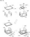
- FIG. 12 is a perspective view of a VCM and an IR filter according to an embodiment of the present invention
- FIG. 13 is a cross-sectional view of a ToF camera module including a VCM and an IR filter according to an embodiment of the present invention
- FIG. 14 is a diagram showing a process of coupling an IR filter and a magnet assembly included in a VCM according to an embodiment of the present invention
- FIG. 15 is a diagram showing a coupling process of a coil assembly included in a VCM according to an embodiment of the present invention
- FIG. 16 is a diagram showing a process of coupling a magnet assembly, an IR filter, and a coil assembly according to an embodiment of the present invention.
- the tilting unit 140 may include a VCM 1000, and the VCM 1000 may include a magnet assembly 1100 and a coil assembly 1200 and may be coupled to, brought into contact with, or connected to the IR filter 318.
- FIG. 13A for convenience of description, it is shown that the VCM 1000 is surrounded by the lens barrel 314 and the lens holder 318 and that the lens 312 and the IR filter 318 are omitted.
- the lens 312 and the IR filter 318 may be arranged as shown in FIG. 3 . That is, the lens 312 may be surrounded by the lens barrel 314 or may be accommodated in a space of the VCM 1000.
- the lens barrel 314 may be an element of the VCM 1000.
- the magnet assembly 1100 may include a magnet holder 1110 and a plurality of magnets 1120, and the plurality of magnets 1120 may be spaced apart on the magnet holder 1110 at predetermined intervals.
- the magnet holder 1110 may have a hollow circular ring shape or a quadrilateral ring shape, and a plurality of magnet guides 1112 may be formed to accommodate the plurality of magnets 1120.
- the magnet holder 1110 may contain a magnetic material or a soft magnetic material, e.g., Fe.
- the coil assembly 1200 may include a coil holder 1210, a plurality of coils 1220, and a coil terminal 1230, and the plurality of coils 1220 may be disposed on the coil holder 1210 and spaced apart from one another at predetermined intervals to make pairs with the plurality of magnets.
- the coil holder 1210 may have a hollow circular ring shape or a quadrilateral ring shape, and a plurality of coil guides 1212 may be formed to accommodate the plurality of coils 1220.
- the coil holder 1210 may be the lens barrel 314.
- the coil terminal 1230 may be connected to the plurality of coils 1220 and may apply power to the plurality of coils 1220.
- the IR filter 318 includes a glass layer holder 3182 and a glass layer 3184 supported by the glass layer holder 3182.
- the glass layer holder 3182 may include a first glass layer holder 3182-1 disposed under the glass layer 3184 and a second glass layer holder 3182-2 disposed on an upper edge of the glass layer 3184.
- the second glass layer holder 3182-2 may have a hollow circular ring shape or a quadrilateral ring shape and may be disposed in a hollow of the magnet holder 1110 and surrounded by the magnet holder 1110.
- the second glass layer holder 3182-2 may include a plurality of protrusions P1, P2, P3, and P4 corresponding to the plurality of magnet guides 1112 of the magnet holder 1110.
- the plurality of protrusions P1, P2, P3, and P4 may be moved such that the protrusions are brought into contact with or spaced apart from the plurality of magnet guides 1112.
- the second glass layer holder 3182-2 may contain a magnetic material or a soft magnetic material.
- an electric driving force may be generated between the plurality of magnet guides 1112 and the plurality of protrusions P1, P2, P3, and P4 of the second glass layer holder 3182-2, and the glass layer 3184 supported by the second glass layer holder 3182-2 may be tilted at a predetermined angle.
- a slope formed between the protrusion P1 and the protrusion P3 or a slope formed between the protrusion P2 and the protrusion P4 may vary depending on a force applied between the plurality of magnet guides 1112 and the plurality of protrusions P1, P2, P3, and P4.
- the slope of the glass layer 3184 may vary depending on the slope formed between the protrusion P1 and the protrusion P3 or the slope formed between the protrusion P2 and the protrusion P4.
- the slope of the IR filter 318, and particularly, the slope of the glass layer 3184 varies depending on the positions of the plurality of protrusions P1, P2, P3, and P4 of the second glass layer holder 3182-2. Accordingly, the second glass layer holder 3182-2 may be referred to herein as a shaper.
- a spacer 1130 may be further disposed between the magnet holder 1110 and the first glass layer holder 3182-1.
- the glass layer 3184 may be an IR-pass glass layer.
- the glass layer 3184 may be a general glass layer, and the IR filter 318 may further include an IR pass glass layer 3186 spaced apart from the glass layer 3184 and disposed on the image sensor 320.
- the IR pass glass layer 3186 is disposed on the image sensor 320, it is possible to reduce the possibility of moisture or foreign matter directly penetrating into the image sensor 320.
- the magnet assembly 1110 may further include a magnet holder 1140.
- the magnet holder 1140 may support upper portions of the plurality of magnets 1120, and thus the plurality of magnets 1120 may move more stably and reliably.
- the slope of the IR filter 318 may be controlled according to the driving of the VCM 1000.
- the IR filter 318 should be disposed together with the VCM 1000, and thus the IR filter 318 needs to be spaced apart from the image sensor 320.
- the slope of the IR filter 318 needs to be frequently changed, and thus a free space for the movement of the IR filter 318 is required.
- the possibility of moisture, foreign matter, and the like penetrating into the free space for the movement of the IR filter 318 increases, and thus the image sensor 320 may be easily exposed to moisture or foreign matter.
- a component for preventing the image sensor 320 from being exposed to moisture, foreign matter, and the like may be further included.
- FIG. 17 is a cross-sectional view of a portion of a camera module according to an embodiment of the present invention.
- an upper portion of the camera module e.g., the lens, the lens barrel, the VCM, and the like are omitted, but the description of FIGS. 3 and 10 to 14 may be equally applied.
- an image sensor 320 may be mounted on a printed circuit board 330 and accommodated in a housing 340.
- the housing may be a second lens holder 316-2.
- the slope of the IR filter 318 may be controlled by the VCM 1000 (see FIGS. 12 to 16 ). For example, when a first protrusion P1 of a first glass layer holder 3182-1 faces upward and the third protrusion P3 faces downward due to the driving of the VCM 1000, a glass layer 3184 of an IR filter 318 may be tilted.
- an elastic film 1400 may be disposed between the IR filter 318 and the image sensor 320.
- the elastic film 1400 may be fastened to the housing 340.
- one face of the elastic film 1400 may be fastened to the housing 340, and the other face of the elastic film 1400 may be coupled to the tilting unit 140.
- the elastic film 1400 may be, for example, a reverse osmosis (RO) membrane, a nano filtration (NF) membrane, an ultra-filtration (UF) membrane, a micro filtration (MF) membrane, or the like.
- RO reverse osmosis
- NF nano filtration
- UF ultra-filtration
- MF micro filtration
- the RO membrane is a membrane having a pore size of about 1 to 15 angstroms
- the NF membrane is a membrane having a pore size of about 10 angstroms
- the UF membrane is a membrane having a pore size of about 15 to 200 angstroms
- the MF membrane is a membrane having a pore size of about 200 to 1000 angstroms. Accordingly, it is possible to prevent moisture, foreign matter, and the like from penetrating into a space between the IR filter 318 and the housing 340, that is, the space arranged for the movement of the IR filter 318.
- the elastic film 1400 may be a transparent and stretchable film with a thickness of 25 to 50 ⁇ m, and the IR filter 318 may be disposed on the elastic film 1400 so that at least a portion of the IR filter 318 can be in direct contact with the elastic film 1400. That is, the shape of the elastic film 1400 may be controlled by the tilting unit 1400.
- the elastic film 1400 may be stretched or contracted together with the IR filter 318.
- the elastic film 1400 may be restored immediately along with the IR filter 318. Accordingly, it is possible to stably support the movement of the IR filter 318.
- FIGS. 18 to 23 show various examples of placing an elastic film.
- the elastic film 1400 may be adhered to the housing 340 for accommodating the image sensor 320 through an adhesive 1410.
- the elastic film 1400 may be fastened to the housing 340 for housing the image sensor 320 through an instrument 1420.
- the elastic film 1400 may be disposed to cover the outer circumferential surface of the housing 340 for accommodating the image sensor 320.
- an additional fastening member 1430 may be disposed to surround the outer circumferential surface of the housing 340.
- the elastic film 1400 may be disposed directly on the image sensor 320.
- the elastic film 1400 may be disposed between the first glass layer holder 3182-1 and the housing 340 and fastened by instructions 1440 and 1442.
- the elastic film 1400 may be adhered to the first glass layer holder 3182-1 and the housing 340 through adhesives 1450 and 1452.
- ToF camera module 110 lighting unit 120 : lens unit 130 : image sensor unit 140 : tilting unit 150 : image control unit
Landscapes
- Engineering & Computer Science (AREA)
- Physics & Mathematics (AREA)
- Multimedia (AREA)
- Signal Processing (AREA)
- General Physics & Mathematics (AREA)
- Optics & Photonics (AREA)
- Theoretical Computer Science (AREA)
- Electromagnetism (AREA)
- Computer Vision & Pattern Recognition (AREA)
- Health & Medical Sciences (AREA)
- Toxicology (AREA)
- Computing Systems (AREA)
- Studio Devices (AREA)
- Optical Radar Systems And Details Thereof (AREA)
Applications Claiming Priority (2)
| Application Number | Priority Date | Filing Date | Title |
|---|---|---|---|
| KR1020180043431A KR102473650B1 (ko) | 2018-04-13 | 2018-04-13 | 카메라 모듈 및 그의 깊이 정보 추출 방법 |
| PCT/KR2019/004416 WO2019199101A1 (fr) | 2018-04-13 | 2019-04-12 | Module appareil photo, et procédé d'extraction de carte de profondeur associé |
Publications (2)
| Publication Number | Publication Date |
|---|---|
| EP3780596A1 true EP3780596A1 (fr) | 2021-02-17 |
| EP3780596A4 EP3780596A4 (fr) | 2021-09-01 |
Family
ID=68164284
Family Applications (1)
| Application Number | Title | Priority Date | Filing Date |
|---|---|---|---|
| EP19784499.6A Pending EP3780596A4 (fr) | 2018-04-13 | 2019-04-12 | Module appareil photo, et procédé d'extraction de carte de profondeur associé |
Country Status (6)
| Country | Link |
|---|---|
| US (1) | US11568553B2 (fr) |
| EP (1) | EP3780596A4 (fr) |
| JP (1) | JP7485610B2 (fr) |
| KR (1) | KR102473650B1 (fr) |
| CN (1) | CN111971957B (fr) |
| WO (1) | WO2019199101A1 (fr) |
Cited By (1)
| Publication number | Priority date | Publication date | Assignee | Title |
|---|---|---|---|---|
| EP3758354A4 (fr) * | 2018-02-23 | 2021-04-14 | LG Innotek Co., Ltd. | Module de caméra et son procédé de traitement d'image à super-résolution |
Families Citing this family (5)
| Publication number | Priority date | Publication date | Assignee | Title |
|---|---|---|---|---|
| KR102513680B1 (ko) * | 2018-06-08 | 2023-03-24 | 엘지이노텍 주식회사 | 카메라 모듈 및 그의 깊이 정보 추출 방법 |
| KR102618276B1 (ko) * | 2019-01-07 | 2023-12-28 | 엘지이노텍 주식회사 | 카메라 모듈 |
| KR20210072458A (ko) * | 2019-12-09 | 2021-06-17 | 에스케이하이닉스 주식회사 | 비행시간거리측정 방식의 센싱 시스템 및 이미지 센서 |
| WO2021133054A1 (fr) * | 2019-12-26 | 2021-07-01 | 엘지이노텍 주식회사 | Module de caméra |
| US11867562B2 (en) * | 2022-01-25 | 2024-01-09 | Visera Technologies Company Limited | Optical devices |
Family Cites Families (15)
| Publication number | Priority date | Publication date | Assignee | Title |
|---|---|---|---|---|
| JP3038134B2 (ja) * | 1994-06-20 | 2000-05-08 | シャープ株式会社 | 撮像装置 |
| JPH0974524A (ja) * | 1995-07-05 | 1997-03-18 | Sharp Corp | 画像入力装置 |
| JPH09186920A (ja) * | 1995-12-27 | 1997-07-15 | Canon Inc | 画像入力装置 |
| JPH11187309A (ja) * | 1997-12-19 | 1999-07-09 | Canon Inc | 撮像装置及び撮像方法 |
| JP2005266676A (ja) | 2004-03-22 | 2005-09-29 | Nikon Corp | 可変光学ローパスフィルタおよび撮像ユニット |
| WO2007035720A2 (fr) | 2005-09-20 | 2007-03-29 | Deltasphere, Inc. | Procedes, systemes et produits informatiques permettant d'acquerir des informations de plages en 3d |
| US7566854B2 (en) * | 2006-12-08 | 2009-07-28 | Advanced Chip Engineering Technology Inc. | Image sensor module |
| US8629976B2 (en) * | 2007-10-02 | 2014-01-14 | Microsoft Corporation | Methods and systems for hierarchical de-aliasing time-of-flight (TOF) systems |
| JP2010122183A (ja) | 2008-11-21 | 2010-06-03 | Sanyo Electric Co Ltd | 物体検出装置および情報取得装置 |
| KR101925028B1 (ko) * | 2012-08-29 | 2018-12-04 | 엘지전자 주식회사 | 깊이 영상 생성 장치 및 방법 |
| CN103915454B (zh) * | 2012-12-31 | 2017-02-08 | 意法半导体研发(深圳)有限公司 | 具有对齐的ir滤光片和电介质层的图像传感器设备和相关方法 |
| KR20160142156A (ko) * | 2015-06-02 | 2016-12-12 | 주식회사 옵트론텍 | 오토 포커스 촬영 모듈을 이용한 광각 촬영 장치 |
| US9921298B2 (en) * | 2015-07-20 | 2018-03-20 | Google Llc | Method and apparatus for increasing the resolution of a time of flight pixel array |
| JP6852416B2 (ja) | 2016-03-10 | 2021-03-31 | 株式会社リコー | 距離測定装置、移動体、ロボット、装置及び3次元計測方法 |
| KR101804779B1 (ko) * | 2016-08-26 | 2017-12-05 | 엘지이노텍 주식회사 | 카메라 모듈 |
-
2018
- 2018-04-13 KR KR1020180043431A patent/KR102473650B1/ko active IP Right Grant
-
2019
- 2019-04-12 JP JP2020555858A patent/JP7485610B2/ja active Active
- 2019-04-12 EP EP19784499.6A patent/EP3780596A4/fr active Pending
- 2019-04-12 CN CN201980025629.2A patent/CN111971957B/zh active Active
- 2019-04-12 WO PCT/KR2019/004416 patent/WO2019199101A1/fr active Application Filing
- 2019-04-12 US US17/047,268 patent/US11568553B2/en active Active
Cited By (3)
| Publication number | Priority date | Publication date | Assignee | Title |
|---|---|---|---|---|
| EP3758354A4 (fr) * | 2018-02-23 | 2021-04-14 | LG Innotek Co., Ltd. | Module de caméra et son procédé de traitement d'image à super-résolution |
| US11425303B2 (en) | 2018-02-23 | 2022-08-23 | Lg Innotek Co., Ltd. | Camera module and super resolution image processing method thereof |
| US11770626B2 (en) | 2018-02-23 | 2023-09-26 | Lg Innotek Co., Ltd. | Camera module and super resolution image processing method thereof |
Also Published As
| Publication number | Publication date |
|---|---|
| KR20190119904A (ko) | 2019-10-23 |
| JP7485610B2 (ja) | 2024-05-16 |
| JP2021521438A (ja) | 2021-08-26 |
| US20210166408A1 (en) | 2021-06-03 |
| US11568553B2 (en) | 2023-01-31 |
| EP3780596A4 (fr) | 2021-09-01 |
| CN111971957B (zh) | 2024-03-08 |
| CN111971957A (zh) | 2020-11-20 |
| KR102473650B1 (ko) | 2022-12-02 |
| WO2019199101A1 (fr) | 2019-10-17 |
Similar Documents
| Publication | Publication Date | Title |
|---|---|---|
| EP3780596A1 (fr) | Module appareil photo, et procédé d'extraction de carte de profondeur associé | |
| CN112272948B (zh) | 相机模块及由此的深度信息提取方法 | |
| US11393112B2 (en) | Camera module and method for extracting depth information by same | |
| EP3907543A1 (fr) | Système optique et module de caméra le comprenant | |
| KR102571864B1 (ko) | 카메라 장치 | |
| CN112262572B (zh) | 相机模块及由此的深度信息获取方法 | |
| US11627301B2 (en) | Image sensor and camera module using same | |
| CN112771857B (zh) | 相机装置 | |
| US20210383561A1 (en) | Camera module | |
| CN113767621B (zh) | 相机模块 | |
| US11885884B2 (en) | Camera module | |
| US11867817B2 (en) | Camera module and depth information extraction method thereof | |
| KR20230027863A (ko) | 카메라 모듈 |
Legal Events
| Date | Code | Title | Description |
|---|---|---|---|
| STAA | Information on the status of an ep patent application or granted ep patent |
Free format text: STATUS: THE INTERNATIONAL PUBLICATION HAS BEEN MADE |
|
| PUAI | Public reference made under article 153(3) epc to a published international application that has entered the european phase |
Free format text: ORIGINAL CODE: 0009012 |
|
| STAA | Information on the status of an ep patent application or granted ep patent |
Free format text: STATUS: REQUEST FOR EXAMINATION WAS MADE |
|
| 17P | Request for examination filed |
Effective date: 20201105 |
|
| AK | Designated contracting states |
Kind code of ref document: A1 Designated state(s): AL AT BE BG CH CY CZ DE DK EE ES FI FR GB GR HR HU IE IS IT LI LT LU LV MC MK MT NL NO PL PT RO RS SE SI SK SM TR |
|
| AX | Request for extension of the european patent |
Extension state: BA ME |
|
| RIC1 | Information provided on ipc code assigned before grant |
Ipc: H04N 13/207 20180101AFI20210409BHEP Ipc: H04N 13/254 20180101ALI20210409BHEP Ipc: H04N 13/106 20180101ALI20210409BHEP Ipc: H04N 5/232 20060101ALI20210409BHEP Ipc: H04N 5/225 20060101ALI20210409BHEP |
|
| DAV | Request for validation of the european patent (deleted) | ||
| DAX | Request for extension of the european patent (deleted) | ||
| A4 | Supplementary search report drawn up and despatched |
Effective date: 20210730 |
|
| RIC1 | Information provided on ipc code assigned before grant |
Ipc: H04N 13/207 20180101AFI20210726BHEP Ipc: H04N 13/254 20180101ALI20210726BHEP Ipc: H04N 13/106 20180101ALI20210726BHEP Ipc: H04N 5/232 20060101ALI20210726BHEP Ipc: H04N 5/225 20060101ALI20210726BHEP |
|
| STAA | Information on the status of an ep patent application or granted ep patent |
Free format text: STATUS: EXAMINATION IS IN PROGRESS |
|
| 17Q | First examination report despatched |
Effective date: 20230811 |