EP3780071A1 - Semiconductor device and method for manufacturing same - Google Patents
Semiconductor device and method for manufacturing same Download PDFInfo
- Publication number
- EP3780071A1 EP3780071A1 EP18912862.2A EP18912862A EP3780071A1 EP 3780071 A1 EP3780071 A1 EP 3780071A1 EP 18912862 A EP18912862 A EP 18912862A EP 3780071 A1 EP3780071 A1 EP 3780071A1
- Authority
- EP
- European Patent Office
- Prior art keywords
- region
- groove
- semiconductor
- sidewall
- conductivity type
- Prior art date
- Legal status (The legal status is an assumption and is not a legal conclusion. Google has not performed a legal analysis and makes no representation as to the accuracy of the status listed.)
- Granted
Links
Images





Classifications
-
- H—ELECTRICITY
- H10—SEMICONDUCTOR DEVICES; ELECTRIC SOLID-STATE DEVICES NOT OTHERWISE PROVIDED FOR
- H10D—INORGANIC ELECTRIC SEMICONDUCTOR DEVICES
- H10D30/00—Field-effect transistors [FET]
- H10D30/60—Insulated-gate field-effect transistors [IGFET]
- H10D30/64—Double-diffused metal-oxide semiconductor [DMOS] FETs
- H10D30/66—Vertical DMOS [VDMOS] FETs
- H10D30/668—Vertical DMOS [VDMOS] FETs having trench gate electrodes, e.g. UMOS transistors
-
- H—ELECTRICITY
- H10—SEMICONDUCTOR DEVICES; ELECTRIC SOLID-STATE DEVICES NOT OTHERWISE PROVIDED FOR
- H10D—INORGANIC ELECTRIC SEMICONDUCTOR DEVICES
- H10D12/00—Bipolar devices controlled by the field effect, e.g. insulated-gate bipolar transistors [IGBT]
- H10D12/01—Manufacture or treatment
- H10D12/031—Manufacture or treatment of IGBTs
-
- H—ELECTRICITY
- H10—SEMICONDUCTOR DEVICES; ELECTRIC SOLID-STATE DEVICES NOT OTHERWISE PROVIDED FOR
- H10D—INORGANIC ELECTRIC SEMICONDUCTOR DEVICES
- H10D30/00—Field-effect transistors [FET]
- H10D30/01—Manufacture or treatment
- H10D30/021—Manufacture or treatment of FETs having insulated gates [IGFET]
- H10D30/028—Manufacture or treatment of FETs having insulated gates [IGFET] of double-diffused metal oxide semiconductor [DMOS] FETs
- H10D30/0291—Manufacture or treatment of FETs having insulated gates [IGFET] of double-diffused metal oxide semiconductor [DMOS] FETs of vertical DMOS [VDMOS] FETs
-
- H—ELECTRICITY
- H10—SEMICONDUCTOR DEVICES; ELECTRIC SOLID-STATE DEVICES NOT OTHERWISE PROVIDED FOR
- H10D—INORGANIC ELECTRIC SEMICONDUCTOR DEVICES
- H10D30/00—Field-effect transistors [FET]
- H10D30/60—Insulated-gate field-effect transistors [IGFET]
- H10D30/64—Double-diffused metal-oxide semiconductor [DMOS] FETs
- H10D30/65—Lateral DMOS [LDMOS] FETs
- H10D30/658—Lateral DMOS [LDMOS] FETs having trench gate electrodes
-
- H—ELECTRICITY
- H10—SEMICONDUCTOR DEVICES; ELECTRIC SOLID-STATE DEVICES NOT OTHERWISE PROVIDED FOR
- H10D—INORGANIC ELECTRIC SEMICONDUCTOR DEVICES
- H10D62/00—Semiconductor bodies, or regions thereof, of devices having potential barriers
- H10D62/10—Shapes, relative sizes or dispositions of the regions of the semiconductor bodies; Shapes of the semiconductor bodies
- H10D62/102—Constructional design considerations for preventing surface leakage or controlling electric field concentration
- H10D62/103—Constructional design considerations for preventing surface leakage or controlling electric field concentration for increasing or controlling the breakdown voltage of reverse-biased devices
- H10D62/105—Constructional design considerations for preventing surface leakage or controlling electric field concentration for increasing or controlling the breakdown voltage of reverse-biased devices by having particular doping profiles, shapes or arrangements of PN junctions; by having supplementary regions, e.g. junction termination extension [JTE]
- H10D62/109—Reduced surface field [RESURF] PN junction structures
- H10D62/111—Multiple RESURF structures, e.g. double RESURF or 3D-RESURF structures
-
- H—ELECTRICITY
- H10—SEMICONDUCTOR DEVICES; ELECTRIC SOLID-STATE DEVICES NOT OTHERWISE PROVIDED FOR
- H10D—INORGANIC ELECTRIC SEMICONDUCTOR DEVICES
- H10D62/00—Semiconductor bodies, or regions thereof, of devices having potential barriers
- H10D62/10—Shapes, relative sizes or dispositions of the regions of the semiconductor bodies; Shapes of the semiconductor bodies
- H10D62/13—Semiconductor regions connected to electrodes carrying current to be rectified, amplified or switched, e.g. source or drain regions
- H10D62/149—Source or drain regions of field-effect devices
- H10D62/151—Source or drain regions of field-effect devices of IGFETs
- H10D62/156—Drain regions of DMOS transistors
- H10D62/158—Dispositions
-
- H—ELECTRICITY
- H10—SEMICONDUCTOR DEVICES; ELECTRIC SOLID-STATE DEVICES NOT OTHERWISE PROVIDED FOR
- H10D—INORGANIC ELECTRIC SEMICONDUCTOR DEVICES
- H10D62/00—Semiconductor bodies, or regions thereof, of devices having potential barriers
- H10D62/80—Semiconductor bodies, or regions thereof, of devices having potential barriers characterised by the materials
- H10D62/83—Semiconductor bodies, or regions thereof, of devices having potential barriers characterised by the materials being Group IV materials, e.g. B-doped Si or undoped Ge
- H10D62/832—Semiconductor bodies, or regions thereof, of devices having potential barriers characterised by the materials being Group IV materials, e.g. B-doped Si or undoped Ge being Group IV materials comprising two or more elements, e.g. SiGe
- H10D62/8325—Silicon carbide
-
- H—ELECTRICITY
- H10—SEMICONDUCTOR DEVICES; ELECTRIC SOLID-STATE DEVICES NOT OTHERWISE PROVIDED FOR
- H10D—INORGANIC ELECTRIC SEMICONDUCTOR DEVICES
- H10D64/00—Electrodes of devices having potential barriers
- H10D64/20—Electrodes characterised by their shapes, relative sizes or dispositions
- H10D64/23—Electrodes carrying the current to be rectified, amplified, oscillated or switched, e.g. sources, drains, anodes or cathodes
- H10D64/251—Source or drain electrodes for field-effect devices
- H10D64/256—Source or drain electrodes for field-effect devices for lateral devices wherein the source or drain electrodes are recessed in semiconductor bodies
-
- H—ELECTRICITY
- H10—SEMICONDUCTOR DEVICES; ELECTRIC SOLID-STATE DEVICES NOT OTHERWISE PROVIDED FOR
- H10D—INORGANIC ELECTRIC SEMICONDUCTOR DEVICES
- H10D30/00—Field-effect transistors [FET]
- H10D30/01—Manufacture or treatment
- H10D30/021—Manufacture or treatment of FETs having insulated gates [IGFET]
- H10D30/028—Manufacture or treatment of FETs having insulated gates [IGFET] of double-diffused metal oxide semiconductor [DMOS] FETs
- H10D30/0281—Manufacture or treatment of FETs having insulated gates [IGFET] of double-diffused metal oxide semiconductor [DMOS] FETs of lateral DMOS [LDMOS] FETs
- H10D30/0289—Manufacture or treatment of FETs having insulated gates [IGFET] of double-diffused metal oxide semiconductor [DMOS] FETs of lateral DMOS [LDMOS] FETs using recessing of the gate electrodes, e.g. to form trench gate electrodes
-
- H—ELECTRICITY
- H10—SEMICONDUCTOR DEVICES; ELECTRIC SOLID-STATE DEVICES NOT OTHERWISE PROVIDED FOR
- H10D—INORGANIC ELECTRIC SEMICONDUCTOR DEVICES
- H10D30/00—Field-effect transistors [FET]
- H10D30/60—Insulated-gate field-effect transistors [IGFET]
- H10D30/64—Double-diffused metal-oxide semiconductor [DMOS] FETs
- H10D30/65—Lateral DMOS [LDMOS] FETs
- H10D30/657—Lateral DMOS [LDMOS] FETs having substrates comprising insulating layers, e.g. SOI-LDMOS transistors
-
- H—ELECTRICITY
- H10—SEMICONDUCTOR DEVICES; ELECTRIC SOLID-STATE DEVICES NOT OTHERWISE PROVIDED FOR
- H10D—INORGANIC ELECTRIC SEMICONDUCTOR DEVICES
- H10D62/00—Semiconductor bodies, or regions thereof, of devices having potential barriers
- H10D62/10—Shapes, relative sizes or dispositions of the regions of the semiconductor bodies; Shapes of the semiconductor bodies
- H10D62/113—Isolations within a component, i.e. internal isolations
- H10D62/115—Dielectric isolations, e.g. air gaps
- H10D62/116—Dielectric isolations, e.g. air gaps adjoining the input or output regions of field-effect devices, e.g. adjoining source or drain regions
-
- H—ELECTRICITY
- H10—SEMICONDUCTOR DEVICES; ELECTRIC SOLID-STATE DEVICES NOT OTHERWISE PROVIDED FOR
- H10D—INORGANIC ELECTRIC SEMICONDUCTOR DEVICES
- H10D62/00—Semiconductor bodies, or regions thereof, of devices having potential barriers
- H10D62/80—Semiconductor bodies, or regions thereof, of devices having potential barriers characterised by the materials
- H10D62/85—Semiconductor bodies, or regions thereof, of devices having potential barriers characterised by the materials being Group III-V materials, e.g. GaAs
- H10D62/8503—Nitride Group III-V materials, e.g. AlN or GaN
-
- H—ELECTRICITY
- H10—SEMICONDUCTOR DEVICES; ELECTRIC SOLID-STATE DEVICES NOT OTHERWISE PROVIDED FOR
- H10D—INORGANIC ELECTRIC SEMICONDUCTOR DEVICES
- H10D64/00—Electrodes of devices having potential barriers
- H10D64/01—Manufacture or treatment
- H10D64/013—Manufacture or treatment of electrodes having a conductor capacitively coupled to a semiconductor by an insulator
- H10D64/01302—Manufacture or treatment of electrodes having a conductor capacitively coupled to a semiconductor by an insulator the insulator being formed after the semiconductor body, the semiconductor being silicon
- H10D64/01332—Making the insulator
- H10D64/01336—Making the insulator on single crystalline silicon, e.g. chemical oxidation using a liquid
- H10D64/0134—Making the insulator on single crystalline silicon, e.g. chemical oxidation using a liquid with a treatment, e.g. annealing, after the formation of the insulator and before the formation of the conductor
-
- H—ELECTRICITY
- H10—SEMICONDUCTOR DEVICES; ELECTRIC SOLID-STATE DEVICES NOT OTHERWISE PROVIDED FOR
- H10D—INORGANIC ELECTRIC SEMICONDUCTOR DEVICES
- H10D64/00—Electrodes of devices having potential barriers
- H10D64/01—Manufacture or treatment
- H10D64/013—Manufacture or treatment of electrodes having a conductor capacitively coupled to a semiconductor by an insulator
- H10D64/01302—Manufacture or treatment of electrodes having a conductor capacitively coupled to a semiconductor by an insulator the insulator being formed after the semiconductor body, the semiconductor being silicon
- H10D64/01332—Making the insulator
- H10D64/01336—Making the insulator on single crystalline silicon, e.g. chemical oxidation using a liquid
- H10D64/01344—Making the insulator on single crystalline silicon, e.g. chemical oxidation using a liquid in a nitrogen-containing ambient, e.g. N2O oxidation
-
- H—ELECTRICITY
- H10—SEMICONDUCTOR DEVICES; ELECTRIC SOLID-STATE DEVICES NOT OTHERWISE PROVIDED FOR
- H10D—INORGANIC ELECTRIC SEMICONDUCTOR DEVICES
- H10D64/00—Electrodes of devices having potential barriers
- H10D64/01—Manufacture or treatment
- H10D64/013—Manufacture or treatment of electrodes having a conductor capacitively coupled to a semiconductor by an insulator
- H10D64/01302—Manufacture or treatment of electrodes having a conductor capacitively coupled to a semiconductor by an insulator the insulator being formed after the semiconductor body, the semiconductor being silicon
- H10D64/01332—Making the insulator
- H10D64/01336—Making the insulator on single crystalline silicon, e.g. chemical oxidation using a liquid
- H10D64/01346—Making the insulator on single crystalline silicon, e.g. chemical oxidation using a liquid in a gaseous ambient using an oxygen or a water vapour, e.g. oxidation through a layer
-
- H—ELECTRICITY
- H10—SEMICONDUCTOR DEVICES; ELECTRIC SOLID-STATE DEVICES NOT OTHERWISE PROVIDED FOR
- H10P—GENERIC PROCESSES OR APPARATUS FOR THE MANUFACTURE OR TREATMENT OF DEVICES COVERED BY CLASS H10
- H10P30/00—Ion implantation into wafers, substrates or parts of devices
- H10P30/20—Ion implantation into wafers, substrates or parts of devices into semiconductor materials, e.g. for doping
- H10P30/22—Ion implantation into wafers, substrates or parts of devices into semiconductor materials, e.g. for doping using masks
- H10P30/221—Ion implantation into wafers, substrates or parts of devices into semiconductor materials, e.g. for doping using masks characterised by the angle between the ion beam and the mask
-
- H—ELECTRICITY
- H10—SEMICONDUCTOR DEVICES; ELECTRIC SOLID-STATE DEVICES NOT OTHERWISE PROVIDED FOR
- H10P—GENERIC PROCESSES OR APPARATUS FOR THE MANUFACTURE OR TREATMENT OF DEVICES COVERED BY CLASS H10
- H10P30/00—Ion implantation into wafers, substrates or parts of devices
- H10P30/20—Ion implantation into wafers, substrates or parts of devices into semiconductor materials, e.g. for doping
- H10P30/222—Ion implantation into wafers, substrates or parts of devices into semiconductor materials, e.g. for doping characterised by the angle between the ion beam and the crystal planes or the main crystal surface
Definitions
- the present invention relates to semiconductor devices and methods for manufacturing the same.
- a semiconductor device in which in order to improve the trade-off characteristic between breakdown voltage and on-resistance by decreasing the dimensions of the unit cell, a drain region is formed at the bottom part of a trench formed at a part of the surface layer of a semiconductor substrate, and a sidewall of the trench is a drift region (see Patent Literature 1).
- This semiconductor device has a drain electrode on a conducting material filling the inside of the trench. Then, a base region and a source region are formed in part of the surface layer of the semiconductor substrate where the trench is not formed, and the drain region and the source region are disposed on the respective sides of the gate electrode.
- Patent Literature 1 Japanese Patent Application Publication No. H08-181313
- the region immediately below the source region does not contribute to the operation of the transistor. This raises a problem that the chip area of the transistor is not used effectively, requiring an extra area accordingly.
- the present invention has been made in light of the above problem, and an object thereof is to provide a semiconductor device and method of manufacturing the same that make it possible to reduce the chip area of a transistor.
- a summary of a semiconductor device is that the semiconductor device includes: a drift region disposed at the bottom part of a groove formed on a substrate; a well region and source region layered in a sidewall of the groove; and a drain region disposed in the groove, and a gate electrode is disposed in a gate trench that has an opening extending over the upper surfaces of the well region and the source region and extends in the depth direction of the groove.
- a summary of a method of manufacturing a semiconductor device is that the method includes the steps of: forming a drift region at the bottom part of a groove formed in a substrate; forming a well region and source region layered in a sidewall of the groove; and forming a drain region in the groove, and a gate electrode is formed in a gate trench that has an opening extending over the upper surfaces of the well region and the source region and extends in the depth direction of the groove.
- the present invention provides a semiconductor device and method of manufacturing the same that make it possible to reduce the chip area of a transistor.
- a semiconductor device includes, as illustrated in Fig. 1 , a substrate 10 having a groove 100 formed on its main surface, and a drift region 20, well region 30, first semiconductor region 40, and second semiconductor region 50 formed on the substrate 10.
- the drift region 20 is of a first conductivity type and has a portion disposed at a bottom part of the groove 100. Note that in the embodiment illustrated in Fig. 1 , the drift region 20 is disposed to continue from one sidewall of the groove 100 (hereinafter referred to as the "first sidewall") to the bottom part of the groove 100.
- the well region 30 which is of a second conductivity type is disposed in the first sidewall of the groove 100 to be connected to the drift region 20.
- the well region 30 illustrated in Fig. 1 is disposed on the surface of the drift region 20 in the first sidewall of the groove 100, and the lower end of the well region 30 is connected to the drift region 20 at the bottom part of the groove 100.
- the first semiconductor region 40 which is of the first conductivity type is disposed on the surface of the well region 30 in the first sidewall of the groove 100.
- the first semiconductor region 40 is disposed on the surface of the well region 30 not to extend over the outer edge of the well region 30 so that the first semiconductor region 40 is isolated from the drift region 20. Accordingly, as illustrated in Fig. 1 , the lower end of the first semiconductor region 40 is positioned above the lower end of the well region 30.
- the second semiconductor region 50 which is of the first conductivity type is disposed in the groove 100 to be opposed to the well region 30 via the drift region 20.
- the second semiconductor region 50 is connected to the drift region 20 at a position away from the well region 30.
- the second semiconductor region 50 illustrated in Fig. 2 is disposed at the bottom part of the groove 100 to adjoin to the drift region 20 to be close to the sidewall of the groove 100 opposed to the first sidewall (hereinafter referred to as the "second sidewall").
- first conductivity type and the second conductivity type are conductivity types opposite to each other. Specifically, if the first conductivity type is n-type, then the second conductivity type is p-type. If the first conductivity type is p-type, then the second conductivity type is n-type. In the following, description is made as an example for the case where the first conductivity type is n-type and the second conductivity type is p-type.
- the semiconductor device illustrated in Fig. 1 has, in the first sidewall of the groove 100, the drift region 20, the well region 30, and the first semiconductor region 40, and those are layered along the direction of the normal line to the first sidewall (hereinafter referred to as the "lateral direction" of the groove 100). Then, openings are formed to extend over the upper surfaces of the drift region 20, the well region 30, and the first semiconductor region 40, and from the openings, multiple gate trenches are formed to extend in the depth direction of the groove 100.
- the gate trenches have a gate insulating film 65 disposed on their inner wall surfaces. The gate trenches are formed to reach the drift region 20 disposed at the bottom part of the groove 100.
- the gate insulating film 65 is formed continuously over the drift region 20, the well region 30, and the first semiconductor region 40 in the lateral direction. Inside the gate trench, a gate electrode 60 is disposed to be opposed to the well region 30 via the gate insulating film 65.
- the semiconductor device illustrated in Fig. 1 also includes a first main electrode 70 electrically connected to the first semiconductor region 40 and a second main electrode 80 electrically connected to the second semiconductor region 50.
- the first main electrode 70 is disposed on the surface of the first semiconductor region 40 in the first sidewall of the groove 100.
- the second main electrode 80 is disposed in the second sidewall of the groove 100 to be opposed to the first main electrode 70, and the lower end of the second main electrode 80 is in contact with the second semiconductor region 50 at the bottom part of the groove 100.
- the first main electrode 70 is one end of the current route of the main electrical current that flows through the semiconductor device in the on state.
- the second main electrode 80 is the other end of the current route.
- the main electrical current of the semiconductor device flows between the first main electrode 70 and the second main electrode 80 via the first semiconductor region 40, the well region 30, the drift region 20, and the second semiconductor region 50.
- the semiconductor device illustrated in Fig. 1 works as a transistor, and the main electrical current is controlled by applying a specified voltage to the gate electrodes 60 disposed in a middle of the current route.
- the semiconductor device is described based on the assumption that the first semiconductor region 40 is the source region, the first main electrode 70 is the source electrode, the second semiconductor region 50 is the drain region, and the second main electrode 80 is the drain electrode.
- the groove 100 is filled with an isolation insulating film 90.
- the isolation insulating film 90 is disposed above the drift region 20 disposed at the bottom part of the groove 100 and between the source electrode 70 and the drain electrode 80.
- This isolation insulating film 90 insulates and isolates the drift region 20 and the source electrode 70 disposed above the drift region 20 from each other.
- Fig. 1 illustrates the semiconductor device as if the isolation insulating film 90 were transparent to make it easy to understand the structure of the semiconductor device. In other words, only the outer edges are depicted for the isolation insulating film 90 (the same is true of other perspective diagrams).
- the regions outside the groove 100 are regions of the substrate 10 where the groove 100 is not formed.
- the portion of the drift region 20 disposed at the bottom part of the groove 100, illustrated in Fig. 1 has a structure in which an n-type drift region 21, which is a first conductivity type region, and a p-type drift region 22, which is a second conductivity type region, are disposed alternately in parallel with the main surface of the substrate 10 and along the direction in which the groove 100 extends.
- the semiconductor device illustrated in Fig. 1 has a super junction structure (SJ structure) in which multiple pn junctions are arranged at a constant cycle along the direction in which the groove 100 extends (hereinafter referred to as the "longitudinal direction" of the groove 100).
- the main electrical current flows through the n-type drift regions 21 in which the concentration of n-type impurities is high in the drift region 20, and this reduces the on-resistance.
- the n-type drift regions 21 and the p-type drift regions 22 are depleted by depletion layers spreading from pn junctions, keeping high breakdown voltage.
- channel regions are formed in the on state in the well region 30 which is in contact with the gate insulating films 65.
- the basic operation of the semiconductor device illustrated in Fig. 1 will be described.
- the semiconductor device functions as a transistor by the potential of the gate electrodes 60 being controlled with respect to the potential of the source electrode 70 in the state where a positive voltage is applied to the drain electrode 80.
- the voltage between the gate electrodes 60 and the source electrode 70 is a specified threshold voltage or higher, the inversion layers are formed in the channel regions in the well region 30 on the side surfaces of the gate electrodes 60.
- the main electrical current flows between the drain electrode 80 and the source electrode 70.
- the main electrical current flows in the well region 30 along the direction in parallel with the main surface of the substrate 10.
- the arrow I indicates the current route of the main electrical current of the semiconductor device in the on state.
- the voltage between the gate electrodes 60 and the source electrode 70 is set to a specified threshold voltage or lower. This makes the inversion layers disappear, cutting off the main electrical current.
- depletion layers spread from the pn junction between the well region 30 and the drift region 20 toward the drain region 50.
- depletion layers 200 spread from the interfaces between the n-type drift regions 21 and the p-type drift regions 22.
- both the n-type drift regions 21 and the p-type drift regions 22 are completely depleted (which is called the pinch-off state).
- the electric field distribution of the n-type drift region 21 and the p-type drift region 22 becomes a uniform rectangle distribution, which greatly decreases the maximum electric field exerted on the semiconductor device. This improves the breakdown voltage of the semiconductor device.
- the source region 40 and the source electrode 70 are disposed above the drift region 20 disposed at the bottom part of the groove 100.
- the region immediately below the source electrode 70 is an active region, which is not a region that does not contributes to the operation of the transistor.
- a region that does not contribute to the operation of the transistor is reduced, which makes it possible to reduce the chip area.
- the source region 40 and the well region 30 are disposed in the first sidewall of the groove 100, and the gate trenches are formed to extend in the depth direction of the groove 100.
- the end portion of the channel region extends in the depth direction along the first sidewall of the groove 100.
- the channel region is formed to have a gate width of from the opening of the groove 100 to the bottom part of the groove 100. The wide channel region formed as described above reduces the on-resistance.
- the source region 40 is formed in the groove 100 along the first sidewall, and the source region 40 extends in the depth direction of the groove 100. This allows the contact portion between the source region 40 and the source electrode 70 formed along the first sidewall of the groove 100 to extend in the depth direction of the groove 100.
- This configuration makes it possible to increase the contact area without increasing the chip area, compared to the case of forming the contact portion between the source region 40 and the source electrode 70 to be in parallel with the main surface of the substrate 10.
- the contact resistance between the source region 40 and the source electrode 70 is reduced, which in turn reduces the on-resistance.
- the semiconductor device illustrated in Fig. 1 has a structure in which part of the drift region 20 is disposed in the first sidewall of the groove 100.
- the well region 30 opposed to the gate insulating films 65 induces channel charge, and the semiconductor device is turned to the on state, accumulated charge is generated at the boundary between the drift region 20 and the gate insulating film 65 in the region surrounded by the dashed line A in Fig. 4 .
- the current route caused by this accumulated charge is formed in parallel with the channel regions formed in the well region 30, providing the effect of reducing resistance components in the channel regions of the semiconductor device.
- the substrate 10 be an insulating substrate.
- an insulating substrate is not necessary between the substrate 10 and the cooling unit.
- a substrate "having an insulating property" means that the resistivity of the substrate is several k ⁇ cm or more.
- silicon carbide having an insulating property is used for the substrate 10.
- SiC silicon carbide
- polytypes crystal polymorphs
- 4H-SiC substrate can be used for the substrate 10.
- SiC substrate for the substrate 10 provides a higher insulating property and a higher thermal conductivity of the substrate 10. This allows the semiconductor device to be cooled efficiently by attaching the back surface of the substrate 10 directly to a cooling mechanism. Since this structure provides a larger thermal conductivity in the SiC substrate, heat generation caused by the main electrical current when the semiconductor device is in the on state can be dissipated efficiency.
- SiC is a wide band gap semiconductor, in which the number of intrinsic carriers is small, and hence, it is easy to achieve a higher insulating property, and use of SiC makes it possible to achieve a semiconductor device with a high breakdown voltage.
- a groove 100 is formed on the main surface of a substrate 10 which is non-doped silicon carbide insulating semiconductor.
- the depth of the groove 100 is, for example, approximately 10 to 20 ⁇ m, and the width in in the lateral direction is, for example, approximately 10 ⁇ m.
- a mask material 111 is formed in a specified shape on the main surface of the substrate 10 (see Fig. 5 ).
- the mask material 111 may be, for example, a silicon oxide film, and the deposition method may be a thermal CVD method or a plasma CVD method.
- a photoresist material on the mask material 111 is patterned (not illustrated).
- a general photolithography technique is used for the patterning method.
- the patterned photoresist material is used as a mask to etch the mask material 111.
- a wet etching method using hydrofluoric acid or a dry etching method such as reactive ion etching is used.
- the photoresist material is removed using oxygen plasma, sulfuric acid, or the like.
- the mask material 111 formed as described above is used as an etching mask to selectively etch substrate 10 by a dry etching method.
- the groove 100 is formed as illustrated in Fig. 5 .
- a portion of the drift region 20 that is along the first sidewall 11 of the groove 100 (hereinafter referred to as a "sidewall portion" of the drift region 20) is formed by ion implantation or the like.
- the sidewall portion of the drift region 20 is formed by ion-implanting impurities of a first conductivity type obliquely from above the opening of the groove 100 into the first sidewall.
- the impurities can be implanted only into the first sidewall of the groove 100 by setting the angle at which the impurities are implanted into the first sidewall of the groove 100, according to the aspect ratio determined from the depth and the width in in the lateral direction of the groove 100.
- the sidewall portion of the drift region 20 is formed in the first sidewall of the groove 100. Since the impurities are implanted from obliquely above, the lower end of the sidewall portion of the drift region 20 reaches below the bottom part of the groove 100.
- the n-type drift regions 21 are formed in the portion of the drift region 20 disposed at the bottom part of the groove 100 (hereinafter referred to as the "bottom portion" of the drift region 20).
- a mask material 112 through which the regions of the bottom part of the groove 100 to be the n-type drift regions 21 are exposed is formed by a photolithography technique.
- the n-type drift regions 21 are formed selectively above the substrate 10 by ion-implanting impurities of the first conductivity type using the mask material 112 as a mask.
- the impurities are implanted a little obliquely toward the first sidewall from the direction of the normal line to the main surface of the substrate 10, and thus, the impurities are implanted into portions below the sidewall portion of the drift region 20.
- the sidewall portion and bottom portion of the drift region 20 are connected to each other. After that, the mask material 112 is removed.
- a well region 30 is formed in the first sidewall of the groove 100 to be connected to the drift region 20 by ion implantation or the like.
- the well region 30 is formed to cover the sidewall portion of the drift region 20 by ion-implanting impurities of a second conductivity type obliquely from above the opening of the groove 100 into the first sidewall.
- the impurities can be implanted only into the first sidewall of the groove 100 by setting the angle at which the impurities are implanted into the first sidewall of the groove 100, according to the aspect ratio determined from the depth and the width in in the lateral direction of the groove 100.
- the well region 30 is formed in the first sidewall of the groove 100.
- the impurity concentration of the well region 30 is, for example, approximately 1E15/cm 3 to 1E19/cm 3 .
- the p-type drift regions 22 are formed in the bottom portion of the drift region 20.
- a mask material 113 through which the regions of the bottom part of the groove 100 to be the p-type drift regions 22 are exposed is formed, and then, the p-type drift regions 22 are formed selectively above the substrate 10 by ion-implanting impurities of the second conductivity type using the mask material 113 used as a mask.
- the bottom portion of the drift region 20 is formed in which the n-type drift region and the p-type drift region are disposed alternately along the longitudinal direction of the groove 100. After that, the mask material 113 is removed.
- N nitrogen
- Al aluminum
- B boron
- the ratio of the total amount of p-type impurities in the p-type drift region and the total amount of n-type impurities in the n-type drift region needs to be set to around 1.
- Nd representing the concentration of n-type impurities in the n-type drift region 21
- Na representing the concentration of p-type impurities in the p-type drift region 22
- Wn representing the width of the n-type drift region 21
- Width Wn and width Wp are the widths in the direction in which the n-type drift region 21 and the p-type drift region 22 are repeatedly arranged.
- the impurity concentrations of the n-type drift region 21 and the p-type drift region are set to satisfy equation (1).
- the n-type drift regions 21 and the p-type drift regions 22 are depleted in the off state, which increases the breakdown voltage per unit area of the drift region 20.
- the impurity concentration of the drift region 20 is, for example, approximately 1E15/cm 3 to 1E19/cm 3 .
- a source region 40 is formed on the surface of the well region 30 in the first sidewall of the groove 100.
- the source region 40 is formed in the region in which the well region 30 has been formed by ion-implanting impurities of the first conductivity type obliquely from above the opening of the groove 100 into the first sidewall.
- the impurities are implanted only into the well region 30 of the groove 100 by setting the angle at which the impurities are implanted into the first sidewall of the groove 100, according to the aspect ratio determined from the depth and the width in in the lateral direction of the groove 100.
- the impurity concentration of the source region 40 is, for example, approximately 1E18/cm 3 to 1E21/cm 3 .
- the source region 40 is formed to be away from the drift region 20. Accordingly, the impurity implantation angle of ion implantation to form the source region 40 is set shallower than the impurity implantation angle of ion implantation to form the well region 30. From this setting, the lower end of the source region 40 is positioned above the lower end of the well region 30, which prevents the source region 40 from extending over to the outside of the well region 30.
- a drain region 50 is formed in the groove 100 to be opposed to the well region 30 via the drift region 20.
- the drain region 50 is connected to the drift region 20 at a position away from the well region 30.
- the drain region 50 is formed selectively at the bottom part of the groove 100 by ion-implanting impurities of the first conductivity type using, as a mask, a mask material 114 formed such that a specified region is exposed through the mask material 114 as illustrated in Fig. 11 .
- the impurity concentration of the drain region 50 is, for example, approximately 1E18/cm 3 to 1E21/cm 3 .
- the ion-implanted impurities are activated by heat treatment.
- heat treatment at around 1700°C is performed in argon atmosphere or nitrogen atmosphere.
- openings are formed to extend over the upper surfaces of the sidewall portion of the drift region 20, the well region 30, and the source region 40, and gate trenches 600 are formed to extend in the depth direction of the groove 100.
- a mask material formed on the upper surface of the substrate 10 is patterned by a photolithography technique, and then, the gate trenches 600 are formed by etching.
- the gate trenches 600 are formed to have a width to reach the sidewall portion of the drift region 20, the well region 30, and the source region 40 and a depth to reach the drift region 20.
- gate insulating films 65 are formed on the inner wall surfaces of the gate trenches 600.
- the inner wall surfaces of the gate trenches 600 are oxidized to form the gate insulating films 65.
- the method of forming the gate insulating films 65 may be a thermal oxidization method or a deposition method.
- the substrate 10 is heated to a temperature at around 1100°C in oxygen atmosphere.
- annealing at around 1000°C may be performed in the atmosphere of nitrogen, argon, N 2 O, or the like to decrease the interface state at the interface between the well region 30 and the gate insulating films 65.
- thermal oxidation in NO or N 2 O atmosphere may be performed really. In that case, a temperature around 1100 to 1400°C is preferable.
- the thickness of the gate insulating film 65 is approximately several tens nm.
- the gate electrodes 60 are formed inside the gate trenches 600.
- the gate electrode 60 is opposed to the well region 30 via the gate insulating film 65. Because a typical material of the gate electrode 60 is polysilicon films, here description is made of the case of using polysilicon films for the gate electrodes 60.
- the deposition method of the polysilicon films may be a low-pressure CVD method or the like.
- the thickness of a deposited polysilicon film is set to a value larger than half the width in the longitudinal direction of the opening of the gate trench 600. Since a polysilicon film is formed from the inner wall surfaces of the gate trench 600, the gate trench 600 can be completely filled with a polysilicon film by setting the thickness of the polysilicon film as described above. For example, in the case where the width of the gate trench 600 is 2 ⁇ m, a polysilicon film is formed such that the film thickness is 1 ⁇ m or more. After the polysilicon film is deposited, an annealing treatment at 950°C is performed in phosphorus oxychloride POCl 3 to form an n-type polysilicon film, which makes the gate electrode 60 conductive.
- the etching method may be isotropic etching or anisotropic selective etching.
- the amount of etching is set such that the polysilicon film remains inside the gate trench 600.
- the amount of etching for the polysilicon film should preferably be set to 1.5 ⁇ m.
- the amount of etching of 1.5 ⁇ m several percent over-etching in the control of etching will not cause any problem.
- an isolation insulating film 90 is deposited on the upper surface of the substrate 10, and the groove 100 is filled with the isolation insulating film 90.
- a silicon oxide film is typically preferable, and the deposition method may be a thermal CVD method or a plasma CVD method.
- a resist film (not illustrated) formed on the upper surface of the isolation insulating film 90 is patterned by a photolithography technique or the like, and this resist film is used as a mask to selectively remove parts of the isolation insulating film 90 in the regions where a source electrode 70 and a drain electrode 80 are to be formed.
- the etching method for forming the contact holes may be a wet etching method using hydrofluoric acid or a dry etching method such as reactive ion etching. After that, the resist film is removed using oxygen plasma, sulfuric acid, or the like.
- the source electrode 70 and the drain electrode 80 are formed as illustrated in Fig. 1 by filling the contact holes formed in the isolation insulating film 90.
- the source electrode 70 and the drain electrode 80 are typically metal films.
- the materials of the source electrode 70 and the drain electrode 80 may be metal materials such as nickel (Ni) and molybdenum (Mo).
- laminated layer layers made of titanium (Ti), nickel (Ni), silver (Ag), or the like may be used for the source electrode 70 and the drain electrode 80.
- the source electrode 70 and the drain electrode 80 may be formed by depositing a metal material on the entire surface by a sputtering method, an electron beam (EB) vapor deposition method, or the like and then etching the metal material by a dry etching method using a patterned resist film as a mask.
- the source electrode 70 and the drain electrode 80 may be formed by filling the contact holes formed in the isolation insulating film 90 with a metal material by a plating process.
- the semiconductor device illustrated in Fig. 1 is completed.
- the drift region 20 is formed by ion-implanting impurities into the substrate 10 having an insulating property. This eliminates the need for a process of epitaxial growth and reduces the manufacturing cost.
- the manufacturing cost is lower than in the case of forming them by epitaxial growth.
- the sidewall portion of the drift region 20, the well region 30 formed in the surface of this sidewall portion, and the source region 40 formed in the surface of the well region 30 are formed by ion-implanting impurities obliquely from the opening of the groove 100 into the first sidewall. This process reduces the manufacturing cost and makes it possible to form these regions only in the first sidewall.
- a semiconductor device according to a modification of the first embodiment, illustrated in Fig. 15 has a drift region 20 disposed only at the bottom part of a groove 100.
- the semiconductor device according to the modification is different from the semiconductor device illustrated in Fig. 1 in that the drift region 20 is not disposed in the first sidewall of the groove 100.
- the lower end of a well region 30 disposed in the first sidewall of the groove 100 is connected to the drift region 20 at the bottom part of the groove 100.
- the openings of gate trenches are formed to extend over the upper surfaces of the well region 30 and the first semiconductor region 40, and gate insulating films 65 and gate electrodes 60 are disposed inside the gate trenches.
- the gate trenches extend in the depth direction of the groove 100 and pass through the well region 30, and the lower ends of the gate trenches reach the drift region 20.
- the semiconductor device illustrated in Fig. 15 does not have a drift region 20 in the first sidewall of the groove 100, the manufacturing process is shorter, and the manufacturing cost is lower.
- the region immediately below the source electrode 70 is not a region that does not contribute to the operation of the transistor, which makes it possible to reduce the chip area.
- the channel regions are formed along the depth direction of the groove 100 in the on state, which reduces the on-resistance.
- the source region 40 extends in the depth direction of the groove 100, which reduces the contact resistance between the source region 40 and the source electrode 70.
- the semiconductor device according to the embodiment of the present invention does not need to have a drift region 20 with a SJ structure, as illustrated in Fig. 15 .
- the bottom portion of the drift region 20 may be formed to be a single layer.
- a drift region 20 has, as illustrated in Fig. 16 , a structure in which an n-type drift region 21 and a p-type drift region 22 are alternately layered along the depth direction of the groove 100 at the bottom part of the groove 100.
- each of the n-type drift region 21 and the p-type drift region is disposed to extend continuously over the entire surface, unlike the first embodiment having a structure in which an n-type drift region 21 and a p-type drift region are alternately disposed.
- Other configurations are the same as those of the first embodiment illustrated in Fig. 1 .
- the semiconductor device illustrated in Fig. 16 operates in the same way as in the semiconductor device illustrated in Fig. 1 . Specifically, when the voltage between the gate electrode 60 and the source electrode 70 is a specified threshold voltage or higher, the inversion layers are formed in the channel regions in the well region 30 at the side of the gate electrodes 60. This makes the semiconductor device in the on state. For the off operation, the voltage between the gate electrode 60 and the source electrode 70 is set to a specified threshold voltage or lower. This makes the inversion layers disappear, cutting off the main electrical current.
- a depletion layer spreads from the interface between the n-type drift region 21 and the p-type drift region 22 layered along the thickness direction of the groove 100.
- the electric field distribution of the n-type drift region 21 and the p-type drift region 22 becomes a uniform rectangle distribution, greatly decreasing the maximum electric field exerted on the semiconductor device. This improves the breakdown voltage of the semiconductor device.
- a groove 100 is formed on a substrate 10.
- a substrate of a non-doped silicon carbide insulating semiconductor or the like is used for the substrate 10.
- the sidewall portion of a drift region 20 and an n-type drift region 21 are formed as illustrated in Fig. 17 by ion implantation using a mask material 211, which has been patterned using a photolithography technique or the like, as a mask.
- the sidewall portion of the drift region 20 is formed in the first sidewall of the groove 100 by ion-implanting impurities from obliquely above into the first sidewall of the groove 100.
- the n-type drift region 21 is formed at the bottom part of the groove 100 by ion-implanting impurities into the main surface of the substrate 10.
- the well region 30 and the p-type drift region 22 are formed by ion implantation using a newly formed mask material 212 as a mask as illustrated in Fig. 18 .
- the well region 30 is formed in the first sidewall of the groove 100 to be layered with the sidewall portion of the drift region 20 by ion-implanting impurities from obliquely above into the first sidewall of the groove 100.
- a p-type drift region 22 is formed at the bottom part of the groove 100 to be layered with the n-type drift region 21 by ion-implanting impurities into the main surface of the substrate 10.
- a source region 40, drain region 50, gate insulating film 65, gate electrode 60, isolation insulating film 90, source electrode 70, and drain electrode 80 are formed in the same way as in the method described with reference to Figs. 10 to 14 in the first embodiment. Through these processes, the semiconductor device illustrated in Fig. 16 is completed.
- the semiconductor device according to the second embodiment may require only one mask material to form the sidewall portion of the drift region 20 and the n-type drift region 21 as described in the above manufacturing method.
- the semiconductor may require only one mask material to form the well region 30 and the p-type drift region 22.
- the region immediately below the source electrode 70 is not a region that does not contribute to the operation of the transistor, which makes it possible to reduce the chip area.
- the channel regions are formed along the depth direction of the groove 100 in the on state, which reduces the on-resistance.
- the source region 40 extends in the depth direction of the groove 100, which reduces the contact resistance between the source region 40 and the source electrode 70.
- n-type drift regions 21 and the p-type drift regions 22 may be alternately layered by repeating the process of forming the n-type drift region 21 and the process of forming the p-type drift region 22. These processes form a SJ structure having multiple pn junctions arranged at a constant cycle along the depth direction of the groove 100. This configuration further improves the breakdown voltage of the semiconductor device.
- Other features are substantially the same as those of the first embodiment, and thus repetitive description thereof is omitted.
- a semiconductor device has a dividing groove 900 that is formed in an isolation insulating film 90 disposed to fill the inside of the groove 100 between the source electrode 70 and the drain electrode 80 and that extends in parallel with the first sidewall of the groove 100.
- the dividing groove 900 divides a portion of the isolation insulating film 90, sandwiched between the source electrode 70 and the drain electrode 80.
- the semiconductor device illustrated in Fig. 19 is different from the semiconductor device illustrated in Fig. 1 in that the dividing groove 900 divides the isolation insulating film 90 between the source electrode 70 and the drain electrode 80.
- Other configurations are the same as those of the first embodiment illustrated in Fig. 1 .
- the dividing groove 900 formed in the isolation insulating film 90 which is a space provided between the source electrode 70 and the drain electrode 80, reduces the parasitic capacitance (Cds) between the source electrode 70 and the drain electrode 80. This in turn reduces the switching loss caused by charging and discharging with the output capacitance (Coss) in switching operation of the semiconductor device.
- the depth of the dividing groove 900 is set such that the dividing groove 900 is formed at least in the region via which the source electrode 70 and the drain electrode 80 face each other.
- the dividing groove 900 is formed such that the bottom part of the dividing groove 900 is positioned to be lower than the lower end of the source electrode 70.
- a dividing groove 900 having a width of about several hundred nm to 1 ⁇ m is formed.
- the isolation insulating film 90 can be formed in the dividing groove 900 by a dry etching method or the like. For example, as illustrated in Fig. 20 , after the isolation insulating film 90 is formed, a resist film 311 is formed on the upper surface of the isolation insulating film 90 and patterned by a photolithography technique to remove part of the resist film 311 in the region where the dividing groove 900 is to be formed. Then, the isolation insulating film 90 is selectively etched by a dry etching method using the resist film 311 as a mask to form the dividing groove 900. Other features are substantially the same as those of the first embodiment, and thus repetitive description thereof is omitted.
- a semiconductor device according to a fourth embodiment of the present invention as illustrated in Fig. 21 , has two semiconductor devices in one groove 100 each having the same configuration as in the semiconductor device according to the first to the third embodiments.
- a drain region 50 is disposed between a first sidewall and a second sidewall opposed to each other and at the bottom part in the center of the groove 100, and a drain electrode 80 is disposed on the upper surface of the drain region 50. Then, two semiconductor devices having respective source regions 40 disposed in the first sidewall and second sidewall of the groove 100 are integrated.
- the semiconductor devices illustrated in Fig. 21 has a unit structure 1 including two semiconductor devices that share the drain region 50 and the drain electrode 80.
- Fig. 21 illustrates only one unit structure 1, multiple unit structures 1 may be connected along the lateral direction of the groove 100, sharing the gate electrodes 60 of each unit structure 1.
- Other features are substantially the same as those of the first to third embodiments, and thus repetitive description thereof is omitted.
- the material of the substrate 10 is not limited to a SiC substrate, but a substrate 10 made of a semiconductor material having a wide band gap may be used.
- semiconductor materials having a wide band gap include GaN, diamond, ZnO, and AlGaN.
- n-type polysilicon film is used for the gate electrode 60
- a p-type polysilicon film may be used for it.
- other semiconductor materials may be used for the gate electrode 60, or other conductive materials such as a metal material may be used.
- poly-silicon carbide, SiGe, Al, or the like of the second conductivity type may be used for the material of the gate electrode 60.
- a silicon oxide film is used for the gate insulating film 65
- a silicon nitride film may be used for the gate insulating film 65.
- layered material of a silicon oxide film and a silicon nitride film may be used for the gate insulating film 65. Isotropic etching for the case where a silicon nitride film is used for the gate insulating film 65 can be performed by cleaning with hot phosphoric acid at 160°C.
- the semiconductor device may be configured such that the first semiconductor region 40 is the drain region and that the second semiconductor region 50 is the source region.
- the semiconductor device and method of manufacturing the same according to the present invention can be used in the electronics industry including a manufacturing industry that manufactures semiconductor devices in which the main electrical current flowing between two main electrodes is controlled.
Landscapes
- Insulated Gate Type Field-Effect Transistor (AREA)
- Chemical & Material Sciences (AREA)
- Composite Materials (AREA)
- Electrodes Of Semiconductors (AREA)
Abstract
Description
- The present invention relates to semiconductor devices and methods for manufacturing the same.
- Technological development is in progress for improving the performance of semiconductor devices. For example, a semiconductor device is disclosed in which in order to improve the trade-off characteristic between breakdown voltage and on-resistance by decreasing the dimensions of the unit cell, a drain region is formed at the bottom part of a trench formed at a part of the surface layer of a semiconductor substrate, and a sidewall of the trench is a drift region (see Patent Literature 1). This semiconductor device has a drain electrode on a conducting material filling the inside of the trench. Then, a base region and a source region are formed in part of the surface layer of the semiconductor substrate where the trench is not formed, and the drain region and the source region are disposed on the respective sides of the gate electrode.
- Patent Literature 1: Japanese Patent Application Publication No.
H08-181313 - Unfortunately, in the structure in which the source region and the drain region are disposed on the respective sides of the gate electrode, the region immediately below the source region does not contribute to the operation of the transistor. This raises a problem that the chip area of the transistor is not used effectively, requiring an extra area accordingly.
- The present invention has been made in light of the above problem, and an object thereof is to provide a semiconductor device and method of manufacturing the same that make it possible to reduce the chip area of a transistor.
- A summary of a semiconductor device according to an aspect of the present invention is that the semiconductor device includes: a drift region disposed at the bottom part of a groove formed on a substrate; a well region and source region layered in a sidewall of the groove; and a drain region disposed in the groove, and a gate electrode is disposed in a gate trench that has an opening extending over the upper surfaces of the well region and the source region and extends in the depth direction of the groove.
- A summary of a method of manufacturing a semiconductor device according to another aspect of the present invention is that the method includes the steps of: forming a drift region at the bottom part of a groove formed in a substrate; forming a well region and source region layered in a sidewall of the groove; and forming a drain region in the groove, and a gate electrode is formed in a gate trench that has an opening extending over the upper surfaces of the well region and the source region and extends in the depth direction of the groove.
- The present invention provides a semiconductor device and method of manufacturing the same that make it possible to reduce the chip area of a transistor.
-
- [
Fig. 1] Fig. 1 is a schematic perspective diagram illustrating the configuration of a semiconductor device according to a first embodiment of the present invention. - [
Fig. 2] Fig. 2 is a cross-sectional diagram viewed along II-II direction inFig. 1 , illustrating the current route of the main electrical current of the semiconductor device according to the first embodiment of the present invention. - [
Fig. 3] Fig. 3 is a schematic diagram for explaining the spread of depletion layers of the semiconductor device according to the first embodiment of the present invention. - [
Fig. 4] Fig. 4 is a schematic plan view of a gate trench of the semiconductor device according to the first embodiment of the present invention. - [
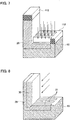
Fig. 5] Fig. 5 is a perspective diagram for explaining a method of manufacturing the semiconductor device according to the first embodiment of the present invention (part 1). - [
Fig. 6] Fig. 6 is a perspective diagram for explaining the method of manufacturing the semiconductor device according to the first embodiment of the present invention (part 2). - [
Fig. 7] Fig. 7 is a perspective diagram for explaining the method of manufacturing the semiconductor device according to the first embodiment of the present invention (part 3). - [
Fig. 8] Fig. 8 is a perspective diagram for explaining the method of manufacturing the semiconductor device according to the first embodiment of the present invention (part 4). - [
Fig. 9] Fig. 9 is a perspective diagram for explaining the method of manufacturing the semiconductor device according to the first embodiment of the present invention (part 5). - [
Fig. 10] Fig. 10 is a perspective diagram for explaining the method of manufacturing the semiconductor device according to the first embodiment of the present invention (part 6). - [
Fig. 11] Fig. 11 is a perspective diagram for explaining the method of manufacturing the semiconductor device according to the first embodiment of the present invention (part 7). - [
Fig. 12] Fig. 12 is a perspective diagram for explaining the method of manufacturing the semiconductor device according to the first embodiment of the present invention (part 8). - [
Fig. 13] Fig. 13 is a perspective diagram for explaining the method of manufacturing the semiconductor device according to the first embodiment of the present invention (part 9). - [
Fig. 14] Fig. 14 is a perspective diagram for explaining the method of manufacturing the semiconductor device according to the first embodiment of the present invention (part 10). - [
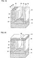
Fig. 15] Fig. 15 is a schematic perspective diagram illustrating the configuration of a semiconductor device according to a modification of the first embodiment of the present invention. - [
Fig. 16] Fig. 16 is a schematic perspective diagram illustrating the configuration of a semiconductor device according to a second embodiment of the present invention. - [
Fig. 17] Fig. 17 is a perspective diagram for explaining a method of manufacturing the semiconductor device according to the second embodiment of the present invention (part 1). - [
Fig. 18] Fig. 18 is a perspective diagram for explaining the method of manufacturing the semiconductor device according to the second embodiment of the present invention (part 2). - [
Fig. 19] Fig. 19 is a schematic perspective diagram illustrating the configuration of a semiconductor device according to a third embodiment of the present invention. - [
Fig. 20] Fig. 20 is a perspective diagram for explaining a method of manufacturing the semiconductor device according to the third embodiment of the present invention. - [
Fig. 21] Fig. 21 is a schematic perspective diagram illustrating the configuration of a semiconductor device according to a fourth embodiment of the present invention. - Hereinafter, embodiments will be described with reference to the drawings. The same portions in the illustration of the drawings are denoted by the same reference signs, and description thereof is omitted. Here, the drawings are schematically illustrated, and thus, the relationship between the thickness and the plane dimension, the ratio of the thicknesses of layers, and the like may be different from actual ones in the drawings. Also, there may be differences in the relationship or the ratio of dimensions between the drawings.
- A semiconductor device according to a first embodiment of the present invention includes, as illustrated in
Fig. 1 , asubstrate 10 having agroove 100 formed on its main surface, and adrift region 20,well region 30,first semiconductor region 40, andsecond semiconductor region 50 formed on thesubstrate 10. - The
drift region 20 is of a first conductivity type and has a portion disposed at a bottom part of thegroove 100. Note that in the embodiment illustrated inFig. 1 , thedrift region 20 is disposed to continue from one sidewall of the groove 100 (hereinafter referred to as the "first sidewall") to the bottom part of thegroove 100. - The
well region 30 which is of a second conductivity type is disposed in the first sidewall of thegroove 100 to be connected to thedrift region 20. Thewell region 30 illustrated inFig. 1 is disposed on the surface of thedrift region 20 in the first sidewall of thegroove 100, and the lower end of thewell region 30 is connected to thedrift region 20 at the bottom part of thegroove 100. - The
first semiconductor region 40 which is of the first conductivity type is disposed on the surface of thewell region 30 in the first sidewall of thegroove 100. Thefirst semiconductor region 40 is disposed on the surface of thewell region 30 not to extend over the outer edge of thewell region 30 so that thefirst semiconductor region 40 is isolated from thedrift region 20. Accordingly, as illustrated inFig. 1 , the lower end of thefirst semiconductor region 40 is positioned above the lower end of thewell region 30. - The
second semiconductor region 50 which is of the first conductivity type is disposed in thegroove 100 to be opposed to thewell region 30 via thedrift region 20. Thesecond semiconductor region 50 is connected to thedrift region 20 at a position away from thewell region 30. Thesecond semiconductor region 50 illustrated inFig. 2 is disposed at the bottom part of thegroove 100 to adjoin to thedrift region 20 to be close to the sidewall of thegroove 100 opposed to the first sidewall (hereinafter referred to as the "second sidewall"). - Note that the first conductivity type and the second conductivity type are conductivity types opposite to each other. Specifically, if the first conductivity type is n-type, then the second conductivity type is p-type. If the first conductivity type is p-type, then the second conductivity type is n-type. In the following, description is made as an example for the case where the first conductivity type is n-type and the second conductivity type is p-type.
- As described above, the semiconductor device illustrated in
Fig. 1 has, in the first sidewall of thegroove 100, thedrift region 20, thewell region 30, and thefirst semiconductor region 40, and those are layered along the direction of the normal line to the first sidewall (hereinafter referred to as the "lateral direction" of the groove 100). Then, openings are formed to extend over the upper surfaces of thedrift region 20, thewell region 30, and thefirst semiconductor region 40, and from the openings, multiple gate trenches are formed to extend in the depth direction of thegroove 100. The gate trenches have agate insulating film 65 disposed on their inner wall surfaces. The gate trenches are formed to reach thedrift region 20 disposed at the bottom part of thegroove 100. - As illustrated in
Fig. 1 , thegate insulating film 65 is formed continuously over thedrift region 20, thewell region 30, and thefirst semiconductor region 40 in the lateral direction. Inside the gate trench, agate electrode 60 is disposed to be opposed to thewell region 30 via thegate insulating film 65. - The semiconductor device illustrated in
Fig. 1 also includes a firstmain electrode 70 electrically connected to thefirst semiconductor region 40 and a secondmain electrode 80 electrically connected to thesecond semiconductor region 50. The firstmain electrode 70 is disposed on the surface of thefirst semiconductor region 40 in the first sidewall of thegroove 100. The secondmain electrode 80 is disposed in the second sidewall of thegroove 100 to be opposed to the firstmain electrode 70, and the lower end of the secondmain electrode 80 is in contact with thesecond semiconductor region 50 at the bottom part of thegroove 100. - The first
main electrode 70 is one end of the current route of the main electrical current that flows through the semiconductor device in the on state. The secondmain electrode 80 is the other end of the current route. The main electrical current of the semiconductor device flows between the firstmain electrode 70 and the secondmain electrode 80 via thefirst semiconductor region 40, thewell region 30, thedrift region 20, and thesecond semiconductor region 50. - As described later in detail, the semiconductor device illustrated in
Fig. 1 works as a transistor, and the main electrical current is controlled by applying a specified voltage to thegate electrodes 60 disposed in a middle of the current route. In the following, the semiconductor device is described based on the assumption that thefirst semiconductor region 40 is the source region, the firstmain electrode 70 is the source electrode, thesecond semiconductor region 50 is the drain region, and the secondmain electrode 80 is the drain electrode. - The
groove 100 is filled with anisolation insulating film 90. Specifically, theisolation insulating film 90 is disposed above thedrift region 20 disposed at the bottom part of thegroove 100 and between thesource electrode 70 and thedrain electrode 80. Thisisolation insulating film 90 insulates and isolates thedrift region 20 and thesource electrode 70 disposed above thedrift region 20 from each other.Fig. 1 illustrates the semiconductor device as if theisolation insulating film 90 were transparent to make it easy to understand the structure of the semiconductor device. In other words, only the outer edges are depicted for the isolation insulating film 90 (the same is true of other perspective diagrams). - Note that the regions outside the
groove 100, in other words, the regions outside the sidewall portion of thedrift region 20 and outside thedrain electrode 80, the illustration of which are omitted, are regions of thesubstrate 10 where thegroove 100 is not formed. - The portion of the
drift region 20 disposed at the bottom part of thegroove 100, illustrated inFig. 1 , has a structure in which an n-type drift region 21, which is a first conductivity type region, and a p-type drift region 22, which is a second conductivity type region, are disposed alternately in parallel with the main surface of thesubstrate 10 and along the direction in which thegroove 100 extends. In other words, the semiconductor device illustrated inFig. 1 has a super junction structure (SJ structure) in which multiple pn junctions are arranged at a constant cycle along the direction in which thegroove 100 extends (hereinafter referred to as the "longitudinal direction" of the groove 100). In semiconductor devices with the SJ structure, the main electrical current flows through the n-type drift regions 21 in which the concentration of n-type impurities is high in thedrift region 20, and this reduces the on-resistance. On the other hand, when a reverse bias is applied, the n-type drift regions 21 and the p-type drift regions 22 are depleted by depletion layers spreading from pn junctions, keeping high breakdown voltage. - In the semiconductor device illustrated in
Fig. 1 , channel regions are formed in the on state in thewell region 30 which is in contact with thegate insulating films 65. Hereinafter, the basic operation of the semiconductor device illustrated inFig. 1 will be described. - In the on operation, the semiconductor device functions as a transistor by the potential of the
gate electrodes 60 being controlled with respect to the potential of thesource electrode 70 in the state where a positive voltage is applied to thedrain electrode 80. Specifically, when the voltage between thegate electrodes 60 and thesource electrode 70 is a specified threshold voltage or higher, the inversion layers are formed in the channel regions in thewell region 30 on the side surfaces of thegate electrodes 60. This makes the semiconductor device in the on state, and the main electrical current flows between thedrain electrode 80 and thesource electrode 70. At this time, the main electrical current flows in thewell region 30 along the direction in parallel with the main surface of thesubstrate 10. InFig. 2 , the arrow I indicates the current route of the main electrical current of the semiconductor device in the on state. - For the off operation, the voltage between the
gate electrodes 60 and thesource electrode 70 is set to a specified threshold voltage or lower. This makes the inversion layers disappear, cutting off the main electrical current. - In the off state, depletion layers spread from the pn junction between the
well region 30 and thedrift region 20 toward thedrain region 50. At this time, as indicated by the arrows inFig. 3 , depletion layers 200 spread from the interfaces between the n-type drift regions 21 and the p-type drift regions 22. When the reverse voltage increases to a certain level, both the n-type drift regions 21 and the p-type drift regions 22 are completely depleted (which is called the pinch-off state). - When the n-
type drift regions 21 and the p-type drift regions 22 are in the pinch-off state, the electric field distribution of the n-type drift region 21 and the p-type drift region 22 becomes a uniform rectangle distribution, which greatly decreases the maximum electric field exerted on the semiconductor device. This improves the breakdown voltage of the semiconductor device. - In the semiconductor device illustrated in
Fig. 1 thesource region 40 and thesource electrode 70 are disposed above thedrift region 20 disposed at the bottom part of thegroove 100. Thus, unlike the structure having a source electrode and a drain electrode disposed on the respective sides of a gate electrode, the region immediately below thesource electrode 70 is an active region, which is not a region that does not contributes to the operation of the transistor. Hence, in the semiconductor device illustrated inFig. 1 , a region that does not contribute to the operation of the transistor is reduced, which makes it possible to reduce the chip area. - In addition, the
source region 40 and thewell region 30 are disposed in the first sidewall of thegroove 100, and the gate trenches are formed to extend in the depth direction of thegroove 100. Hence, in the on state, the end portion of the channel region extends in the depth direction along the first sidewall of thegroove 100. In other words, the channel region is formed to have a gate width of from the opening of thegroove 100 to the bottom part of thegroove 100. The wide channel region formed as described above reduces the on-resistance. - Further, the
source region 40 is formed in thegroove 100 along the first sidewall, and thesource region 40 extends in the depth direction of thegroove 100. This allows the contact portion between thesource region 40 and thesource electrode 70 formed along the first sidewall of thegroove 100 to extend in the depth direction of thegroove 100. This configuration makes it possible to increase the contact area without increasing the chip area, compared to the case of forming the contact portion between thesource region 40 and thesource electrode 70 to be in parallel with the main surface of thesubstrate 10. Thus, the contact resistance between thesource region 40 and thesource electrode 70 is reduced, which in turn reduces the on-resistance. - The semiconductor device illustrated in
Fig. 1 has a structure in which part of thedrift region 20 is disposed in the first sidewall of thegroove 100. Thus, when thewell region 30 opposed to thegate insulating films 65 induces channel charge, and the semiconductor device is turned to the on state, accumulated charge is generated at the boundary between thedrift region 20 and thegate insulating film 65 in the region surrounded by the dashed line A inFig. 4 . The current route caused by this accumulated charge is formed in parallel with the channel regions formed in thewell region 30, providing the effect of reducing resistance components in the channel regions of the semiconductor device. - Note that it is preferable that the
substrate 10 be an insulating substrate. Use of an insulating substrate simplifies the element separation process for the case where multiple semiconductor devices are integrated on onesubstrate 10. In the case where the semiconductor device is mounted on a cooling unit, an insulating substrate is not necessary between thesubstrate 10 and the cooling unit. Here, a substrate "having an insulating property" means that the resistivity of the substrate is several kΩcm or more. - For example, silicon carbide (SiC) having an insulating property is used for the
substrate 10. There are several polytypes (crystal polymorphs) of SiC, and a typical 4H-SiC substrate can be used for thesubstrate 10. - Use of a SiC substrate for the
substrate 10 provides a higher insulating property and a higher thermal conductivity of thesubstrate 10. This allows the semiconductor device to be cooled efficiently by attaching the back surface of thesubstrate 10 directly to a cooling mechanism. Since this structure provides a larger thermal conductivity in the SiC substrate, heat generation caused by the main electrical current when the semiconductor device is in the on state can be dissipated efficiency. SiC is a wide band gap semiconductor, in which the number of intrinsic carriers is small, and hence, it is easy to achieve a higher insulating property, and use of SiC makes it possible to achieve a semiconductor device with a high breakdown voltage. - Hereinafter, a method of manufacturing a semiconductor device according to the first embodiment of the present invention will be described with reference to the drawings. Note that the method of manufacturing a semiconductor device described below is an example, and thus, in addition to this method, various manufacturing methods including variations of this method are feasible.
- First, a
groove 100 is formed on the main surface of asubstrate 10 which is non-doped silicon carbide insulating semiconductor. The depth of thegroove 100 is, for example, approximately 10 to 20 µm, and the width in in the lateral direction is, for example, approximately 10 µm. - To form the
groove 100 by an etching method, amask material 111 is formed in a specified shape on the main surface of the substrate 10 (seeFig. 5 ). Themask material 111 may be, for example, a silicon oxide film, and the deposition method may be a thermal CVD method or a plasma CVD method. Then, a photoresist material on themask material 111 is patterned (not illustrated). For the patterning method, a general photolithography technique is used. The patterned photoresist material is used as a mask to etch themask material 111. For the etching method, a wet etching method using hydrofluoric acid or a dry etching method such as reactive ion etching is used. Next, the photoresist material is removed using oxygen plasma, sulfuric acid, or the like. Themask material 111 formed as described above is used as an etching mask to selectively etchsubstrate 10 by a dry etching method. Thus, thegroove 100 is formed as illustrated inFig. 5 . - After the
mask material 111 is removed, a portion of thedrift region 20 that is along thefirst sidewall 11 of the groove 100 (hereinafter referred to as a "sidewall portion" of the drift region 20) is formed by ion implantation or the like. For example, as the arrows indicate inFig. 6 , the sidewall portion of thedrift region 20 is formed by ion-implanting impurities of a first conductivity type obliquely from above the opening of thegroove 100 into the first sidewall. At this time, the impurities can be implanted only into the first sidewall of thegroove 100 by setting the angle at which the impurities are implanted into the first sidewall of thegroove 100, according to the aspect ratio determined from the depth and the width in in the lateral direction of thegroove 100. Through this process, the sidewall portion of thedrift region 20 is formed in the first sidewall of thegroove 100. Since the impurities are implanted from obliquely above, the lower end of the sidewall portion of thedrift region 20 reaches below the bottom part of thegroove 100. - Next, the n-
type drift regions 21 are formed in the portion of thedrift region 20 disposed at the bottom part of the groove 100 (hereinafter referred to as the "bottom portion" of the drift region 20). For example, as illustrated inFig. 7 , amask material 112 through which the regions of the bottom part of thegroove 100 to be the n-type drift regions 21 are exposed is formed by a photolithography technique. Then, the n-type drift regions 21 are formed selectively above thesubstrate 10 by ion-implanting impurities of the first conductivity type using themask material 112 as a mask. At this time, the impurities are implanted a little obliquely toward the first sidewall from the direction of the normal line to the main surface of thesubstrate 10, and thus, the impurities are implanted into portions below the sidewall portion of thedrift region 20. As a result, the sidewall portion and bottom portion of thedrift region 20 are connected to each other. After that, themask material 112 is removed. - Next a
well region 30 is formed in the first sidewall of thegroove 100 to be connected to thedrift region 20 by ion implantation or the like. For example, as arrows indicates inFig. 8 , thewell region 30 is formed to cover the sidewall portion of thedrift region 20 by ion-implanting impurities of a second conductivity type obliquely from above the opening of thegroove 100 into the first sidewall. At this time, the impurities can be implanted only into the first sidewall of thegroove 100 by setting the angle at which the impurities are implanted into the first sidewall of thegroove 100, according to the aspect ratio determined from the depth and the width in in the lateral direction of thegroove 100. Through this process, thewell region 30 is formed in the first sidewall of thegroove 100. - Since the impurities are implanted from obliquely above, the lower end of the
well region 30 reaches below the bottom part of thegroove 100. Note that the condition of the ion implantation is adjusted for thewell region 30 not to pass through thedrift region 20. The impurity concentration of thewell region 30 is, for example, approximately 1E15/cm3 to 1E19/cm3. - Next, the p-
type drift regions 22 are formed in the bottom portion of thedrift region 20. For example, as illustrated inFig. 9 , amask material 113 through which the regions of the bottom part of thegroove 100 to be the p-type drift regions 22 are exposed is formed, and then, the p-type drift regions 22 are formed selectively above thesubstrate 10 by ion-implanting impurities of the second conductivity type using themask material 113 used as a mask. Through this process, the bottom portion of thedrift region 20 is formed in which the n-type drift region and the p-type drift region are disposed alternately along the longitudinal direction of thegroove 100. After that, themask material 113 is removed. - For the ion implantation in the processes up to this point, for example, nitrogen (N) is used for the n-type impurities of the first conductivity type, and aluminum (Al) or boron (B) is used for the p-type impurities of the second conductivity type. Note that ion implantation is performed in the state where the
substrate 10 is heated to a temperature of approximately 600°C to prevent or reduce the occurrence of crystal defects in the ion-implanted regions. - Meanwhile, in order to completely deplete the SJ structure in the off state to achieve a high breakdown voltage, the ratio of the total amount of p-type impurities in the p-type drift region and the total amount of n-type impurities in the n-type drift region needs to be set to around 1. Hence, a high breakdown voltage can be achieved when Nd representing the concentration of n-type impurities in the n-
type drift region 21, Na representing the concentration of p-type impurities in the p-type drift region 22, Wn representing the width of the n-type drift region 21, and Wp representing the width of the p-type drift region 22 satisfy the following equation (1):
- Width Wn and width Wp are the widths in the direction in which the n-
type drift region 21 and the p-type drift region 22 are repeatedly arranged. The impurity concentrations of the n-type drift region 21 and the p-type drift region are set to satisfy equation (1). - For a semiconductor device of an SJ structure having the
drift region 20 that satisfies the above condition, the n-type drift regions 21 and the p-type drift regions 22 are depleted in the off state, which increases the breakdown voltage per unit area of thedrift region 20. Note that the impurity concentration of thedrift region 20 is, for example, approximately 1E15/cm3 to 1E19/cm3. - Next, a
source region 40 is formed on the surface of thewell region 30 in the first sidewall of thegroove 100. For example, as the arrows indicate inFig. 10 , thesource region 40 is formed in the region in which thewell region 30 has been formed by ion-implanting impurities of the first conductivity type obliquely from above the opening of thegroove 100 into the first sidewall. At this time, the impurities are implanted only into thewell region 30 of thegroove 100 by setting the angle at which the impurities are implanted into the first sidewall of thegroove 100, according to the aspect ratio determined from the depth and the width in in the lateral direction of thegroove 100. The impurity concentration of thesource region 40 is, for example, approximately 1E18/cm3 to 1E21/cm3. - Note that the
source region 40 is formed to be away from thedrift region 20. Accordingly, the impurity implantation angle of ion implantation to form thesource region 40 is set shallower than the impurity implantation angle of ion implantation to form thewell region 30. From this setting, the lower end of thesource region 40 is positioned above the lower end of thewell region 30, which prevents thesource region 40 from extending over to the outside of thewell region 30. - Next, a
drain region 50 is formed in thegroove 100 to be opposed to thewell region 30 via thedrift region 20. Thedrain region 50 is connected to thedrift region 20 at a position away from thewell region 30. For example, thedrain region 50 is formed selectively at the bottom part of thegroove 100 by ion-implanting impurities of the first conductivity type using, as a mask, amask material 114 formed such that a specified region is exposed through themask material 114 as illustrated inFig. 11 . The impurity concentration of thedrain region 50 is, for example, approximately 1E18/cm3 to 1E21/cm3. - After that, the ion-implanted impurities are activated by heat treatment. For example, heat treatment at around 1700°C is performed in argon atmosphere or nitrogen atmosphere.
- Next as illustrated in
Fig. 12 , openings are formed to extend over the upper surfaces of the sidewall portion of thedrift region 20, thewell region 30, and thesource region 40, andgate trenches 600 are formed to extend in the depth direction of thegroove 100. For example, a mask material formed on the upper surface of thesubstrate 10 is patterned by a photolithography technique, and then, thegate trenches 600 are formed by etching. Thegate trenches 600 are formed to have a width to reach the sidewall portion of thedrift region 20, thewell region 30, and thesource region 40 and a depth to reach thedrift region 20. - Next,
gate insulating films 65 are formed on the inner wall surfaces of thegate trenches 600. For example, the inner wall surfaces of thegate trenches 600 are oxidized to form thegate insulating films 65. The method of forming thegate insulating films 65 may be a thermal oxidization method or a deposition method. As an example, in the case of a thermal oxidization method, thesubstrate 10 is heated to a temperature at around 1100°C in oxygen atmosphere. After thegate insulating films 65 are formed, annealing at around 1000°C may be performed in the atmosphere of nitrogen, argon, N2O, or the like to decrease the interface state at the interface between thewell region 30 and thegate insulating films 65. Alternatively, thermal oxidation in NO or N2O atmosphere may be performed really. In that case, a temperature around 1100 to 1400°C is preferable. The thickness of thegate insulating film 65 is approximately several tens nm. - Next, as illustrated in
Fig. 13 , thegate electrodes 60 are formed inside thegate trenches 600. Thegate electrode 60 is opposed to thewell region 30 via thegate insulating film 65. Because a typical material of thegate electrode 60 is polysilicon films, here description is made of the case of using polysilicon films for thegate electrodes 60. - The deposition method of the polysilicon films may be a low-pressure CVD method or the like. For example, the thickness of a deposited polysilicon film is set to a value larger than half the width in the longitudinal direction of the opening of the
gate trench 600. Since a polysilicon film is formed from the inner wall surfaces of thegate trench 600, thegate trench 600 can be completely filled with a polysilicon film by setting the thickness of the polysilicon film as described above. For example, in the case where the width of thegate trench 600 is 2 µm, a polysilicon film is formed such that the film thickness is 1 µm or more. After the polysilicon film is deposited, an annealing treatment at 950°C is performed in phosphorus oxychloride POCl3 to form an n-type polysilicon film, which makes thegate electrode 60 conductive. - Next, the polysilicon film is planarized by etching. The etching method may be isotropic etching or anisotropic selective etching. The amount of etching is set such that the polysilicon film remains inside the
gate trench 600. For example, in the case where the width of thegate trench 600 is 2 µm, and a polysilicon film has been deposited to a thickness of 1.5 µm, the amount of etching for the polysilicon film should preferably be set to 1.5 µm. However, for the amount of etching of 1.5 µm, several percent over-etching in the control of etching will not cause any problem. - After that, as illustrated in
Fig. 14 , anisolation insulating film 90 is deposited on the upper surface of thesubstrate 10, and thegroove 100 is filled with theisolation insulating film 90. For theisolation insulating film 90, a silicon oxide film is typically preferable, and the deposition method may be a thermal CVD method or a plasma CVD method. - A resist film (not illustrated) formed on the upper surface of the
isolation insulating film 90 is patterned by a photolithography technique or the like, and this resist film is used as a mask to selectively remove parts of theisolation insulating film 90 in the regions where asource electrode 70 and adrain electrode 80 are to be formed. Through the process of selectively removing theisolation insulating film 90, contact holes in which the contact surface of thesource region 40 to be in contact with thesource electrode 70 and the contact surface of thedrain region 50 to be in contact with thedrain electrode 80 are exposed are formed in theisolation insulating film 90. The etching method for forming the contact holes may be a wet etching method using hydrofluoric acid or a dry etching method such as reactive ion etching. After that, the resist film is removed using oxygen plasma, sulfuric acid, or the like. - Then, the
source electrode 70 and thedrain electrode 80 are formed as illustrated inFig. 1 by filling the contact holes formed in theisolation insulating film 90. Thesource electrode 70 and thedrain electrode 80 are typically metal films. The materials of thesource electrode 70 and thedrain electrode 80 may be metal materials such as nickel (Ni) and molybdenum (Mo). Alternatively, laminated layer layers made of titanium (Ti), nickel (Ni), silver (Ag), or the like may be used for thesource electrode 70 and thedrain electrode 80. - The
source electrode 70 and thedrain electrode 80 may be formed by depositing a metal material on the entire surface by a sputtering method, an electron beam (EB) vapor deposition method, or the like and then etching the metal material by a dry etching method using a patterned resist film as a mask. Alternatively, thesource electrode 70 and thedrain electrode 80 may be formed by filling the contact holes formed in theisolation insulating film 90 with a metal material by a plating process. - Through the processes above, the semiconductor device illustrated in
Fig. 1 is completed. In the above, thedrift region 20 is formed by ion-implanting impurities into thesubstrate 10 having an insulating property. This eliminates the need for a process of epitaxial growth and reduces the manufacturing cost. - Similarly, since the
well region 30, thesource region 40, and thedrain region 50 are formed by ion-implantation impurities into thesubstrate 10, the manufacturing cost is lower than in the case of forming them by epitaxial growth. - In addition, the sidewall portion of the
drift region 20, thewell region 30 formed in the surface of this sidewall portion, and thesource region 40 formed in the surface of thewell region 30 are formed by ion-implanting impurities obliquely from the opening of thegroove 100 into the first sidewall. This process reduces the manufacturing cost and makes it possible to form these regions only in the first sidewall. - A semiconductor device according to a modification of the first embodiment, illustrated in
Fig. 15 has adrift region 20 disposed only at the bottom part of agroove 100. In other words, the semiconductor device according to the modification is different from the semiconductor device illustrated inFig. 1 in that thedrift region 20 is not disposed in the first sidewall of thegroove 100. - As illustrated in
Fig. 15 , the lower end of awell region 30 disposed in the first sidewall of thegroove 100 is connected to thedrift region 20 at the bottom part of thegroove 100. The openings of gate trenches are formed to extend over the upper surfaces of thewell region 30 and thefirst semiconductor region 40, andgate insulating films 65 andgate electrodes 60 are disposed inside the gate trenches. The gate trenches extend in the depth direction of thegroove 100 and pass through thewell region 30, and the lower ends of the gate trenches reach thedrift region 20. - Since the semiconductor device illustrated in
Fig. 15 does not have adrift region 20 in the first sidewall of thegroove 100, the manufacturing process is shorter, and the manufacturing cost is lower. - Also in the semiconductor device illustrated in
Fig. 15 , the region immediately below thesource electrode 70 is not a region that does not contribute to the operation of the transistor, which makes it possible to reduce the chip area. The channel regions are formed along the depth direction of thegroove 100 in the on state, which reduces the on-resistance. Further, thesource region 40 extends in the depth direction of thegroove 100, which reduces the contact resistance between thesource region 40 and thesource electrode 70. - Note that the semiconductor device according to the embodiment of the present invention does not need to have a
drift region 20 with a SJ structure, as illustrated inFig. 15 . In other words, the bottom portion of thedrift region 20 may be formed to be a single layer. - In a semiconductor device according to a second embodiment of the present invention, a
drift region 20 has, as illustrated inFig. 16 , a structure in which an n-type drift region 21 and a p-type drift region 22 are alternately layered along the depth direction of thegroove 100 at the bottom part of thegroove 100. Regarding the longitudinal direction of thegroove 100, each of the n-type drift region 21 and the p-type drift region is disposed to extend continuously over the entire surface, unlike the first embodiment having a structure in which an n-type drift region 21 and a p-type drift region are alternately disposed. Other configurations are the same as those of the first embodiment illustrated inFig. 1 . - The semiconductor device illustrated in
Fig. 16 operates in the same way as in the semiconductor device illustrated inFig. 1 . Specifically, when the voltage between thegate electrode 60 and thesource electrode 70 is a specified threshold voltage or higher, the inversion layers are formed in the channel regions in thewell region 30 at the side of thegate electrodes 60. This makes the semiconductor device in the on state. For the off operation, the voltage between thegate electrode 60 and thesource electrode 70 is set to a specified threshold voltage or lower. This makes the inversion layers disappear, cutting off the main electrical current. - In the off state, a depletion layer spreads from the interface between the n-
type drift region 21 and the p-type drift region 22 layered along the thickness direction of thegroove 100. When the n-type drift region 21 and the p-type drift region 22 are in the pinch-off state, the electric field distribution of the n-type drift region 21 and the p-type drift region 22 becomes a uniform rectangle distribution, greatly decreasing the maximum electric field exerted on the semiconductor device. This improves the breakdown voltage of the semiconductor device. - Hereinafter, an example of a method of manufacturing the semiconductor device according to the second embodiment will be described with reference to the drawings.
- In the same way as in the method described with reference to
Fig. 5 in the first embodiment, agroove 100 is formed on asubstrate 10. A substrate of a non-doped silicon carbide insulating semiconductor or the like is used for thesubstrate 10. - Then, the sidewall portion of a
drift region 20 and an n-type drift region 21 are formed as illustrated inFig. 17 by ion implantation using amask material 211, which has been patterned using a photolithography technique or the like, as a mask. Specifically, the sidewall portion of thedrift region 20 is formed in the first sidewall of thegroove 100 by ion-implanting impurities from obliquely above into the first sidewall of thegroove 100. Then, the n-type drift region 21 is formed at the bottom part of thegroove 100 by ion-implanting impurities into the main surface of thesubstrate 10. - After the
mask material 211 is removed, thewell region 30 and the p-type drift region 22 are formed by ion implantation using a newly formedmask material 212 as a mask as illustrated inFig. 18 . Specifically, thewell region 30 is formed in the first sidewall of thegroove 100 to be layered with the sidewall portion of thedrift region 20 by ion-implanting impurities from obliquely above into the first sidewall of thegroove 100. Then, a p-type drift region 22 is formed at the bottom part of thegroove 100 to be layered with the n-type drift region 21 by ion-implanting impurities into the main surface of thesubstrate 10. - After that, a
source region 40,drain region 50,gate insulating film 65,gate electrode 60,isolation insulating film 90,source electrode 70, and drainelectrode 80 are formed in the same way as in the method described with reference toFigs. 10 to 14 in the first embodiment. Through these processes, the semiconductor device illustrated inFig. 16 is completed. - The semiconductor device according to the second embodiment may require only one mask material to form the sidewall portion of the
drift region 20 and the n-type drift region 21 as described in the above manufacturing method. In addition, the semiconductor may require only one mask material to form thewell region 30 and the p-type drift region 22. Thus, it is possible to reduce the manufacturing cost. In addition, as in the first embodiment, the region immediately below thesource electrode 70 is not a region that does not contribute to the operation of the transistor, which makes it possible to reduce the chip area. The channel regions are formed along the depth direction of thegroove 100 in the on state, which reduces the on-resistance. Further, thesource region 40 extends in the depth direction of thegroove 100, which reduces the contact resistance between thesource region 40 and thesource electrode 70. - Note that the n-
type drift regions 21 and the p-type drift regions 22 may be alternately layered by repeating the process of forming the n-type drift region 21 and the process of forming the p-type drift region 22. These processes form a SJ structure having multiple pn junctions arranged at a constant cycle along the depth direction of thegroove 100. This configuration further improves the breakdown voltage of the semiconductor device. Other features are substantially the same as those of the first embodiment, and thus repetitive description thereof is omitted. - A semiconductor device according to a third embodiment of the present invention, as illustrated in
Fig. 19 , has a dividinggroove 900 that is formed in anisolation insulating film 90 disposed to fill the inside of thegroove 100 between thesource electrode 70 and thedrain electrode 80 and that extends in parallel with the first sidewall of thegroove 100. The dividinggroove 900 divides a portion of theisolation insulating film 90, sandwiched between thesource electrode 70 and thedrain electrode 80. Specifically, the semiconductor device illustrated inFig. 19 is different from the semiconductor device illustrated inFig. 1 in that the dividinggroove 900 divides theisolation insulating film 90 between thesource electrode 70 and thedrain electrode 80. Other configurations are the same as those of the first embodiment illustrated inFig. 1 . - For the semiconductor device illustrated in
Fig. 19 , the dividinggroove 900 formed in theisolation insulating film 90, which is a space provided between thesource electrode 70 and thedrain electrode 80, reduces the parasitic capacitance (Cds) between thesource electrode 70 and thedrain electrode 80. This in turn reduces the switching loss caused by charging and discharging with the output capacitance (Coss) in switching operation of the semiconductor device. - To reduce the parasitic capacitance (Cds), the depth of the dividing
groove 900 is set such that the dividinggroove 900 is formed at least in the region via which thesource electrode 70 and thedrain electrode 80 face each other. For example, the dividinggroove 900 is formed such that the bottom part of the dividinggroove 900 is positioned to be lower than the lower end of thesource electrode 70. - Note that even a small space formed in the
isolation insulating film 90 between thesource electrode 70 and thedrain electrode 80 can reduce the parasitic capacitance (Cds). For example, a dividinggroove 900 having a width of about several hundred nm to 1 µm is formed. - The
isolation insulating film 90 can be formed in the dividinggroove 900 by a dry etching method or the like. For example, as illustrated inFig. 20 , after theisolation insulating film 90 is formed, a resistfilm 311 is formed on the upper surface of theisolation insulating film 90 and patterned by a photolithography technique to remove part of the resistfilm 311 in the region where the dividinggroove 900 is to be formed. Then, theisolation insulating film 90 is selectively etched by a dry etching method using the resistfilm 311 as a mask to form the dividinggroove 900. Other features are substantially the same as those of the first embodiment, and thus repetitive description thereof is omitted. - A semiconductor device according to a fourth embodiment of the present invention, as illustrated in
Fig. 21 , has two semiconductor devices in onegroove 100 each having the same configuration as in the semiconductor device according to the first to the third embodiments. - Specifically, a
drain region 50 is disposed between a first sidewall and a second sidewall opposed to each other and at the bottom part in the center of thegroove 100, and adrain electrode 80 is disposed on the upper surface of thedrain region 50. Then, two semiconductor devices havingrespective source regions 40 disposed in the first sidewall and second sidewall of thegroove 100 are integrated. - The semiconductor devices illustrated in
Fig. 21 has aunit structure 1 including two semiconductor devices that share thedrain region 50 and thedrain electrode 80. Theunit structure 1, in which two semiconductor devices are disposed for onegroove 100 along the lateral direction of thegroove 100, improves the integration density. - Note that although
Fig. 21 illustrates only oneunit structure 1,multiple unit structures 1 may be connected along the lateral direction of thegroove 100, sharing thegate electrodes 60 of eachunit structure 1. Other features are substantially the same as those of the first to third embodiments, and thus repetitive description thereof is omitted. - Although the present invention has been described by showing embodiments as above, it should not be understood that the descriptions and drawings consisting part of this disclosure limit this invention. From this disclosure, various alternative embodiments, examples, and operational techniques will be apparent to those skilled in the art.
- For example, although an example in which a SiC substrate is used for the
substrate 10 has been described in the above, the material of thesubstrate 10 is not limited to a SiC substrate, but asubstrate 10 made of a semiconductor material having a wide band gap may be used. Examples of semiconductor materials having a wide band gap include GaN, diamond, ZnO, and AlGaN. - In addition, although an example in which an n-type polysilicon film is used for the
gate electrode 60 has been described, a p-type polysilicon film may be used for it. In addition, other semiconductor materials may be used for thegate electrode 60, or other conductive materials such as a metal material may be used. For example, poly-silicon carbide, SiGe, Al, or the like of the second conductivity type may be used for the material of thegate electrode 60. - Note that an example in which a silicon oxide film is used for the
gate insulating film 65 has been described, a silicon nitride film may be used for thegate insulating film 65. Alternatively, layered material of a silicon oxide film and a silicon nitride film may be used for thegate insulating film 65. Isotropic etching for the case where a silicon nitride film is used for thegate insulating film 65 can be performed by cleaning with hot phosphoric acid at 160°C. - In addition, although the above description is based on the assumption that the
first semiconductor region 40 is the source region and that thesecond semiconductor region 50 is the drain region, the semiconductor device may be configured such that thefirst semiconductor region 40 is the drain region and that thesecond semiconductor region 50 is the source region. - As above, it goes without saying that the present invention includes various embodiments and the like not described herein.
- The semiconductor device and method of manufacturing the same according to the present invention can be used in the electronics industry including a manufacturing industry that manufactures semiconductor devices in which the main electrical current flowing between two main electrodes is controlled.
-
- 10
- substrate
- 20
- drift region
- 21
- n-type drift region
- 22
- p-type drift region
- 30
- well region
- 40
- first semiconductor region
- 50
- second semiconductor region
- 60
- gate electrode
- 65
- gate insulating film
- 70
- first main electrode
- 80
- second main electrode
- 90
- isolation insulating film
Claims (10)
- A semiconductor device comprising:a substrate having a groove formed on a main surface of the substrate;a drift region of a first conductivity type, the drift region having a portion disposed at a bottom part of the groove;a well region of a second conductivity type, the well region being disposed in one sidewall of the groove to be connected to the drift region;a first semiconductor region of the first conductivity type, the first semiconductor region being disposed on a surface of the well region in the sidewall of the groove to be away from the drift region;a second semiconductor region of the first conductivity type, the second semiconductor region being disposed in the groove to be opposed to the well region via the drift region; anda gate electrode opposed to the well region, the gate electrode being disposed in a gate trench that has an opening extending over the upper surfaces of the well region and the first semiconductor region and extends in a depth direction of the groove.
- The semiconductor device according to claim 1, wherein the drift region is disposed to continue from the sidewall of the groove to the bottom part of the groove, and
the well region is disposed on a surface of the drift region in the sidewall of the groove. - The semiconductor device according to claim 1 or 2, wherein the substrate is an insulating substrate.
- The semiconductor device according to any one of claims 1 to 3, wherein
the portion of the drift region disposed at the bottom part of the groove has a structure in which a first conductivity type region and a second conductivity type region are disposed alternately along a longitudinal direction of the groove in which the sidewall extends. - The semiconductor device according to any one of claims 1 to 3, wherein
the portion of the drift region disposed at the bottom part of the groove has a structure in which a first conductivity type region and a second conductivity type region are layered along the depth direction of the groove. - The semiconductor device according to claim 4 or 5, wherein
impurity concentrations of the first conductivity type region and the second conductivity type region are set such that the first conductivity type region and the second conductivity type region are depleted by a depletion layer that spreads from a pn junction formed at the boundary between the first conductivity type region and the second conductivity type region, in an off state in which main electrical current flowing between the first semiconductor region and the second semiconductor region is cut off. - The semiconductor device according to any one of claims 1 to 6, further comprising:a first main electrode disposed on a surface of the first semiconductor region in the sidewall of the groove and electrically connected to the first semiconductor region;a second main electrode disposed in the groove to be opposed to the first main electrode and electrically connected to the second semiconductor region; andan isolation insulating film disposed between the first main electrode and the second main electrode and filling the inside of the groove, whereina portion of the isolation insulating film, the portion sandwiched between the first main electrode and the second main electrode, is divided by a dividing groove extending in parallel with the sidewall of the groove.
- A method of manufacturing a semiconductor device, comprising the steps of:forming a groove on a main surface of a substrate;forming a drift region of a first conductivity type, the drift region having a portion disposed at a bottom part of the groove;forming a well region of a second conductivity type in one sidewall of the groove such that the well region is connected to the drift region;forming a first semiconductor region of the first conductivity type on a surface of the well region in the sidewall of the groove such that the first semiconductor region is away from the drift region;forming a second semiconductor region of the first conductivity type in the groove such that the second semiconductor region is opposed to the well region via the drift region;forming a gate trench that has an opening extending over the upper surfaces of the well region and the first semiconductor region and extends in a depth direction of the groove; andforming a gate electrode opposed to the well region in the gate trench, whereinthe drift region is formed by ion-implanting impurities into the substrate.
- The method of manufacturing a semiconductor device according to claim 8, wherein
the well region, the first semiconductor region, and the second semiconductor region are formed by ion-implanting impurities into the substrate. - The method of manufacturing a semiconductor device according to claim 8 or 9, wherein
the drift region is formed to continue from the sidewall of the groove to the bottom part of the groove, and
a portion of the drift region, the portion formed in the sidewall of the groove; the well region formed on a surface of the drift region in the sidewall of the groove; and the first semiconductor region formed on the surface of the well region are formed by ion-implanting impurities obliquely from an opening of the groove into the sidewall of the groove.
Applications Claiming Priority (1)
| Application Number | Priority Date | Filing Date | Title |
|---|---|---|---|
| PCT/IB2018/000548 WO2019186224A1 (en) | 2018-03-26 | 2018-03-26 | Semiconductor device and method for manufacturing same |
Publications (3)
| Publication Number | Publication Date |
|---|---|
| EP3780071A1 true EP3780071A1 (en) | 2021-02-17 |
| EP3780071A4 EP3780071A4 (en) | 2021-03-10 |
| EP3780071B1 EP3780071B1 (en) | 2023-03-22 |
Family
ID=68060977
Family Applications (1)
| Application Number | Title | Priority Date | Filing Date |
|---|---|---|---|
| EP18912862.2A Active EP3780071B1 (en) | 2018-03-26 | 2018-03-26 | Semiconductor device and method for manufacturing same |
Country Status (5)
| Country | Link |
|---|---|
| US (1) | US12068411B2 (en) |
| EP (1) | EP3780071B1 (en) |
| JP (1) | JP6950816B2 (en) |
| CN (1) | CN111937123B (en) |
| WO (1) | WO2019186224A1 (en) |
Families Citing this family (3)
| Publication number | Priority date | Publication date | Assignee | Title |
|---|---|---|---|---|
| JP2023131941A (en) * | 2022-03-10 | 2023-09-22 | ソニーセミコンダクタソリューションズ株式会社 | semiconductor equipment |
| EP4325577B1 (en) * | 2022-04-14 | 2025-10-29 | Suzhou Loongspeed Semiconductor Technology Co., Ltd. | Transistor device and method for manufacturing same |
| JPWO2025022142A1 (en) * | 2023-07-24 | 2025-01-30 |
Family Cites Families (26)
| Publication number | Priority date | Publication date | Assignee | Title |
|---|---|---|---|---|
| JP3395473B2 (en) | 1994-10-25 | 2003-04-14 | 富士電機株式会社 | Horizontal trench MISFET and manufacturing method thereof |
| JP3395559B2 (en) * | 1997-01-28 | 2003-04-14 | 株式会社豊田中央研究所 | Semiconductor device |
| JP3641547B2 (en) * | 1998-03-25 | 2005-04-20 | 株式会社豊田中央研究所 | Semiconductor device including lateral MOS element |
| JP3943732B2 (en) * | 1998-10-27 | 2007-07-11 | 株式会社東芝 | High voltage semiconductor element |
| JP3356162B2 (en) * | 1999-10-19 | 2002-12-09 | 株式会社デンソー | Semiconductor device and manufacturing method thereof |
| JP3534084B2 (en) * | 2001-04-18 | 2004-06-07 | 株式会社デンソー | Semiconductor device and manufacturing method thereof |
| JP2003142684A (en) * | 2001-11-02 | 2003-05-16 | Toshiba Corp | Semiconductor element and semiconductor device |
| DE10309400B4 (en) * | 2003-03-04 | 2009-07-30 | Infineon Technologies Ag | Semiconductor device with increased dielectric strength and / or reduced on-resistance |
| US6960807B2 (en) * | 2003-11-25 | 2005-11-01 | Texas Instruments Incorporated | Drain extend MOS transistor with improved breakdown robustness |
| KR100790257B1 (en) * | 2006-12-27 | 2008-01-02 | 동부일렉트로닉스 주식회사 | Semiconductor device and manufacturing method |
| US7772668B2 (en) * | 2007-12-26 | 2010-08-10 | Fairchild Semiconductor Corporation | Shielded gate trench FET with multiple channels |
| JP2009302450A (en) * | 2008-06-17 | 2009-12-24 | Sharp Corp | Semiconductor device and its manufacturing method |
| JP5762689B2 (en) * | 2010-02-26 | 2015-08-12 | 株式会社東芝 | Semiconductor device |
| KR101396611B1 (en) * | 2010-04-28 | 2014-05-16 | 닛산 지도우샤 가부시키가이샤 | Semiconductor device |
| JP2012204563A (en) * | 2011-03-25 | 2012-10-22 | Toshiba Corp | Semiconductor element and semiconductor element manufacturing method |
| US9087894B2 (en) * | 2012-02-10 | 2015-07-21 | Panasonic Intellectual Property Management Co., Ltd. | Semiconductor device and method of manufacturing the device |
| JP2013201268A (en) * | 2012-03-23 | 2013-10-03 | Toshiba Corp | Semiconductor device |
| DE112013005062B4 (en) * | 2012-10-18 | 2020-10-01 | Mitsubishi Electric Corporation | Silicon carbide semiconductor device and manufacturing method of the same |
| JP6286823B2 (en) * | 2012-12-26 | 2018-03-07 | 日産自動車株式会社 | Manufacturing method of semiconductor device |
| KR101920717B1 (en) * | 2013-01-14 | 2018-11-21 | 삼성전자주식회사 | Semiconductor device including dual parallel channel structure and method of fabricating the same |
| CN105556647B (en) * | 2013-07-19 | 2017-06-13 | 日产自动车株式会社 | Semiconductor device and its manufacture method |
| CN104603949B (en) | 2014-01-27 | 2019-10-01 | 瑞萨电子株式会社 | Semiconductor devices |
| WO2015155828A1 (en) * | 2014-04-08 | 2015-10-15 | 日産自動車株式会社 | Semiconductor device and method for manufacturing same |
| US9178027B1 (en) * | 2014-08-12 | 2015-11-03 | Freescale Semiconductor, Inc. | Bidirectional trench FET with gate-based resurf |
| JP6477174B2 (en) * | 2015-04-02 | 2019-03-06 | 富士電機株式会社 | Semiconductor device and manufacturing method of semiconductor device |
| US10601413B2 (en) * | 2017-09-08 | 2020-03-24 | Cree, Inc. | Power switching devices with DV/DT capability and methods of making such devices |
-
2018
- 2018-03-26 CN CN201880091847.1A patent/CN111937123B/en active Active
- 2018-03-26 WO PCT/IB2018/000548 patent/WO2019186224A1/en not_active Ceased
- 2018-03-26 EP EP18912862.2A patent/EP3780071B1/en active Active
- 2018-03-26 US US17/040,631 patent/US12068411B2/en active Active
- 2018-03-26 JP JP2020510158A patent/JP6950816B2/en active Active
Also Published As
| Publication number | Publication date |
|---|---|
| CN111937123A (en) | 2020-11-13 |
| JPWO2019186224A1 (en) | 2021-04-08 |
| EP3780071B1 (en) | 2023-03-22 |
| US12068411B2 (en) | 2024-08-20 |
| JP6950816B2 (en) | 2021-10-13 |
| WO2019186224A1 (en) | 2019-10-03 |
| US20210367070A1 (en) | 2021-11-25 |
| CN111937123B (en) | 2025-04-11 |
| EP3780071A4 (en) | 2021-03-10 |
Similar Documents
| Publication | Publication Date | Title |
|---|---|---|
| JP7786512B2 (en) | Semiconductor Devices | |
| JP6569216B2 (en) | Insulated gate semiconductor device and manufacturing method thereof | |
| CN110291620B (en) | Semiconductor device and method of manufacturing the same | |
| JP2017092368A (en) | Semiconductor device and manufacturing method of semiconductor device | |
| EP3024018B1 (en) | Semiconductor device | |
| EP3780071B1 (en) | Semiconductor device and method for manufacturing same | |
| CN112005379B (en) | Semiconductor device and method for manufacturing the same | |
| JP6969684B2 (en) | Semiconductor devices and their manufacturing methods | |
| US11996442B2 (en) | Semiconductor device and method of manufacturing semiconductor device | |
| WO2025022142A1 (en) | Semiconductor device and manufacturing method for same | |
| JP2019096776A (en) | Semiconductor device and manufacturing method of the same | |
| EP4297100A1 (en) | Method for producing a semiconductor device and semiconductor device | |
| US11881526B2 (en) | Semiconductor device and method for manufacturing same | |
| EP1835543A1 (en) | Method for manufacturing semiconductor device | |
| JP2025047728A (en) | Semiconductor device and its manufacturing method | |
| JP2020205309A (en) | Semiconductor devices and their manufacturing methods |
Legal Events
| Date | Code | Title | Description |
|---|---|---|---|
| STAA | Information on the status of an ep patent application or granted ep patent |
Free format text: STATUS: THE INTERNATIONAL PUBLICATION HAS BEEN MADE |
|
| PUAI | Public reference made under article 153(3) epc to a published international application that has entered the european phase |
Free format text: ORIGINAL CODE: 0009012 |
|
| STAA | Information on the status of an ep patent application or granted ep patent |
Free format text: STATUS: REQUEST FOR EXAMINATION WAS MADE |
|
| 17P | Request for examination filed |
Effective date: 20200922 |
|
| AK | Designated contracting states |
Kind code of ref document: A1 Designated state(s): AL AT BE BG CH CY CZ DE DK EE ES FI FR GB GR HR HU IE IS IT LI LT LU LV MC MK MT NL NO PL PT RO RS SE SI SK SM TR |
|
| AX | Request for extension of the european patent |
Extension state: BA ME |
|
| A4 | Supplementary search report drawn up and despatched |
Effective date: 20210210 |
|
| RIC1 | Information provided on ipc code assigned before grant |
Ipc: H01L 21/336 20060101AFI20210204BHEP Ipc: H01L 29/78 20060101ALI20210204BHEP Ipc: H01L 29/08 20060101ALI20210204BHEP Ipc: H01L 21/28 20060101ALN20210204BHEP Ipc: H01L 29/06 20060101ALI20210204BHEP Ipc: H01L 29/417 20060101ALI20210204BHEP |
|
| DAV | Request for validation of the european patent (deleted) | ||
| DAX | Request for extension of the european patent (deleted) | ||
| RAP3 | Party data changed (applicant data changed or rights of an application transferred) |
Owner name: RENAULT S.A.S Owner name: NISSAN MOTOR CO., LTD. |
|
| RAP3 | Party data changed (applicant data changed or rights of an application transferred) |
Owner name: RENAULT S.A.S Owner name: NISSAN MOTOR CO., LTD. |
|
| GRAP | Despatch of communication of intention to grant a patent |
Free format text: ORIGINAL CODE: EPIDOSNIGR1 |
|
| STAA | Information on the status of an ep patent application or granted ep patent |
Free format text: STATUS: GRANT OF PATENT IS INTENDED |
|
| RIC1 | Information provided on ipc code assigned before grant |
Ipc: H01L 21/28 20060101ALN20221208BHEP Ipc: H01L 29/08 20060101ALI20221208BHEP Ipc: H01L 29/417 20060101ALI20221208BHEP Ipc: H01L 29/06 20060101ALI20221208BHEP Ipc: H01L 29/78 20060101ALI20221208BHEP Ipc: H01L 21/336 20060101AFI20221208BHEP |
|
| INTG | Intention to grant announced |
Effective date: 20221223 |
|
| RIC1 | Information provided on ipc code assigned before grant |
Ipc: H01L 21/28 20060101ALN20221212BHEP Ipc: H01L 29/08 20060101ALI20221212BHEP Ipc: H01L 29/417 20060101ALI20221212BHEP Ipc: H01L 29/06 20060101ALI20221212BHEP Ipc: H01L 29/78 20060101ALI20221212BHEP Ipc: H01L 21/336 20060101AFI20221212BHEP |
|
| GRAS | Grant fee paid |
Free format text: ORIGINAL CODE: EPIDOSNIGR3 |
|
| GRAA | (expected) grant |
Free format text: ORIGINAL CODE: 0009210 |
|
| STAA | Information on the status of an ep patent application or granted ep patent |
Free format text: STATUS: THE PATENT HAS BEEN GRANTED |
|
| AK | Designated contracting states |
Kind code of ref document: B1 Designated state(s): AL AT BE BG CH CY CZ DE DK EE ES FI FR GB GR HR HU IE IS IT LI LT LU LV MC MK MT NL NO PL PT RO RS SE SI SK SM TR |
|
| REG | Reference to a national code |
Ref country code: GB Ref legal event code: FG4D |
|
| REG | Reference to a national code |
Ref country code: CH Ref legal event code: EP |
|
| REG | Reference to a national code |
Ref country code: IE Ref legal event code: FG4D |
|
| REG | Reference to a national code |
Ref country code: AT Ref legal event code: REF Ref document number: 1555812 Country of ref document: AT Kind code of ref document: T Effective date: 20230415 |
|
| REG | Reference to a national code |
Ref country code: DE Ref legal event code: R096 Ref document number: 602018047636 Country of ref document: DE |
|
| REG | Reference to a national code |
Ref country code: LT Ref legal event code: MG9D |
|
| REG | Reference to a national code |
Ref country code: NL Ref legal event code: MP Effective date: 20230322 |
|
| PG25 | Lapsed in a contracting state [announced via postgrant information from national office to epo] |
Ref country code: RS Free format text: LAPSE BECAUSE OF FAILURE TO SUBMIT A TRANSLATION OF THE DESCRIPTION OR TO PAY THE FEE WITHIN THE PRESCRIBED TIME-LIMIT Effective date: 20230322 Ref country code: NO Free format text: LAPSE BECAUSE OF FAILURE TO SUBMIT A TRANSLATION OF THE DESCRIPTION OR TO PAY THE FEE WITHIN THE PRESCRIBED TIME-LIMIT Effective date: 20230622 Ref country code: LV Free format text: LAPSE BECAUSE OF FAILURE TO SUBMIT A TRANSLATION OF THE DESCRIPTION OR TO PAY THE FEE WITHIN THE PRESCRIBED TIME-LIMIT Effective date: 20230322 Ref country code: LT Free format text: LAPSE BECAUSE OF FAILURE TO SUBMIT A TRANSLATION OF THE DESCRIPTION OR TO PAY THE FEE WITHIN THE PRESCRIBED TIME-LIMIT Effective date: 20230322 Ref country code: HR Free format text: LAPSE BECAUSE OF FAILURE TO SUBMIT A TRANSLATION OF THE DESCRIPTION OR TO PAY THE FEE WITHIN THE PRESCRIBED TIME-LIMIT Effective date: 20230322 |
|
| REG | Reference to a national code |
Ref country code: AT Ref legal event code: MK05 Ref document number: 1555812 Country of ref document: AT Kind code of ref document: T Effective date: 20230322 |
|
| PG25 | Lapsed in a contracting state [announced via postgrant information from national office to epo] |
Ref country code: SE Free format text: LAPSE BECAUSE OF FAILURE TO SUBMIT A TRANSLATION OF THE DESCRIPTION OR TO PAY THE FEE WITHIN THE PRESCRIBED TIME-LIMIT Effective date: 20230322 Ref country code: NL Free format text: LAPSE BECAUSE OF FAILURE TO SUBMIT A TRANSLATION OF THE DESCRIPTION OR TO PAY THE FEE WITHIN THE PRESCRIBED TIME-LIMIT Effective date: 20230322 Ref country code: GR Free format text: LAPSE BECAUSE OF FAILURE TO SUBMIT A TRANSLATION OF THE DESCRIPTION OR TO PAY THE FEE WITHIN THE PRESCRIBED TIME-LIMIT Effective date: 20230623 Ref country code: FI Free format text: LAPSE BECAUSE OF FAILURE TO SUBMIT A TRANSLATION OF THE DESCRIPTION OR TO PAY THE FEE WITHIN THE PRESCRIBED TIME-LIMIT Effective date: 20230322 |
|
| PG25 | Lapsed in a contracting state [announced via postgrant information from national office to epo] |
Ref country code: SM Free format text: LAPSE BECAUSE OF FAILURE TO SUBMIT A TRANSLATION OF THE DESCRIPTION OR TO PAY THE FEE WITHIN THE PRESCRIBED TIME-LIMIT Effective date: 20230322 Ref country code: RO Free format text: LAPSE BECAUSE OF FAILURE TO SUBMIT A TRANSLATION OF THE DESCRIPTION OR TO PAY THE FEE WITHIN THE PRESCRIBED TIME-LIMIT Effective date: 20230322 Ref country code: PT Free format text: LAPSE BECAUSE OF FAILURE TO SUBMIT A TRANSLATION OF THE DESCRIPTION OR TO PAY THE FEE WITHIN THE PRESCRIBED TIME-LIMIT Effective date: 20230724 Ref country code: ES Free format text: LAPSE BECAUSE OF FAILURE TO SUBMIT A TRANSLATION OF THE DESCRIPTION OR TO PAY THE FEE WITHIN THE PRESCRIBED TIME-LIMIT Effective date: 20230322 Ref country code: EE Free format text: LAPSE BECAUSE OF FAILURE TO SUBMIT A TRANSLATION OF THE DESCRIPTION OR TO PAY THE FEE WITHIN THE PRESCRIBED TIME-LIMIT Effective date: 20230322 Ref country code: AT Free format text: LAPSE BECAUSE OF FAILURE TO SUBMIT A TRANSLATION OF THE DESCRIPTION OR TO PAY THE FEE WITHIN THE PRESCRIBED TIME-LIMIT Effective date: 20230322 |
|
| REG | Reference to a national code |
Ref country code: CH Ref legal event code: PL |
|
| PG25 | Lapsed in a contracting state [announced via postgrant information from national office to epo] |
Ref country code: SK Free format text: LAPSE BECAUSE OF FAILURE TO SUBMIT A TRANSLATION OF THE DESCRIPTION OR TO PAY THE FEE WITHIN THE PRESCRIBED TIME-LIMIT Effective date: 20230322 Ref country code: PL Free format text: LAPSE BECAUSE OF FAILURE TO SUBMIT A TRANSLATION OF THE DESCRIPTION OR TO PAY THE FEE WITHIN THE PRESCRIBED TIME-LIMIT Effective date: 20230322 Ref country code: IS Free format text: LAPSE BECAUSE OF FAILURE TO SUBMIT A TRANSLATION OF THE DESCRIPTION OR TO PAY THE FEE WITHIN THE PRESCRIBED TIME-LIMIT Effective date: 20230722 |
|
| REG | Reference to a national code |
Ref country code: BE Ref legal event code: MM Effective date: 20230331 |
|
| PG25 | Lapsed in a contracting state [announced via postgrant information from national office to epo] |
Ref country code: LU Free format text: LAPSE BECAUSE OF NON-PAYMENT OF DUE FEES Effective date: 20230326 |
|
| REG | Reference to a national code |
Ref country code: DE Ref legal event code: R097 Ref document number: 602018047636 Country of ref document: DE |
|
| PG25 | Lapsed in a contracting state [announced via postgrant information from national office to epo] |
Ref country code: MC Free format text: LAPSE BECAUSE OF FAILURE TO SUBMIT A TRANSLATION OF THE DESCRIPTION OR TO PAY THE FEE WITHIN THE PRESCRIBED TIME-LIMIT Effective date: 20230322 |
|
| REG | Reference to a national code |
Ref country code: IE Ref legal event code: MM4A |
|
| PLBE | No opposition filed within time limit |
Free format text: ORIGINAL CODE: 0009261 |
|
| STAA | Information on the status of an ep patent application or granted ep patent |
Free format text: STATUS: NO OPPOSITION FILED WITHIN TIME LIMIT |
|
| PG25 | Lapsed in a contracting state [announced via postgrant information from national office to epo] |
Ref country code: SI Free format text: LAPSE BECAUSE OF FAILURE TO SUBMIT A TRANSLATION OF THE DESCRIPTION OR TO PAY THE FEE WITHIN THE PRESCRIBED TIME-LIMIT Effective date: 20230322 Ref country code: MC Free format text: LAPSE BECAUSE OF FAILURE TO SUBMIT A TRANSLATION OF THE DESCRIPTION OR TO PAY THE FEE WITHIN THE PRESCRIBED TIME-LIMIT Effective date: 20230322 Ref country code: IE Free format text: LAPSE BECAUSE OF NON-PAYMENT OF DUE FEES Effective date: 20230326 Ref country code: DK Free format text: LAPSE BECAUSE OF FAILURE TO SUBMIT A TRANSLATION OF THE DESCRIPTION OR TO PAY THE FEE WITHIN THE PRESCRIBED TIME-LIMIT Effective date: 20230322 Ref country code: CZ Free format text: LAPSE BECAUSE OF FAILURE TO SUBMIT A TRANSLATION OF THE DESCRIPTION OR TO PAY THE FEE WITHIN THE PRESCRIBED TIME-LIMIT Effective date: 20230322 Ref country code: CH Free format text: LAPSE BECAUSE OF NON-PAYMENT OF DUE FEES Effective date: 20230331 Ref country code: LI Free format text: LAPSE BECAUSE OF NON-PAYMENT OF DUE FEES Effective date: 20230331 |
|
| 26N | No opposition filed |
Effective date: 20240102 |
|
| PG25 | Lapsed in a contracting state [announced via postgrant information from national office to epo] |
Ref country code: BE Free format text: LAPSE BECAUSE OF NON-PAYMENT OF DUE FEES Effective date: 20230331 |
|
| PG25 | Lapsed in a contracting state [announced via postgrant information from national office to epo] |
Ref country code: IT Free format text: LAPSE BECAUSE OF FAILURE TO SUBMIT A TRANSLATION OF THE DESCRIPTION OR TO PAY THE FEE WITHIN THE PRESCRIBED TIME-LIMIT Effective date: 20230322 |
|
| PG25 | Lapsed in a contracting state [announced via postgrant information from national office to epo] |
Ref country code: BG Free format text: LAPSE BECAUSE OF FAILURE TO SUBMIT A TRANSLATION OF THE DESCRIPTION OR TO PAY THE FEE WITHIN THE PRESCRIBED TIME-LIMIT Effective date: 20230322 |
|
| REG | Reference to a national code |
Ref country code: DE Ref legal event code: R079 Ref document number: 602018047636 Country of ref document: DE Free format text: PREVIOUS MAIN CLASS: H01L0021336000 Ipc: H10D0030010000 |
|
| PG25 | Lapsed in a contracting state [announced via postgrant information from national office to epo] |
Ref country code: BG Free format text: LAPSE BECAUSE OF FAILURE TO SUBMIT A TRANSLATION OF THE DESCRIPTION OR TO PAY THE FEE WITHIN THE PRESCRIBED TIME-LIMIT Effective date: 20230322 |
|
| PG25 | Lapsed in a contracting state [announced via postgrant information from national office to epo] |
Ref country code: CY Free format text: LAPSE BECAUSE OF FAILURE TO SUBMIT A TRANSLATION OF THE DESCRIPTION OR TO PAY THE FEE WITHIN THE PRESCRIBED TIME-LIMIT; INVALID AB INITIO Effective date: 20180326 |
|
| PG25 | Lapsed in a contracting state [announced via postgrant information from national office to epo] |
Ref country code: HU Free format text: LAPSE BECAUSE OF FAILURE TO SUBMIT A TRANSLATION OF THE DESCRIPTION OR TO PAY THE FEE WITHIN THE PRESCRIBED TIME-LIMIT; INVALID AB INITIO Effective date: 20180326 |
|
| PG25 | Lapsed in a contracting state [announced via postgrant information from national office to epo] |
Ref country code: TR Free format text: LAPSE BECAUSE OF FAILURE TO SUBMIT A TRANSLATION OF THE DESCRIPTION OR TO PAY THE FEE WITHIN THE PRESCRIBED TIME-LIMIT Effective date: 20230322 |
|
| PGFP | Annual fee paid to national office [announced via postgrant information from national office to epo] |
Ref country code: GB Payment date: 20260219 Year of fee payment: 9 |
|
| PGFP | Annual fee paid to national office [announced via postgrant information from national office to epo] |
Ref country code: DE Payment date: 20260219 Year of fee payment: 9 |
|
| PGFP | Annual fee paid to national office [announced via postgrant information from national office to epo] |
Ref country code: FR Payment date: 20260219 Year of fee payment: 9 |