EP3779597A1 - Black barrier wall pattern film and method for manufacturing same - Google Patents
Black barrier wall pattern film and method for manufacturing same Download PDFInfo
- Publication number
- EP3779597A1 EP3779597A1 EP19777058.9A EP19777058A EP3779597A1 EP 3779597 A1 EP3779597 A1 EP 3779597A1 EP 19777058 A EP19777058 A EP 19777058A EP 3779597 A1 EP3779597 A1 EP 3779597A1
- Authority
- EP
- European Patent Office
- Prior art keywords
- black
- partition wall
- wall pattern
- film
- curable resin
- Prior art date
- Legal status (The legal status is an assumption and is not a legal conclusion. Google has not performed a legal analysis and makes no representation as to the accuracy of the status listed.)
- Granted
Links
Images


Classifications
-
- G—PHYSICS
- G03—PHOTOGRAPHY; CINEMATOGRAPHY; ANALOGOUS TECHNIQUES USING WAVES OTHER THAN OPTICAL WAVES; ELECTROGRAPHY; HOLOGRAPHY
- G03F—PHOTOMECHANICAL PRODUCTION OF TEXTURED OR PATTERNED SURFACES, e.g. FOR PRINTING, FOR PROCESSING OF SEMICONDUCTOR DEVICES; MATERIALS THEREFOR; ORIGINALS THEREFOR; APPARATUS SPECIALLY ADAPTED THEREFOR
- G03F7/00—Photomechanical, e.g. photolithographic, production of textured or patterned surfaces, e.g. printing surfaces; Materials therefor, e.g. comprising photoresists; Apparatus specially adapted therefor
- G03F7/0002—Lithographic processes using patterning methods other than those involving the exposure to radiation, e.g. by stamping
-
- E—FIXED CONSTRUCTIONS
- E06—DOORS, WINDOWS, SHUTTERS, OR ROLLER BLINDS IN GENERAL; LADDERS
- E06B—FIXED OR MOVABLE CLOSURES FOR OPENINGS IN BUILDINGS, VEHICLES, FENCES OR LIKE ENCLOSURES IN GENERAL, e.g. DOORS, WINDOWS, BLINDS, GATES
- E06B9/00—Screening or protective devices for wall or similar openings, with or without operating or securing mechanisms; Closures of similar construction
- E06B9/24—Screens or other constructions affording protection against light, especially against sunshine; Similar screens for privacy or appearance; Slat blinds
-
- G—PHYSICS
- G02—OPTICS
- G02F—OPTICAL DEVICES OR ARRANGEMENTS FOR THE CONTROL OF LIGHT BY MODIFICATION OF THE OPTICAL PROPERTIES OF THE MEDIA OF THE ELEMENTS INVOLVED THEREIN; NON-LINEAR OPTICS; FREQUENCY-CHANGING OF LIGHT; OPTICAL LOGIC ELEMENTS; OPTICAL ANALOGUE/DIGITAL CONVERTERS
- G02F1/00—Devices or arrangements for the control of the intensity, colour, phase, polarisation or direction of light arriving from an independent light source, e.g. switching, gating or modulating; Non-linear optics
- G02F1/01—Devices or arrangements for the control of the intensity, colour, phase, polarisation or direction of light arriving from an independent light source, e.g. switching, gating or modulating; Non-linear optics for the control of the intensity, phase, polarisation or colour
- G02F1/165—Devices or arrangements for the control of the intensity, colour, phase, polarisation or direction of light arriving from an independent light source, e.g. switching, gating or modulating; Non-linear optics for the control of the intensity, phase, polarisation or colour based on translational movement of particles in a fluid under the influence of an applied field
- G02F1/166—Devices or arrangements for the control of the intensity, colour, phase, polarisation or direction of light arriving from an independent light source, e.g. switching, gating or modulating; Non-linear optics for the control of the intensity, phase, polarisation or colour based on translational movement of particles in a fluid under the influence of an applied field characterised by the electro-optical or magneto-optical effect
- G02F1/167—Devices or arrangements for the control of the intensity, colour, phase, polarisation or direction of light arriving from an independent light source, e.g. switching, gating or modulating; Non-linear optics for the control of the intensity, phase, polarisation or colour based on translational movement of particles in a fluid under the influence of an applied field characterised by the electro-optical or magneto-optical effect by electrophoresis
-
- G—PHYSICS
- G02—OPTICS
- G02F—OPTICAL DEVICES OR ARRANGEMENTS FOR THE CONTROL OF LIGHT BY MODIFICATION OF THE OPTICAL PROPERTIES OF THE MEDIA OF THE ELEMENTS INVOLVED THEREIN; NON-LINEAR OPTICS; FREQUENCY-CHANGING OF LIGHT; OPTICAL LOGIC ELEMENTS; OPTICAL ANALOGUE/DIGITAL CONVERTERS
- G02F1/00—Devices or arrangements for the control of the intensity, colour, phase, polarisation or direction of light arriving from an independent light source, e.g. switching, gating or modulating; Non-linear optics
- G02F1/01—Devices or arrangements for the control of the intensity, colour, phase, polarisation or direction of light arriving from an independent light source, e.g. switching, gating or modulating; Non-linear optics for the control of the intensity, phase, polarisation or colour
- G02F1/165—Devices or arrangements for the control of the intensity, colour, phase, polarisation or direction of light arriving from an independent light source, e.g. switching, gating or modulating; Non-linear optics for the control of the intensity, phase, polarisation or colour based on translational movement of particles in a fluid under the influence of an applied field
- G02F1/1675—Constructional details
- G02F1/1679—Gaskets; Spacers; Sealing of cells; Filling or closing of cells
- G02F1/1681—Gaskets; Spacers; Sealing of cells; Filling or closing of cells having two or more microcells partitioned by walls, e.g. of microcup type
-
- G—PHYSICS
- G03—PHOTOGRAPHY; CINEMATOGRAPHY; ANALOGOUS TECHNIQUES USING WAVES OTHER THAN OPTICAL WAVES; ELECTROGRAPHY; HOLOGRAPHY
- G03F—PHOTOMECHANICAL PRODUCTION OF TEXTURED OR PATTERNED SURFACES, e.g. FOR PRINTING, FOR PROCESSING OF SEMICONDUCTOR DEVICES; MATERIALS THEREFOR; ORIGINALS THEREFOR; APPARATUS SPECIALLY ADAPTED THEREFOR
- G03F7/00—Photomechanical, e.g. photolithographic, production of textured or patterned surfaces, e.g. printing surfaces; Materials therefor, e.g. comprising photoresists; Apparatus specially adapted therefor
- G03F7/0005—Production of optical devices or components in so far as characterised by the lithographic processes or materials used therefor
- G03F7/0007—Filters, e.g. additive colour filters; Components for display devices
-
- G—PHYSICS
- G03—PHOTOGRAPHY; CINEMATOGRAPHY; ANALOGOUS TECHNIQUES USING WAVES OTHER THAN OPTICAL WAVES; ELECTROGRAPHY; HOLOGRAPHY
- G03F—PHOTOMECHANICAL PRODUCTION OF TEXTURED OR PATTERNED SURFACES, e.g. FOR PRINTING, FOR PROCESSING OF SEMICONDUCTOR DEVICES; MATERIALS THEREFOR; ORIGINALS THEREFOR; APPARATUS SPECIALLY ADAPTED THEREFOR
- G03F7/00—Photomechanical, e.g. photolithographic, production of textured or patterned surfaces, e.g. printing surfaces; Materials therefor, e.g. comprising photoresists; Apparatus specially adapted therefor
- G03F7/004—Photosensitive materials
- G03F7/027—Non-macromolecular photopolymerisable compounds having carbon-to-carbon double bonds, e.g. ethylenic compounds
-
- G—PHYSICS
- G03—PHOTOGRAPHY; CINEMATOGRAPHY; ANALOGOUS TECHNIQUES USING WAVES OTHER THAN OPTICAL WAVES; ELECTROGRAPHY; HOLOGRAPHY
- G03F—PHOTOMECHANICAL PRODUCTION OF TEXTURED OR PATTERNED SURFACES, e.g. FOR PRINTING, FOR PROCESSING OF SEMICONDUCTOR DEVICES; MATERIALS THEREFOR; ORIGINALS THEREFOR; APPARATUS SPECIALLY ADAPTED THEREFOR
- G03F7/00—Photomechanical, e.g. photolithographic, production of textured or patterned surfaces, e.g. printing surfaces; Materials therefor, e.g. comprising photoresists; Apparatus specially adapted therefor
- G03F7/004—Photosensitive materials
- G03F7/027—Non-macromolecular photopolymerisable compounds having carbon-to-carbon double bonds, e.g. ethylenic compounds
- G03F7/028—Non-macromolecular photopolymerisable compounds having carbon-to-carbon double bonds, e.g. ethylenic compounds with photosensitivity-increasing substances, e.g. photoinitiators
-
- G—PHYSICS
- G03—PHOTOGRAPHY; CINEMATOGRAPHY; ANALOGOUS TECHNIQUES USING WAVES OTHER THAN OPTICAL WAVES; ELECTROGRAPHY; HOLOGRAPHY
- G03F—PHOTOMECHANICAL PRODUCTION OF TEXTURED OR PATTERNED SURFACES, e.g. FOR PRINTING, FOR PROCESSING OF SEMICONDUCTOR DEVICES; MATERIALS THEREFOR; ORIGINALS THEREFOR; APPARATUS SPECIALLY ADAPTED THEREFOR
- G03F7/00—Photomechanical, e.g. photolithographic, production of textured or patterned surfaces, e.g. printing surfaces; Materials therefor, e.g. comprising photoresists; Apparatus specially adapted therefor
- G03F7/004—Photosensitive materials
- G03F7/09—Photosensitive materials characterised by structural details, e.g. supports, auxiliary layers
- G03F7/105—Photosensitive materials characterised by structural details, e.g. supports, auxiliary layers having substances, e.g. indicators, for forming visible images
-
- G—PHYSICS
- G03—PHOTOGRAPHY; CINEMATOGRAPHY; ANALOGOUS TECHNIQUES USING WAVES OTHER THAN OPTICAL WAVES; ELECTROGRAPHY; HOLOGRAPHY
- G03F—PHOTOMECHANICAL PRODUCTION OF TEXTURED OR PATTERNED SURFACES, e.g. FOR PRINTING, FOR PROCESSING OF SEMICONDUCTOR DEVICES; MATERIALS THEREFOR; ORIGINALS THEREFOR; APPARATUS SPECIALLY ADAPTED THEREFOR
- G03F7/00—Photomechanical, e.g. photolithographic, production of textured or patterned surfaces, e.g. printing surfaces; Materials therefor, e.g. comprising photoresists; Apparatus specially adapted therefor
- G03F7/16—Coating processes; Apparatus therefor
- G03F7/168—Finishing the coated layer, e.g. drying, baking, soaking
-
- G—PHYSICS
- G03—PHOTOGRAPHY; CINEMATOGRAPHY; ANALOGOUS TECHNIQUES USING WAVES OTHER THAN OPTICAL WAVES; ELECTROGRAPHY; HOLOGRAPHY
- G03F—PHOTOMECHANICAL PRODUCTION OF TEXTURED OR PATTERNED SURFACES, e.g. FOR PRINTING, FOR PROCESSING OF SEMICONDUCTOR DEVICES; MATERIALS THEREFOR; ORIGINALS THEREFOR; APPARATUS SPECIALLY ADAPTED THEREFOR
- G03F7/00—Photomechanical, e.g. photolithographic, production of textured or patterned surfaces, e.g. printing surfaces; Materials therefor, e.g. comprising photoresists; Apparatus specially adapted therefor
- G03F7/20—Exposure; Apparatus therefor
- G03F7/2002—Exposure; Apparatus therefor with visible light or UV light, through an original having an opaque pattern on a transparent support, e.g. film printing, projection printing; by reflection of visible or UV light from an original such as a printed image
- G03F7/2004—Exposure; Apparatus therefor with visible light or UV light, through an original having an opaque pattern on a transparent support, e.g. film printing, projection printing; by reflection of visible or UV light from an original such as a printed image characterised by the use of a particular light source, e.g. fluorescent lamps or deep UV light
-
- E—FIXED CONSTRUCTIONS
- E06—DOORS, WINDOWS, SHUTTERS, OR ROLLER BLINDS IN GENERAL; LADDERS
- E06B—FIXED OR MOVABLE CLOSURES FOR OPENINGS IN BUILDINGS, VEHICLES, FENCES OR LIKE ENCLOSURES IN GENERAL, e.g. DOORS, WINDOWS, BLINDS, GATES
- E06B9/00—Screening or protective devices for wall or similar openings, with or without operating or securing mechanisms; Closures of similar construction
- E06B9/24—Screens or other constructions affording protection against light, especially against sunshine; Similar screens for privacy or appearance; Slat blinds
- E06B2009/2464—Screens or other constructions affording protection against light, especially against sunshine; Similar screens for privacy or appearance; Slat blinds featuring transparency control by applying voltage, e.g. LCD, electrochromic panels
Definitions
- the present application relates to a black partition wall pattern film and a method of manufacturing the same.
- An electrophoretic variable transmittance film is easy to transmit and block light entering from outside and thus may be used as a smart window for building, a sunroof for a vehicle, and a light blocking film for a transparent display.
- FIG. 1 is a view illustrating an operating principle of an electrophoretic variable transmittance film in the related art which operates in a light blocking mode or a light transmitting mode.
- a positive voltage is applied to a metal electrode pattern, and negatively charged nanoparticles are concentrated on the metal electrode pattern having a relatively small electrode width, such that the light blocking mode may be converted into the light transmitting mode.
- the present application has been made in an effort to provide a black partition wall pattern film and a method of manufacturing the same.
- An exemplary embodiment of the present application provides a black partition wall pattern film comprising: a transparent substrate; an electrode layer provided on the transparent substrate; a black partition wall pattern provided on the electrode layer; and a black UV-curable resin layer provided in a region on the electrode layer where no black partition wall pattern is provided.
- another exemplary embodiment of the present application provides a method of manufacturing the black partition wall pattern film, the method comprising: forming an electrode layer on a transparent substrate; applying a black UV-curable resin composition onto the electrode layer; pressing the applied black UV-curable resin composition with an imprinting mold and then curing the black UV-curable resin composition; and removing the imprinting mold.
- variable transmittance film comprising the black partition wall pattern film.
- the black partition wall pattern is comprised, it is possible to prevent the transmittance from increasing in the light blocking mode when the exemplary embodiment is applied to an electrophoretic smart window.
- the black partition wall pattern film may be manufactured by using the imprinting process, it is possible to simplify the process of manufacturing the black partition wall pattern film and to form the black partition wall pattern having a desired line width.
- the term "transparent” means that transmittance is about 80% or higher in a visible ray region (400 nm to 700 nm).
- a variable transmittance film in the related art is schematically illustrated in FIG. 1 .
- the present application provides a black partition wall pattern film and a method of manufacturing the same which are capable of solving the above-mentioned problems.
- a black partition wall pattern film comprises: a transparent substrate; an electrode layer provided on the transparent substrate; a black partition wall pattern provided on the electrode layer; and a black UV-curable resin layer provided in a region on the electrode layer where no black partition wall pattern is provided.
- the transparent substrate may be, but not limited to, a glass base or a transparent plastic base which is excellent in transparency, surface smoothness, tractability, and waterproofness, and the transparent base is not limited as long as the transparent base is typically used for electronic elements.
- the transparent base may be made of glass; urethane resin; polyimide resin; polyester resin; (meth)acrylate-based polymeric resin; or polyolefin-based resin such as polyethylene or polypropylene.
- the electrode layer may comprise a transparent conductive oxide. More specifically, the electrode layer may comprise, but not limited only to, one or more of an indium oxide, a zinc oxide, an indium tin oxide, an indium zinc oxide, and an indium zinc tin oxide.
- surface resistance of the electrode layer may be 200 ⁇ /sq. or less.
- a line height of the black partition wall pattern may be 5 ⁇ m or more, and a line width of the black partition wall pattern may be 30 ⁇ m or less.
- a line height of the black partition wall pattern may be 5 ⁇ m to 50 ⁇ m, and a line width of the black partition wall pattern may be 5 ⁇ m to 30 ⁇ m.
- the line height of the black partition wall pattern is less than 5 ⁇ m, a distance between a transparent electrode and a metal electrode pattern substrate is decreased, such that the content of negatively (-) charged nanoparticles in a dispersion liquid is excessively increased in order to ensure the transmittance of 1% or less in the light blocking mode, and as a result, there may be a problem in that a dispersion property of the negatively (-) charged nanoparticles deteriorates when a variable transmittance element operates.
- the line height of the black partition wall pattern is more than 50 ⁇ m, the distance between the transparent electrode and the metal electrode pattern substrate is increased, and as a result, an operating speed may be decreased.
- a cell gap between the electrodes may be determined based on the line height of the black partition wall pattern. More specifically, if the cell gap is small, concentration of a light blocking dispersion liquid may be increased in order to ensure a light blocking property, and an excessive increase in concentration of charged particles may degrade dispersion stability. In addition, if the cell gap is large, intensity of an electric field formed between the transparent electrode and the metal pattern may be decreased, and an electrophoretic property, that is, a movement speed of particles may be decreased as the distance between the charged particles and the metal pattern is increased.
- the transmittance of the black partition wall pattern may be 5% or less. In addition, the transmittance of the black partition wall pattern may be 0 to 5%. If the transmittance of the black partition wall pattern is more than 5%, there may be a problem in that the black partition wall pattern is visible in the light blocking mode. In the case of an electrophoretic variable transmittance film which is currently under development, the transmittance in the light blocking mode (a state in which a light blocking dispersion liquid is dispersed) is at a level of 1% to 5%. If the transmittance of the black partition wall pattern is higher than this level, a leakage of light may be visible at a partition wall part.
- a line spacing of the black partition wall pattern may be 100 ⁇ m to 1,000 ⁇ m. If the line spacing of the black partition wall pattern is less than 100 ⁇ m, a range of variable transmittance may be decreased due to an increase in area of a region of the partition wall pattern. If the line spacing of the black partition wall pattern is more than 1,000 ⁇ m, it may be difficult to maintain a uniform cell gap of the electrophoretic element. There is no variable transmittance in a region in which the black partition wall pattern is present, and as a result, an area of the variable transmittance region is decreased if the line spacing of the black partition wall pattern is too small when the line width remains the same.
- a black UV-curable resin layer having a thickness equal to the line height of the black partition wall pattern is formed on an entire surface of a glass substrate, and then the transmittance may be measured by using a spectrophotometer (SolidSpec-3700, Shimadzu Corp.).
- a thickness of the black UV-curable resin layer may be 1 ⁇ m or less, and transmittance of the black UV-curable resin layer may be 80% or more.
- the thickness of the black UV-curable resin layer may be more than 0 and 1 ⁇ m or less, and the transmittance of the black UV-curable resin layer may be 80% or more and less than 100%. If the thickness of the black UV-curable resin layer is more than 1 ⁇ m, the formation of the electric field between the transparent electrode and the metal electrode pattern is hindered, and as a result, there may be a problem in that an operating property of the electrophoretic element may deteriorate.
- the transmittance of the black UV-curable resin layer is less than 80%, the transmittance is decreased in a light transmitting mode, and as a result, there may be a problem in that a variable transmittance range of the electrophoretic element is decreased.
- the black partition wall pattern and the black UV-curable resin layer each may be made of a black UV-curable resin composition
- the black UV-curable resin composition may comprise, but not limited only to, one or more of an acrylic monomer, an acrylic oligomer, a photoinitiator, a black pigment, and a black dye.
- the black partition wall pattern and the black UV-curable resin layer may be simultaneously formed by applying the black UV-curable resin composition onto the electrode layer and then performing an imprinting process. That is, the black partition wall pattern and the black UV-curable resin layer may comprise the same material.
- the black partition wall pattern film according to the exemplary embodiment of the present application is schematically illustrated in FIG. 2 .
- the black partition wall pattern film according to the exemplary embodiment of the present application comprises: a transparent substrate 70; an electrode layer 80 provided on the transparent substrate 70; a black partition wall pattern 90 provided on the electrode layer 80; and a black UV-curable resin layer 100 provided in a region on the electrode layer 80 where no black partition wall pattern 90 is provided.
- a method of manufacturing the black partition wall pattern film according to the exemplary embodiment of the present application comprises: forming an electrode layer on a transparent substrate; applying a black UV-curable resin composition on the electrode layer; pressing the applied black UV-curable resin composition with an imprinting mold and then curing the black UV-curable resin composition; and removing the imprinting mold.
- the method of manufacturing the black partition wall pattern film according to the exemplary embodiment of the present application is schematically illustrated in FIG. 3 .
- the method of manufacturing the black partition wall pattern film according to the exemplary embodiment of the present application comprises: forming the electrode layer 80 on the transparent substrate 70; applying a black UV-curable resin composition 110 onto the electrode layer 80; pressing the applied black UV-curable resin composition 110 with an imprinting mold 120 and then curing the black UV-curable resin composition 110; and removing the imprinting mold 120.
- the forming of the electrode layer on the transparent substrate may use a method known in this technical field. More specifically, the forming of the electrode layer on the transparent substrate may use, but not limited only to, a deposition process or the like.
- the imprinting mold may be manufactured by a manufacturing method comprising, but not limited only to, forming a dry film resist 140 on a transparent base 130; forming a pattern by exposing and developing the dry film resist 140; and forming a release layer 150 on the transparent base and the pattern.
- the release layer may be implemented as a layer with a mixture of fluorine-based and silicone-based release materials.
- a thickness of the release layer may be, but not limited only to, 100 nm or less. Examples of a method of forming the release layer comprise a wet coating method, a vapor deposition method, and the like, and the vapor deposition method is advantageous in implementing a uniform release layer on a surface having a stepped portion.
- variable transmittance film comprising the black partition wall pattern film.
- variable transmittance film may be formed by using a material and a method which are known in this technical field, except that the variable transmittance film comprises the black partition wall pattern film.
- variable transmittance film may have a second transparent substrate having a second electrode pattern provided on the black partition wall pattern film. Negatively (-) charged nanoparticles are comprised between the electrode layer and the second electrode pattern of the black partition wall pattern film.
- the negatively (-) charged nanoparticle may be, but not limited only to, a carbon black nanoparticle.
- variable transmittance film may be manufactured by using, but not limited only to, a method of preparing the above-mentioned variable transmittance film, and then injecting a solution, in which the negatively (-) charged nanoparticles are dispersed, between the electrode layer and the second electrode pattern of the black partition wall pattern film.
- variable transmittance film may be operated by electrophoresis.
- the transmittance is decreased when the variable transmittance film according to the exemplary embodiment of the present application is in an OFF mode.
- the transmittance may be increased as the negatively (-) charged nanoparticles are concentrated on the metal pattern, which is a positive (+) electrode, due to the electrophoresis in an ON mode in which a voltage is applied to the electrode layer and the second electrode pattern.
- a dry film resist (DFR) having a thickness of 25 ⁇ m was roll-laminated on a transparent PET film of 250 ⁇ m under a condition in which a temperature was 110°C, a rate was 1.3 mpm (meter per min), and a pressure was 0.4 MPa. Exposure energy of 150 mJ/cm 2 was selectively applied by using an exposure device using parallel light with a wavelength of 365 nm (photo process).
- a DFR pattern film having a debossed portion with a line width of 25 ⁇ m and a depth of 25 ⁇ m was manufactured by spray-developing the completely exposed DFR laminated film for 90 seconds by using a developer having Na 2 CO 3 of 1 wt.% under a condition in which a temperature was 30°C and a spray pressure was 0.2 MPa.
- An imprinting mold was completely manufactured by forming a release layer having a thickness of 100 nm and having a mixture of fluorine-based and silicone-based release materials on the DFR pattern film by using a vapor deposition method.
- a transparent UV-curable resin composition was manufactured with compositions shown in Table 1.
- Table 1 Product Name Manufacturer Content (wt.%) CN9010 NS (alicyclic urethane acrylate monomer) Sartomer 28.5 CN8004 (alicyclic urethane acrylate monomer) Sartomer 28.5 SR444NS (pentaerythritol triacrylate) Sartomer 38 Irgacure 184 (photoinitiator) Ciba 4 SR9051 (attachment force enhancer) Sartomer 1 Sum 100
- a black UV-curable resin composition was manufactured by mixing a black mill base of 20 parts by weight (carbon black of 20 parts by weight having a particle diameter of 100 nm, a dispersing agent of 4 parts by weight, and trimethylol propane triacrylate of 76 parts by weight) with the transparent UV-curable resin composition of 80 parts by weight.
- the black UV-curable resin composition was applied onto an ITO film having surface resistance of 150 Q/sq., and then roll-pressed with the imprinting mold with a pressure of 0.5 MPa and a rate of 0.1 mpm.
- the ITO film having a black partition wall pattern was manufactured by irradiating the laminate, from above thereof, with exposure energy of 1 J/cm 2 by using a UV curing device with a wavelength of 365 nm and then separating the imprinting mold from the ITO film.
- the black partition wall pattern manufactured by the imprinting process had a line width of 25 ⁇ m and a line height of 25 ⁇ m.
- a thickness of the black UV-curable resin layer in a region in which no black partition wall pattern is provided was 0.5 ⁇ m.
- the transmittance of the black partition wall pattern was 3%, and the transmittance of the black UV-curable resin layer having no black partition wall pattern was 92%.
- a black UV-curable resin layer having a thickness equal to a line height of the black partition wall pattern or the black UV-curable resin layer was formed on an entire surface of a glass substrate, and then the transmittance was measured by using a spectrophotometer (SolidSpec-3700, Shimadzu Corp.).
- FIG. 5 A microscopic image, in the light transmitting mode, of the black partition wall pattern film according to Example 1 is illustrated in FIG. 5 , and an SEM image of the black partition wall pattern film is illustrated in FIG. 6 .
- a transparent UV-curable resin was applied onto an ITO film having surface resistance of 150 ⁇ /sq., and then roll-pressed with the imprinting mold with a pressure of 0.5 MPa and at a rate of 0.1 mpm.
- the ITO film having a transparent partition wall pattern was manufactured by irradiating the laminate, from above thereof, with exposure energy of 1 J/cm 2 by using a UV curing device with a wavelength of 365 nm and then separating the imprinting mold from the ITO film.
- the transparent partition wall pattern manufactured by the imprinting process had a line width of 25 ⁇ m and a line height of 25 ⁇ m.
- a thickness of the transparent UV-curable resin layer in a region in which no transparent partition wall pattern is provided was 0.5 ⁇ m.
- the transmittance of the transparent partition wall pattern was 85%, and the transmittance of the transparent UV-curable resin layer having no transparent partition wall pattern was 95%.
- the black partition wall pattern is comprised, it is possible to prevent the transmittance from increasing in the light blocking mode when the exemplary embodiment is applied to an electrophoretic smart window.
- the black partition wall pattern film may be manufactured by using the imprinting process, it is possible to simplify the process of manufacturing the black partition wall pattern film and to form the black partition wall pattern having a desired line width.
Landscapes
- Physics & Mathematics (AREA)
- General Physics & Mathematics (AREA)
- Nonlinear Science (AREA)
- Optics & Photonics (AREA)
- Electrochemistry (AREA)
- Life Sciences & Earth Sciences (AREA)
- Chemical & Material Sciences (AREA)
- Chemical Kinetics & Catalysis (AREA)
- Health & Medical Sciences (AREA)
- Molecular Biology (AREA)
- Engineering & Computer Science (AREA)
- Structural Engineering (AREA)
- Spectroscopy & Molecular Physics (AREA)
- Architecture (AREA)
- Civil Engineering (AREA)
- Electrochromic Elements, Electrophoresis, Or Variable Reflection Or Absorption Elements (AREA)
Abstract
Description
- This application claims priority to and the benefit of Korean Patent Application No.
10-2018-0034975 - The present application relates to a black partition wall pattern film and a method of manufacturing the same.
- An electrophoretic variable transmittance film is easy to transmit and block light entering from outside and thus may be used as a smart window for building, a sunroof for a vehicle, and a light blocking film for a transparent display.
-
FIG. 1 is a view illustrating an operating principle of an electrophoretic variable transmittance film in the related art which operates in a light blocking mode or a light transmitting mode. - In general, as illustrated in
FIG. 1 , in order to switch from the light blocking mode to the light transmitting mode, a positive voltage is applied to a metal electrode pattern, and negatively charged nanoparticles are concentrated on the metal electrode pattern having a relatively small electrode width, such that the light blocking mode may be converted into the light transmitting mode. - However, there is a problem in that visibility is increased because of ball spacers used to maintain a distance between the metal electrode pattern and a transparent substrate in the electrophoretic variable transmittance film.
- The present application has been made in an effort to provide a black partition wall pattern film and a method of manufacturing the same.
- An exemplary embodiment of the present application provides a black partition wall pattern film comprising: a transparent substrate; an electrode layer provided on the transparent substrate; a black partition wall pattern provided on the electrode layer; and a black UV-curable resin layer provided in a region on the electrode layer where no black partition wall pattern is provided.
- In addition, another exemplary embodiment of the present application provides a method of manufacturing the black partition wall pattern film, the method comprising: forming an electrode layer on a transparent substrate; applying a black UV-curable resin composition onto the electrode layer; pressing the applied black UV-curable resin composition with an imprinting mold and then curing the black UV-curable resin composition; and removing the imprinting mold.
- In addition, still another exemplary embodiment of the present application provides a variable transmittance film comprising the black partition wall pattern film.
- According to the exemplary embodiment of the present application, since the black partition wall pattern is comprised, it is possible to prevent the transmittance from increasing in the light blocking mode when the exemplary embodiment is applied to an electrophoretic smart window.
- In addition, according to the exemplary embodiment of the present application, since the black partition wall pattern film may be manufactured by using the imprinting process, it is possible to simplify the process of manufacturing the black partition wall pattern film and to form the black partition wall pattern having a desired line width.
-
-
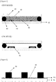
FIG. 1 is a view schematically illustrating a variable transmittance film in the related art. -
FIG. 2 is a view schematically illustrating a black partition wall pattern film according to an exemplary embodiment of the present application. -
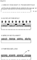
FIG. 3 is a view schematically illustrating a method of manufacturing the black partition wall pattern film according to the exemplary embodiment of the present application. -
FIG. 4 is a view schematically illustrating a method of manufacturing an imprinting mold according to the exemplary embodiment of the present application. -
FIG. 5 is a view illustrating a microscopic image, in a light transmitting mode, of the black partition wall pattern film according to the exemplary embodiment of the present application. -
FIG. 6 is a view illustrating an SEM image of the black partition wall pattern film according to the exemplary embodiment of the present application. -
- 10:
- First transparent substrate
- 20:
- Second transparent substrate
- 30:
- First electrode layer
- 40:
- Second electrode pattern
- 50:
- Negatively (-) charged carbon black nanoparticle
- 60:
- Ball spacer
- 70:
- Transparent substrate
- 80:
- Electrode layer
- 90:
- Black partition wall pattern
- 100:
- Black UV-curable resin layer
- 110:
- Black UV-curable resin composition
- 120:
- Imprinting mold
- 130:
- Transparent base
- 140:
- Dry film resist
- 150:
- Release layer
- Hereinafter, the present application will be described in detail.
- In the present application, the term "transparent" means that transmittance is about 80% or higher in a visible ray region (400 nm to 700 nm).
- Typically, it is essential to use a transparent electrode film and a metal pattern electrode film in order to manufacture an electrophoretic variable transmittance film. In addition, a cell gap needs to be maintained in order to inject an electrophoretic substance such as a negatively (-) charged carbon black particle dispersed solution between the two electrode films. To this end, a ball spacer, a column spacer pattern, or a partition wall pattern needs to be provided. A variable transmittance film in the related art is schematically illustrated in
FIG. 1 . - In a case in which a photolithography process using a photosensitive resin composition is applied to manufacture the partition wall pattern, there is a limitation in implementing a partition wall pattern having a uniform line width in a large area. This is due to uniformity of an exposure gap of a photomask and a photosensitive resin composition layer and uniformity of application of the photosensitive resin composition layer.
- In addition, in a case in which a transparent partition wall pattern is applied to manufacture the partition wall pattern, there may be a problem in that transmittance is increased in a light blocking mode when the exemplary embodiment is applied to a smart window. This problem may be caused by a leakage of light at the transparent partition wall pattern.
- In addition, in a case in which the photolithography process is used to manufacture a black partition wall pattern, exposure energy is not transferred to a lower side due to high optical density of a black photosensitive resin composition, and as a result, the partition wall pattern may not be implemented. In addition, in a case in which the exposure energy is excessively emitted in order to solve the problems, there may be a problem in that a line width of the partition wall pattern is greatly increased.
- Therefore, the present application provides a black partition wall pattern film and a method of manufacturing the same which are capable of solving the above-mentioned problems.
- A black partition wall pattern film according to an exemplary embodiment of the present application comprises: a transparent substrate; an electrode layer provided on the transparent substrate; a black partition wall pattern provided on the electrode layer; and a black UV-curable resin layer provided in a region on the electrode layer where no black partition wall pattern is provided.
- In the present application, the transparent substrate may be, but not limited to, a glass base or a transparent plastic base which is excellent in transparency, surface smoothness, tractability, and waterproofness, and the transparent base is not limited as long as the transparent base is typically used for electronic elements. Specifically, the transparent base may be made of glass; urethane resin; polyimide resin; polyester resin; (meth)acrylate-based polymeric resin; or polyolefin-based resin such as polyethylene or polypropylene.
- In the present application, the electrode layer may comprise a transparent conductive oxide. More specifically, the electrode layer may comprise, but not limited only to, one or more of an indium oxide, a zinc oxide, an indium tin oxide, an indium zinc oxide, and an indium zinc tin oxide.
- In order to ensure a redispersion property of charged particles when the light blocking mode is activated, surface resistance of the electrode layer may be 200 Ω/sq. or less.
- In the present application, a line height of the black partition wall pattern may be 5 µm or more, and a line width of the black partition wall pattern may be 30 µm or less. In addition, a line height of the black partition wall pattern may be 5 µm to 50 µm, and a line width of the black partition wall pattern may be 5 µm to 30 µm. If the line height of the black partition wall pattern is less than 5 µm, a distance between a transparent electrode and a metal electrode pattern substrate is decreased, such that the content of negatively (-) charged nanoparticles in a dispersion liquid is excessively increased in order to ensure the transmittance of 1% or less in the light blocking mode, and as a result, there may be a problem in that a dispersion property of the negatively (-) charged nanoparticles deteriorates when a variable transmittance element operates. In addition, if the line height of the black partition wall pattern is more than 50 µm, the distance between the transparent electrode and the metal electrode pattern substrate is increased, and as a result, an operating speed may be decreased. A cell gap between the electrodes may be determined based on the line height of the black partition wall pattern. More specifically, if the cell gap is small, concentration of a light blocking dispersion liquid may be increased in order to ensure a light blocking property, and an excessive increase in concentration of charged particles may degrade dispersion stability. In addition, if the cell gap is large, intensity of an electric field formed between the transparent electrode and the metal pattern may be decreased, and an electrophoretic property, that is, a movement speed of particles may be decreased as the distance between the charged particles and the metal pattern is increased.
- The transmittance of the black partition wall pattern may be 5% or less. In addition, the transmittance of the black partition wall pattern may be 0 to 5%. If the transmittance of the black partition wall pattern is more than 5%, there may be a problem in that the black partition wall pattern is visible in the light blocking mode. In the case of an electrophoretic variable transmittance film which is currently under development, the transmittance in the light blocking mode (a state in which a light blocking dispersion liquid is dispersed) is at a level of 1% to 5%. If the transmittance of the black partition wall pattern is higher than this level, a leakage of light may be visible at a partition wall part.
- A line spacing of the black partition wall pattern may be 100 µm to 1,000 µm. If the line spacing of the black partition wall pattern is less than 100 µm, a range of variable transmittance may be decreased due to an increase in area of a region of the partition wall pattern. If the line spacing of the black partition wall pattern is more than 1,000 µm, it may be difficult to maintain a uniform cell gap of the electrophoretic element. There is no variable transmittance in a region in which the black partition wall pattern is present, and as a result, an area of the variable transmittance region is decreased if the line spacing of the black partition wall pattern is too small when the line width remains the same. In contrast, if the line spacing is too large, a substrate (film) is deformed during a process of laminating a transparent electrode substrate and a metal pattern substrate, and as a result, bubbles may be produced, and uniformity of the cell gap may deteriorate.
- In the present application, a black UV-curable resin layer having a thickness equal to the line height of the black partition wall pattern is formed on an entire surface of a glass substrate, and then the transmittance may be measured by using a spectrophotometer (SolidSpec-3700, Shimadzu Corp.).
- In the present application, a thickness of the black UV-curable resin layer may be 1 µm or less, and transmittance of the black UV-curable resin layer may be 80% or more. In addition, the thickness of the black UV-curable resin layer may be more than 0 and 1 µm or less, and the transmittance of the black UV-curable resin layer may be 80% or more and less than 100%. If the thickness of the black UV-curable resin layer is more than 1 µm, the formation of the electric field between the transparent electrode and the metal electrode pattern is hindered, and as a result, there may be a problem in that an operating property of the electrophoretic element may deteriorate. In addition, if the transmittance of the black UV-curable resin layer is less than 80%, the transmittance is decreased in a light transmitting mode, and as a result, there may be a problem in that a variable transmittance range of the electrophoretic element is decreased.
- In the present application, the black partition wall pattern and the black UV-curable resin layer each may be made of a black UV-curable resin composition, and the black UV-curable resin composition may comprise, but not limited only to, one or more of an acrylic monomer, an acrylic oligomer, a photoinitiator, a black pigment, and a black dye.
- In the present application, the black partition wall pattern and the black UV-curable resin layer may be simultaneously formed by applying the black UV-curable resin composition onto the electrode layer and then performing an imprinting process. That is, the black partition wall pattern and the black UV-curable resin layer may comprise the same material.
- The black partition wall pattern film according to the exemplary embodiment of the present application is schematically illustrated in
FIG. 2 . As illustrated inFIG. 2 , the black partition wall pattern film according to the exemplary embodiment of the present application comprises: atransparent substrate 70; anelectrode layer 80 provided on thetransparent substrate 70; a blackpartition wall pattern 90 provided on theelectrode layer 80; and a black UV-curable resin layer 100 provided in a region on theelectrode layer 80 where no blackpartition wall pattern 90 is provided. - In addition, a method of manufacturing the black partition wall pattern film according to the exemplary embodiment of the present application comprises: forming an electrode layer on a transparent substrate; applying a black UV-curable resin composition on the electrode layer; pressing the applied black UV-curable resin composition with an imprinting mold and then curing the black UV-curable resin composition; and removing the imprinting mold.
- The method of manufacturing the black partition wall pattern film according to the exemplary embodiment of the present application is schematically illustrated in
FIG. 3 . As illustrated inFIG. 3 , the method of manufacturing the black partition wall pattern film according to the exemplary embodiment of the present application comprises: forming theelectrode layer 80 on thetransparent substrate 70; applying a black UV-curable resin composition 110 onto theelectrode layer 80; pressing the applied black UV-curable resin composition 110 with animprinting mold 120 and then curing the black UV-curable resin composition 110; and removing theimprinting mold 120. - In the present application, the forming of the electrode layer on the transparent substrate may use a method known in this technical field. More specifically, the forming of the electrode layer on the transparent substrate may use, but not limited only to, a deposition process or the like.
- A method of manufacturing the imprinting mold according to the exemplary embodiment of the present application is schematically illustrated in
FIG. 4 . More specifically, the imprinting mold may be manufactured by a manufacturing method comprising, but not limited only to, forming a dry film resist 140 on atransparent base 130; forming a pattern by exposing and developing the dry film resist 140; and forming arelease layer 150 on the transparent base and the pattern. - The release layer may be implemented as a layer with a mixture of fluorine-based and silicone-based release materials. A thickness of the release layer may be, but not limited only to, 100 nm or less. Examples of a method of forming the release layer comprise a wet coating method, a vapor deposition method, and the like, and the vapor deposition method is advantageous in implementing a uniform release layer on a surface having a stepped portion.
- In addition, the exemplary embodiment of the present application provides a variable transmittance film comprising the black partition wall pattern film.
- The variable transmittance film according to the exemplary embodiment of the present application may be formed by using a material and a method which are known in this technical field, except that the variable transmittance film comprises the black partition wall pattern film.
- For example, the variable transmittance film may have a second transparent substrate having a second electrode pattern provided on the black partition wall pattern film. Negatively (-) charged nanoparticles are comprised between the electrode layer and the second electrode pattern of the black partition wall pattern film.
- The negatively (-) charged nanoparticle may be, but not limited only to, a carbon black nanoparticle.
- The variable transmittance film may be manufactured by using, but not limited only to, a method of preparing the above-mentioned variable transmittance film, and then injecting a solution, in which the negatively (-) charged nanoparticles are dispersed, between the electrode layer and the second electrode pattern of the black partition wall pattern film.
- In the present application, the variable transmittance film may be operated by electrophoresis. The transmittance is decreased when the variable transmittance film according to the exemplary embodiment of the present application is in an OFF mode. The transmittance may be increased as the negatively (-) charged nanoparticles are concentrated on the metal pattern, which is a positive (+) electrode, due to the electrophoresis in an ON mode in which a voltage is applied to the electrode layer and the second electrode pattern.
- Hereinafter, the exemplary embodiment disclosed in the present specification will be described with reference to examples. However, the scope of the exemplary embodiment is not intended to be limited by the following examples.
- A dry film resist (DFR) having a thickness of 25 µm was roll-laminated on a transparent PET film of 250 µm under a condition in which a temperature was 110°C, a rate was 1.3 mpm (meter per min), and a pressure was 0.4 MPa. Exposure energy of 150 mJ/cm2 was selectively applied by using an exposure device using parallel light with a wavelength of 365 nm (photo process). A DFR pattern film having a debossed portion with a line width of 25 µm and a depth of 25 µm was manufactured by spray-developing the completely exposed DFR laminated film for 90 seconds by using a developer having Na2CO3 of 1 wt.% under a condition in which a temperature was 30°C and a spray pressure was 0.2 MPa.
- An imprinting mold was completely manufactured by forming a release layer having a thickness of 100 nm and having a mixture of fluorine-based and silicone-based release materials on the DFR pattern film by using a vapor deposition method.
- A transparent UV-curable resin composition was manufactured with compositions shown in Table 1.
[Table 1] Product Name Manufacturer Content (wt.%) CN9010 NS (alicyclic urethane acrylate monomer) Sartomer 28.5 CN8004 (alicyclic urethane acrylate monomer) Sartomer 28.5 SR444NS (pentaerythritol triacrylate) Sartomer 38 Irgacure 184 (photoinitiator) Ciba 4 SR9051 (attachment force enhancer) Sartomer 1 Sum 100 - A black UV-curable resin composition was manufactured by mixing a black mill base of 20 parts by weight (carbon black of 20 parts by weight having a particle diameter of 100 nm, a dispersing agent of 4 parts by weight, and trimethylol propane triacrylate of 76 parts by weight) with the transparent UV-curable resin composition of 80 parts by weight.
- The black UV-curable resin composition was applied onto an ITO film having surface resistance of 150 Q/sq., and then roll-pressed with the imprinting mold with a pressure of 0.5 MPa and a rate of 0.1 mpm. The ITO film having a black partition wall pattern was manufactured by irradiating the laminate, from above thereof, with exposure energy of 1 J/cm2 by using a UV curing device with a wavelength of 365 nm and then separating the imprinting mold from the ITO film.
- The black partition wall pattern manufactured by the imprinting process had a line width of 25 µm and a line height of 25 µm. A thickness of the black UV-curable resin layer in a region in which no black partition wall pattern is provided was 0.5 µm.
- The transmittance of the black partition wall pattern was 3%, and the transmittance of the black UV-curable resin layer having no black partition wall pattern was 92%.
- A black UV-curable resin layer having a thickness equal to a line height of the black partition wall pattern or the black UV-curable resin layer was formed on an entire surface of a glass substrate, and then the transmittance was measured by using a spectrophotometer (SolidSpec-3700, Shimadzu Corp.).
- A microscopic image, in the light transmitting mode, of the black partition wall pattern film according to Example 1 is illustrated in
FIG. 5 , and an SEM image of the black partition wall pattern film is illustrated inFIG. 6 . - A transparent UV-curable resin was applied onto an ITO film having surface resistance of 150 Ω/sq., and then roll-pressed with the imprinting mold with a pressure of 0.5 MPa and at a rate of 0.1 mpm. The ITO film having a transparent partition wall pattern was manufactured by irradiating the laminate, from above thereof, with exposure energy of 1 J/cm2 by using a UV curing device with a wavelength of 365 nm and then separating the imprinting mold from the ITO film.
- The transparent partition wall pattern manufactured by the imprinting process had a line width of 25 µm and a line height of 25 µm. A thickness of the transparent UV-curable resin layer in a region in which no transparent partition wall pattern is provided was 0.5 µm.
- The transmittance of the transparent partition wall pattern was 85%, and the transmittance of the transparent UV-curable resin layer having no transparent partition wall pattern was 95%.
- As a result, according to the exemplary embodiment of the present application, since the black partition wall pattern is comprised, it is possible to prevent the transmittance from increasing in the light blocking mode when the exemplary embodiment is applied to an electrophoretic smart window.
- In addition, according to the exemplary embodiment of the present application, since the black partition wall pattern film may be manufactured by using the imprinting process, it is possible to simplify the process of manufacturing the black partition wall pattern film and to form the black partition wall pattern having a desired line width.
Claims (12)
- A black partition wall pattern film comprising:a transparent substrate;an electrode layer provided on the transparent substrate;a black partition wall pattern provided on the electrode layer; anda black UV-curable resin layer provided in a region on the electrode layer where no black partition wall pattern is provided.
- The black partition wall pattern film of claim 1, wherein a line height of the black partition wall pattern is 5 µm or more.
- The black partition wall pattern film of claim 1, wherein a line width of the black partition wall pattern is 30 µm or less.
- The black partition wall pattern film of claim 1, wherein transmittance of the black partition wall pattern is 5% or less.
- The black partition wall pattern film of claim 1, wherein a thickness of the black UV-curable resin layer is 1 µm or less.
- The black partition wall pattern film of claim 1, wherein transmittance of the black UV-curable resin layer is 80% or more.
- The black partition wall pattern film of claim 1, wherein the black partition wall pattern and the black UV-curable resin layer comprise one or more of an acrylic monomer, an acrylic oligomer, a photoinitiator, a black pigment, and a black dye.
- The black partition wall pattern film of claim 1, wherein the electrode layer comprises a transparent conductive oxide.
- The black partition wall pattern film of claim 8, wherein the transparent conductive oxide comprises one or more of an indium oxide, a zinc oxide, an indium tin oxide, an indium zinc oxide, and an indium zinc tin oxide.
- A method of manufacturing the black partition wall pattern film according to any one of claims 1 to 9, the method comprising:forming an electrode layer on a transparent substrate;applying a black UV-curable resin composition onto the electrode layer;pressing the applied black UV-curable resin composition with an imprinting mold and then curing the black UV-curable resin composition; andremoving the imprinting mold.
- A variable transmittance film comprising the black partition wall pattern film according to any one of claims 1 to 9.
- The variable transmittance film of claim 11, wherein the variable transmittance film is operated by electrophoresis.
Applications Claiming Priority (2)
| Application Number | Priority Date | Filing Date | Title |
|---|---|---|---|
| KR1020180034975A KR102179729B1 (en) | 2018-03-27 | 2018-03-27 | Black partition wall pattern film and method for manufacturing thereof |
| PCT/KR2019/002784 WO2019190079A1 (en) | 2018-03-27 | 2019-03-11 | Black barrier wall pattern film and method for manufacturing same |
Publications (3)
| Publication Number | Publication Date |
|---|---|
| EP3779597A1 true EP3779597A1 (en) | 2021-02-17 |
| EP3779597A4 EP3779597A4 (en) | 2021-03-10 |
| EP3779597B1 EP3779597B1 (en) | 2024-10-16 |
Family
ID=68059313
Family Applications (1)
| Application Number | Title | Priority Date | Filing Date |
|---|---|---|---|
| EP19777058.9A Active EP3779597B1 (en) | 2018-03-27 | 2019-03-11 | Black barrier wall pattern film and method for manufacturing same |
Country Status (6)
| Country | Link |
|---|---|
| US (1) | US11709410B2 (en) |
| EP (1) | EP3779597B1 (en) |
| JP (1) | JP7305245B2 (en) |
| KR (1) | KR102179729B1 (en) |
| CN (1) | CN111279263A (en) |
| WO (1) | WO2019190079A1 (en) |
Family Cites Families (38)
| Publication number | Priority date | Publication date | Assignee | Title |
|---|---|---|---|---|
| JPH0949906A (en) | 1995-08-04 | 1997-02-18 | Toray Ind Inc | Black matrix substrate, microlens array sheet using the same, and manufacturing method thereof |
| JP2002542574A (en) | 1999-02-19 | 2002-12-10 | アムテック リサーチ インターナショナル エルエルシー | Conductive self-supporting microporous polymer sheet |
| JP2005321769A (en) | 2004-04-07 | 2005-11-17 | Bridgestone Corp | Information display panel |
| KR20050112940A (en) * | 2004-05-28 | 2005-12-01 | 삼성전자주식회사 | Hybrid mask mold having fake recession and method for fabrication of barrier ribs or etch barrier using the same |
| KR100790866B1 (en) | 2006-01-06 | 2008-01-03 | 삼성전자주식회사 | Black matrix for color filters and manufacturing method thereof |
| KR100741677B1 (en) * | 2006-03-06 | 2007-07-23 | 삼성전기주식회사 | Manufacturing method of substrate by imprinting |
| JP4710671B2 (en) | 2006-03-17 | 2011-06-29 | ブラザー工業株式会社 | Electrophoretic display medium and manufacturing method thereof |
| JP5236176B2 (en) * | 2006-11-17 | 2013-07-17 | 富士フイルム株式会社 | Black resin composition |
| KR20080049252A (en) | 2006-11-30 | 2008-06-04 | 엘지디스플레이 주식회사 | Color filter substrate and its manufacturing method |
| TW201032002A (en) | 2008-11-12 | 2010-09-01 | Sumitomo Chemical Co | Photosensitive black-colored resin composition, black matrix substrate, and manufacturing method of color filter |
| KR101363783B1 (en) | 2008-11-14 | 2014-02-17 | 엘지디스플레이 주식회사 | Method for forming an organic film on the photosensitive resin composition for imprinting and the substrate |
| US8503063B2 (en) | 2008-12-30 | 2013-08-06 | Sipix Imaging, Inc. | Multicolor display architecture using enhanced dark state |
| KR101590056B1 (en) | 2008-12-31 | 2016-01-29 | 주식회사 동진쎄미켐 | Manufacturing method of electric field driving display device |
| JP2010197649A (en) | 2009-02-25 | 2010-09-09 | Fuji Xerox Co Ltd | Image display medium and image display device |
| JP2010204540A (en) | 2009-03-05 | 2010-09-16 | Asahi Kasei E-Materials Corp | Electrophoretic display device |
| JP5410839B2 (en) | 2009-05-22 | 2014-02-05 | Hoya株式会社 | Multi-tone photomask manufacturing method, multi-tone photomask, and pattern transfer method |
| JP2011215197A (en) | 2010-03-31 | 2011-10-27 | Hoya Corp | Photomask and method for manufacturing the same |
| JP5597039B2 (en) * | 2010-06-23 | 2014-10-01 | キヤノン株式会社 | Radiation imaging apparatus, radiation imaging system, and method of manufacturing radiation imaging apparatus |
| KR101222488B1 (en) * | 2010-06-29 | 2013-01-16 | 한국기계연구원 | Method and flexible face for inorganic el display |
| KR101338999B1 (en) * | 2010-10-01 | 2013-12-09 | 엘지디스플레이 주식회사 | Electrophoretic display device and method of fabricating thereof |
| US8681415B2 (en) | 2010-07-14 | 2014-03-25 | Lg Display Co., Ltd. | Electrophoretic display device and fabrication method thereof |
| JP2012078547A (en) | 2010-10-01 | 2012-04-19 | Bridgestone Corp | Manufacturing method of information display panel and information display panel |
| KR20130020313A (en) | 2011-08-19 | 2013-02-27 | 삼성전기주식회사 | Touch sensor and method for manufacturing the same |
| JP5900233B2 (en) * | 2012-08-08 | 2016-04-06 | 日立化成株式会社 | Light control element, light control device, and driving method thereof |
| CN103293793B (en) * | 2013-05-31 | 2016-06-01 | 京东方科技集团股份有限公司 | A kind of double face display panel and manufacture method thereof |
| KR102168213B1 (en) | 2013-07-31 | 2020-10-21 | 주식회사 나노브릭 | Method for enhancing optical property of electrophoretic display |
| KR20150062240A (en) | 2013-11-28 | 2015-06-08 | (주)엘지하우시스 | Transmissivity-changeable film and method of manufacturing the same |
| JP2016148795A (en) | 2015-02-13 | 2016-08-18 | セイコーエプソン株式会社 | Electrophoretic display device, electrophoretic display device manufacturing method, and electronic apparatus |
| KR102318870B1 (en) * | 2015-03-10 | 2021-10-29 | 삼성디스플레이 주식회사 | Liquid crystal display device |
| CN106873209B (en) | 2015-09-30 | 2021-05-11 | 乐金显示有限公司 | Light control device, transparent display device including the same, and manufacturing method thereof |
| KR102367832B1 (en) * | 2015-09-30 | 2022-02-24 | 엘지디스플레이 주식회사 | Light controlling device, transparent display device including the same, and method for fabricating the same |
| KR102438632B1 (en) * | 2015-12-30 | 2022-08-31 | 엘지디스플레이 주식회사 | Display device and manufacturing method of display device |
| KR102040468B1 (en) * | 2016-01-26 | 2019-11-05 | 주식회사 엘지화학 | Method for manufacturing optical element |
| CN105549258B (en) | 2016-02-18 | 2019-02-01 | 武汉华星光电技术有限公司 | Color filter substrate and manufacturing method thereof |
| KR20180034975A (en) | 2016-09-28 | 2018-04-05 | 송연재 | Functional Mid-sole and Shoes including the same |
| CN110709761B (en) * | 2017-05-31 | 2022-06-28 | 夏普株式会社 | Liquid crystal display panel and liquid crystal display device |
| JP6789196B2 (en) * | 2017-09-08 | 2020-11-25 | 株式会社Joled | Manufacturing method of organic EL display panel and organic EL display panel |
| GB2571921A (en) * | 2018-03-05 | 2019-09-18 | Flexenable Ltd | Displays |
-
2018
- 2018-03-27 KR KR1020180034975A patent/KR102179729B1/en active Active
-
2019
- 2019-03-11 WO PCT/KR2019/002784 patent/WO2019190079A1/en not_active Ceased
- 2019-03-11 JP JP2020526185A patent/JP7305245B2/en active Active
- 2019-03-11 CN CN201980005327.9A patent/CN111279263A/en active Pending
- 2019-03-11 US US16/762,609 patent/US11709410B2/en active Active
- 2019-03-11 EP EP19777058.9A patent/EP3779597B1/en active Active
Also Published As
| Publication number | Publication date |
|---|---|
| WO2019190079A1 (en) | 2019-10-03 |
| US20200272016A1 (en) | 2020-08-27 |
| JP2021502610A (en) | 2021-01-28 |
| US11709410B2 (en) | 2023-07-25 |
| CN111279263A (en) | 2020-06-12 |
| EP3779597B1 (en) | 2024-10-16 |
| KR20190112957A (en) | 2019-10-08 |
| KR102179729B1 (en) | 2020-11-17 |
| EP3779597A4 (en) | 2021-03-10 |
| JP7305245B2 (en) | 2023-07-10 |
Similar Documents
| Publication | Publication Date | Title |
|---|---|---|
| CN105116604B (en) | Quantum dot display device and preparation method thereof | |
| US20030087087A1 (en) | Anti-static hard coat film and method of manufacturing the same | |
| JP2017207776A (en) | Display panel with pre-patterned images | |
| TWI614660B (en) | Transparent conductive film and touch panel therewith and display device | |
| CN1363056A (en) | Improved electrophoretic display and its novel manufacturing method | |
| TW200533962A (en) | Color filter | |
| KR102250382B1 (en) | Light transmission controllable film and smart window comprising the same | |
| EP3598219B1 (en) | Barrier rib pattern film and manufacturing method therefor | |
| EP3779597B1 (en) | Black barrier wall pattern film and method for manufacturing same | |
| KR20120046845A (en) | Liquid crystal display and fabricating method thereof | |
| JP4710671B2 (en) | Electrophoretic display medium and manufacturing method thereof | |
| CN115989445A (en) | Optical path control component and display device including the optical path control component | |
| US11966163B2 (en) | Photomask for imprinting and manufacturing method therefor | |
| Park et al. | Photolithographic process of microcapsule sheet for electrophoretic display | |
| KR102146539B1 (en) | Preparation method of substrate | |
| KR102391634B1 (en) | Display device having bezel pattern and method of manufacure the same | |
| JP3896761B2 (en) | Color filter manufacturing method and color filter | |
| KR102396509B1 (en) | Black partition wall pattern film and method for manufacturing thereof | |
| JP2010204540A (en) | Electrophoretic display device | |
| KR102868661B1 (en) | Light route control member and display having the same | |
| KR102872801B1 (en) | Light route control member and display having the same | |
| US11300875B2 (en) | Photoresist, display panel and display device | |
| CN101281261A (en) | Method for preparing anti-ultraviolet and anti-glare film and coating liquid thereof | |
| JP3128161B2 (en) | Manufacturing method of color filter | |
| JP2005250179A (en) | Photocurable resin composition for black matrix, method for producing substrate for liquid crystal display panel, black matrix and liquid crystal display panel |
Legal Events
| Date | Code | Title | Description |
|---|---|---|---|
| STAA | Information on the status of an ep patent application or granted ep patent |
Free format text: STATUS: THE INTERNATIONAL PUBLICATION HAS BEEN MADE |
|
| PUAI | Public reference made under article 153(3) epc to a published international application that has entered the european phase |
Free format text: ORIGINAL CODE: 0009012 |
|
| STAA | Information on the status of an ep patent application or granted ep patent |
Free format text: STATUS: REQUEST FOR EXAMINATION WAS MADE |
|
| 17P | Request for examination filed |
Effective date: 20200414 |
|
| AK | Designated contracting states |
Kind code of ref document: A1 Designated state(s): AL AT BE BG CH CY CZ DE DK EE ES FI FR GB GR HR HU IE IS IT LI LT LU LV MC MK MT NL NO PL PT RO RS SE SI SK SM TR |
|
| AX | Request for extension of the european patent |
Extension state: BA ME |
|
| A4 | Supplementary search report drawn up and despatched |
Effective date: 20210209 |
|
| RIC1 | Information provided on ipc code assigned before grant |
Ipc: G03F 7/16 20060101AFI20210203BHEP Ipc: G03F 7/00 20060101ALI20210203BHEP Ipc: G02F 1/167 20190101ALI20210203BHEP Ipc: G03F 7/20 20060101ALI20210203BHEP Ipc: G02F 1/1681 20190101ALI20210203BHEP |
|
| DAV | Request for validation of the european patent (deleted) | ||
| DAX | Request for extension of the european patent (deleted) | ||
| STAA | Information on the status of an ep patent application or granted ep patent |
Free format text: STATUS: EXAMINATION IS IN PROGRESS |
|
| 17Q | First examination report despatched |
Effective date: 20220202 |
|
| GRAP | Despatch of communication of intention to grant a patent |
Free format text: ORIGINAL CODE: EPIDOSNIGR1 |
|
| STAA | Information on the status of an ep patent application or granted ep patent |
Free format text: STATUS: GRANT OF PATENT IS INTENDED |
|
| INTG | Intention to grant announced |
Effective date: 20240730 |
|
| GRAS | Grant fee paid |
Free format text: ORIGINAL CODE: EPIDOSNIGR3 |
|
| GRAA | (expected) grant |
Free format text: ORIGINAL CODE: 0009210 |
|
| STAA | Information on the status of an ep patent application or granted ep patent |
Free format text: STATUS: THE PATENT HAS BEEN GRANTED |
|
| AK | Designated contracting states |
Kind code of ref document: B1 Designated state(s): AL AT BE BG CH CY CZ DE DK EE ES FI FR GB GR HR HU IE IS IT LI LT LU LV MC MK MT NL NO PL PT RO RS SE SI SK SM TR |
|
| REG | Reference to a national code |
Ref country code: GB Ref legal event code: FG4D |
|
| REG | Reference to a national code |
Ref country code: CH Ref legal event code: EP |
|
| REG | Reference to a national code |
Ref country code: IE Ref legal event code: FG4D |
|
| REG | Reference to a national code |
Ref country code: DE Ref legal event code: R096 Ref document number: 602019060527 Country of ref document: DE |
|
| REG | Reference to a national code |
Ref country code: LT Ref legal event code: MG9D |
|
| REG | Reference to a national code |
Ref country code: NL Ref legal event code: MP Effective date: 20241016 |
|
| REG | Reference to a national code |
Ref country code: AT Ref legal event code: MK05 Ref document number: 1733396 Country of ref document: AT Kind code of ref document: T Effective date: 20241016 |
|
| PG25 | Lapsed in a contracting state [announced via postgrant information from national office to epo] |
Ref country code: NL Free format text: LAPSE BECAUSE OF FAILURE TO SUBMIT A TRANSLATION OF THE DESCRIPTION OR TO PAY THE FEE WITHIN THE PRESCRIBED TIME-LIMIT Effective date: 20241016 |
|
| PG25 | Lapsed in a contracting state [announced via postgrant information from national office to epo] |
Ref country code: NL Free format text: LAPSE BECAUSE OF FAILURE TO SUBMIT A TRANSLATION OF THE DESCRIPTION OR TO PAY THE FEE WITHIN THE PRESCRIBED TIME-LIMIT Effective date: 20241016 |
|
| PG25 | Lapsed in a contracting state [announced via postgrant information from national office to epo] |
Ref country code: PT Free format text: LAPSE BECAUSE OF FAILURE TO SUBMIT A TRANSLATION OF THE DESCRIPTION OR TO PAY THE FEE WITHIN THE PRESCRIBED TIME-LIMIT Effective date: 20250217 Ref country code: HR Free format text: LAPSE BECAUSE OF FAILURE TO SUBMIT A TRANSLATION OF THE DESCRIPTION OR TO PAY THE FEE WITHIN THE PRESCRIBED TIME-LIMIT Effective date: 20241016 Ref country code: IS Free format text: LAPSE BECAUSE OF FAILURE TO SUBMIT A TRANSLATION OF THE DESCRIPTION OR TO PAY THE FEE WITHIN THE PRESCRIBED TIME-LIMIT Effective date: 20250216 |
|
| PG25 | Lapsed in a contracting state [announced via postgrant information from national office to epo] |
Ref country code: FI Free format text: LAPSE BECAUSE OF FAILURE TO SUBMIT A TRANSLATION OF THE DESCRIPTION OR TO PAY THE FEE WITHIN THE PRESCRIBED TIME-LIMIT Effective date: 20241016 |
|
| PG25 | Lapsed in a contracting state [announced via postgrant information from national office to epo] |
Ref country code: BG Free format text: LAPSE BECAUSE OF FAILURE TO SUBMIT A TRANSLATION OF THE DESCRIPTION OR TO PAY THE FEE WITHIN THE PRESCRIBED TIME-LIMIT Effective date: 20241016 |
|
| PG25 | Lapsed in a contracting state [announced via postgrant information from national office to epo] |
Ref country code: ES Free format text: LAPSE BECAUSE OF FAILURE TO SUBMIT A TRANSLATION OF THE DESCRIPTION OR TO PAY THE FEE WITHIN THE PRESCRIBED TIME-LIMIT Effective date: 20241016 |
|
| PG25 | Lapsed in a contracting state [announced via postgrant information from national office to epo] |
Ref country code: NO Free format text: LAPSE BECAUSE OF FAILURE TO SUBMIT A TRANSLATION OF THE DESCRIPTION OR TO PAY THE FEE WITHIN THE PRESCRIBED TIME-LIMIT Effective date: 20250116 |
|
| PG25 | Lapsed in a contracting state [announced via postgrant information from national office to epo] |
Ref country code: GR Free format text: LAPSE BECAUSE OF FAILURE TO SUBMIT A TRANSLATION OF THE DESCRIPTION OR TO PAY THE FEE WITHIN THE PRESCRIBED TIME-LIMIT Effective date: 20250117 Ref country code: AT Free format text: LAPSE BECAUSE OF FAILURE TO SUBMIT A TRANSLATION OF THE DESCRIPTION OR TO PAY THE FEE WITHIN THE PRESCRIBED TIME-LIMIT Effective date: 20241016 Ref country code: LV Free format text: LAPSE BECAUSE OF FAILURE TO SUBMIT A TRANSLATION OF THE DESCRIPTION OR TO PAY THE FEE WITHIN THE PRESCRIBED TIME-LIMIT Effective date: 20241016 |
|
| PG25 | Lapsed in a contracting state [announced via postgrant information from national office to epo] |
Ref country code: PL Free format text: LAPSE BECAUSE OF FAILURE TO SUBMIT A TRANSLATION OF THE DESCRIPTION OR TO PAY THE FEE WITHIN THE PRESCRIBED TIME-LIMIT Effective date: 20241016 |
|
| PG25 | Lapsed in a contracting state [announced via postgrant information from national office to epo] |
Ref country code: RS Free format text: LAPSE BECAUSE OF FAILURE TO SUBMIT A TRANSLATION OF THE DESCRIPTION OR TO PAY THE FEE WITHIN THE PRESCRIBED TIME-LIMIT Effective date: 20250116 |
|
| PG25 | Lapsed in a contracting state [announced via postgrant information from national office to epo] |
Ref country code: SM Free format text: LAPSE BECAUSE OF FAILURE TO SUBMIT A TRANSLATION OF THE DESCRIPTION OR TO PAY THE FEE WITHIN THE PRESCRIBED TIME-LIMIT Effective date: 20241016 |
|
| PG25 | Lapsed in a contracting state [announced via postgrant information from national office to epo] |
Ref country code: DK Free format text: LAPSE BECAUSE OF FAILURE TO SUBMIT A TRANSLATION OF THE DESCRIPTION OR TO PAY THE FEE WITHIN THE PRESCRIBED TIME-LIMIT Effective date: 20241016 |
|
| REG | Reference to a national code |
Ref country code: DE Ref legal event code: R097 Ref document number: 602019060527 Country of ref document: DE |
|
| PG25 | Lapsed in a contracting state [announced via postgrant information from national office to epo] |
Ref country code: EE Free format text: LAPSE BECAUSE OF FAILURE TO SUBMIT A TRANSLATION OF THE DESCRIPTION OR TO PAY THE FEE WITHIN THE PRESCRIBED TIME-LIMIT Effective date: 20241016 |
|
| PG25 | Lapsed in a contracting state [announced via postgrant information from national office to epo] |
Ref country code: RO Free format text: LAPSE BECAUSE OF FAILURE TO SUBMIT A TRANSLATION OF THE DESCRIPTION OR TO PAY THE FEE WITHIN THE PRESCRIBED TIME-LIMIT Effective date: 20241016 |
|
| PG25 | Lapsed in a contracting state [announced via postgrant information from national office to epo] |
Ref country code: SK Free format text: LAPSE BECAUSE OF FAILURE TO SUBMIT A TRANSLATION OF THE DESCRIPTION OR TO PAY THE FEE WITHIN THE PRESCRIBED TIME-LIMIT Effective date: 20241016 |
|
| PG25 | Lapsed in a contracting state [announced via postgrant information from national office to epo] |
Ref country code: CZ Free format text: LAPSE BECAUSE OF FAILURE TO SUBMIT A TRANSLATION OF THE DESCRIPTION OR TO PAY THE FEE WITHIN THE PRESCRIBED TIME-LIMIT Effective date: 20241016 |
|
| PG25 | Lapsed in a contracting state [announced via postgrant information from national office to epo] |
Ref country code: IT Free format text: LAPSE BECAUSE OF FAILURE TO SUBMIT A TRANSLATION OF THE DESCRIPTION OR TO PAY THE FEE WITHIN THE PRESCRIBED TIME-LIMIT Effective date: 20241016 |
|
| PLBE | No opposition filed within time limit |
Free format text: ORIGINAL CODE: 0009261 |
|
| STAA | Information on the status of an ep patent application or granted ep patent |
Free format text: STATUS: NO OPPOSITION FILED WITHIN TIME LIMIT |
|
| PG25 | Lapsed in a contracting state [announced via postgrant information from national office to epo] |
Ref country code: SE Free format text: LAPSE BECAUSE OF FAILURE TO SUBMIT A TRANSLATION OF THE DESCRIPTION OR TO PAY THE FEE WITHIN THE PRESCRIBED TIME-LIMIT Effective date: 20241016 |
|
| 26N | No opposition filed |
Effective date: 20250717 |
|
| PG25 | Lapsed in a contracting state [announced via postgrant information from national office to epo] |
Ref country code: MC Free format text: LAPSE BECAUSE OF FAILURE TO SUBMIT A TRANSLATION OF THE DESCRIPTION OR TO PAY THE FEE WITHIN THE PRESCRIBED TIME-LIMIT Effective date: 20241016 |
|
| REG | Reference to a national code |
Ref country code: CH Ref legal event code: H13 Free format text: ST27 STATUS EVENT CODE: U-0-0-H10-H13 (AS PROVIDED BY THE NATIONAL OFFICE) Effective date: 20251023 |
|
| PG25 | Lapsed in a contracting state [announced via postgrant information from national office to epo] |
Ref country code: LU Free format text: LAPSE BECAUSE OF NON-PAYMENT OF DUE FEES Effective date: 20250311 |
|
| REG | Reference to a national code |
Ref country code: BE Ref legal event code: MM Effective date: 20250331 |
|
| PG25 | Lapsed in a contracting state [announced via postgrant information from national office to epo] |
Ref country code: BE Free format text: LAPSE BECAUSE OF NON-PAYMENT OF DUE FEES Effective date: 20250331 |
|
| PG25 | Lapsed in a contracting state [announced via postgrant information from national office to epo] |
Ref country code: CH Free format text: LAPSE BECAUSE OF NON-PAYMENT OF DUE FEES Effective date: 20250331 |
|
| PG25 | Lapsed in a contracting state [announced via postgrant information from national office to epo] |
Ref country code: IE Free format text: LAPSE BECAUSE OF NON-PAYMENT OF DUE FEES Effective date: 20250311 |
|
| PGFP | Annual fee paid to national office [announced via postgrant information from national office to epo] |
Ref country code: GB Payment date: 20260224 Year of fee payment: 8 |
|
| PGFP | Annual fee paid to national office [announced via postgrant information from national office to epo] |
Ref country code: DE Payment date: 20260220 Year of fee payment: 8 |
|
| PGFP | Annual fee paid to national office [announced via postgrant information from national office to epo] |
Ref country code: FR Payment date: 20260224 Year of fee payment: 8 |