EP3776602B1 - Wärmgeschütze varistorelement - Google Patents
Wärmgeschütze varistorelement Download PDFInfo
- Publication number
- EP3776602B1 EP3776602B1 EP19716127.6A EP19716127A EP3776602B1 EP 3776602 B1 EP3776602 B1 EP 3776602B1 EP 19716127 A EP19716127 A EP 19716127A EP 3776602 B1 EP3776602 B1 EP 3776602B1
- Authority
- EP
- European Patent Office
- Prior art keywords
- varistor
- contact element
- casing
- thermal
- protection device
- Prior art date
- Legal status (The legal status is an assumption and is not a legal conclusion. Google has not performed a legal analysis and makes no representation as to the accuracy of the status listed.)
- Active
Links
Images

Classifications
-
- H—ELECTRICITY
- H01—ELECTRIC ELEMENTS
- H01C—RESISTORS
- H01C7/00—Non-adjustable resistors formed as one or more layers or coatings; Non-adjustable resistors made from powdered conducting material or powdered semi-conducting material with or without insulating material
- H01C7/10—Non-adjustable resistors formed as one or more layers or coatings; Non-adjustable resistors made from powdered conducting material or powdered semi-conducting material with or without insulating material voltage responsive, i.e. varistors
-
- H—ELECTRICITY
- H01—ELECTRIC ELEMENTS
- H01C—RESISTORS
- H01C7/00—Non-adjustable resistors formed as one or more layers or coatings; Non-adjustable resistors made from powdered conducting material or powdered semi-conducting material with or without insulating material
- H01C7/10—Non-adjustable resistors formed as one or more layers or coatings; Non-adjustable resistors made from powdered conducting material or powdered semi-conducting material with or without insulating material voltage responsive, i.e. varistors
- H01C7/12—Overvoltage protection resistors; Arresters
-
- H—ELECTRICITY
- H01—ELECTRIC ELEMENTS
- H01C—RESISTORS
- H01C1/00—Details
- H01C1/02—Housing; Enclosing; Embedding; Filling the housing or enclosure
-
- H—ELECTRICITY
- H01—ELECTRIC ELEMENTS
- H01C—RESISTORS
- H01C1/00—Details
- H01C1/02—Housing; Enclosing; Embedding; Filling the housing or enclosure
- H01C1/022—Housing; Enclosing; Embedding; Filling the housing or enclosure the housing or enclosure being openable or separable from the resistive element
-
- H—ELECTRICITY
- H01—ELECTRIC ELEMENTS
- H01C—RESISTORS
- H01C1/00—Details
- H01C1/14—Terminals or tapping points specially adapted for resistors; Arrangements of terminals or tapping points on resistors
-
- H—ELECTRICITY
- H01—ELECTRIC ELEMENTS
- H01C—RESISTORS
- H01C1/00—Details
- H01C1/14—Terminals or tapping points specially adapted for resistors; Arrangements of terminals or tapping points on resistors
- H01C1/144—Terminals or tapping points specially adapted for resistors; Arrangements of terminals or tapping points on resistors the terminals or tapping points being welded or soldered
-
- H—ELECTRICITY
- H01—ELECTRIC ELEMENTS
- H01C—RESISTORS
- H01C7/00—Non-adjustable resistors formed as one or more layers or coatings; Non-adjustable resistors made from powdered conducting material or powdered semi-conducting material with or without insulating material
- H01C7/10—Non-adjustable resistors formed as one or more layers or coatings; Non-adjustable resistors made from powdered conducting material or powdered semi-conducting material with or without insulating material voltage responsive, i.e. varistors
- H01C7/12—Overvoltage protection resistors; Arresters
- H01C7/126—Means for protecting against excessive pressure or for disconnecting in case of failure
-
- H—ELECTRICITY
- H01—ELECTRIC ELEMENTS
- H01H—ELECTRIC SWITCHES; RELAYS; SELECTORS; EMERGENCY PROTECTIVE DEVICES
- H01H37/00—Thermally-actuated switches
- H01H37/74—Switches in which only the opening movement or only the closing movement of a contact is effected by heating or cooling
- H01H37/76—Contact member actuated by melting of fusible material, actuated due to burning of combustible material or due to explosion of explosive material
- H01H37/761—Contact member actuated by melting of fusible material, actuated due to burning of combustible material or due to explosion of explosive material with a fusible element forming part of the switched circuit
-
- H—ELECTRICITY
- H01—ELECTRIC ELEMENTS
- H01H—ELECTRIC SWITCHES; RELAYS; SELECTORS; EMERGENCY PROTECTIVE DEVICES
- H01H37/00—Thermally-actuated switches
- H01H37/74—Switches in which only the opening movement or only the closing movement of a contact is effected by heating or cooling
- H01H37/76—Contact member actuated by melting of fusible material, actuated due to burning of combustible material or due to explosion of explosive material
- H01H37/761—Contact member actuated by melting of fusible material, actuated due to burning of combustible material or due to explosion of explosive material with a fusible element forming part of the switched circuit
- H01H2037/762—Contact member actuated by melting of fusible material, actuated due to burning of combustible material or due to explosion of explosive material with a fusible element forming part of the switched circuit using a spring for opening the circuit when the fusible element melts
Definitions
- the invention concerns a thermal protection device to protect an electrical element against overheating, for example a varistor.
- a varistor is such an electrical element.
- the varistor can change from an electrically insulating state to an electrically conductive state with a characteristic current-voltage behaviour.
- the varistor can protect the electrical circuit.
- the varistor has to be protected in turn when the overvoltage persists and a high current flows through the varistor.
- US 6 323 750 B1 relates to an electrical component, in particular to a varistor, which is installed in a plastic cup and has at least two electrical connecting leads.
- WO 2017/140463 A1 refers to a varistor component comprising a first external contact and a second external contact.
- JP 2009 218508 A relates to a SPD (Surge Protection Device) with a separation mechanism.
- WO2007/142152 A1 relates to a SPD comprising a zinc oxide type varistor.
- the task is a thermal protection device to protect a varistor in cases of overheating due to a persistently high voltage applied to the varistor over a certain time.
- the invention relates to a thermal varistor protection device with a casing comprising an insulating material and a varistor which is embedded in the insulating material of the casing, wherein the varistor comprises a first metallization electrode, which is only partly covered by an insulating material of the casing to allow an electrically conductive connection to the first metallization electrode of the varistor. Furthermore the thermal varistor protection device comprises a first terminal wire that is electrically conductively connected to the first metallization electrode of the varistor.
- the thermal varistor protection device also comprises a contact element which is electrically conductively connected to the first metallization electrode of the varistor in a region where the varistor is not covered by the insulating material of the casing and wherein the contact element is pre-stressed to provide a fast separation of the contact element and the first metallization electrode if the electrical connection between the contact element and the first metallization electrode gets loose.
- the varistor is protected against environmental influences and is largely electrically insulated as a result of being embedded by the insulating material of the casing. Therefore the varistor is protected against unwanted contact. Since the first metallization electrode is only partly embedded in the insulating material of the casing, an electrically conductive connection is possible. The pre-stressed contact element ensures a fast and secure separation of contact element and first metallization electrode. Therefore an improvement in the protectional function is provided.
- the pre-stress of the contact element is caused by the contact element itself.
- the contact element comprises an elastic part, which causes the pre-stress during an existent connection between the contact element and the first metallization electrode of the varistor.
- the thermal varistor protection device can be built in smaller dimensions, since no additional feature is needed to generate the pre-stress.
- the casing provides a feature to hold the contact element in place. If the pre-stress to the connection element is caused by a part of the connection element, it is possible to use the feature to build up the pre-stress.
- the feature can be designed in the form of a rivet.
- the feature can comprise more than one rivet.
- Such a rivet can be part of the casing. In this case it would be possible to produce the rivet in one production step together with the casing itself. That would save production time and costs.
- the electrically conductive connection between the first metallization electrode of the embedded varistor and the contact element can be realized as a low-temperature solder joint.
- the low temperature would be a characteristic temperature at which the solder reaches a state where it would allow the pre-stress to interrupt the connection.
- the low temperature can be a characteristic temperature at which the solder becomes liquid.
- a value of the characteristic temperature of the low-temperature solder can be in a range from 100°C to 210°C. In a special embodiment the value of the characteristic temperature is 138°C.
- a thermally triggered interruption of a pre-stressed connection can be ensured.
- the triggering may be caused by a temperature increase of the varistor as well as by a high current which flows through the electrically conductive connection and heats it up. Both triggering mechanisms can be realized in the electrically conductive connection between the contact element and the first metallization electrode of the varistor, since the connection is close to the varistor and therefore shows a similar temperature behaviour, and the contact element and the connection are connected in series to the varistor and thus have the same current which flows through the varistor and which would heat up all the elements on the current path.
- the pre-stress of the contact element pushes the contact element away from the region where the metallization electrode of the varistor is free from insulating material of the casing.
- the contact element can be pushed in a region where the metallization electrode of the varistor is covered by the insulating material of the casing. Thereby the contact element can get pushed against a wall of the casing by the pre-stress.
- a local separation of contact element and metallization electrode can improve a save disconnection of those parts if the connection becomes loose.
- the separation by the pre-stress can lead to a fast separation, in addition.
- the first terminal wire can comprise a loop-like-shaped end which is electrically conductively connected to the first metallization electrode of the varistor. More specifically, the end can be shaped as an open loop or an open lug. This modification of the first terminal wire can increase a contact area between the first terminal wire and the metallization electrode of the varistor. As a result, the loop-like shape of the connected end of the first terminal wire can lead to an improved electrically conductive contact with higher stability and conductivity.
- the contact element is a wire.
- the contact element can comprise an end which is electrically conductively connected to the metallization electrode of the varistor.
- the thermal varistor protection device can comprise a cap.
- the cap can be designed to be removably placed on the casing.
- the casing can define a cavity which is closed by the cap.
- Such a cavity would protect inner parts against environmental influences.
- the set of parts in the cavity can comprise the region on the metallization electrode of the varistor which is free from insulating material of the casing, a part of the contact element, the feature to hold the contact element, and the electrically conductive connection between the contact element and the metallization electrode of the varistor.
- a general shape of the casing can be adjusted to the shape of the varistor. Therefore the casing can have a generally cuboid shape. An alteration of the casing can reduce the needed material to embed the varistor and therefore reduce costs.
- the thermal varistor protection device can comprise a second terminal wire.
- the second terminal wire would be electrically conductively connected to a second metallization electrode of the varistor. Furthermore an arrangement of the second metallization electrode on the varistor at an opposite side to the first metallization electrode is possible.
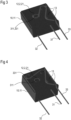
- FIG. 1 gives a perspective view on an embodiment of a thermal varistor protection 1.
- a casing 10 is made from insulating material 11 and is represented transparent.
- a varistor 2 is embedded and is partly covered by the insulating material 11.
- the varistor 2 can be accessed for establishing an electrically conductive connection.
- the thermal varistor protection 1 comprises a cap 19 to cover a cavity in the casing 10 and to protect parts from environmental influences.
- a first terminal wire 31 and a second terminal wire 32 are electrically conductively connected to opposite sides of the varistor 2 and protrude from the casing 10.
- a contact element is electrically conductively connected to the varistor 2 in a region 12 which is free of the insulating material 11, and protrudes from the casing 10, too.
- the first terminal wire 31 and the contact element 33 are adjacent to one another and connected to the same side of the varistor 2 in the region 12 which is free of insulating material 11. Both the first terminal wire 31 and the contact element 33 have an open loop 311,331 at their respective ends connected to the varistor.
- FIG. 2 shows a possible embodiment of a varistor 2 that would be the object of protection in a thermal varistor protection 1 of this invention.
- the varistor 2 comprises a first metallization electrode 21, on which a first terminal wire 31 is electrically conductively connected. Furthermore, the varistor 2 of the shown embodiment has a second metallization electrode 22 (not visible) on the opposite side of the first metallization electrode 21. There is a second terminal wire 32, which is electrically conductively connected to the second metallization electrode 22 of the varistor 2.
- a terminal wire that is connected to the varistor 2 can comprise an open loop at the connected end.
- the first terminal wire 31 shows an open loop 311 at its connected end.
- the cuboid-like shape of the varistor is an example only.
- a cylinder-like shape or other shapes are also possible for an embodiment of the protected varistor 2.
- FIG. 3 shows a schematic perspective of an embodiment of the thermal varistor protection 1 without a cap 19.
- a varistor 2 is embedded in a casing 10 of insulating material 11 .
- a first terminal wire 31 and a second terminal wire 32 are electrically conductively connected to two metallization electrodes on opposite sides of the varistor 2 and protrude out of the casing 10.
- the contact element 33 is electrically conductively connected to a metallization electrode 21 of the varistor adjacent to the point of connection of the first terminal wire 31, which is in a region 12 where the varistor 2 is free from insulating material 11.
- the casing 10 comprises features 13 to hold the contact element 33 and build up a pre-stress in the contact element 33.
- the contact element 33 is elastic to build up the pre-stress.
- the connection between the metallization electrode 21 of the varistor 2 and the contact element 33 can be realized with a low-temperature solder.
- the varistor 2 changes from an electrically insulating state to an electrically conductive state, and a high current flows through the varistor 2 and the connections at the varistor 2. If a high electrical current flows through a solder joint of a low-temperature solder, the solder gets heated up and becomes liquid. If the low-temperature solder in the connection between the metallization electrode 21 of the varistor 2 and the contact element 33 becomes liquid, the contact element 33 gets pushed away from the region 12 without insulating material 11 due to its inner pre-stress caused by the features 13 of the casing 10.
- Figure 4 shows a case where the connection between a contact element 33 and the metallization electrode 21 of a varistor 2 embedded in the casing 10 has become loose. Due to the inner pre-stress of the contact element 33 and the loosened connection, the contact element 33 is pushed to a wall of a cavity in the casing 10 and away from a region 12 where the varistor 2 is free from electrically insulating material 11. The inner pre-stress of the contact element 33 is caused by a feature 13 of the casing 10 that has the additional function to hold the contact element 33 in its position, even if the connection to the metallization electrode 21 of the varistor 2 is undone.
- Both the terminal wire 31 and the contact element 33 have an open loop 311,331 at their respective ends which are supposed to be electrically conductively connected to the metallization electrode 21 of the varistor 2.
- the electrically conductive connection between the contact element 33 and the metallization electrode 21 of the varistor 2 can be realized with a low-temperature solder. If the low-temperature solder becomes liquid due to a high current that is caused by a high voltage which makes the varistor 2 switch from an electrically insulating state to an electrically conductive state, the inner pre-stress of the terminal 33 pushes the end with the open loop 331 against a wall of the cavity of the casing 10.
Landscapes
- Engineering & Computer Science (AREA)
- Microelectronics & Electronic Packaging (AREA)
- Physics & Mathematics (AREA)
- Electromagnetism (AREA)
- Chemical & Material Sciences (AREA)
- Combustion & Propulsion (AREA)
- Thermistors And Varistors (AREA)
Claims (10)
- Thermische Varistor-Schutzvorrichtung (1), die umfasst- ein Gehäuse (10), das ein Isoliermaterial (11) umfasst,- einen Varistor (2), der in das Isoliermaterial (11) des Gehäuses (10) eingebettet ist, wobei der Varistor (2) eine erste Metallisierungselektrode (21) umfasst, die nur teilweise von dem Isoliermaterial (11) des Gehäuses (10) bedeckt ist, um eine elektrisch leitende Verbindung zu ermöglichen,- einen ersten Anschlussdraht (31), der mit der ersten Metallisierungselektrode (21) des Varistors (2) elektrisch leitend verbunden ist,- ein Kontaktelement (33), das mit der ersten Metallisierungselektrode (21) des Varistors (2) in einem Bereich (12), in dem der Varistor nicht von dem Isoliermaterial (11) des Gehäuses (10) bedeckt ist, elektrisch leitend verbunden ist, und- wobei das Kontaktelement (33) vorbelastet ist, um eine schnelle Trennung des Kontaktelements (33) und der ersten Metallisierungselektrode (21) sicherzustellen, wenn die elektrisch leitende Verbindung zwischen dem Kontaktelement (33) und der ersten Elektrode (21) lose wird,- wobei die Vorbelastung des Kontaktelements (33) durch einen Teil des Kontaktelements (33) selbst verursacht wird und daher ein Teil des Kontaktelements (33) elastisch ist und- wobei das Gehäuse (10) ein Element (13) zum Halten des Kontaktelements (33) an Ort und Stelle und zum Aufbauen der Vorbelastung in dem elastischen Teil des Kontaktelements (33) aufweist.
- Thermische Varistor-Schutzvorrichtung (1) nach Anspruch 1, wobei die elektrisch leitende Verbindung zwischen der ersten Metallisierungselektrode (21) des Varistors (2) und dem Kontaktelement (33) als Niedertemperatur-Lötverbindung ausgeführt ist, wobei die Niedertemperatur eine charakteristische Temperatur ist, bei der die Lötverbindung einen Zustand erreicht, in dem sie zulässt, dass die Vorbelastung den Kontakt unterbricht.
- Thermische Varistor-Schutzvorrichtung (1) nach Anspruch 1, wobei die charakteristische Temperatur die Schmelztemperatur des Lots ist, die in einem Bereich von 100 °C bis 210 °C liegt, z. B. 138 °C.
- Thermische Varistor-Schutzvorrichtung (1) nach einem der vorhergehenden Ansprüche, wobei das Element (13) zum Halten des Kontaktelements (33) an Ort und Stelle und zum Aufbauen der Vorbelastung in dem Kontaktelement (33) in Form von Nieten ausgebildet ist.
- Thermische Varistor-Schutzvorrichtung (1) nach einem der vorhergehenden Ansprüche, wobei die Vorbelastung des Kontaktelements (33) das Kontaktelement (33) gegen eine Wand des Gehäuses (10) weg von dem Bereich (12), in dem der Varistor (2) nicht von dem Isoliermaterial (11) des Gehäuses (10) bedeckt ist, drückt, wenn die Verbindung zu der ersten Metallisierungselektrode (21) des Varistors (2) lose wird.
- Thermische Varistor-Schutzvorrichtung (1) nach einem der vorhergehenden Ansprüche, wobei der erste Anschlussdraht (31) an dem Ende eine offene Schlaufe (311) aufweist, die mit der ersten Metallisierungselektrode (21) des Varistors (2) elektrisch leitend verbunden ist, um die Kontaktfläche zu vergrößern.
- Thermische Varistor-Schutzvorrichtung (1) nach einem der vorhergehenden Ansprüche, wobei das Kontaktelement (33) an einem Ende eine offene Schlaufe (331) aufweist, die dazu ausgelegt ist, mit der ersten Metallisierungselektrode (21) des Varistors (2) elektrisch leitend verbunden zu werden, um die Kontaktfläche zu vergrößern.
- Thermische Varistor-Schutzvorrichtung (1) nach einem der vorhergehenden Ansprüche, wobei das Gehäuse (10) einen Hohlraum definiert, der durch eine Kappe (19) verschlossen ist, um die inneren Teile vor Umwelteinflüssen zu schützen.
- Thermische Varistor-Schutzvorrichtung (1) nach einem der vorhergehenden Ansprüche, wobei das Gehäuse (10) im Allgemeinen quaderförmig ist.
- Thermische Varistor-Schutzvorrichtung (1) nach einem der vorhergehenden Ansprüche, die einen zweiten Anschlussdraht (32) umfasst, der mit einer zweiten Metallisierungselektrode (22) des Varistors (2) elektrisch leitend verbunden ist.
Applications Claiming Priority (2)
| Application Number | Priority Date | Filing Date | Title |
|---|---|---|---|
| CN201810300480.1A CN110349719A (zh) | 2018-04-04 | 2018-04-04 | 压敏电阻器热保护装置 |
| PCT/EP2019/058408 WO2019193055A1 (en) | 2018-04-04 | 2019-04-03 | Thermal protected varistor device |
Publications (2)
| Publication Number | Publication Date |
|---|---|
| EP3776602A1 EP3776602A1 (de) | 2021-02-17 |
| EP3776602B1 true EP3776602B1 (de) | 2025-05-28 |
Family
ID=66092334
Family Applications (1)
| Application Number | Title | Priority Date | Filing Date |
|---|---|---|---|
| EP19716127.6A Active EP3776602B1 (de) | 2018-04-04 | 2019-04-03 | Wärmgeschütze varistorelement |
Country Status (5)
| Country | Link |
|---|---|
| US (1) | US11605482B2 (de) |
| EP (1) | EP3776602B1 (de) |
| CN (2) | CN116052967A (de) |
| TW (2) | TWI805729B (de) |
| WO (1) | WO2019193055A1 (de) |
Families Citing this family (1)
| Publication number | Priority date | Publication date | Assignee | Title |
|---|---|---|---|---|
| CN117894535A (zh) * | 2022-10-14 | 2024-04-16 | 东莞令特电子有限公司 | 热保护金属氧化物压敏电阻 |
Family Cites Families (20)
| Publication number | Priority date | Publication date | Assignee | Title |
|---|---|---|---|---|
| US2770390A (en) * | 1952-06-20 | 1956-11-13 | Protectoseal Co | Safety container |
| DE19717634C2 (de) * | 1997-04-25 | 2000-06-08 | Epcos Ag | Elektrisches Bauelement mit Sicherheitstrennvorrichtung |
| US6430019B1 (en) * | 1998-06-08 | 2002-08-06 | Ferraz S.A. | Circuit protection device |
| DE19952888A1 (de) * | 1999-11-03 | 2001-05-10 | Abb Cmc Carl Maier Ag Schaffha | Thermisch auslösbare Schaltstelle |
| CN2535906Y (zh) * | 2002-04-01 | 2003-02-12 | 李炬 | 热保护型压敏电阻器 |
| CN2645314Y (zh) * | 2003-09-18 | 2004-09-29 | 成都凯瑞达电子技术有限公司 | 浪涌保护组件 |
| CN100373727C (zh) * | 2004-08-20 | 2008-03-05 | 四川康姆逊电磁防护有限责任公司 | 一种过热过电压保护器 |
| CN100561611C (zh) | 2005-09-03 | 2009-11-18 | 徐忠厚 | 设有合金型温度保险丝的压敏电阻 |
| CN100533605C (zh) * | 2006-03-03 | 2009-08-26 | 隆科电子(惠阳)有限公司 | 具有超温脱离机构和压敏电阻器的总成 |
| JP2007324535A (ja) * | 2006-06-05 | 2007-12-13 | Otowa Denki Kogyo Kk | 切り離し機構付spd |
| JP5278846B2 (ja) * | 2008-03-12 | 2013-09-04 | 音羽電機工業株式会社 | 切り離し機構付spd |
| US8031456B2 (en) * | 2009-05-12 | 2011-10-04 | Ceramate Technical Co., Ltd. | Explosion-roof and flameproof pullout safety surge absorbing module |
| CN203026939U (zh) * | 2013-01-14 | 2013-06-26 | 贵阳高新益舸电子有限公司 | 新型浪涌保护器 |
| CN203070854U (zh) * | 2013-01-22 | 2013-07-17 | 隆科电子(惠阳)有限公司 | 具有安装保护功能窗口的压敏电阻 |
| DE102013011646A1 (de) * | 2013-07-11 | 2015-01-15 | Pero Nilovic | Thermoschutz für einen Varistor |
| TWI545605B (zh) | 2013-12-13 | 2016-08-11 | 勝德國際研發股份有限公司 | 整合式突波吸收裝置 |
| CN103943292B (zh) * | 2014-04-04 | 2016-08-24 | 广西新未来信息产业股份有限公司 | 一种带热脱扣指示功能的安全型压敏电阻器 |
| WO2017139912A1 (en) * | 2016-02-15 | 2017-08-24 | Dongguan Littelfuse Electronics, Co., Ltd. | Thermal metal oxide varistor circuit protection device |
| DE102016102968A1 (de) * | 2016-02-19 | 2017-08-24 | Epcos Ag | Varistor-Komponente und Verfahren zum Sichern einer Varistor-Komponente |
| CN110024054B (zh) * | 2017-10-13 | 2021-06-29 | 东莞令特电子有限公司 | 热保护金属氧化物压敏电阻器 |
-
2018
- 2018-04-04 CN CN202211705078.4A patent/CN116052967A/zh active Pending
- 2018-04-04 CN CN201810300480.1A patent/CN110349719A/zh active Pending
-
2019
- 2019-04-03 TW TW108112240A patent/TWI805729B/zh active
- 2019-04-03 EP EP19716127.6A patent/EP3776602B1/de active Active
- 2019-04-03 WO PCT/EP2019/058408 patent/WO2019193055A1/en not_active Ceased
- 2019-04-03 US US17/040,901 patent/US11605482B2/en active Active
- 2019-04-03 TW TW112118768A patent/TWI855695B/zh active
Also Published As
| Publication number | Publication date |
|---|---|
| CN110349719A (zh) | 2019-10-18 |
| TW202347365A (zh) | 2023-12-01 |
| WO2019193055A1 (en) | 2019-10-10 |
| EP3776602A1 (de) | 2021-02-17 |
| US20210012933A1 (en) | 2021-01-14 |
| CN116052967A (zh) | 2023-05-02 |
| TW201942921A (zh) | 2019-11-01 |
| TWI805729B (zh) | 2023-06-21 |
| TWI855695B (zh) | 2024-09-11 |
| US11605482B2 (en) | 2023-03-14 |
Similar Documents
| Publication | Publication Date | Title |
|---|---|---|
| CN103069670B (zh) | 热过载保护装置 | |
| US20140232512A1 (en) | Thermal metal oxide varistor circuit protection device | |
| CN103098165B (zh) | 过热保护装置 | |
| US20100219929A1 (en) | Thermal fuse with current fuse function | |
| CN104798168A (zh) | 具有过电流阻断功能及电涌吸收功能的复合防护部件 | |
| US20170110279A1 (en) | Thermal metal oxide varistor circuit protection device | |
| CN104025243A (zh) | 具有过电流阻断功能的自复型保险丝 | |
| US9378910B2 (en) | Thermal cut-off device | |
| WO2014171515A1 (ja) | 保護装置 | |
| KR20160046856A (ko) | 보호 장치 | |
| US20200279701A1 (en) | Thermal Metal Oxide Varistor Circuit Protection Device | |
| KR101220283B1 (ko) | 대전류용 반복형 퓨즈 | |
| EP3776603B1 (de) | Wärmgeschütze varistorelement | |
| US11605482B2 (en) | Thermal protected varistor device | |
| US9887057B2 (en) | Remote activated fuse and circuit | |
| CN109961990B (zh) | 一种保护元件及保护模块 | |
| US20120223803A1 (en) | Thermal overload protection apparatus | |
| CN204189712U (zh) | 一种电路保护装置 | |
| CN106463303A (zh) | 保护装置 | |
| KR101504132B1 (ko) | 복합보호소자 | |
| US20250157770A1 (en) | Breaker assembly | |
| KR20150115356A (ko) | 정특성 서미스터를 이용한 안전장치 | |
| JP2002015902A (ja) | 保護素子 | |
| JP2000209768A (ja) | 過熱及び過電流阻止ユニット |
Legal Events
| Date | Code | Title | Description |
|---|---|---|---|
| STAA | Information on the status of an ep patent application or granted ep patent |
Free format text: STATUS: UNKNOWN |
|
| STAA | Information on the status of an ep patent application or granted ep patent |
Free format text: STATUS: THE INTERNATIONAL PUBLICATION HAS BEEN MADE |
|
| PUAI | Public reference made under article 153(3) epc to a published international application that has entered the european phase |
Free format text: ORIGINAL CODE: 0009012 |
|
| STAA | Information on the status of an ep patent application or granted ep patent |
Free format text: STATUS: REQUEST FOR EXAMINATION WAS MADE |
|
| 17P | Request for examination filed |
Effective date: 20200903 |
|
| AK | Designated contracting states |
Kind code of ref document: A1 Designated state(s): AL AT BE BG CH CY CZ DE DK EE ES FI FR GB GR HR HU IE IS IT LI LT LU LV MC MK MT NL NO PL PT RO RS SE SI SK SM TR |
|
| AX | Request for extension of the european patent |
Extension state: BA ME |
|
| DAV | Request for validation of the european patent (deleted) | ||
| DAX | Request for extension of the european patent (deleted) | ||
| RIN1 | Information on inventor provided before grant (corrected) |
Inventor name: HE, ZHOUQUAN Inventor name: SU, ZILONG Inventor name: ZHANG, RONGGUANG Inventor name: TIAN, XIAOJIA Inventor name: YANG, WEN |
|
| GRAP | Despatch of communication of intention to grant a patent |
Free format text: ORIGINAL CODE: EPIDOSNIGR1 |
|
| STAA | Information on the status of an ep patent application or granted ep patent |
Free format text: STATUS: GRANT OF PATENT IS INTENDED |
|
| INTG | Intention to grant announced |
Effective date: 20241213 |
|
| GRAS | Grant fee paid |
Free format text: ORIGINAL CODE: EPIDOSNIGR3 |
|
| P01 | Opt-out of the competence of the unified patent court (upc) registered |
Free format text: CASE NUMBER: APP_10849/2025 Effective date: 20250305 |
|
| GRAA | (expected) grant |
Free format text: ORIGINAL CODE: 0009210 |
|
| STAA | Information on the status of an ep patent application or granted ep patent |
Free format text: STATUS: THE PATENT HAS BEEN GRANTED |
|
| AK | Designated contracting states |
Kind code of ref document: B1 Designated state(s): AL AT BE BG CH CY CZ DE DK EE ES FI FR GB GR HR HU IE IS IT LI LT LU LV MC MK MT NL NO PL PT RO RS SE SI SK SM TR |
|
| REG | Reference to a national code |
Ref country code: GB Ref legal event code: FG4D |
|
| REG | Reference to a national code |
Ref country code: CH Ref legal event code: EP |
|
| REG | Reference to a national code |
Ref country code: IE Ref legal event code: FG4D Ref country code: DE Ref legal event code: R096 Ref document number: 602019070505 Country of ref document: DE |
|
| REG | Reference to a national code |
Ref country code: NL Ref legal event code: MP Effective date: 20250528 |
|
| PG25 | Lapsed in a contracting state [announced via postgrant information from national office to epo] |
Ref country code: ES Free format text: LAPSE BECAUSE OF FAILURE TO SUBMIT A TRANSLATION OF THE DESCRIPTION OR TO PAY THE FEE WITHIN THE PRESCRIBED TIME-LIMIT Effective date: 20250528 Ref country code: FI Free format text: LAPSE BECAUSE OF FAILURE TO SUBMIT A TRANSLATION OF THE DESCRIPTION OR TO PAY THE FEE WITHIN THE PRESCRIBED TIME-LIMIT Effective date: 20250528 |
|
| REG | Reference to a national code |
Ref country code: LT Ref legal event code: MG9D |
|
| PG25 | Lapsed in a contracting state [announced via postgrant information from national office to epo] |
Ref country code: NO Free format text: LAPSE BECAUSE OF FAILURE TO SUBMIT A TRANSLATION OF THE DESCRIPTION OR TO PAY THE FEE WITHIN THE PRESCRIBED TIME-LIMIT Effective date: 20250828 Ref country code: GR Free format text: LAPSE BECAUSE OF FAILURE TO SUBMIT A TRANSLATION OF THE DESCRIPTION OR TO PAY THE FEE WITHIN THE PRESCRIBED TIME-LIMIT Effective date: 20250829 |
|
| PG25 | Lapsed in a contracting state [announced via postgrant information from national office to epo] |
Ref country code: PL Free format text: LAPSE BECAUSE OF FAILURE TO SUBMIT A TRANSLATION OF THE DESCRIPTION OR TO PAY THE FEE WITHIN THE PRESCRIBED TIME-LIMIT Effective date: 20250528 Ref country code: NL Free format text: LAPSE BECAUSE OF FAILURE TO SUBMIT A TRANSLATION OF THE DESCRIPTION OR TO PAY THE FEE WITHIN THE PRESCRIBED TIME-LIMIT Effective date: 20250528 |
|
| PG25 | Lapsed in a contracting state [announced via postgrant information from national office to epo] |
Ref country code: BG Free format text: LAPSE BECAUSE OF FAILURE TO SUBMIT A TRANSLATION OF THE DESCRIPTION OR TO PAY THE FEE WITHIN THE PRESCRIBED TIME-LIMIT Effective date: 20250528 |
|
| PG25 | Lapsed in a contracting state [announced via postgrant information from national office to epo] |
Ref country code: HR Free format text: LAPSE BECAUSE OF FAILURE TO SUBMIT A TRANSLATION OF THE DESCRIPTION OR TO PAY THE FEE WITHIN THE PRESCRIBED TIME-LIMIT Effective date: 20250528 |
|
| PG25 | Lapsed in a contracting state [announced via postgrant information from national office to epo] |
Ref country code: RS Free format text: LAPSE BECAUSE OF FAILURE TO SUBMIT A TRANSLATION OF THE DESCRIPTION OR TO PAY THE FEE WITHIN THE PRESCRIBED TIME-LIMIT Effective date: 20250828 |
|
| PG25 | Lapsed in a contracting state [announced via postgrant information from national office to epo] |
Ref country code: IS Free format text: LAPSE BECAUSE OF FAILURE TO SUBMIT A TRANSLATION OF THE DESCRIPTION OR TO PAY THE FEE WITHIN THE PRESCRIBED TIME-LIMIT Effective date: 20250928 |
|
| PG25 | Lapsed in a contracting state [announced via postgrant information from national office to epo] |
Ref country code: LV Free format text: LAPSE BECAUSE OF FAILURE TO SUBMIT A TRANSLATION OF THE DESCRIPTION OR TO PAY THE FEE WITHIN THE PRESCRIBED TIME-LIMIT Effective date: 20250528 |
|
| REG | Reference to a national code |
Ref country code: AT Ref legal event code: MK05 Ref document number: 1799120 Country of ref document: AT Kind code of ref document: T Effective date: 20250528 |
|
| PG25 | Lapsed in a contracting state [announced via postgrant information from national office to epo] |
Ref country code: SM Free format text: LAPSE BECAUSE OF FAILURE TO SUBMIT A TRANSLATION OF THE DESCRIPTION OR TO PAY THE FEE WITHIN THE PRESCRIBED TIME-LIMIT Effective date: 20250528 Ref country code: DK Free format text: LAPSE BECAUSE OF FAILURE TO SUBMIT A TRANSLATION OF THE DESCRIPTION OR TO PAY THE FEE WITHIN THE PRESCRIBED TIME-LIMIT Effective date: 20250528 Ref country code: AT Free format text: LAPSE BECAUSE OF FAILURE TO SUBMIT A TRANSLATION OF THE DESCRIPTION OR TO PAY THE FEE WITHIN THE PRESCRIBED TIME-LIMIT Effective date: 20250528 |
|
| PG25 | Lapsed in a contracting state [announced via postgrant information from national office to epo] |
Ref country code: CZ Free format text: LAPSE BECAUSE OF FAILURE TO SUBMIT A TRANSLATION OF THE DESCRIPTION OR TO PAY THE FEE WITHIN THE PRESCRIBED TIME-LIMIT Effective date: 20250528 |
|
| PG25 | Lapsed in a contracting state [announced via postgrant information from national office to epo] |
Ref country code: EE Free format text: LAPSE BECAUSE OF FAILURE TO SUBMIT A TRANSLATION OF THE DESCRIPTION OR TO PAY THE FEE WITHIN THE PRESCRIBED TIME-LIMIT Effective date: 20250528 |
|
| PG25 | Lapsed in a contracting state [announced via postgrant information from national office to epo] |
Ref country code: SK Free format text: LAPSE BECAUSE OF FAILURE TO SUBMIT A TRANSLATION OF THE DESCRIPTION OR TO PAY THE FEE WITHIN THE PRESCRIBED TIME-LIMIT Effective date: 20250528 Ref country code: RO Free format text: LAPSE BECAUSE OF FAILURE TO SUBMIT A TRANSLATION OF THE DESCRIPTION OR TO PAY THE FEE WITHIN THE PRESCRIBED TIME-LIMIT Effective date: 20250528 |
|
| PG25 | Lapsed in a contracting state [announced via postgrant information from national office to epo] |
Ref country code: IT Free format text: LAPSE BECAUSE OF FAILURE TO SUBMIT A TRANSLATION OF THE DESCRIPTION OR TO PAY THE FEE WITHIN THE PRESCRIBED TIME-LIMIT Effective date: 20250528 |
|
| REG | Reference to a national code |
Ref country code: DE Ref legal event code: R097 Ref document number: 602019070505 Country of ref document: DE |
|
| PLBE | No opposition filed within time limit |
Free format text: ORIGINAL CODE: 0009261 |
|
| STAA | Information on the status of an ep patent application or granted ep patent |
Free format text: STATUS: NO OPPOSITION FILED WITHIN TIME LIMIT |
|
| REG | Reference to a national code |
Ref country code: CH Ref legal event code: L10 Free format text: ST27 STATUS EVENT CODE: U-0-0-L10-L00 (AS PROVIDED BY THE NATIONAL OFFICE) Effective date: 20260409 |
|
| 26N | No opposition filed |
Effective date: 20260303 |