EP3776554B1 - Schaltung und verfahren zur programmierung resistiver speicherzellen - Google Patents
Schaltung und verfahren zur programmierung resistiver speicherzellen Download PDFInfo
- Publication number
- EP3776554B1 EP3776554B1 EP19730912.3A EP19730912A EP3776554B1 EP 3776554 B1 EP3776554 B1 EP 3776554B1 EP 19730912 A EP19730912 A EP 19730912A EP 3776554 B1 EP3776554 B1 EP 3776554B1
- Authority
- EP
- European Patent Office
- Prior art keywords
- resistance
- cell
- threshold
- target
- resistive state
- Prior art date
- Legal status (The legal status is an assumption and is not a legal conclusion. Google has not performed a legal analysis and makes no representation as to the accuracy of the status listed.)
- Active
Links
Images


Classifications
-
- G—PHYSICS
- G11—INFORMATION STORAGE
- G11C—STATIC STORES
- G11C13/00—Digital stores characterised by the use of storage elements not covered by groups G11C11/00, G11C23/00, or G11C25/00
- G11C13/0002—Digital stores characterised by the use of storage elements not covered by groups G11C11/00, G11C23/00, or G11C25/00 using resistive RAM [RRAM] elements
- G11C13/0007—Digital stores characterised by the use of storage elements not covered by groups G11C11/00, G11C23/00, or G11C25/00 using resistive RAM [RRAM] elements comprising metal oxide memory material, e.g. perovskites
-
- G—PHYSICS
- G11—INFORMATION STORAGE
- G11C—STATIC STORES
- G11C11/00—Digital stores characterised by the use of particular electric or magnetic storage elements; Storage elements therefor
- G11C11/56—Digital stores characterised by the use of particular electric or magnetic storage elements; Storage elements therefor using storage elements with more than two stable states represented by steps, e.g. of voltage, current, phase, frequency
- G11C11/5685—Digital stores characterised by the use of particular electric or magnetic storage elements; Storage elements therefor using storage elements with more than two stable states represented by steps, e.g. of voltage, current, phase, frequency using storage elements comprising metal oxide memory material, e.g. perovskites
-
- G—PHYSICS
- G11—INFORMATION STORAGE
- G11C—STATIC STORES
- G11C13/00—Digital stores characterised by the use of storage elements not covered by groups G11C11/00, G11C23/00, or G11C25/00
- G11C13/0002—Digital stores characterised by the use of storage elements not covered by groups G11C11/00, G11C23/00, or G11C25/00 using resistive RAM [RRAM] elements
- G11C13/0021—Auxiliary circuits
- G11C13/004—Reading or sensing circuits or methods
-
- G—PHYSICS
- G11—INFORMATION STORAGE
- G11C—STATIC STORES
- G11C13/00—Digital stores characterised by the use of storage elements not covered by groups G11C11/00, G11C23/00, or G11C25/00
- G11C13/0002—Digital stores characterised by the use of storage elements not covered by groups G11C11/00, G11C23/00, or G11C25/00 using resistive RAM [RRAM] elements
- G11C13/0021—Auxiliary circuits
- G11C13/0064—Verifying circuits or methods
-
- G—PHYSICS
- G11—INFORMATION STORAGE
- G11C—STATIC STORES
- G11C13/00—Digital stores characterised by the use of storage elements not covered by groups G11C11/00, G11C23/00, or G11C25/00
- G11C13/0002—Digital stores characterised by the use of storage elements not covered by groups G11C11/00, G11C23/00, or G11C25/00 using resistive RAM [RRAM] elements
- G11C13/0021—Auxiliary circuits
- G11C13/0069—Writing or programming circuits or methods
-
- G—PHYSICS
- G11—INFORMATION STORAGE
- G11C—STATIC STORES
- G11C13/00—Digital stores characterised by the use of storage elements not covered by groups G11C11/00, G11C23/00, or G11C25/00
- G11C13/0002—Digital stores characterised by the use of storage elements not covered by groups G11C11/00, G11C23/00, or G11C25/00 using resistive RAM [RRAM] elements
- G11C13/0021—Auxiliary circuits
- G11C13/004—Reading or sensing circuits or methods
- G11C2013/0045—Read using current through the cell
-
- G—PHYSICS
- G11—INFORMATION STORAGE
- G11C—STATIC STORES
- G11C13/00—Digital stores characterised by the use of storage elements not covered by groups G11C11/00, G11C23/00, or G11C25/00
- G11C13/0002—Digital stores characterised by the use of storage elements not covered by groups G11C11/00, G11C23/00, or G11C25/00 using resistive RAM [RRAM] elements
- G11C13/0021—Auxiliary circuits
- G11C13/004—Reading or sensing circuits or methods
- G11C2013/0054—Read is performed on a reference element, e.g. cell, and the reference sensed value is used to compare the sensed value of the selected cell
-
- G—PHYSICS
- G11—INFORMATION STORAGE
- G11C—STATIC STORES
- G11C13/00—Digital stores characterised by the use of storage elements not covered by groups G11C11/00, G11C23/00, or G11C25/00
- G11C13/0002—Digital stores characterised by the use of storage elements not covered by groups G11C11/00, G11C23/00, or G11C25/00 using resistive RAM [RRAM] elements
- G11C13/0021—Auxiliary circuits
- G11C13/0069—Writing or programming circuits or methods
- G11C2013/0073—Write using bi-directional cell biasing
-
- G—PHYSICS
- G11—INFORMATION STORAGE
- G11C—STATIC STORES
- G11C13/00—Digital stores characterised by the use of storage elements not covered by groups G11C11/00, G11C23/00, or G11C25/00
- G11C13/0002—Digital stores characterised by the use of storage elements not covered by groups G11C11/00, G11C23/00, or G11C25/00 using resistive RAM [RRAM] elements
- G11C13/0021—Auxiliary circuits
- G11C13/0069—Writing or programming circuits or methods
- G11C2013/0078—Write using current through the cell
-
- G—PHYSICS
- G11—INFORMATION STORAGE
- G11C—STATIC STORES
- G11C13/00—Digital stores characterised by the use of storage elements not covered by groups G11C11/00, G11C23/00, or G11C25/00
- G11C13/0002—Digital stores characterised by the use of storage elements not covered by groups G11C11/00, G11C23/00, or G11C25/00 using resistive RAM [RRAM] elements
- G11C13/0021—Auxiliary circuits
- G11C13/0069—Writing or programming circuits or methods
- G11C2013/0092—Write characterized by the shape, e.g. form, length, amplitude of the write pulse
-
- G—PHYSICS
- G11—INFORMATION STORAGE
- G11C—STATIC STORES
- G11C2211/00—Indexing scheme relating to digital stores characterized by the use of particular electric or magnetic storage elements; Storage elements therefor
- G11C2211/56—Indexing scheme relating to G11C11/56 and sub-groups for features not covered by these groups
- G11C2211/562—Multilevel memory programming aspects
- G11C2211/5621—Multilevel programming verification
-
- G—PHYSICS
- G11—INFORMATION STORAGE
- G11C—STATIC STORES
- G11C2213/00—Indexing scheme relating to G11C13/00 for features not covered by this group
- G11C2213/70—Resistive array aspects
- G11C2213/79—Array wherein the access device being a transistor
Definitions
- the present disclosure relates generally to the field of non-volatile memories, and in particular to a circuit and method for programming resistive memory cells.
- Certain non-volatile memories are based on memory cells having variable resistance elements that are programmable to adopt one of a plurality of different resistive states.
- the programmed resistive state is maintained when the supply voltage of the memory cell is disconnected, and thus data can be stored in a non-volatile fashion.
- variable resistance elements Various types of variable resistance elements have been proposed, some of which are capable of being programmed by the level of a voltage and/or current applied across their terminals.
- RRAM resistive random-access memory
- examples of RRAM resistive random-access memory comprising such programmable resistive elements include OxRAM (Oxide Random Access Memory), PC-RAM (Phase Change Random Access Memory) and CBRAM (conductive bridging RAM).
- a variable resistance element programmable to have either a low or high resistance state is capable of storing a single bit of data.
- To program a memory formed of such resistive elements it is sufficient that the resistances of all of the cells programmed to have the low resistance state are below a given threshold, and the resistances of all of the cells programmed to have the high resistance state are above the given threshold, such that the low and high resistive states can be distinguished from each other during the read operation.
- existing programming techniques tend to be relatively slow and/or lack energy efficiency.
- resistive memories capable of multi-bit per cell storage. This implies programming each of the variable resistance elements to have one of S resistive states, where S is greater than 2, and generally equal to a power of 2. Such a programming operation should be relatively precise.
- existing solutions for programming multi-bit per cell memories tend to be inadequate in terms of speed, accuracy and/or energy efficiency.
- US2009/0109728 relates to a resistance change memory device.
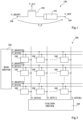
- FIG. 1 schematically illustrates a resistive memory cell 100 according to an example embodiment in which the memory cell 100 is a 1T1R (one transistor, one resistor) cell.
- the cell 100 comprises a variable resistance element 102, which is for example an element based on a metal-insulator-metal (MIM) structure, such as an OxRAM element, where the insulator is for example an oxide, for example comprising HfO 2 , Ta 2 O 5 , or SiO 2 .
- MIM metal-insulator-metal
- the element 102 has two terminals, one being connected to an input/output node 104 of the cell 100 receiving a voltage V_SET, and the other being coupled via the main conducting nodes of a transistor 106 to an input/output node 108 of the cell 100 receiving a voltage V_RESET.
- a control node of the transistor 106 for example receives a control voltage V_ICC.
- a programming voltage V_P is applied between the input/output nodes 104, 108, and the control voltage V_ICC is applied to the control node of the transistor 106 in order to generate a current through the element 102.
- V_ICC the control voltage
- its resistive state is programmed by the level of this current and/or of the voltage V_P.
- the cell 100 is reset when the voltage V_RESET is higher than the voltage V_SET, and is set when the voltage V_SET is higher than the voltage V_RESET.
- the control voltage V_ICC is for example always positive with respect to the voltages V_SET and V_RESET, in other words it is higher than the lowest of the voltages V_SET and V _RESET.
- FIG. 2 schematically illustrates a resistive memory 200 according to an example embodiment.
- the memory 200 for example comprises an array of the memory cells 100 of Figure 1 arranged in rows and columns.
- a row driver (ROW DRIVER) 202 for example supplies the voltages V_RESET and V_ICC to the cells 100 of the array, and for example supplies these voltages on common row lines V _RESET[0] to V _RESET[J] and V_ICC[0] to V_ICC[J], respectively shared by the cells of the rows 0 to J of the array.
- the number J of rows is for example equal to at least two.
- a column driver (COLUMN DRIVER) 204 for example supplies the voltage V_SET to the cells 100 of the array, and for example supplies this voltage on common column lines V_SET[0] to V_SET[K] respectively shared by the columns 0 to K of the array.
- the number K of columns is for example equal to at least two.
- the row and column drivers 202, 204 together form a programming circuit of the memory array capable of programming the resistive state of each memory cell 100.
- resistive memory 200 could be implemented as a cross-bar array in which the transistor 106 of each memory cell is replaced by a two terminal selector element. In such a case, each cell has only two terminals, and it is the row driver 202 that for example applies the programming voltage/current during write operation.
- each memory cell comprises a variable resistance element that is programmed based on a polarity of the voltage/current applied to its terminals
- the variable resistance elements could be unipolar elements that use the same voltage polarity for set and reset programming operations.
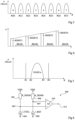
- Figure 3 is a graph representing programmable resistive states of a resistive element according to an example embodiment.
- the x-axis of the graph represents the resistance R using a log scale and the y-axis represents the number of cells (# CELLS).
- the example of Figure 3 corresponds to 3-bit memory cells in which the variable resistance element of each cell is programmable to have one of 8 resistive states labelled 0 to 7 in the example of Figure 3 .
- the resistances of the variable resistance elements programmed within each resistive state n are distributed around a mean level R(n), for example according to a normal distribution. Thus, the resistances associated with each resistive state fall within a corresponding resistance range.
- redundancy in the programmed data may allow the resistance ranges to have little or no gap between them.
- the resistance R(0) has an order of magnitude of 100 to 10,000 ohms
- the resistance R(7) has an order of magnitude of 10 7 to 10 9 ohms.
- Figure 4 is a graph representing an incremental step pulse programming (ISPP) method similar to methods used for programming a flash memory, and that could be applied for programming cells of a resistive memory according to an example embodiment.
- ISPP incremental step pulse programming
- a reset voltage pulse RESET1 is applied to a memory cell.
- this pulse is applied as the signal V_ICC at the control node of the transistor 106 of the cell 100 of Figure 1 , while voltage V_RESET is at a higher level than the voltage V_SET.
- a read operation is performed to detect whether the resistance of the cell has increased sufficiently for it to have passed the lower limit of the resistive state 1. If so, the programming of this cell is complete. If not, a further pulse RESET2 of higher amplitude than the pulse RESET1 is applied to the cell, and a further read operation is performed, and it is again verified whether the lower limit of the state 1 has been exceeded. If so, the programming of this cell is complete. If not, these operations are repeated again and again until it is determined that the lower limit of the target state has been exceeded.
- the increments in the amplitude of the reset pulses are for example chosen such that the corresponding change in resistance will be lower than the resistance range of the targeted state, and as such, there is low risk of overshooting the targeted state. However, this leads to a relatively slow process for bringing a cell to the desired target state.
- Figure 5 is a graph representing resistance thresholds associated with a resistive state according to an example embodiment of the present disclosure. Like in the example of Figure 3 , the x-axis (resistance R) of the graph of Figure 5 uses a log scale.
- a curve in Figure 5 represents the distribution of cells in a resistive memory having a state n, where n is for example from 0 to 7 in the case of 3-bit memory cells, or more generally from 0 to M-1, where there are M states, and M is an integer equal to 2 or more.
- each state n four resistance thresholds R1, R2, R3 and R4 are for example defined. However, in some embodiments, only the thresholds R3 and R4 are defined for the lowest resistive state 0, and only the thresholds R1 and R2 are defined for the highest resistive state M-1.
- the thresholds R2 and R3 are for example respectively low and high resistance thresholds defining lower and upper limits of the resistance distributions in the state n.
- the low threshold R2 corresponds to the low end of the resistance range of the state n
- the high threshold R3 corresponds to the high end of the resistance range of the state n.
- the threshold R2 is at least 10 percent greater than the threshold R1
- the threshold R4 is at least 10 percent greater than the threshold R3.
- the threshold R2 is at least twice the threshold R1
- the threshold R4 is at least twice the threshold R3.
- the threshold R2 is at least ten times the threshold R1
- the threshold R4 is at least ten times the threshold R3.
- the programmed resistance is compared with one or both of the thresholds R2 and R3, and with one or both of the thresholds R1 and R4.
- An example of a comparator for performing such a comparison between a programmed resistance and a resistance threshold will now be described with reference to Figure 6 .
- Figure 6 schematically illustrates a resistance comparator 600 according to an example embodiment.
- An input branch for example comprises a resistor 602 of resistance R_SENSE coupled between a supply rail VDD and an intermediate node 603.
- the node 603 is in turn coupled to the cell having the resistance to be compared.
- This cell is represented by a current source 604 in Figure 6 conducting a current I_CELL during a read operation of the cell to be compared.
- a reference branch for example comprises a resistor 606 having the same resistance R_SENSE as the resistor 602 and coupled between the supply rail VDD and an intermediate node 607.
- the node 607 is in turn coupled to a reference cell having the threshold resistance.
- This reference cell is represented by a current source 608 in Figure 6 conducting a current I_REF.
- the resistance of this reference cell corresponds to one of the threshold resistances R1, R2, R3 and R4 of a given state n.
- the intermediate nodes 603 and 607 are for example respectively coupled to positive and negative inputs of a sense amplifier (SA) 610, which provides at its output 612 a signal indicating when the current I_CELL is lower than the current I_REF, indicating that the resistance of the cell to be compared is higher than the threshold resistance.
- SA sense amplifier
- a comparator similar to the one of Figure 6 is provided for each of the resistance thresholds R1 to R4 for each of the states n. In some embodiments there may however be some common thresholds among the various states. These comparators for example form part of the programming circuit of the resistive memory. For example, they could be implemented in the row driver 202 of Figure 2 .
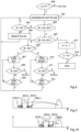
- Figure 7 is a flow diagram representing operations in a method of programming one or more cells of a resistive memory array according to an example embodiment. This method is for example implemented by a programming circuit of a resistive memory, such as by the row and column drivers 202, 204 of Figure 2 and by resistance comparators like the comparator 600 of Figure 6 .
- the cells of the resistive memory are for example brought to an initial state, which is for example the highest or lowest resistive state.
- this is performed by a SET or RESET operation of all the cells, the operation that is most energy consuming being used. Indeed, this can allow the subsequent operations, which take more time, to use less energy. Alternatively, the operation that is the most time consuming could be used, as this can allow subsequent operations, which are more numerous, to be performed more quickly.
- an operation is applied to bring all of the cells to the highest resistive state. For example, a reset operation is used to bring all of the cells to the state 7 of Figure 3 .
- a variable n representing the state is set to a first target state to be programmed.
- the first target state is the state 0.
- the initial state of the memory cells is the highest resistive state (the state 7 in the example of Figure 3 )
- the first state to be programmed is the state 0
- the first state to be programmed is the highest resistive state (the state 7 in the example of Figure 3 ).
- the programming circuit includes a lookup table indicating, for each state n, the voltage level of the voltage V_ICC that should be applied to a cell in order to reach a target resistance range associated with the state n.
- a SET pulse is applied in order to reduce the resistance of one or more cells to the target resistive state n, which is initially the state 0.
- the programmed resistance R of each of the programmed cells is for example compared with the resistance thresholds R1 and R4 of the state n, or only the threshold R4 in the case of the state 0, or only the threshold R1 in the case of the highest resistive state (the state 7 in the example of Figure 3 ). If the resistance R of any cell is lower than R1 or higher than R4, then that cell has not reached the target range associated with the state n. In such a case, a new attempt is for example made to bring that cell to the target range of state n. For example, this involves applying a reset pulse in an operation 706 to reset the cell to state 7, and then repeating operations 704 and 705.
- a limit is set on the number of times the loop formed of operations 704, 705 and 706 is executed for a given cell. For example, once a certain limit, such as one hundred attempts, has been reached, the cell is deemed faulty, and no longer used.
- the fine resistance control sequence involves applying a voltage V_ICC pulse at the level determined in operation 703 for the state n, while the voltage V_P is adjusted in order to increase or decrease the programmed resistance of the concerned cells.
- the fine resistance control method for example involves an operation 708 in which it is determined whether the resistance of the cell is above or below the resistance range of the state n. This is for example determined by comparing the resistance R of the cell with the resistance threshold R3, although it could equally be performed by comparing the resistance R of the cell with the resistance threshold R2.
- an operation 710 it is determined whether the resistance R is now less than or equal to the resistance threshold R3. If not, in an operation 711, it is determined whether the end of the fine resistance control sequence has been reached, in other words whether all available voltage levels have been applied. If not, the operations 709, 710 and 711 are repeated with the next voltage increment to reduce the resistance by the relatively fine variation, until the resistance R is equal to or less than the threshold R3, or the end of the fine resistance control sequence is reached. If, in operation 710, the resistance R is found to be equal to or less than R3, the next operation is an operation 715. Alternatively, if in operation 711 the end of the sequence is reached, the method for example returns to the operation 706.
- a fine reset operation is performed in an operation 712. This for example involves increasing the resistance by a relatively fine variation.
- this relatively fine variation is equal to or less than (R2-R1)/2, and in some cases equal to or less than (R2-R1)/10, where R1 and R2 are for example the values for the current state n, or the median values among all the states.
- the relatively fine variable is an amount less than the resistance range of the state n, i.e. R3-R2.
- an operation 713 it is determined whether the resistance R is now greater than or equal to the resistance threshold R2. If not, in an operation 714, it is determined whether the end of the fine resistance control sequence has been reached, in other words whether all available voltage levels have been applied. If not, the operations 712, 713 and 714 are repeated with the next voltage increment to increase the resistance by the relatively fine variation, until the resistance R is equal to or greater than the threshold R2, or the end of the fine resistance control sequence is reached. If, in operation 713, the resistance R is found to be equal to or greater than R3, the next operation is an operation 715. Alternatively, if in operation 714 the end of the sequence is reached, the method for example returns to the operation 706.
- n is equal to its final level N. If not, the method for example returns to operation 703 based on the new state n. If all of the states have been programmed, the method for example ends.
- an incremental compliance current method could instead be applied, in which, similar to the ISPP method, the voltage V_ICC is increased in increments until the target range between the thresholds R1 to R4 is reached.
- a combination of the state dependent retry method and the incremental compliance current method can be used, as will now be described with reference to Figure 8 .
- Figure 8 is a flow diagram representing operations in a method of programming one or more cells of a resistive memory according to a further example embodiment. The method of Figure 8 is for example performed instead of the operation 716 of Figure 7 .
- variable n is compared to a variable N', which is for example an intermediate state between the further state and the initial state. Assuming that the initial state is state 7 and programming starts with state 0, the state N' is for example the state 3, 4 or 5. Until the variable n reaches N', the method for example returns from operation 800 to operation 703 of Figure 7 . Once n is equal to N', an operation 801 of Figure 8 is performed.
- the set pulse is moderated, for example based on the ISPP method.
- this for example involves applying an initial pulse using a first voltage level of the signal V_ICC to the cells to be programmed.
- the programmed resistance R of each of the programmed cells is for example compared with the resistance thresholds R1 and R4 of the state n, or only the threshold R1 in the case of the highest resistive state (the state 7 in the example of Figure 3 ). If the resistance R of any cell is lower than R1 or higher than R4, then that cell has not reached the target range associated with the state n. In such a case, a new attempt is for example made to bring that cell to the target range of state n. This now involves repeating the operation 801 based on the next current increment, achieved for example by incrementing the voltage level of V_ICC.
- an operation 803 is implemented in which the programmed resistance R is compared to R1, and if R is not greater than R1, prior to repeating operation 801, a reset pulse is applied in an operation 804. This for example avoids a situation in which the target resistance range of the target state is exceeded, and the operation 801 modifies the resistance in the wrong direction. Operations 801 and 802 are then repeated until the resistance falls within the target range defined by the threshold R1 and/or R4 of the state n. Once this range has been reached, operations 805 to 814 are performed for each cell, these operations being respectively the same as operations 707 to 716 of Figure 7 , and will not be described again.
- Figure 9 is a graph representing the programming of a first memory cell according to the method of Figure 7 , for n less than N'.
- the cells to be programmed with the state 1 are brought from the state 7 to the target range of the state 1 defined by the thresholds R1(1) and R4(1) of the state 1.
- the state dependent retry method is applied for cells having resistances falling outside the range R1(1) to R4(1).
- the fine resistance control method is applied to bring the resistances within the range of the target state.
- Figure 10 is a graph representing the programming of a second memory cell according to the method of Figure 8 for n equal to or greater than N'.
- the cells to be programmed with the state 6 are brought from the state 7 to the target range of the state 6 defined by the thresholds R1(6) and R4(6) of the state 6.
- the incremental compliance current method is applied for cells having resistances falling outside the range R1(6) to R4(6).
- the fine resistance control method is applied to bring the resistances within the range of the target state.
- the methods described herein for programming the resistive states of cells of a resistive memory can be applied to any resistance ranges of the resistive states, with or without gaps between the ranges.
- the resistance ranges are defined based on the techniques described in the publication entitled " Resistive RAM with multiple bits per cell: array-level demonstration of 3 bits per cell", Binh Le, A. Grossi, E. Vianello, T. Wu, G. Lama, E. Beigné, H-.S. Philip Wong, and Sabhasish Mitra, IEEE TED vol 66 no 1 January 2019 .
- An example of the application of this technique will now be described with reference to Figure 11 .
- Figure 11 is a graph representing a distribution of resistance ranges and gaps between ranges for a 3-bit cell according to an example embodiment.
- the widths of distributions are multiples of standard variations. In other embodiments the widths of distributions are multiples of two or more standard variations. For example, for distribution 1, we can use 3 sigmas, but for distribution 7, we can use 2.5 sigmas.
- a method in a multi-bit per cell RRAM for dividing the available resistance window into ranges for multiple resistance distributions to improve read and program performance comprises assigning non-uniform resistance ranges to multi-bit per cell RRAM distributions based on the intrinsic variation of RRAM memory cells; and assigning non-uniform gaps between the distributions based on sense-amplifier sensing margin requirement.
- An advantage of the embodiments described herein is that the resistive states of cells of a resistive memory can be programmed in a relative fast and energy efficient manner.
- variable resistance elements that are set and reset as a function of the polarity of the voltage applied across their terminals
Landscapes
- Engineering & Computer Science (AREA)
- Chemical & Material Sciences (AREA)
- Materials Engineering (AREA)
- Computer Hardware Design (AREA)
- Semiconductor Memories (AREA)
Claims (14)
- Ein Verfahren zum Programmieren von Widerstandsspeicherzellen eines Widerstandsspeichers, wobei das Verfahren Folgendes aufweist:
a) Anwenden, durch eine Programmierschaltung basierend auf einem ersten Zielwiderstandszustand (n), einer anfänglichen Widerstandsmodifikation an eine erste Zelle des Widerstandsspeichers zum Ändern des Widerstands der ersten Zelle von einem anfänglichen Widerstandszustand zu einem ersten neuen Widerstand (R), wobei der erste Zielwiderstandszustand (n) einer von M Widerstandszuständen ist, wobei M eine ganze Zahl gleich 2 oder größer ist; und entweder:b1) Vergleichen, durch die Programmierschaltung, des ersten neuen Widerstands (R) der ersten Zelle mit einem Widerstandsbereich ([R2(n); R3(n)]) des ersten Ziel-Widerstandszustands (n), wobei der Widerstandsbereich durch einen zweiten Widerstandsschwellenwert (R2(n)) und einen dritten Widerstandsschwellenwert (R3(n)) definiert ist, wobei der dritte Widerstandsschwellenwert höher ist als der zweite Widerstandsschwellenwert;c1) Vergleichen, durch die Programmierschaltung, des ersten neuen Widerstands (R) der ersten Zelle mit einem Ziel-Widerstandsbereich ([R1(n); R4(n)]), der mit dem ersten Ziel-Widerstandszustand (n) assoziiert ist, wobei der Ziel-Widerstandsbereich durch einen ersten Widerstandsschwellenwert (R1(n)) und einen vierten Widerstandsschwellenwert (R4(n)) definiert ist, wobei der erste Widerstandsschwellenwert niedriger als der zweite Widerstandsschwellenwert ist und der vierte Widerstandsschwellenwert höher als der dritte Widerstandsschwellenwert ist; undd1) wenn bestimmt wird, dass der erste neue Widerstand (R) außerhalb des Widerstandsbereichs des ersten Zielwiderstandszustands (n) und innerhalb des Zielwiderstandsbereichs liegt, Anwenden, durch die Programmierschaltung, einer oder mehrerer weiterer Widerstandsmodifikationen auf die erste Zelle zum Erhöhen oder Verringern ihres Widerstands; oder im Fall, dass der erste Ziel-Widerstandszustand der niedrigste Widerstandszustand 0 ist:b2) Vergleichen, durch die Programmierschaltung, des ersten neuen Widerstands (R) der ersten Zelle mit dem dritten Widerstandsschwellenwert (R3(n));c2) Vergleichen, durch die Programmierschaltung, des ersten neuen Widerstands (R) der ersten Zelle mit dem vierten Widerstandsschwellenwert (R4(n)); undd2) wenn bestimmt wird, dass der erste neue Widerstand (R) zwischen dem dritten und dem vierten Widerstandsschwellenwert liegt, Anwenden, durch die Programmierschaltung, einer oder mehrerer weiterer Widerstandsmodifikationen auf die erste Zelle zum Verringern ihres Widerstands; oder im Fall, dass der erste Zielwiderstandszustand der höchste Widerstandszustand M-1 ist:b3) Vergleichen, durch die Programmierschaltung, des ersten neuen Widerstands (R) der ersten Zelle mit dem zweiten Widerstandsschwellenwert (R2(n));c3) Vergleichen, durch die Programmierschaltung, des ersten neuen Widerstands (R) der ersten Zelle mit dem ersten Widerstandsschwellenwert (R1(n)); undd3) wenn bestimmt wird, dass der erste neue Widerstand (R) zwischen dem ersten und dem zweiten Widerstandsschwellenwert liegt, Anwenden, durch die Programmierschaltung, einer oder mehrerer weiterer Widerstandsmodifikationen auf die erste Zelle zum Erhöhen ihres Widerstands. - Das Verfahren nach Anspruch 1, das ferner Folgendes aufweist:- wenn in den Schritten b1) und c1) bestimmt wird, dass der erste neue Widerstand (R) unterhalb des Widerstandsbereichs des Ziel-Widerstandszustands liegt, Anwenden, durch die Programmierschaltung in Schritt d1), wenigstens einer weiteren Widerstandsmodifikation auf die erste Zelle zum Erhöhen ihres Widerstands; und- wenn in den Schritten b1) und c1) bestimmt wird, dass der erste neue Widerstand (R) oberhalb des Widerstandsbereichs des Ziel-Widerstandszustands liegt, Anwenden, durch die Programmierschaltung, wenigstens einer weiteren Widerstandsmodifikation auf die erste Zelle zum Verringern ihres Widerstands.
- Das Verfahren nach Anspruch 1 oder 2, wobei jede der einen oder mehreren weiteren Widerstandsmodifikationen den Widerstand der ersten Zelle modifiziert um weniger als:- die Hälfte der Differenz zwischen dem ersten Widerstandsschwellenwert (R1(n)) und dem zweiten Widerstandsschwellenwert (R2(n)); oder- die Hälfte der Differenz zwischen dem dritten Widerstandsschwellenwert (R3(n)) und dem vierten Widerstandsschwellenwert (R4(n)).
- Das Verfahren nach einem der Ansprüche 1 bis 3, wobei die anfängliche Widerstandsmodifikation den Widerstand der ersten Zelle modifiziert um mehr als:- die Hälfte der Differenz zwischen dem ersten Widerstandsschwellenwert (R1(n)) und dem zweiten Widerstandsschwellenwert (R2(n)); oder- die Hälfte der Differenz zwischen dem dritten Widerstandsschwellenwert (R3(n)) und dem vierten Widerstandsschwellenwert (R4(n)).
- Das Verfahren nach einem der Ansprüche 1 bis 4, wobei, wenn in den Schritten b1) und c1) bestimmt wird, dass der erste neue Widerstand (R) innerhalb des Widerstandsbereichs des Ziel-Widerstandszustands (n) liegt, keine weitere Widerstandsmodifikation auf die erste Zelle angewendet wird.
- Das Verfahren nach einem der Ansprüche 1 bis 5, wobei die erste Zelle ein erstes variables Widerstandselement (102) aufweist, das mit einem ersten Transistor (106) in Reihe geschaltet ist, und wobei Anwenden, durch die Programmierschaltung, der anfänglichen Widerstandsmodifikation auf die erste Zelle Folgendes aufweist:- Anlegen einer ersten Programmierspannung (V_P) über dem ersten variablen Widerstandselement (102); und- Anlegen einer Steuerspannung (V_ICC) mit einem ersten Pegel an den ersten Transistor (106), wobei der erste Pegel basierend auf dem ersten Ziel-Widerstandszustand (n) ausgewählt wird.
- Das Verfahren nach Anspruch 6, aufweisend Anwenden, durch die Programmierschaltung, in Schritt d1), d2) oder d3) von wenigstens einer weiteren Widerstandsmodifikation auf die erste Zelle durch Anlegen einer zweiten Programmierspannung (V_P) über dem ersten variablen Widerstandselement, wobei die zweite Programmierspannung auf einem anderen Pegel als die erste Programmierspannung ist.
- Das Verfahren nach einem der Ansprüche 1 bis 7, wobei der zweite Widerstandsschwellenwert (R2) mindestens 10 Prozent höher ist als der erste Widerstandsschwellenwert (R1(n)) und der vierte Widerstandsschwellenwert (R4(n)) mindestens 10 Prozent höher ist als der dritte Widerstandsschwellenwert (R3).
- Das Verfahren nach einem der Ansprüche 1 bis 8, das ferner Folgendes aufweist:
e) Anwenden, durch die Programmierschaltung, basierend auf einem zweiten Ziel-Widerstandszustand (n), einer anfänglichen Widerstandsmodifikation auf eine zweite Zelle des Widerstandsspeichers zum Ändern ihres Widerstands von dem anfänglichen Widerstandszustand auf einen zweiten neuen Widerstand (R); und entweder:f1) Vergleichen, durch die Programmierschaltung, des zweiten neuen Widerstands (R) der zweiten Zelle mit einem zweiten Widerstandsbereich ([R2(n); R3(n)]) des zweiten Ziel-Widerstandszustands (n), wobei der zweite Widerstandsbereich durch einen zweiten Widerstandsschwellenwert (R2(n)) und einen dritten Widerstandsschwellenwert (R3(n)) definiert ist, wobei der dritte Widerstandsschwellenwert höher ist als der zweite Widerstandsschwellenwert;g1) Vergleichen, durch die Programmierschaltung, des zweiten neuen Widerstands (R) der zweiten Zelle mit einem zweiten Ziel-Widerstandsbereich ([R1(n); R4(n)]), der mit dem zweiten Ziel-Widerstandszustand (n) assoziiert ist, wobei der zweite Ziel-Widerstandsbereich durch einen ersten Widerstandsschwellenwert (R1(n)) und einen vierten Widerstandsschwellenwert (R4(n)) definiert ist, wobei der erste Widerstandsschwellenwert niedriger als der zweite Widerstandsschwellenwert ist und der vierte Widerstandsschwellenwert höher als der dritte Widerstandsschwellenwert ist; undh1) wenn bestimmt wird, dass der zweite neue Widerstand (R) außerhalb des Widerstandsbereichs des zweiten Ziel-Widerstandszustands (n) und innerhalb des zweiten Ziel-Widerstandsbereichs liegt, Anwenden, durch die Programmierschaltung, einer oder mehrerer weiterer Widerstandsmodifikationen auf die zweite Zelle zum Erhöhen oder Verringern ihres Widerstands; oder im Fall, dass der zweite Ziel-Widerstandszustand der niedrigste Widerstandszustand 0 ist:b2) Vergleichen, durch die Programmierschaltung, des zweiten neuen Widerstands (R) der zweiten Zelle mit dem dritten Widerstandsschwellenwert (R3(n)) des zweiten Ziel-Widerstandszustands (n);c2) Vergleichen, durch die Programmierschaltung, des zweiten neuen Widerstands (R) der zweiten Zelle mit dem vierten Widerstandsschwellenwert (R4(n)) des zweiten Ziel-Widerstandszustands (n); undd2) wenn bestimmt wird, dass der zweite neue Widerstand (R) zwischen dem dritten und dem vierten Widerstandsschwellenwert des zweiten Ziel-Widerstandszustands (n) liegt, Anwenden, durch die Programmierschaltung, einer oder mehrerer weiterer Widerstandsmodifikationen auf die zweite Zelle zum Verringern ihres Widerstands; oder im Fall, dass der zweite Ziel-Widerstandszustand der höchste Widerstandszustand M-1 ist:b3) Vergleichen, durch die Programmierschaltung, des zweiten neuen Widerstands (R) der zweiten Zelle mit dem zweiten Widerstandsschwellenwert (R2(n)) des zweiten Ziel-Widerstandszustands (n);c3) Vergleichen, durch die Programmierschaltung, des zweiten neuen Widerstands (R) der zweiten Zelle mit dem ersten Widerstandsschwellenwert (R1(n)) des zweiten Ziel-Widerstandszustands (n); undd3) wenn bestimmt wird, dass der zweite neue Widerstand (R) zwischen dem ersten und dem zweiten Widerstandsschwellenwert des zweiten Ziel-Widerstandszustands (n) liegt, Anwenden, durch die Programmierschaltung, einer oder mehrerer weiterer Widerstandsmodifikationen auf die zweite Zelle zum Erhöhen ihres Widerstands. - Das Verfahren nach Anspruch 9 in Abhängigkeit von Anspruch 6 oder 7, wobei die zweite Zelle ein zweites variables Widerstandselement (102) aufweist, das mit einem zweiten Transistor (106) in Reihe geschaltet ist, und wobei Anlegen, durch die Programmierschaltung, der anfänglichen Widerstandsmodifikation an die zweite Zelle Anlegen einer Steuerspannung (V_ICC) mit einem zweiten Pegel an den zweiten Transistor (106) aufweist, wobei der zweite Pegel sich von dem ersten Pegel unterscheidet und basierend auf dem zweiten Ziel-Widerstandszustand (n) ausgewählt wird.
- Das Verfahren nach Anspruch 9 oder 10, das ferner Folgendes aufweist:- Bestimmen in den Schritten b1) und c1), dass der erste neue Widerstand (R) der ersten Zelle außerhalb des ersten Ziel-Widerstandsbereichs liegt, und Wiederholen der anfänglichen Widerstandsmodifikation; und- Bestimmen in den Schritten f1) und g1), dass der zweite neue Widerstand (R) der zweiten Zelle außerhalb des zweiten Ziel-Widerstandsbereichs liegt, und Anwenden einer weiteren anfänglichen Widerstandsmodifikation.
- Eine Programmierschaltung zum Programmieren von Widerstandsspeicherzellen eines Widerstandsspeichers, wobei die Programmierschaltung konfiguriert ist zum:
a) Anwenden, basierend auf einem ersten Ziel-Widerstandszustand (n), einer anfänglichen Widerstandsmodifikation auf eine erste Zelle des Widerstandsspeichers zum Ändern des Widerstands der ersten Zelle von einem anfänglichen Widerstandszustand zu einem ersten neuen Widerstand (R), wobei der erste Ziel-Widerstandszustand (n) einer von M Widerstandszuständen ist, wobei M eine ganze Zahl gleich 2 oder größer ist; und entweder:b1) Vergleichen des ersten neuen Widerstands (R) der ersten Zelle mit einem Widerstandsbereich ([R2(n); R3(n)]) des ersten Ziel-Widerstandszustands (n), wobei der Widerstandsbereich durch einen zweiten Widerstandsschwellenwert (R2(n)) und einen dritten Widerstandsschwellenwert (R3(n)) definiert ist, wobei der dritte Widerstandsschwellenwert höher ist als der zweite Widerstandsschwellenwert;c1) Vergleichen des ersten neuen Widerstands (R) der ersten Zelle mit einem Ziel-Widerstandsbereich ([R1(n); R4(n)]) des ersten Ziel-Widerstandszustands (n), wobei der Ziel-Widerstandsbereich durch einen ersten Widerstandsschwellenwert (R1(n)) und einen vierten Widerstandsschwellenwert (R4(n)) definiert ist, wobei der erste Widerstandsschwellenwert niedriger als der zweite Widerstandsschwellenwert ist und der vierte Widerstandsschwellenwert höher als der dritte Widerstandsschwellenwert ist; undd1) wenn bestimmt wird, dass der erste neue Widerstand (R) außerhalb des Widerstandsbereichs des ersten Ziel-Widerstandszustands (n) und innerhalb des Ziel-Widerstandsbereichs liegt, Anwenden einer oder mehrerer weiterer Widerstandsmodifikationen auf die erste Zelle zum Erhöhen oder Verringern ihres Widerstands; oder im Fall, dass der erste Ziel-Widerstandszustand der niedrigste Widerstandszustand 0 ist:b2) Vergleichen des ersten neuen Widerstands (R) der ersten Zelle mit dem dritten Widerstandsschwellenwert (R3(n));c2) Vergleichen des ersten neuen Widerstands (R) der ersten Zelle mit dem vierten Widerstandsschwellenwert (R4(n)); undd2) wenn bestimmt wird, dass der erste neue Widerstand (R) zwischen dem dritten und dem vierten Widerstandsschwellenwert liegt, Anwenden einer oder mehrerer weiterer Widerstandsmodifikationen auf die erste Zelle zum Verringern ihres Widerstands; oder im Fall, dass der erste Ziel-Widerstandszustand der höchste Widerstandszustand M-1 ist:b3) Vergleichen des ersten neuen Widerstands (R) der ersten Zelle mit dem zweiten Widerstandsschwellenwert (R2(n));c3) Vergleichen des ersten neuen Widerstands (R) der ersten Zelle mit dem ersten Widerstandsschwellenwert (R1(n)); undd3) wenn bestimmt wird, dass der erste neue Widerstand (R) zwischen dem ersten und dem zweiten Widerstandsschwellenwert liegt, Anwenden einer oder mehrerer weiterer Widerstandsmodifikationen auf die erste Zelle zum Erhöhen ihres Widerstands. - Ein Widerstandsspeicher, der Folgendes aufweist:- ein Array von Zellen; und- die Programmierschaltung nach Anspruch 12, konfiguriert zum Programmieren der Zellen des Arrays.
- Der Widerstandsspeicher nach Anspruch 13, wobei die Zellen des Arrays jeweils programmierbar sind zum Speichern einer Vielzahl von Bits durch Programmieren eines von drei oder mehr Widerstandszuständen.
Applications Claiming Priority (2)
| Application Number | Priority Date | Filing Date | Title |
|---|---|---|---|
| US201862653398P | 2018-04-05 | 2018-04-05 | |
| PCT/IB2019/000432 WO2019193423A1 (en) | 2018-04-05 | 2019-04-05 | Circuit and method for programming resistive memory cells |
Publications (2)
| Publication Number | Publication Date |
|---|---|
| EP3776554A1 EP3776554A1 (de) | 2021-02-17 |
| EP3776554B1 true EP3776554B1 (de) | 2025-06-04 |
Family
ID=66867574
Family Applications (1)
| Application Number | Title | Priority Date | Filing Date |
|---|---|---|---|
| EP19730912.3A Active EP3776554B1 (de) | 2018-04-05 | 2019-04-05 | Schaltung und verfahren zur programmierung resistiver speicherzellen |
Country Status (3)
| Country | Link |
|---|---|
| US (1) | US11217307B2 (de) |
| EP (1) | EP3776554B1 (de) |
| WO (1) | WO2019193423A1 (de) |
Families Citing this family (2)
| Publication number | Priority date | Publication date | Assignee | Title |
|---|---|---|---|---|
| FR3148862B1 (fr) * | 2023-05-19 | 2025-10-17 | St Microelectronics Int Nv | Lecture d’un dispositif de mémoire non volatile multi-niveaux, en particulier à changement de phase, et dispositif de mémoire non volatile multi-niveaux |
| CN119851719B (zh) * | 2024-12-24 | 2026-04-28 | 北方集成电路技术创新中心(北京)有限公司 | 一种用于提高器件保持特性的忆阻器多值编程方法 |
Family Cites Families (6)
| Publication number | Priority date | Publication date | Assignee | Title |
|---|---|---|---|---|
| JP4205938B2 (ja) * | 2002-12-05 | 2009-01-07 | シャープ株式会社 | 不揮発性メモリ装置 |
| US7940552B2 (en) * | 2007-04-30 | 2011-05-10 | Samsung Electronics Co., Ltd. | Multiple level cell phase-change memory device having pre-reading operation resistance drift recovery, memory systems employing such devices and methods of reading memory devices |
| JP2009099206A (ja) | 2007-10-17 | 2009-05-07 | Toshiba Corp | 抵抗変化メモリ装置 |
| KR20130015930A (ko) | 2011-08-05 | 2013-02-14 | 에스케이하이닉스 주식회사 | 비휘발성 메모리 시스템 및 이를 위한 프로그램 방법 |
| US8908426B2 (en) * | 2012-12-04 | 2014-12-09 | Macronix International Co., Ltd. | Cell sensing circuit for phase change memory and methods thereof |
| US9613693B1 (en) | 2015-10-29 | 2017-04-04 | Adesto Technologies Corporation | Methods for setting a resistance of programmable resistance memory cells and devices including the same |
-
2019
- 2019-04-05 US US15/733,715 patent/US11217307B2/en not_active Expired - Fee Related
- 2019-04-05 WO PCT/IB2019/000432 patent/WO2019193423A1/en not_active Ceased
- 2019-04-05 EP EP19730912.3A patent/EP3776554B1/de active Active
Also Published As
| Publication number | Publication date |
|---|---|
| EP3776554A1 (de) | 2021-02-17 |
| WO2019193423A1 (en) | 2019-10-10 |
| US11217307B2 (en) | 2022-01-04 |
| US20210035638A1 (en) | 2021-02-04 |
Similar Documents
| Publication | Publication Date | Title |
|---|---|---|
| KR101310991B1 (ko) | 상변화 메모리를 위한 판독 분포 관리 | |
| JP5478861B2 (ja) | 相変化物質をプログラミングする方法 | |
| US7907437B2 (en) | Resistance variable memory device and method of writing data | |
| US8848430B2 (en) | Step soft program for reversible resistivity-switching elements | |
| US8861258B2 (en) | Set/reset algorithm which detects and repairs weak cells in resistive-switching memory device | |
| EP3201925B1 (de) | Vorrichtung und verfahren zur erfassung von hard-bits und soft-bits | |
| US8625326B2 (en) | Non-volatile semiconductor memory device with a resistance adjusting circuit and an operation method thereof | |
| US9887009B2 (en) | Memory page buffer with simultaneous multiple bit programming capability | |
| Ramadan et al. | Adaptive programming in multi-level cell ReRAM | |
| KR20100068462A (ko) | 저항 변화 메모리 장치 | |
| US11929124B2 (en) | Method and system for accessing memory cells | |
| JP2015506529A (ja) | 相変化メモリをプログラミングするための方法、駆動回路 | |
| EP3553781A1 (de) | Erfassung eines speichers mit veränderlichem widerstand | |
| WO2022013589A1 (en) | Methods and systems for improving access to memory cells | |
| US11217307B2 (en) | Circuit and method for programming resistive memory cells | |
| US10559354B2 (en) | Memory system | |
| CN114746945A (zh) | 用于稳定单元阈值电压的系统及方法 | |
| TWI760924B (zh) | 用於存取記憶體單元之方法及系統 | |
| US20250022509A1 (en) | Method of operating phase change memories, corresponding device and computer program product | |
| US20140160872A1 (en) | Voltage generation circuit, and write driver and semiconductor memory apparatus including the same | |
| JP6906660B1 (ja) | 抵抗変化型メモリ保存装置およびその操作方法 | |
| JP6972059B2 (ja) | 抵抗変化型メモリ | |
| CN121075390A (zh) | 用于rerams的智能分组和修复编程的系统和方法 | |
| US20220199181A1 (en) | Memory device having reference memory array structure resembling data memory array structure, and methods of operating the same |
Legal Events
| Date | Code | Title | Description |
|---|---|---|---|
| STAA | Information on the status of an ep patent application or granted ep patent |
Free format text: STATUS: UNKNOWN |
|
| STAA | Information on the status of an ep patent application or granted ep patent |
Free format text: STATUS: THE INTERNATIONAL PUBLICATION HAS BEEN MADE |
|
| PUAI | Public reference made under article 153(3) epc to a published international application that has entered the european phase |
Free format text: ORIGINAL CODE: 0009012 |
|
| STAA | Information on the status of an ep patent application or granted ep patent |
Free format text: STATUS: REQUEST FOR EXAMINATION WAS MADE |
|
| 17P | Request for examination filed |
Effective date: 20201006 |
|
| AK | Designated contracting states |
Kind code of ref document: A1 Designated state(s): AL AT BE BG CH CY CZ DE DK EE ES FI FR GB GR HR HU IE IS IT LI LT LU LV MC MK MT NL NO PL PT RO RS SE SI SK SM TR |
|
| AX | Request for extension of the european patent |
Extension state: BA ME |
|
| DAV | Request for validation of the european patent (deleted) | ||
| DAX | Request for extension of the european patent (deleted) | ||
| STAA | Information on the status of an ep patent application or granted ep patent |
Free format text: STATUS: EXAMINATION IS IN PROGRESS |
|
| 17Q | First examination report despatched |
Effective date: 20211109 |
|
| GRAP | Despatch of communication of intention to grant a patent |
Free format text: ORIGINAL CODE: EPIDOSNIGR1 |
|
| STAA | Information on the status of an ep patent application or granted ep patent |
Free format text: STATUS: GRANT OF PATENT IS INTENDED |
|
| INTG | Intention to grant announced |
Effective date: 20240122 |
|
| GRAJ | Information related to disapproval of communication of intention to grant by the applicant or resumption of examination proceedings by the epo deleted |
Free format text: ORIGINAL CODE: EPIDOSDIGR1 |
|
| STAA | Information on the status of an ep patent application or granted ep patent |
Free format text: STATUS: EXAMINATION IS IN PROGRESS |
|
| INTC | Intention to grant announced (deleted) | ||
| RAP3 | Party data changed (applicant data changed or rights of an application transferred) |
Owner name: THE BOARD OF TRUSTEES OF THE LELAND STANFORDJUNIOR UNIVERSITY Owner name: COMMISSARIAT A L'ENERGIE ATOMIQUE ET AUX ENERGIESALTERNATIVES |
|
| GRAP | Despatch of communication of intention to grant a patent |
Free format text: ORIGINAL CODE: EPIDOSNIGR1 |
|
| STAA | Information on the status of an ep patent application or granted ep patent |
Free format text: STATUS: GRANT OF PATENT IS INTENDED |
|
| INTG | Intention to grant announced |
Effective date: 20250116 |
|
| GRAS | Grant fee paid |
Free format text: ORIGINAL CODE: EPIDOSNIGR3 |
|
| GRAA | (expected) grant |
Free format text: ORIGINAL CODE: 0009210 |
|
| STAA | Information on the status of an ep patent application or granted ep patent |
Free format text: STATUS: THE PATENT HAS BEEN GRANTED |
|
| AK | Designated contracting states |
Kind code of ref document: B1 Designated state(s): AL AT BE BG CH CY CZ DE DK EE ES FI FR GB GR HR HU IE IS IT LI LT LU LV MC MK MT NL NO PL PT RO RS SE SI SK SM TR |
|
| REG | Reference to a national code |
Ref country code: GB Ref legal event code: FG4D |
|
| REG | Reference to a national code |
Ref country code: CH Ref legal event code: EP |
|
| REG | Reference to a national code |
Ref country code: DE Ref legal event code: R096 Ref document number: 602019070744 Country of ref document: DE |
|
| REG | Reference to a national code |
Ref country code: IE Ref legal event code: FG4D |
|
| REG | Reference to a national code |
Ref country code: NL Ref legal event code: MP Effective date: 20250604 |
|
| PG25 | Lapsed in a contracting state [announced via postgrant information from national office to epo] |
Ref country code: FI Free format text: LAPSE BECAUSE OF FAILURE TO SUBMIT A TRANSLATION OF THE DESCRIPTION OR TO PAY THE FEE WITHIN THE PRESCRIBED TIME-LIMIT Effective date: 20250604 Ref country code: ES Free format text: LAPSE BECAUSE OF FAILURE TO SUBMIT A TRANSLATION OF THE DESCRIPTION OR TO PAY THE FEE WITHIN THE PRESCRIBED TIME-LIMIT Effective date: 20250604 |
|
| REG | Reference to a national code |
Ref country code: LT Ref legal event code: MG9D |
|
| PG25 | Lapsed in a contracting state [announced via postgrant information from national office to epo] |
Ref country code: NO Free format text: LAPSE BECAUSE OF FAILURE TO SUBMIT A TRANSLATION OF THE DESCRIPTION OR TO PAY THE FEE WITHIN THE PRESCRIBED TIME-LIMIT Effective date: 20250904 Ref country code: GR Free format text: LAPSE BECAUSE OF FAILURE TO SUBMIT A TRANSLATION OF THE DESCRIPTION OR TO PAY THE FEE WITHIN THE PRESCRIBED TIME-LIMIT Effective date: 20250905 |
|
| PG25 | Lapsed in a contracting state [announced via postgrant information from national office to epo] |
Ref country code: PL Free format text: LAPSE BECAUSE OF FAILURE TO SUBMIT A TRANSLATION OF THE DESCRIPTION OR TO PAY THE FEE WITHIN THE PRESCRIBED TIME-LIMIT Effective date: 20250604 |
|
| PG25 | Lapsed in a contracting state [announced via postgrant information from national office to epo] |
Ref country code: BG Free format text: LAPSE BECAUSE OF FAILURE TO SUBMIT A TRANSLATION OF THE DESCRIPTION OR TO PAY THE FEE WITHIN THE PRESCRIBED TIME-LIMIT Effective date: 20250604 |
|
| PG25 | Lapsed in a contracting state [announced via postgrant information from national office to epo] |
Ref country code: HR Free format text: LAPSE BECAUSE OF FAILURE TO SUBMIT A TRANSLATION OF THE DESCRIPTION OR TO PAY THE FEE WITHIN THE PRESCRIBED TIME-LIMIT Effective date: 20250604 |
|
| PG25 | Lapsed in a contracting state [announced via postgrant information from national office to epo] |
Ref country code: RS Free format text: LAPSE BECAUSE OF FAILURE TO SUBMIT A TRANSLATION OF THE DESCRIPTION OR TO PAY THE FEE WITHIN THE PRESCRIBED TIME-LIMIT Effective date: 20250904 |
|
| PG25 | Lapsed in a contracting state [announced via postgrant information from national office to epo] |
Ref country code: LV Free format text: LAPSE BECAUSE OF FAILURE TO SUBMIT A TRANSLATION OF THE DESCRIPTION OR TO PAY THE FEE WITHIN THE PRESCRIBED TIME-LIMIT Effective date: 20250604 |
|
| PG25 | Lapsed in a contracting state [announced via postgrant information from national office to epo] |
Ref country code: NL Free format text: LAPSE BECAUSE OF FAILURE TO SUBMIT A TRANSLATION OF THE DESCRIPTION OR TO PAY THE FEE WITHIN THE PRESCRIBED TIME-LIMIT Effective date: 20250604 |
|
| PG25 | Lapsed in a contracting state [announced via postgrant information from national office to epo] |
Ref country code: PT Free format text: LAPSE BECAUSE OF FAILURE TO SUBMIT A TRANSLATION OF THE DESCRIPTION OR TO PAY THE FEE WITHIN THE PRESCRIBED TIME-LIMIT Effective date: 20251006 |
|
| REG | Reference to a national code |
Ref country code: AT Ref legal event code: MK05 Ref document number: 1801185 Country of ref document: AT Kind code of ref document: T Effective date: 20250604 |
|
| PG25 | Lapsed in a contracting state [announced via postgrant information from national office to epo] |
Ref country code: IS Free format text: LAPSE BECAUSE OF FAILURE TO SUBMIT A TRANSLATION OF THE DESCRIPTION OR TO PAY THE FEE WITHIN THE PRESCRIBED TIME-LIMIT Effective date: 20251004 |
|
| PG25 | Lapsed in a contracting state [announced via postgrant information from national office to epo] |
Ref country code: SM Free format text: LAPSE BECAUSE OF FAILURE TO SUBMIT A TRANSLATION OF THE DESCRIPTION OR TO PAY THE FEE WITHIN THE PRESCRIBED TIME-LIMIT Effective date: 20250604 Ref country code: AT Free format text: LAPSE BECAUSE OF FAILURE TO SUBMIT A TRANSLATION OF THE DESCRIPTION OR TO PAY THE FEE WITHIN THE PRESCRIBED TIME-LIMIT Effective date: 20250604 |
|
| PG25 | Lapsed in a contracting state [announced via postgrant information from national office to epo] |
Ref country code: CZ Free format text: LAPSE BECAUSE OF FAILURE TO SUBMIT A TRANSLATION OF THE DESCRIPTION OR TO PAY THE FEE WITHIN THE PRESCRIBED TIME-LIMIT Effective date: 20250604 |
|
| PG25 | Lapsed in a contracting state [announced via postgrant information from national office to epo] |
Ref country code: EE Free format text: LAPSE BECAUSE OF FAILURE TO SUBMIT A TRANSLATION OF THE DESCRIPTION OR TO PAY THE FEE WITHIN THE PRESCRIBED TIME-LIMIT Effective date: 20250604 |
|
| PG25 | Lapsed in a contracting state [announced via postgrant information from national office to epo] |
Ref country code: SK Free format text: LAPSE BECAUSE OF FAILURE TO SUBMIT A TRANSLATION OF THE DESCRIPTION OR TO PAY THE FEE WITHIN THE PRESCRIBED TIME-LIMIT Effective date: 20250604 Ref country code: RO Free format text: LAPSE BECAUSE OF FAILURE TO SUBMIT A TRANSLATION OF THE DESCRIPTION OR TO PAY THE FEE WITHIN THE PRESCRIBED TIME-LIMIT Effective date: 20250604 |
|
| PG25 | Lapsed in a contracting state [announced via postgrant information from national office to epo] |
Ref country code: IT Free format text: LAPSE BECAUSE OF FAILURE TO SUBMIT A TRANSLATION OF THE DESCRIPTION OR TO PAY THE FEE WITHIN THE PRESCRIBED TIME-LIMIT Effective date: 20250604 |
|
| REG | Reference to a national code |
Ref country code: DE Ref legal event code: R097 Ref document number: 602019070744 Country of ref document: DE |
|
| PLBE | No opposition filed within time limit |
Free format text: ORIGINAL CODE: 0009261 |
|
| STAA | Information on the status of an ep patent application or granted ep patent |
Free format text: STATUS: NO OPPOSITION FILED WITHIN TIME LIMIT |
|
| PG25 | Lapsed in a contracting state [announced via postgrant information from national office to epo] |
Ref country code: DK Free format text: LAPSE BECAUSE OF FAILURE TO SUBMIT A TRANSLATION OF THE DESCRIPTION OR TO PAY THE FEE WITHIN THE PRESCRIBED TIME-LIMIT Effective date: 20250604 |
|
| REG | Reference to a national code |
Ref country code: CH Ref legal event code: L10 Free format text: ST27 STATUS EVENT CODE: U-0-0-L10-L00 (AS PROVIDED BY THE NATIONAL OFFICE) Effective date: 20260416 |
|
| 26N | No opposition filed |
Effective date: 20260305 |