EP3776390B1 - Verringerung der parasitären kapazität in einem qubit-system - Google Patents
Verringerung der parasitären kapazität in einem qubit-system Download PDFInfo
- Publication number
- EP3776390B1 EP3776390B1 EP18720059.7A EP18720059A EP3776390B1 EP 3776390 B1 EP3776390 B1 EP 3776390B1 EP 18720059 A EP18720059 A EP 18720059A EP 3776390 B1 EP3776390 B1 EP 3776390B1
- Authority
- EP
- European Patent Office
- Prior art keywords
- qubit
- electrode
- qubits
- array
- junction
- Prior art date
- Legal status (The legal status is an assumption and is not a legal conclusion. Google has not performed a legal analysis and makes no representation as to the accuracy of the status listed.)
- Active
Links
Images


Classifications
-
- G—PHYSICS
- G06—COMPUTING OR CALCULATING; COUNTING
- G06N—COMPUTING ARRANGEMENTS BASED ON SPECIFIC COMPUTATIONAL MODELS
- G06N10/00—Quantum computing, i.e. information processing based on quantum-mechanical phenomena
- G06N10/70—Quantum error correction, detection or prevention, e.g. surface codes or magic state distillation
-
- G—PHYSICS
- G06—COMPUTING OR CALCULATING; COUNTING
- G06N—COMPUTING ARRANGEMENTS BASED ON SPECIFIC COMPUTATIONAL MODELS
- G06N10/00—Quantum computing, i.e. information processing based on quantum-mechanical phenomena
- G06N10/40—Physical realisations or architectures of quantum processors or components for manipulating qubits, e.g. qubit coupling or qubit control
-
- H—ELECTRICITY
- H01—ELECTRIC ELEMENTS
- H01P—WAVEGUIDES; RESONATORS, LINES, OR OTHER DEVICES OF THE WAVEGUIDE TYPE
- H01P3/00—Waveguides; Transmission lines of the waveguide type
- H01P3/003—Coplanar lines
-
- H—ELECTRICITY
- H10—SEMICONDUCTOR DEVICES; ELECTRIC SOLID-STATE DEVICES NOT OTHERWISE PROVIDED FOR
- H10N—ELECTRIC SOLID-STATE DEVICES NOT OTHERWISE PROVIDED FOR
- H10N60/00—Superconducting devices
- H10N60/10—Junction-based devices
- H10N60/12—Josephson-effect devices
-
- H—ELECTRICITY
- H10—SEMICONDUCTOR DEVICES; ELECTRIC SOLID-STATE DEVICES NOT OTHERWISE PROVIDED FOR
- H10N—ELECTRIC SOLID-STATE DEVICES NOT OTHERWISE PROVIDED FOR
- H10N60/00—Superconducting devices
- H10N60/80—Constructional details
- H10N60/85—Superconducting active materials
- H10N60/855—Ceramic superconductors
-
- H—ELECTRICITY
- H10—SEMICONDUCTOR DEVICES; ELECTRIC SOLID-STATE DEVICES NOT OTHERWISE PROVIDED FOR
- H10N—ELECTRIC SOLID-STATE DEVICES NOT OTHERWISE PROVIDED FOR
- H10N69/00—Integrated devices, or assemblies of multiple devices, comprising at least one superconducting element covered by group H10N60/00
Definitions
- Quantum computing is a computing method that takes advantage of quantum effects, such as superposition of basis states and entanglement belonging to separate and remote entities to perform certain computations more efficiently than a classical digital computer.
- quantum computing systems aim to manipulate information using "qubits” configured to be the superposition of the quantum states (e. g. a
- Quantum states of each qubit can be entangled with one another, i. e., the measurement result of one qubit is strongly correlated with the measurement result of another qubit.
- US 2014/266406 A1 describes a method and system to control crosstalk among qubits on a chip.
- the method includes placing two or more components symmetrically on the chip, the chip including the qubits, and driving two or more ports symmetrically to control the crosstalk based on controlling coupling of chip mode frequencies and qubit frequencies.
- WO 2017/116439 A1 describes a quantum device that includes: a substrate; and at least three co-planar structures arranged on a surface of the substrate, each co-planar structure, of the at least three co-planar structures, including a superconductor, in which a first effective dielectric constant between a first co-planar structure and a second co-planar structure that is a nearest neighbor to the first co-planar structure is above a first threshold, a second effective dielectric constant between the first co-planar structure and a third co-planar structure that is a next nearest neighbor to the first so-planar structure is less than a second threshold, and the second threshold is less than the first threshold.
- the present disclosure relates to reducing parasitic capacitance in qubit systems.
- a qubit system includes an array of multiple qubits, including, e.g., qubits arranged in, for instance, multiple rows and multiple columns.
- the qubit array may be used to implement quantum computation algorithms.
- these algorithms may require coupling between neighboring qubits, such as "nearest neighbor” qubits, which include, e.g., qubits that are nearest together in adjacent rows or adjacent columns of a rectangular array of qubits.
- it may be required that there is negligible coupling between qubits other than "nearest neighbor” qubits, for example "next nearest neighbor” qubits and between the pairs of qubits which are farther from each other than "nearest neighbor” and "next nearest neighbor” qubits.
- undesired capacitive parasitic coupling may also occur between other qubits within the array, such as between "next nearest neighbor" qubits, which include, e.g., qubits on the array diagonals in a rectangular array of qubits. and this undesired capacitive parasitic coupling may have a non-negligible magnitude to the extent that it affects performing quantum computation algorithms.
- Such parasitic coupling may be present if it is desired from the system design that some of the neighboring qubits, within a certain distance range where capacitive coupling is non-negligible, are ideally not coupled to one another. Therefore, in such a design, capacitive coupling between qubits are inherently present.
- Such parasitic coupling may prohibit running large-scale quantum computation algorithms with many qubits.
- a particular arrangement of qubits in an array is disclosed. This arrangement reduces or effectively nulls the parasitic coupling using the symmetry configuration and arrangement of the qubits within the array.
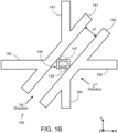
- FIG. 1A illustrates an example array 100 of qubits for a qubit system not according to the claimed invention.
- the array 100 includes multiple qubits, e.g., qubits 110-140, arranged in multiple rows, e.g., a first row ROW1 and a second row ROW2, and multiple columns, e.g., a first column COL1 and a second column COL2.
- the numbers of qubits, rows, and columns are not limited to the numbers illustrated in FIG. 1A and can include any suitable numbers of qubits, rows, and columns in various implementations.
- the qubits 110-140 can be any suitable types of qubits including Xmon qubits, transmon qubits, fluxmon qubits, and spin qubits, among others.
- the qubits 110-140 can be differential qubits. As such, none of the nodes of the qubits 110-140 shares a common ground with another node of any of the qubits.
- Each qubit of the qubits 110-140 can include two electrodes arranged in parallel.
- the first qubit 110 can include a first electrode 111 and a second electrode 112
- the second qubit 120 can include a first electrode 121 and a second electrode 122
- the third qubit 130 can include a first electrode 131 and a second electrode 132
- the fourth qubit 140 can include a first electrode 141 and a second electrode 142.
- the second qubit 120 or the third qubit 130 may be identified as the "nearest neighbor" qubit of the first qubit 110.
- the fourth qubit 140 that is diagonally located from the first qubit 110 may be identified as the "next nearest neighbor" qubit of the first qubit 110.
- the first qubit 110 or the fourth qubit 140 may be identified as the "nearest neighbor” qubit of the second qubit 120.
- the third qubit 130 that is diagonally located from the second qubit 120 may be identified as the "next nearest neighbor” qubit of the second qubit 120.
- the qubits 110-140 are not coupled to common ground. That is, electrodes of each qubit of the qubits 110-140 are coupled to different nodes that have respective potential values.
- the second electrode 112 of the first qubit 110 is coupled to a first node that has a first potential value and the second electrode 142 of the fourth qubit 140 is coupled to a second node rather than the second electrode 112 and the second electrode 142 being coupled to the common ground.
- Each qubit includes multiple co-planar waveguide arms (e.g., 151-154, 161-164, 171-174, 181-184) connected to the electrodes and separated from a ground plane 190. These co-planar waveguide arms will be explained in more detail later.
- each qubit of the qubits 110-140 can be coupled to four co-planar waveguide arms.
- the first electrode 111 of the first qubit 110 can be coupled to the co-planar waveguide arms 151, 152 and the second electrode 112 of the first qubit 110 can be coupled to the co-planar waveguide arms 153, 154.
- the co-planar waveguide arms 151, 152 can extend along orthogonal directions and the co-planar waveguide arms 153, 154 can extend along orthogonal directions. In some other implementations, the co-planar waveguide arms 151, 152 can extend along non-orthogonal directions and the co-planar waveguide arms 153, 154 can extend along non-orthogonal directions.
- the second electrode 121 of the second qubit 120 can be coupled to the co-planar waveguide arms 161, 162 and the second electrode 122 of the second qubit 120 can be coupled to the co-planar waveguide arms 163, 164.
- the co-planar waveguide arms 161, 162 can extend along orthogonal directions and the co-planar waveguide arms 163, 164 can extend along orthogonal directions.
- the co-planar waveguide arms 161, 162 can extend along non-orthogonal directions and the co-planar waveguide arms 163, 164 can extend along non-orthogonal directions.
- the first electrode 131 of the third qubit 130 can be coupled to the co-planar waveguide arms 171, 172 and the second electrode 132 of the third qubit 130 can be coupled to the co-planar waveguide arms 173, 174.
- the co-planar waveguide arms 171, 172 can extend along orthogonal directions and the co-planar waveguide arms 173, 174 can extend along orthogonal directions.
- the co-planar waveguide arms 171, 172 can extend along non-orthogonal directions and the co-planar waveguide arms 173, 174 can extend along non-orthogonal directions.
- the first electrode 141 of the fourth qubit 140 can be coupled to the co-planar waveguide arms 181, 182 and the second electrode 142 of the fourth qubit 140 can be coupled to the co-planar waveguide arms 183, 184.
- the co-planar waveguide arms 181, 182 can extend along orthogonal directions and the co-planar waveguide arms 183, 184 can extend along orthogonal directions.
- the co-planar waveguide arms 181, 182 can extend along non-orthogonal directions and the co-planar waveguide arms 183, 184 can extend along non-orthogonal directions.
- the qubits 110-140 of the array 100 may be surrounded by the ground plane 190.
- the electrodes and co-planar waveguides may be separated from the ground plane 190 by gaps 195 which expose a substrate surface, e.g., a substrate surface on which the electrodes, co-planar waveguides and ground plane are formed.
- the substrate may include a dielectric substrate such as, e.g., silicon or sapphire.
- the electrodes, the co-planar waveguides and the ground plane may be formed from a superconductor material that exhibits superconducting properties at temperatures at or below a critical temperature, such as aluminum, niobium, or titanium nitride. Other superconductors may be used as well.
- the qubits and the co-planar waveguides are located in a different plane from a ground plane.
- the ground plane can be formed in parallel to the qubit plane.
- the ground plane can be coupled to the qubit plane through interconnectors, e.g., superconducting interconnectors.
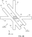
- FIG. 1B illustrates a SQUID 145 of a qubit 140 in the array 100 described with reference to FIG. 1A .
- the fourth qubit 140 includes the SQUID 145 that is located between the first electrode 141 and the second electrode 142.
- the SQUID 145 includes a first junction 147 and a second junction 149. Each of the first junction 147 and the second junction 149 is coupled to both the first electrode 141 and the second electrode 142.
- the junctions 147, 149 can be Josephson junctions.
- the qubit array 100 may be used to implement quantum computation algorithms.
- these algorithms may require coupling between nearest neighbor qubits, e.g., qubits that are closest together in adjacent rows or adjacent columns of the array, such as coupling between qubit 110 and qubit 120, or between qubit 110 and qubit 130.
- charge present in one qubit may lead to charge induced in another qubit to which coupling is not desired.
- charge present in qubit 110 may lead to undesired charge in, and thus parasitic capacitive coupling with, a next nearest neighbor qubit on the array diagonals, such as qubit 140.
- parasitic coupling may adversely affect the operation of the algorithm and the quantum computational system as a whole.
- the parasitic coupling is described in greater detail with reference to FIG. 1C .
- two electrodes of one qubit may be floating. That is, different AC voltages can be respectively applied to two electrodes of one qubit.
- a first AC voltage can be applied to the first electrode 111 and a second AC voltage can be applied to the second electrode 112.
- the first AC voltage can have a higher magnitude than the second AC voltage.
- the second AC voltage can have a higher magnitude than the first AC voltage.
- different AC voltages are respectively applied to the two electrodes of one qubit, different charges are induced in the two electrodes. This charge difference can be coupled to the differential mode of the qubit. That is, charges induced in an electrode of one qubit can induce charges in electrodes of other qubits.
- charges in the first electrode 111 of the first qubit 110 can induce charges in the first electrode 121 of the second qubit 120 or in the first electrode 141 of the fourth qubit 140.
- FIG. 1C is a schematic illustrating parasitic capacitive coupling between on-diagonal qubits within an array, such as qubit 110 and qubit 140 of FIG. 1A .
- the qubits 110-140 are not coupled to common ground, when a charge is provided on an electrode (e.g., electrode 112) of the first qubit 110, a corresponding charge is induced in both electrodes (e.g., electrodes 141, 142) of the on-diagonal qubit 140.
- a distance D1 between the second electrode 112 and the first electrode 141 is different from a distance D2 between the second electrode 112 and the second electrode 142, a different amount of charge is induced on each of electrode 141, 142.
- a larger charge having a greater magnitude (“Q") may be induced on electrode 141, and a smaller charge having a smaller magnitude (“q") may be induced on electrode 142.
- the coupling between the qubit 110 and the qubit 140 then scales with the charge difference between the induced charges on each of the electrodes within the on-diagonal qubit 140. That is, a first capacitance between the second electrode 112 and the first electrode 141 is different from a second capacitance between the second electrode 112 and the second electrode 142. As a result, a charge in the second electrode 112 induces a charge difference between the first electrode 141 and the second electrode 142.
- the orientation of the next nearest neighbor qubit may be modified so that there is little or no difference in charge between the electrodes of the next nearest neighbor qubit. Since the capacitive coupling scales with the difference in charge, reducing this difference may be relied on to reduce the amount of parasitic coupling.
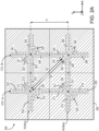
- FIG. 2A illustrates one example of an array where the orientation of the next nearest neighbor qubit is modified.
- FIG. 2A illustrates an example array 200 of qubits for a qubit system that may be used to reduce parasitic coupling to undesired qubits.
- the array 200 in FIG. 2A is the same as or similar to the array 100 in FIG. 1A except the following differences.
- the array 200 includes multiple qubits, e.g., qubits 210-240, that are arranged in multiple rows, e.g., a first row ROW1a and a second row ROW2a, and multiple columns, e.g., a first column COL1a and a second column COL2a.
- the qubits 210-240 are differential qubits.
- the numbers of qubits, rows, and columns are not limited to the numbers illustrated in FIG. 2A .
- the array 200 can include any suitable numbers of qubits, rows, and columns in various implementations.
- Each qubit of the qubits 210-240 shown in FIG. 2A is referred to as a "differential Xmon qubit.”
- the qubits 210-240 can be any suitable types of qubits including Xmon qubits, transmon qubits, fluxmon qubits, flux qubits, gatemon qubits, gmon qubits, phase qubits, and spin qubits.
- the qubits 210-240 can be any types of qubits where parasitic coupling can occur between two of those qubits.
- each qubit of the qubits 210-240 includes two electrodes arranged in parallel.
- the first qubit 210 includes a first electrode 211 and a second electrode 212
- the second qubit 220 includes a first electrode 221 and a second electrode 222
- the third qubit 230 includes a first electrode 231 and a second electrode 232
- the fourth qubit 240 includes a first electrode 241 and a second electrode 242.
- the second qubit 220 or the third qubit 230 may be identified as the "nearest neighbor" qubit of the first qubit 210.
- the fourth qubit 240 that is diagonally located from the first qubit 210 may be identified as the "next nearest neighbor" qubit of the first qubit 210.
- the first qubit 210 or the fourth qubit 240 may be identified as the "nearest neighbor” qubit of the second qubit 220.
- the third qubit 230 that is diagonally located from the second qubit 220 may be identified as the "next nearest neighbor” qubit of the second qubit 220.
- each of the qubits 210-240 also includes four co-planar waveguide arms (251-254, 261-264, 271-274, and 281-284).
- FIG. 2B illustrates a SQUID 245 of a qubit 240 in the array 200 described with reference to FIG. 2A .
- the fourth qubit 240 includes a SQUID 245 that is located between the first electrode 241 and the second electrode 242.
- the SQUID 245 includes a first junction 247 and a second junction 249.
- Each of the first junction 247 and the second junction 249 is coupled to both the first electrode 241 and the second electrode 242.
- the junctions 247, 249 can be Josephson junctions.
- the electrodes and co-planar waveguide of the qubits 210-240 are separated from a ground plane 290 by gaps 295.
- the electrodes, ground planes, and co-planar waveguide arms shown in FIG. 2A may be formed from superconductor thin films, such as aluminum, niobium, or titanium nitride, among other superconductors.
- the qubits 210-240 and ground planes 290 in FIG. 2A are formed on a dielectric substrate such as, e.g., silicon or sapphire.
- the qubits are located in a different plane from a ground plane.
- the ground plane can be formed in parallel to the qubit plane.
- the ground plane can be coupled to the qubit plane through interconnectors, e.g., superconducting interconnectors.
- electrodes of two diagonally-located qubits are arranged in perpendicular directions.
- the electrodes 211, 212 of the first qubit 210 are arranged in a first direction and the electrodes 241, 242 of the fourth qubit 240 that is a diagonally-located qubit of the first qubit 210 are arranged in a second direction that is perpendicular to the first direction such that the distance D3 between the second electrode 212 and the first electrode 241 is the same as the distance D4 between the second electrode 212 and the second electrode 242.
- the qubits 210-240 are not coupled to the same common ground. That is, electrodes of each qubit of the qubits 210-240 are coupled to different nodes that have respective potential values.
- the second electrode 212 is coupled to a first node that has a first potential value and the second electrode of the fourth 242 of the fourth qubit 240 is coupled to a second node rather than the second electrode 212 and the second electrode 242 being coupled to the common ground.
- two electrodes of one qubit may be floating. That is, different AC voltages can be respectively applied to two electrodes of one qubit.
- charge present in one qubit may lead to charge induced in another qubit to which coupling is not desired.
- charge present in the qubit 210 may lead to an induced charge in a next nearest neighbor qubit on the array diagonals, such as the qubit 240.
- parasitic coupling between the qubit 210 and the qubit 240 may be reduced and even effectively nulled.
- FIG. 2C is a schematic illustrating parasitic capacitive coupling between on-diagonal qubits within an array, such as the qubit 210 and the qubit 240 of FIG. 2A . Because the qubits are not operating in a common ground configuration, where, e.g., one electrode from each qubit is tied to the same ground potential, a same magnitude of charge (+Q) is induced in both the first electrode 241 and in the second electrode 242 of the fourth qubit 240 when a charge is provided to the electrode 212 of the first qubit 210.
- a same magnitude of charge (+Q) is induced in both the first electrode 241 and in the second electrode 242 of the fourth qubit 240 when a charge is provided to the electrode 212 of the first qubit 210.
- the differential mode of the first qubit 210 does not couple to the differential mode of the fourth qubit 240.
- the modified array of qubits shown in FIG. 2A may lead to a reduction in parasitic capacitance between qubits by about 98% compared to the array of qubits shown in FIG. 1A .
- the parasitic capacitance between the first qubit 210 and the fourth qubit 240 can be 0.33 aF.
- parasitic coupling between the second qubit 220 and the third qubit 230 can be reduced or effectively nulled.
- the parasitic capacitance between the second qubit 220 and the third qubit 230 can be 0.25 aF.
- ZZInteraction CouplingStrength 2 ⁇ 1 + ⁇ 2 ⁇ ⁇ ⁇ 1 ⁇ ⁇ + ⁇ 2
- the ZZ Error of the array 200 can be reduced by about 99%.
- the array 200 reduces or effectively nulls the parasitic capacitance between diagonally-located qubits, the array 200 does not change the coupling capacitance between one qubit and its nearest neighbor qubit comparing to the array 100.
- Table 1 shows the coupling capacitance between one qubit and its nearest qubit for the array 100 described with reference to FIG. 1A
- Table 2 shows the coupling capacitance between one qubit and its nearest qubit for the array 200 described with reference to FIG. 2A .
- Table 1 and Table 2 show that the array 200 does not change the coupling capacitance between one qubit and its nearest qubit comparing to the array 100. Since the coupling strength corresponds to coupling capacitance, the array 200 does not change coupling strength between one qubit and its nearest qubit comparing to the array 100.
- the coupling strength between the first qubit 210 and the second qubit 220 that is located the nearest from the first qubit 210 can be between 0-30 MHz and the coupling strength between the first qubit 210 and the fourth qubit 240 that is diagonally located from the first qubit 210 can be between 0-0.01MHz.
- a coupling capacitance of 0.57fF equals roughly to a coupling strength of 10 MHz at an operating frequency of 5 GHz.
- a qubit such as the qubits in array 100 or array 200
- multiple layers may be required to form the SQUID junctions. For example, a first layer of superconductor material may be deposited for form a first contact of the junctions, followed by oxidation in select regions to form the junction insulator, and then a second layer of superconductor material may be deposited to form the second contact of the junction.
- the foregoing deposition and oxidation process is typically performed without breaking vacuum. The condition that vacuum may not be broken therefore may require patterning and application of a single mask to define the features of the qubit prior to deposition and oxidation.
- an angled shadow deposition process may be used.
- a first superconductor layer is deposited by exposing the substrate and patterned mask to a first flux of superconductor material (e.g., using physical vapor deposition) at an oblique angle relative to the substrate surface. Portions of the mask may be relied on to block (i.e., effectively act as a shadow mask) deposition of the superconductor in regions where the second superconductor layer is to be performed.
- the substrate is rotated (e.g., 90 degrees) and a second superconductor layer is deposited by exposing the device and patterned mask to a second flux of superconductor material again at an oblique angle relative to the substrate surface. Portions of the mask again may be relied on to block deposition of the superconductor material, but this time from being deposited in regions where the first superconductor layer has been formed.
- An advantage of the subject matter of the present disclosure is that even though the arrangement of the on-diagonal qubits are modified relative to one another, the angled shadow deposition process still may be used. That is, there is no need to change any steps of the qubit fabrication process other than the mask design. Thus, a substantial reduction in parasitic capacitance may be achieved with no increased fabrication cost.
- quantum computational systems may include, but is not limited to, quantum computers, quantum information processing systems, quantum cryptography systems, topological quantum computers, or quantum simulators.
- quantum information and quantum data refer to information or data that is carried by, held or stored in quantum systems, where the smallest non-trivial system is a qubit, e.g., a system that defines the unit of quantum information.
- qubit encompasses all quantum systems that may be described exactly or suitably approximated as a two-level system in the corresponding context.
- Such quantum systems may include multi-level systems, e.g., with two or more levels.
- such systems can include atoms, electrons, photons, trapped or un-trapped ions, atomic nuclei, color centers, topological qubits, quantum dots, Bose-Einstein condensates, or superconducting qubits.
- the computational basis states are identified with the ground and first excited states, however it is understood that other setups where the computational states are identified with higher level excited states are possible.
- quantum memories are devices that can store quantum data for a long time with high fidelity and efficiency, e.g., light-matter interfaces where light is used for transmission and matter for storing and preserving the quantum features of quantum data such as superposition or quantum coherence.
- Quantum circuit elements include circuit elements for performing quantum processing operations. That is, the quantum circuit elements are configured to make use of quantum-mechanical phenomena, such as superposition and entanglement, to perform operations on data in a non-deterministic manner.
- Certain quantum circuit elements, such as qubits can be configured to represent and operate on information in more than one state simultaneously.
- superconducting quantum circuit elements include circuit elements such as quantum LC oscillators, qubits (e.g., flux qubits, phase qubits, or charge qubits), and superconducting quantum interference devices (SQUIDs) (e.g., RF-SQUID or DC-SQUID), among others.
- qubits e.g., flux qubits, phase qubits, or charge qubits
- SQUIDs superconducting quantum interference devices
- classical circuit elements generally process data in a deterministic manner.
- Classical circuit elements can be configured to collectively carry out instructions of a computer program by performing basic arithmetical, logical, and/or input/output operations on data, in which the data is represented in analog or digital form.
- classical circuit elements can be used to transmit data to and/or receive data from the quantum circuit elements through electrical or electromagnetic connections. Examples of classical circuit elements include circuit elements based on CMOS circuitry, rapid single flux quantum (RSFQ) devices, reciprocal quantum logic (RQL) devices and ERSFQ devices, which are an energy-efficient version of RSFQ that does not use bias resistors.
- RSFQ rapid single flux quantum
- RQL reciprocal quantum logic
- ERSFQ devices which are an energy-efficient version of RSFQ that does not use bias resistors.
- Fabrication of the circuit elements described herein can entail the deposition of one or more materials, such as superconductors, dielectrics and/or metals. Depending on the selected material, these materials can be deposited using deposition processes such as chemical vapor deposition, physical vapor deposition (e.g., evaporation or sputtering), or epitaxial techniques, among other deposition processes. Processes for fabricating circuit elements described herein can entail the removal of one or more materials from a device during fabrication. Depending on the material to be removed, the removal process can include, e.g., wet etching techniques, dry etching techniques, or lift-off processes. The materials forming the circuit elements described herein can be patterned using known lithographic techniques (e.g., photolithography or e-beam lithography).
- lithographic techniques e.g., photolithography or e-beam lithography
- the superconducting circuit elements are cooled down within a cryostat to temperatures that allow a superconductor material to exhibit superconducting properties.
- a superconductor (alternatively superconducting) material can be understood as material that exhibits superconducting properties at or below a superconducting critical temperature. Examples of superconducting material include aluminum (superconductive critical temperature of 1.2 kelvin) and niobium (superconducting critical temperature of 9.3 kelvin).
- superconducting structures such as superconducting traces and superconducting ground planes, are formed from material that exhibits superconducting properties at or below a superconducting critical temperature.
Landscapes
- Engineering & Computer Science (AREA)
- General Physics & Mathematics (AREA)
- Theoretical Computer Science (AREA)
- Physics & Mathematics (AREA)
- Mathematical Analysis (AREA)
- Computing Systems (AREA)
- Evolutionary Computation (AREA)
- Condensed Matter Physics & Semiconductors (AREA)
- Computational Mathematics (AREA)
- Mathematical Optimization (AREA)
- Pure & Applied Mathematics (AREA)
- Data Mining & Analysis (AREA)
- General Engineering & Computer Science (AREA)
- Mathematical Physics (AREA)
- Software Systems (AREA)
- Artificial Intelligence (AREA)
- Chemical & Material Sciences (AREA)
- Ceramic Engineering (AREA)
- Superconductor Devices And Manufacturing Methods Thereof (AREA)
Claims (10)
- System, umfassend eine Anordnung von Qubits, die auf einem zweidimensionalen Substrat angeordnet sind, wobei jedes Qubit der Anordnung von Qubits eine erste Elektrode (111, 121, 131, 141, 211, 221, 231, 241), die einem ersten Knoten entspricht, und eine zweite Elektrode (112, 122, 132, 142, 212, 222, 232, 242), die einem zweiten Knoten entspricht, umfasst,wobei für ein erstes Qubit (110, 210) in der Anordnung von Qubits und ein nächst benachbartes zweites Qubit (120, 220) in der Anordnung von Qubits das erste Qubit relativ zu dem zweiten Qubit so positioniert und ausgerichtet ist, dass eine auf dem ersten Qubit vorhandene Ladung eine gleiche Ladung auf jedem der ersten Knoten des zweiten Qubits und dem zweiten Knoten des zweiten Qubits induziert, sodass Koppeln zwischen dem ersten Qubit und dem zweiten Qubit verringert wird,wobei die erste Elektrode des ersten Qubits und die zweite Elektrode des ersten Qubits jeweils parallel zueinander entlang einer ersten Richtung verlaufen,wobei die erste Elektrode des zweiten Qubits und die zweite Elektrode des zweiten Qubits in einer zweiten Richtung parallel zueinander verlaufen,wobei die erste Richtung orthogonal zu der zweiten Richtung ist, wobei das erste Qubit so positioniert und ausgerichtet ist, dass eine Entfernung zwischen der ersten Elektrode des ersten Qubits und der ersten Elektrode des zweiten Qubits die gleiche ist wie die Entfernung zwischen der ersten Elektrode des ersten Qubits und der zweiten Elektrode des zweiten Qubits, undwobei keiner der Knoten eine gemeinsame Basis teilt.
- System nach Anspruch 1, wobei die Qubits in einer Vielzahl von Zeilen und einer Vielzahl von Spalten angeordnet sind, wobei sich das erste Qubit in einer anderen Zeile und einer anderen Spalte befindet als eine Zeile, beziehungsweise eine Spalte, in der sich das zweite Qubit befindet,wobei sich das erste Qubit in einer Zeile befindet, die direkt an eine Zeile angrenzt, in der sich das zweite Qubit befindet, undwobei sich das erste Qubit in einer Spalte befindet, die direkt an eine Spalte angrenzt, in der sich das zweite Qubit befindet.
- System nach einem der vorhergehenden Ansprüche, wobei das erste Qubit relativ zu einem zweiten Qubit in der Anordnung von Qubits so positioniert und ausgerichtet ist, dass eine Kapazität zwischen dem ersten Knoten des ersten Qubits und dem ersten Knoten des zweiten Qubits die gleiche ist wie die Kapazität zwischen dem ersten Knoten des ersten Qubits und dem zweiten Knoten des zweiten Qubits.
- System nach einem der vorhergehenden Ansprüche, wobei jedes Qubit in der Anordnung von Qubits einen ersten Übergang und einen zweiten Übergang umfasst, die parallel zueinander gekoppelt sind, wobei sowohl der erste Übergang als auch der zweite Übergang sowohl mit der ersten Elektrode als auch mit der zweiten Elektrode gekoppelt ist, und wobei sich der erste Übergang und der zweite Übergang jeweils zwischen der ersten Elektrode und der zweiten Elektrode befinden, und/oder wobei der erste Übergang und der zweite Übergang Josephson-Übergänge sind.
- System nach einem der vorhergehenden Ansprüche, wobei jedes Qubit in der Anordnung von Qubits einen ersten Übergang umfasst, der sowohl mit der ersten Elektrode als auch mit der zweiten Elektrode gekoppelt ist und sich zwischen der ersten Elektrode und der zweiten Elektrode befindet, und/oder wobei der erste Übergang ein Josephson-Übergang ist.
- System nach einem der vorhergehenden Ansprüche, wobei jedes Qubit vier koplanare Wellenleiterarme umfasst,wobei zwei der vier koplanaren Wellenleiter direkt mit der ersten länglichen Elektrode gekoppelt sind und sich entlang orthogonaler Richtungen erstrecken, undwobei zwei weitere der vier koplanaren Wellenleiter direkt mit der zweiten länglichen Elektrode gekoppelt sind und sich entlang orthogonaler Richtungen erstrecken.
- System nach einem der vorhergehenden Ansprüche, wobei jedes Qubit in der Anordnung von Qubits eine Supraleiter-Dünnfilm umfasst, der die erste Elektrode und die zweite Elektrode bildet, und/oder wobei der Supraleiter-Dünnfilm Aluminium, Niob oder Titannitrid umfasst.
- System nach einem der vorhergehenden Ansprüche, wobei eine Kopplungsstärke zwischen dem ersten Qubit und dem zweiten Qubit mehr als 0 MHz und weniger als 0,1 MHz für das erste Qubit beträgt, das auf eine Frequenz zwischen etwa 1 GHz und etwa 20 GHz abgestimmt ist.
- System nach einem der vorhergehenden Ansprüche, wobei die Kopplungsstärke zwischen dem ersten Qubit und einem Qubit, das dem ersten Qubit am nächsten ist, mehr als 0 MHz und weniger als 30 MHz für das erste Qubit beträgt, das auf eine Frequenz zwischen etwa 1 GHz und etwa 20 GHz abgestimmt ist.
- System nach einem der vorhergehenden Ansprüche, ferner umfassend:einer Grundebene,wobei die Grundebene eine unterschiedliche Ebene zu einer Qubit-Ebene ist, in der sich die Qubits der Anordnung von Qubits befinden.
Applications Claiming Priority (1)
| Application Number | Priority Date | Filing Date | Title |
|---|---|---|---|
| PCT/US2018/024356 WO2019190460A1 (en) | 2018-03-26 | 2018-03-26 | Reducing parasitic capacitance in a qubit system |
Publications (2)
| Publication Number | Publication Date |
|---|---|
| EP3776390A1 EP3776390A1 (de) | 2021-02-17 |
| EP3776390B1 true EP3776390B1 (de) | 2025-03-05 |
Family
ID=62047027
Family Applications (1)
| Application Number | Title | Priority Date | Filing Date |
|---|---|---|---|
| EP18720059.7A Active EP3776390B1 (de) | 2018-03-26 | 2018-03-26 | Verringerung der parasitären kapazität in einem qubit-system |
Country Status (7)
| Country | Link |
|---|---|
| US (2) | US11672188B2 (de) |
| EP (1) | EP3776390B1 (de) |
| JP (1) | JP7077419B2 (de) |
| CN (2) | CN111868757B (de) |
| AU (1) | AU2018415721B2 (de) |
| CA (1) | CA3093358A1 (de) |
| WO (1) | WO2019190460A1 (de) |
Families Citing this family (11)
| Publication number | Priority date | Publication date | Assignee | Title |
|---|---|---|---|---|
| US10720563B1 (en) * | 2018-11-13 | 2020-07-21 | Google Llc | Quantum processor design to increase control footprint |
| WO2021245949A1 (ja) * | 2020-06-05 | 2021-12-09 | 日本電気株式会社 | 量子デバイス及び量子計算機 |
| US11223347B1 (en) * | 2020-12-03 | 2022-01-11 | International Business Machines Corporation | All microwave ZZ control |
| US12016113B2 (en) * | 2020-12-22 | 2024-06-18 | Intel Corporation | Mitigating PDN induced RF interference using a stepped impedance filter |
| CN118339566A (zh) | 2021-06-11 | 2024-07-12 | 西克公司 | 针对超导量子电路的通量偏置的系统和方法 |
| CN115701272B (zh) * | 2021-07-30 | 2025-08-08 | 本源量子计算科技(合肥)股份有限公司 | 一种量子芯片及其制备方法、一种量子计算机 |
| EP4328809B1 (de) * | 2021-07-30 | 2025-10-29 | Origin Quantum Computing Technology (Hefei) Co., Ltd | Quantenschaltung, quantenchip und quantencomputer |
| US12118433B2 (en) | 2021-12-15 | 2024-10-15 | International Business Machines Corporation | Space-saving coupler arm arrangement for superconducting qubits |
| US11736091B2 (en) | 2021-12-20 | 2023-08-22 | International Business Machines Corporation | Baseband filter for current-mode signal path |
| WO2024086946A1 (en) * | 2022-10-28 | 2024-05-02 | Anyon Systems Inc. | Qubit circuits and methods of operation for reduced crosstalk |
| KR102910435B1 (ko) * | 2023-12-29 | 2026-01-09 | (재)한국나노기술원 | 초전도 양자큐비트 소자 및 그 제조방법 |
Family Cites Families (21)
| Publication number | Priority date | Publication date | Assignee | Title |
|---|---|---|---|---|
| JPS60141448U (ja) | 1984-02-29 | 1985-09-19 | 京セラ株式会社 | セラミツク製ヘツドを有する内燃機関用ピストンの構造 |
| JPH0673384B2 (ja) | 1984-08-15 | 1994-09-14 | 日本電気株式会社 | 超伝導集積回路接続パッド |
| JPS6441879A (en) * | 1987-08-07 | 1989-02-14 | Hitachi Ltd | Superconductive quantum interferometer |
| JP4180210B2 (ja) | 1999-12-03 | 2008-11-12 | 日本ペイント株式会社 | 自動車用内装材 |
| JP2003158306A (ja) | 2001-11-21 | 2003-05-30 | National Institute Of Advanced Industrial & Technology | 超伝導配線及びその作製方法 |
| JP2004235542A (ja) | 2003-01-31 | 2004-08-19 | Sharp Corp | クロストークノイズを低減するバス配線を備える電気回路装置、電気回路装置のバス配線の配線方法、電気回路装置のバス配線の配線システム |
| US20040184072A1 (en) * | 2003-03-19 | 2004-09-23 | Jacobsen Dana A. | Storing and accessing thumbnail images corresponding to print jobs |
| US7533068B2 (en) | 2004-12-23 | 2009-05-12 | D-Wave Systems, Inc. | Analog processor comprising quantum devices |
| US7639035B2 (en) | 2005-04-26 | 2009-12-29 | D-Wave Systems, Inc. | Qubit state copying |
| US7624088B2 (en) | 2005-08-03 | 2009-11-24 | D-Wave Systems Inc. | Analog processor comprising quantum devices |
| WO2007085074A1 (en) * | 2006-01-27 | 2007-08-02 | D-Wave Systems, Inc. | Methods of adiabatic quantum computation |
| US7876145B2 (en) * | 2007-07-13 | 2011-01-25 | International Business Machines Corporation | Control system architecture for qubits |
| US8642998B2 (en) * | 2011-06-14 | 2014-02-04 | International Business Machines Corporation | Array of quantum systems in a cavity for quantum computing |
| US8972921B2 (en) * | 2013-03-14 | 2015-03-03 | International Business Machines Corporation | Symmetric placement of components on a chip to reduce crosstalk induced by chip modes |
| US10037493B2 (en) * | 2013-10-22 | 2018-07-31 | D-Wave Systems Inc. | Universal adiabatic quantum computing with superconducting qubits |
| US10192168B2 (en) | 2014-02-28 | 2019-01-29 | Rigetti & Co, Inc. | Processing signals in a quantum computing system |
| US9369133B2 (en) | 2014-05-29 | 2016-06-14 | Northrop Grumman Systems Corporation | Hybrid quantum circuit assembly |
| US10930836B2 (en) * | 2015-12-30 | 2021-02-23 | Google Llc | Reducing surface loss and stray coupling in quantum devices using dielectric thinning |
| CN109219822B (zh) * | 2016-04-25 | 2022-04-12 | 谷歌有限责任公司 | 用于超导通量量子比特的耦合架构 |
| US9647662B1 (en) * | 2016-06-24 | 2017-05-09 | Northrop Grumman Systems Corporation | Superconducting tunable coupler |
| NL2018253B1 (en) * | 2017-01-27 | 2018-08-07 | Univ Delft Tech | A qubit apparatus and a qubit system |
-
2018
- 2018-03-26 EP EP18720059.7A patent/EP3776390B1/de active Active
- 2018-03-26 CA CA3093358A patent/CA3093358A1/en active Pending
- 2018-03-26 AU AU2018415721A patent/AU2018415721B2/en active Active
- 2018-03-26 CN CN201880091362.2A patent/CN111868757B/zh active Active
- 2018-03-26 CN CN202410348497.XA patent/CN118364928A/zh active Pending
- 2018-03-26 JP JP2020552037A patent/JP7077419B2/ja active Active
- 2018-03-26 US US16/977,673 patent/US11672188B2/en active Active
- 2018-03-26 WO PCT/US2018/024356 patent/WO2019190460A1/en not_active Ceased
-
2023
- 2023-04-25 US US18/139,288 patent/US12069969B2/en active Active
Also Published As
| Publication number | Publication date |
|---|---|
| US20230270021A1 (en) | 2023-08-24 |
| JP7077419B2 (ja) | 2022-05-30 |
| JP2021519459A (ja) | 2021-08-10 |
| CN111868757A (zh) | 2020-10-30 |
| AU2018415721A1 (en) | 2020-09-03 |
| CN111868757B (zh) | 2024-04-16 |
| US12069969B2 (en) | 2024-08-20 |
| WO2019190460A1 (en) | 2019-10-03 |
| CA3093358A1 (en) | 2019-10-03 |
| US11672188B2 (en) | 2023-06-06 |
| US20200395405A1 (en) | 2020-12-17 |
| AU2018415721B2 (en) | 2021-09-23 |
| CN118364928A (zh) | 2024-07-19 |
| EP3776390A1 (de) | 2021-02-17 |
Similar Documents
| Publication | Publication Date | Title |
|---|---|---|
| EP3776390B1 (de) | Verringerung der parasitären kapazität in einem qubit-system | |
| US11538976B1 (en) | Quantum processor design to increase control footprint | |
| US7613765B1 (en) | Bus architecture for quantum processing | |
| US7042005B2 (en) | Extra-substrate control system | |
| US6812484B2 (en) | Finger squid qubit device | |
| US12376501B2 (en) | Kinetic inductance devices, methods for fabricating kinetic inductance devices, and articles employing the same | |
| US6791109B2 (en) | Finger SQUID qubit device | |
| CA3085827C (en) | Transmission line resonator coupling | |
| US12239027B2 (en) | Josephson junctions with reduced stray inductance | |
| JP7317180B2 (ja) | 量子ビットシステムの寄生容量の低減 |
Legal Events
| Date | Code | Title | Description |
|---|---|---|---|
| STAA | Information on the status of an ep patent application or granted ep patent |
Free format text: STATUS: UNKNOWN |
|
| STAA | Information on the status of an ep patent application or granted ep patent |
Free format text: STATUS: THE INTERNATIONAL PUBLICATION HAS BEEN MADE |
|
| PUAI | Public reference made under article 153(3) epc to a published international application that has entered the european phase |
Free format text: ORIGINAL CODE: 0009012 |
|
| STAA | Information on the status of an ep patent application or granted ep patent |
Free format text: STATUS: REQUEST FOR EXAMINATION WAS MADE |
|
| 17P | Request for examination filed |
Effective date: 20200828 |
|
| AK | Designated contracting states |
Kind code of ref document: A1 Designated state(s): AL AT BE BG CH CY CZ DE DK EE ES FI FR GB GR HR HU IE IS IT LI LT LU LV MC MK MT NL NO PL PT RO RS SE SI SK SM TR |
|
| AX | Request for extension of the european patent |
Extension state: BA ME |
|
| DAV | Request for validation of the european patent (deleted) | ||
| DAX | Request for extension of the european patent (deleted) | ||
| STAA | Information on the status of an ep patent application or granted ep patent |
Free format text: STATUS: EXAMINATION IS IN PROGRESS |
|
| 17Q | First examination report despatched |
Effective date: 20220926 |
|
| REG | Reference to a national code |
Ref country code: DE Ref legal event code: R079 Free format text: PREVIOUS MAIN CLASS: G06N0099000000 Ipc: G06N0010400000 Ref country code: DE Ref legal event code: R079 Ref document number: 602018079785 Country of ref document: DE Free format text: PREVIOUS MAIN CLASS: G06N0099000000 Ipc: G06N0010400000 |
|
| GRAP | Despatch of communication of intention to grant a patent |
Free format text: ORIGINAL CODE: EPIDOSNIGR1 |
|
| STAA | Information on the status of an ep patent application or granted ep patent |
Free format text: STATUS: GRANT OF PATENT IS INTENDED |
|
| INTG | Intention to grant announced |
Effective date: 20240923 |
|
| RIC1 | Information provided on ipc code assigned before grant |
Ipc: G06N 10/40 20220101AFI20240913BHEP |
|
| GRAS | Grant fee paid |
Free format text: ORIGINAL CODE: EPIDOSNIGR3 |
|
| GRAA | (expected) grant |
Free format text: ORIGINAL CODE: 0009210 |
|
| STAA | Information on the status of an ep patent application or granted ep patent |
Free format text: STATUS: THE PATENT HAS BEEN GRANTED |
|
| AK | Designated contracting states |
Kind code of ref document: B1 Designated state(s): AL AT BE BG CH CY CZ DE DK EE ES FI FR GB GR HR HU IE IS IT LI LT LU LV MC MK MT NL NO PL PT RO RS SE SI SK SM TR |
|
| P01 | Opt-out of the competence of the unified patent court (upc) registered |
Free format text: CASE NUMBER: APP_4000/2025 Effective date: 20250124 |
|
| REG | Reference to a national code |
Ref country code: GB Ref legal event code: FG4D |
|
| REG | Reference to a national code |
Ref country code: CH Ref legal event code: EP |
|
| REG | Reference to a national code |
Ref country code: IE Ref legal event code: FG4D |
|
| REG | Reference to a national code |
Ref country code: DE Ref legal event code: R096 Ref document number: 602018079785 Country of ref document: DE |
|
| REG | Reference to a national code |
Ref country code: NL Ref legal event code: FP |
|
| PG25 | Lapsed in a contracting state [announced via postgrant information from national office to epo] |
Ref country code: RS Free format text: LAPSE BECAUSE OF FAILURE TO SUBMIT A TRANSLATION OF THE DESCRIPTION OR TO PAY THE FEE WITHIN THE PRESCRIBED TIME-LIMIT Effective date: 20250605 |
|
| PG25 | Lapsed in a contracting state [announced via postgrant information from national office to epo] |
Ref country code: FI Free format text: LAPSE BECAUSE OF FAILURE TO SUBMIT A TRANSLATION OF THE DESCRIPTION OR TO PAY THE FEE WITHIN THE PRESCRIBED TIME-LIMIT Effective date: 20250305 |
|
| PG25 | Lapsed in a contracting state [announced via postgrant information from national office to epo] |
Ref country code: ES Free format text: LAPSE BECAUSE OF FAILURE TO SUBMIT A TRANSLATION OF THE DESCRIPTION OR TO PAY THE FEE WITHIN THE PRESCRIBED TIME-LIMIT Effective date: 20250305 |
|
| REG | Reference to a national code |
Ref country code: LT Ref legal event code: MG9D |
|
| PG25 | Lapsed in a contracting state [announced via postgrant information from national office to epo] |
Ref country code: NO Free format text: LAPSE BECAUSE OF FAILURE TO SUBMIT A TRANSLATION OF THE DESCRIPTION OR TO PAY THE FEE WITHIN THE PRESCRIBED TIME-LIMIT Effective date: 20250605 |
|
| PG25 | Lapsed in a contracting state [announced via postgrant information from national office to epo] |
Ref country code: HR Free format text: LAPSE BECAUSE OF FAILURE TO SUBMIT A TRANSLATION OF THE DESCRIPTION OR TO PAY THE FEE WITHIN THE PRESCRIBED TIME-LIMIT Effective date: 20250305 |
|
| PG25 | Lapsed in a contracting state [announced via postgrant information from national office to epo] |
Ref country code: LV Free format text: LAPSE BECAUSE OF FAILURE TO SUBMIT A TRANSLATION OF THE DESCRIPTION OR TO PAY THE FEE WITHIN THE PRESCRIBED TIME-LIMIT Effective date: 20250305 |
|
| PG25 | Lapsed in a contracting state [announced via postgrant information from national office to epo] |
Ref country code: GR Free format text: LAPSE BECAUSE OF FAILURE TO SUBMIT A TRANSLATION OF THE DESCRIPTION OR TO PAY THE FEE WITHIN THE PRESCRIBED TIME-LIMIT Effective date: 20250606 Ref country code: BG Free format text: LAPSE BECAUSE OF FAILURE TO SUBMIT A TRANSLATION OF THE DESCRIPTION OR TO PAY THE FEE WITHIN THE PRESCRIBED TIME-LIMIT Effective date: 20250305 |
|
| REG | Reference to a national code |
Ref country code: AT Ref legal event code: MK05 Ref document number: 1773605 Country of ref document: AT Kind code of ref document: T Effective date: 20250305 |
|
| PG25 | Lapsed in a contracting state [announced via postgrant information from national office to epo] |
Ref country code: SE Free format text: LAPSE BECAUSE OF FAILURE TO SUBMIT A TRANSLATION OF THE DESCRIPTION OR TO PAY THE FEE WITHIN THE PRESCRIBED TIME-LIMIT Effective date: 20250305 |
|
| PG25 | Lapsed in a contracting state [announced via postgrant information from national office to epo] |
Ref country code: SM Free format text: LAPSE BECAUSE OF FAILURE TO SUBMIT A TRANSLATION OF THE DESCRIPTION OR TO PAY THE FEE WITHIN THE PRESCRIBED TIME-LIMIT Effective date: 20250305 |
|
| PG25 | Lapsed in a contracting state [announced via postgrant information from national office to epo] |
Ref country code: PT Free format text: LAPSE BECAUSE OF FAILURE TO SUBMIT A TRANSLATION OF THE DESCRIPTION OR TO PAY THE FEE WITHIN THE PRESCRIBED TIME-LIMIT Effective date: 20250707 |
|
| PG25 | Lapsed in a contracting state [announced via postgrant information from national office to epo] |
Ref country code: IT Free format text: LAPSE BECAUSE OF FAILURE TO SUBMIT A TRANSLATION OF THE DESCRIPTION OR TO PAY THE FEE WITHIN THE PRESCRIBED TIME-LIMIT Effective date: 20250305 Ref country code: PL Free format text: LAPSE BECAUSE OF FAILURE TO SUBMIT A TRANSLATION OF THE DESCRIPTION OR TO PAY THE FEE WITHIN THE PRESCRIBED TIME-LIMIT Effective date: 20250305 |
|
| PG25 | Lapsed in a contracting state [announced via postgrant information from national office to epo] |
Ref country code: AT Free format text: LAPSE BECAUSE OF FAILURE TO SUBMIT A TRANSLATION OF THE DESCRIPTION OR TO PAY THE FEE WITHIN THE PRESCRIBED TIME-LIMIT Effective date: 20250305 |
|
| PG25 | Lapsed in a contracting state [announced via postgrant information from national office to epo] |
Ref country code: CZ Free format text: LAPSE BECAUSE OF FAILURE TO SUBMIT A TRANSLATION OF THE DESCRIPTION OR TO PAY THE FEE WITHIN THE PRESCRIBED TIME-LIMIT Effective date: 20250305 Ref country code: EE Free format text: LAPSE BECAUSE OF FAILURE TO SUBMIT A TRANSLATION OF THE DESCRIPTION OR TO PAY THE FEE WITHIN THE PRESCRIBED TIME-LIMIT Effective date: 20250305 |
|
| REG | Reference to a national code |
Ref country code: CH Ref legal event code: H13 Free format text: ST27 STATUS EVENT CODE: U-0-0-H10-H13 (AS PROVIDED BY THE NATIONAL OFFICE) Effective date: 20251023 |
|
| PG25 | Lapsed in a contracting state [announced via postgrant information from national office to epo] |
Ref country code: RO Free format text: LAPSE BECAUSE OF FAILURE TO SUBMIT A TRANSLATION OF THE DESCRIPTION OR TO PAY THE FEE WITHIN THE PRESCRIBED TIME-LIMIT Effective date: 20250305 |
|
| PG25 | Lapsed in a contracting state [announced via postgrant information from national office to epo] |
Ref country code: SK Free format text: LAPSE BECAUSE OF FAILURE TO SUBMIT A TRANSLATION OF THE DESCRIPTION OR TO PAY THE FEE WITHIN THE PRESCRIBED TIME-LIMIT Effective date: 20250305 |
|
| PG25 | Lapsed in a contracting state [announced via postgrant information from national office to epo] |
Ref country code: IS Free format text: LAPSE BECAUSE OF FAILURE TO SUBMIT A TRANSLATION OF THE DESCRIPTION OR TO PAY THE FEE WITHIN THE PRESCRIBED TIME-LIMIT Effective date: 20250705 |
|
| PG25 | Lapsed in a contracting state [announced via postgrant information from national office to epo] |
Ref country code: LU Free format text: LAPSE BECAUSE OF NON-PAYMENT OF DUE FEES Effective date: 20250326 |
|
| REG | Reference to a national code |
Ref country code: DE Ref legal event code: R097 Ref document number: 602018079785 Country of ref document: DE |
|
| REG | Reference to a national code |
Ref country code: BE Ref legal event code: MM Effective date: 20250331 |
|
| PG25 | Lapsed in a contracting state [announced via postgrant information from national office to epo] |
Ref country code: MC Free format text: LAPSE BECAUSE OF FAILURE TO SUBMIT A TRANSLATION OF THE DESCRIPTION OR TO PAY THE FEE WITHIN THE PRESCRIBED TIME-LIMIT Effective date: 20250305 |
|
| PLBE | No opposition filed within time limit |
Free format text: ORIGINAL CODE: 0009261 |
|
| STAA | Information on the status of an ep patent application or granted ep patent |
Free format text: STATUS: NO OPPOSITION FILED WITHIN TIME LIMIT |
|
| PG25 | Lapsed in a contracting state [announced via postgrant information from national office to epo] |
Ref country code: DK Free format text: LAPSE BECAUSE OF FAILURE TO SUBMIT A TRANSLATION OF THE DESCRIPTION OR TO PAY THE FEE WITHIN THE PRESCRIBED TIME-LIMIT Effective date: 20250305 |
|
| REG | Reference to a national code |
Ref country code: CH Ref legal event code: L10 Free format text: ST27 STATUS EVENT CODE: U-0-0-L10-L00 (AS PROVIDED BY THE NATIONAL OFFICE) Effective date: 20260114 |
|
| PG25 | Lapsed in a contracting state [announced via postgrant information from national office to epo] |
Ref country code: BE Free format text: LAPSE BECAUSE OF NON-PAYMENT OF DUE FEES Effective date: 20250331 |
|
| PG25 | Lapsed in a contracting state [announced via postgrant information from national office to epo] |
Ref country code: CH Free format text: LAPSE BECAUSE OF NON-PAYMENT OF DUE FEES Effective date: 20250331 |
|
| PG25 | Lapsed in a contracting state [announced via postgrant information from national office to epo] |
Ref country code: IE Free format text: LAPSE BECAUSE OF NON-PAYMENT OF DUE FEES Effective date: 20250326 |
|
| 26N | No opposition filed |
Effective date: 20251208 |
|
| PGFP | Annual fee paid to national office [announced via postgrant information from national office to epo] |
Ref country code: GB Payment date: 20260327 Year of fee payment: 9 |
|
| PGFP | Annual fee paid to national office [announced via postgrant information from national office to epo] |
Ref country code: DE Payment date: 20260327 Year of fee payment: 9 |
|
| PGFP | Annual fee paid to national office [announced via postgrant information from national office to epo] |
Ref country code: NL Payment date: 20260326 Year of fee payment: 9 |
|
| PGFP | Annual fee paid to national office [announced via postgrant information from national office to epo] |
Ref country code: FR Payment date: 20260325 Year of fee payment: 9 |