EP3771750B1 - Procédé de dépôt d'un métal conducteur électrique sur au moins une partie de la surface interne d'une cavité interne d'un guide d'ondes - Google Patents
Procédé de dépôt d'un métal conducteur électrique sur au moins une partie de la surface interne d'une cavité interne d'un guide d'ondes Download PDFInfo
- Publication number
- EP3771750B1 EP3771750B1 EP20188644.7A EP20188644A EP3771750B1 EP 3771750 B1 EP3771750 B1 EP 3771750B1 EP 20188644 A EP20188644 A EP 20188644A EP 3771750 B1 EP3771750 B1 EP 3771750B1
- Authority
- EP
- European Patent Office
- Prior art keywords
- suspension
- waveguide
- electrically conductive
- conductive metal
- internal surface
- Prior art date
- Legal status (The legal status is an assumption and is not a legal conclusion. Google has not performed a legal analysis and makes no representation as to the accuracy of the status listed.)
- Active
Links
Images


Classifications
-
- H—ELECTRICITY
- H01—ELECTRIC ELEMENTS
- H01P—WAVEGUIDES; RESONATORS, LINES, OR OTHER DEVICES OF THE WAVEGUIDE TYPE
- H01P11/00—Apparatus or processes specially adapted for manufacturing waveguides or resonators, lines, or other devices of the waveguide type
- H01P11/001—Manufacturing waveguides or transmission lines of the waveguide type
- H01P11/002—Manufacturing hollow waveguides
-
- C—CHEMISTRY; METALLURGY
- C23—COATING METALLIC MATERIAL; COATING MATERIAL WITH METALLIC MATERIAL; CHEMICAL SURFACE TREATMENT; DIFFUSION TREATMENT OF METALLIC MATERIAL; COATING BY VACUUM EVAPORATION, BY SPUTTERING, BY ION IMPLANTATION OR BY CHEMICAL VAPOUR DEPOSITION, IN GENERAL; INHIBITING CORROSION OF METALLIC MATERIAL OR INCRUSTATION IN GENERAL
- C23C—COATING METALLIC MATERIAL; COATING MATERIAL WITH METALLIC MATERIAL; SURFACE TREATMENT OF METALLIC MATERIAL BY DIFFUSION INTO THE SURFACE, BY CHEMICAL CONVERSION OR SUBSTITUTION; COATING BY VACUUM EVAPORATION, BY SPUTTERING, BY ION IMPLANTATION OR BY CHEMICAL VAPOUR DEPOSITION, IN GENERAL
- C23C26/00—Coating not provided for in groups C23C2/00 - C23C24/00
-
- B—PERFORMING OPERATIONS; TRANSPORTING
- B05—SPRAYING OR ATOMISING IN GENERAL; APPLYING FLUENT MATERIALS TO SURFACES, IN GENERAL
- B05D—PROCESSES FOR APPLYING FLUENT MATERIALS TO SURFACES, IN GENERAL
- B05D3/00—Pretreatment of surfaces to which liquids or other fluent materials are to be applied; After-treatment of applied coatings, e.g. intermediate treating of an applied coating preparatory to subsequent applications of liquids or other fluent materials
- B05D3/02—Pretreatment of surfaces to which liquids or other fluent materials are to be applied; After-treatment of applied coatings, e.g. intermediate treating of an applied coating preparatory to subsequent applications of liquids or other fluent materials by baking
- B05D3/0254—After-treatment
-
- B—PERFORMING OPERATIONS; TRANSPORTING
- B05—SPRAYING OR ATOMISING IN GENERAL; APPLYING FLUENT MATERIALS TO SURFACES, IN GENERAL
- B05D—PROCESSES FOR APPLYING FLUENT MATERIALS TO SURFACES, IN GENERAL
- B05D5/00—Processes for applying liquids or other fluent materials to surfaces to obtain special surface effects, finishes or structures
- B05D5/12—Processes for applying liquids or other fluent materials to surfaces to obtain special surface effects, finishes or structures to obtain a coating with specific electrical properties
-
- B—PERFORMING OPERATIONS; TRANSPORTING
- B05—SPRAYING OR ATOMISING IN GENERAL; APPLYING FLUENT MATERIALS TO SURFACES, IN GENERAL
- B05D—PROCESSES FOR APPLYING FLUENT MATERIALS TO SURFACES, IN GENERAL
- B05D7/00—Processes, other than flocking, specially adapted for applying liquids or other fluent materials to particular surfaces or for applying particular liquids or other fluent materials
- B05D7/22—Processes, other than flocking, specially adapted for applying liquids or other fluent materials to particular surfaces or for applying particular liquids or other fluent materials to internal surfaces, e.g. of tubes
-
- B—PERFORMING OPERATIONS; TRANSPORTING
- B05—SPRAYING OR ATOMISING IN GENERAL; APPLYING FLUENT MATERIALS TO SURFACES, IN GENERAL
- B05D—PROCESSES FOR APPLYING FLUENT MATERIALS TO SURFACES, IN GENERAL
- B05D7/00—Processes, other than flocking, specially adapted for applying liquids or other fluent materials to particular surfaces or for applying particular liquids or other fluent materials
- B05D7/22—Processes, other than flocking, specially adapted for applying liquids or other fluent materials to particular surfaces or for applying particular liquids or other fluent materials to internal surfaces, e.g. of tubes
- B05D7/222—Processes, other than flocking, specially adapted for applying liquids or other fluent materials to particular surfaces or for applying particular liquids or other fluent materials to internal surfaces, e.g. of tubes of pipes
-
- C—CHEMISTRY; METALLURGY
- C23—COATING METALLIC MATERIAL; COATING MATERIAL WITH METALLIC MATERIAL; CHEMICAL SURFACE TREATMENT; DIFFUSION TREATMENT OF METALLIC MATERIAL; COATING BY VACUUM EVAPORATION, BY SPUTTERING, BY ION IMPLANTATION OR BY CHEMICAL VAPOUR DEPOSITION, IN GENERAL; INHIBITING CORROSION OF METALLIC MATERIAL OR INCRUSTATION IN GENERAL
- C23C—COATING METALLIC MATERIAL; COATING MATERIAL WITH METALLIC MATERIAL; SURFACE TREATMENT OF METALLIC MATERIAL BY DIFFUSION INTO THE SURFACE, BY CHEMICAL CONVERSION OR SUBSTITUTION; COATING BY VACUUM EVAPORATION, BY SPUTTERING, BY ION IMPLANTATION OR BY CHEMICAL VAPOUR DEPOSITION, IN GENERAL
- C23C18/00—Chemical coating by decomposition of either liquid compounds or solutions of the coating forming compounds, without leaving reaction products of surface material in the coating; Contact plating
- C23C18/02—Chemical coating by decomposition of either liquid compounds or solutions of the coating forming compounds, without leaving reaction products of surface material in the coating; Contact plating by thermal decomposition
-
- C—CHEMISTRY; METALLURGY
- C23—COATING METALLIC MATERIAL; COATING MATERIAL WITH METALLIC MATERIAL; CHEMICAL SURFACE TREATMENT; DIFFUSION TREATMENT OF METALLIC MATERIAL; COATING BY VACUUM EVAPORATION, BY SPUTTERING, BY ION IMPLANTATION OR BY CHEMICAL VAPOUR DEPOSITION, IN GENERAL; INHIBITING CORROSION OF METALLIC MATERIAL OR INCRUSTATION IN GENERAL
- C23C—COATING METALLIC MATERIAL; COATING MATERIAL WITH METALLIC MATERIAL; SURFACE TREATMENT OF METALLIC MATERIAL BY DIFFUSION INTO THE SURFACE, BY CHEMICAL CONVERSION OR SUBSTITUTION; COATING BY VACUUM EVAPORATION, BY SPUTTERING, BY ION IMPLANTATION OR BY CHEMICAL VAPOUR DEPOSITION, IN GENERAL
- C23C24/00—Coating starting from inorganic powder
- C23C24/08—Coating starting from inorganic powder by application of heat or pressure and heat
-
- H—ELECTRICITY
- H01—ELECTRIC ELEMENTS
- H01P—WAVEGUIDES; RESONATORS, LINES, OR OTHER DEVICES OF THE WAVEGUIDE TYPE
- H01P3/00—Waveguides; Transmission lines of the waveguide type
- H01P3/12—Hollow waveguides
-
- B—PERFORMING OPERATIONS; TRANSPORTING
- B05—SPRAYING OR ATOMISING IN GENERAL; APPLYING FLUENT MATERIALS TO SURFACES, IN GENERAL
- B05D—PROCESSES FOR APPLYING FLUENT MATERIALS TO SURFACES, IN GENERAL
- B05D2202/00—Metallic substrate
- B05D2202/30—Metallic substrate based on refractory metals (Ti, V, Cr, Zr, Nb, Mo, Hf, Ta, W)
- B05D2202/35—Metallic substrate based on refractory metals (Ti, V, Cr, Zr, Nb, Mo, Hf, Ta, W) based on Ti
-
- B—PERFORMING OPERATIONS; TRANSPORTING
- B05—SPRAYING OR ATOMISING IN GENERAL; APPLYING FLUENT MATERIALS TO SURFACES, IN GENERAL
- B05D—PROCESSES FOR APPLYING FLUENT MATERIALS TO SURFACES, IN GENERAL
- B05D2254/00—Tubes
- B05D2254/04—Applying the material on the interior of the tube
Definitions
- the present invention relates to a method for depositing an electrically conductive metal on at least part of the internal surface of an internal cavity of a waveguide.
- the present invention relates to the field of manufacturing waveguides. Without being limited in any way, this invention will find a particularly appropriate application when it comes to manufacturing a waveguide which has an internal cavity of small diameter and/or a complex shape, in particular tortuous.
- waveguides which are intended to transmit electromagnetic signals, and which find, more particularly, an application in the field of aeronautics or aerospace, notably in the framework of the creation of radars.
- Such waveguides can be made of a metallic material or of a polymer material. These waveguides can have various shapes, in particular complex shapes, for example tortuous shapes with a plurality of bends. In addition, these waveguides have an internal cavity whose cross section can adopt different shapes (rectangular, square, circular, elliptical or other) and different dimensions (which can range from a few tenths of a millimeter to several centimeters).
- the internal cavity of these waveguides must have an internal surface whose electrical conductivity properties are very high and whose condition is not very damaged. In particular, this internal surface must have low roughness.
- waveguides made of a titanium alloy include an internal cavity whose internal surface has electrical conductivity properties which prove insufficient for certain applications. To remedy this drawback, it was imagined to deposit an electrically conductive metal on this internal surface.
- the deposition, on this internal surface, of such an electrically conductive metal can be carried out according to a first process which consists of depositing silver electrolytically.
- This first process consists, first of all, of etching the internal surface and, then, of depositing, on the etched internal surface, a deposit of nickel by chemical means. Subsequently, an anode is positioned inside the waveguide and this waveguide is connected to a cathode. Then, we carry out a series of quenching of this waveguide in several successive baths containing silver. During these successive quenchings, an electric current is passed between the anode and the cathode, through the bath containing the silver. This results in silver being deposited on the internal surface of the waveguide by electrolysis.
- This first process has a certain number of drawbacks.
- this first process makes it possible to deposit, on the internal surface of the internal cavity of a waveguide, a layer of silver which is only of small thickness (from a few microns to 15 microns).
- this first process does not make it possible to deposit a constant thickness of silver over the entire internal surface of the internal cavity.
- edge effects appear.
- this first method consists of positioning an anode inside the internal cavity of the waveguide which strongly limits the size of the internal cavity and the complexity of the shape of the waveguides. waves capable of being treated by this first process, this while the current trend is to move towards waveguides whose section is increasingly smaller and whose shapes are more and more complex.
- This second process has similarities with the first process described above but differs from this first process in the sense that the deposit of silver takes place without current intervention.
- this second process makes it possible to deposit silver on the internal surface of an internal cavity of a waveguide which has a complex shape and/or an internal cavity of small section, this second process has, however, other disadvantages.
- the present invention is intended to remedy the drawbacks of state-of-the-art conditioning devices.
- the invention relates to a method of depositing an electrically conductive metal on at least part of the internal surface of an internal cavity of a waveguide.
- the invention is defined by the claims.
- This deposition process advantageously and appropriately allows the suspension to penetrate inside the internal cavity of a waveguide and to cover the internal surface of such an internal cavity, whatever the shape (even complex and/or tortuous) of this waveguide and the section (even very small, notably less than a millimeter) of this internal cavity.
- This deposition process also and advantageously makes it possible to avoid, as in the state of the art, introducing an anode inside the internal cavity of a waveguide.
- This deposition process makes it possible, then and consequently, on the one hand, to deposit an electrically conductive metal on the internal surface of an internal cavity of a waveguide of complex shape and, on the other hand, to reduce the size of the section of the internal cavity of the waveguides on the internal surface of which it is possible to deposit such an electrically conductive metal.
- This deposition process also and advantageously makes it possible to reduce defects and fragile phases in the layer of electrically conductive metal deposited on the internal surface of an internal cavity of a waveguide, this compared to the layers of metal electrical conductor deposited by state-of-the-art processes.
- Yet another advantage is that the deposition process makes it possible to achieve a coverage rate of the internal surface of an internal cavity of a waveguide of 100% and makes it possible to obtain a smoothing effect on such a internal surface.
- This deposition process also makes it possible to obtain metallurgical continuity between the waveguide and the layer of electrically conductive metal deposited on the internal surface of the internal cavity of this waveguide.
- the present invention relates to the field of manufacturing waveguides, more particularly metallized waveguides.
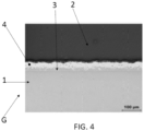
- Such a metallized waveguide G comprises a waveguide 1 (illustrated figure 1 ) which comprises an internal cavity 2 having an internal surface 3.
- Such a metallized waveguide G also comprises a layer C of an electrically conductive metal 4 deposited on at least part of this internal surface 3.
- FIG. 3 a schematic, partial and sectional view of such a metallized waveguide G obtained by implementing a process for depositing an electrically conductive metal 4 on the internal surface 3 of an internal cavity 2 of a waveguide 1, this deposition process being in accordance with the state of the art.
- this metallized waveguide G has metallurgical defects D or fragile zones Z, this at the level of the internal surface 3 of the internal cavity 2 of the waveguide 1.
- one step of this process consists of preparing a suspension S which contains at least one liquid and at least one precursor of the electrically conductive metal 4 suspended in said at least one liquid.
- said at least one liquid represents between 6 and 12% by mass of the suspension S (preferably of the order of 9.4% by mass of the suspension S) , this ensures that said at least one liquid and said at least one precursor represent 100% by mass of this suspension S.
- said at least one liquid is at least partly constituted by at least one solvent (in particular which is at least partly constituted by alcohol) and/or by at least one binder (in particular which is at least partly made up of water).
- said at least one liquid is at least partly constituted by at least one binder which is at least partly constituted by the water.
- said at least one liquid consists entirely of water.
- said at least one liquid is at least partly constituted by at least one solvent which is at least partly constituted by alcohol.
- said at least one liquid consists entirely of alcohol.
- said at least one liquid is at least partly constituted, on the one hand, by at least one solvent, in particular which is at least partly constituted by alcohol and, on the other hand , by at least one binder, in particular which is at least partly constituted by water.
- said at least one liquid is at least partly (or even entirely) constituted by a solvent constituted by alcohol and by a binder constituted by water.
- said at least one liquid may, again, be at least partly constituted by at least one adjuvant.
- said at least one liquid is at least partly (or even, and preferably, entirely) constituted, on the one hand, by at least one solvent, which is at least partly ( or even, and preferably, entirely) consisting of alcohol, and which represents between 2 and 5% by mass of the suspension S (preferably of the order of 3.7% by mass of this suspension S), and , on the other hand, by at least one binder, which is at least partly (or even, and preferably, entirely) constituted by water, and which represents between 4 and 7% by mass of the suspension S (of preferably of the order of 5.7% by mass of this suspension S).
- the precursor of the electrically conductive metal 4 then represents between 88 and 94% by mass of the suspension S (preferably of the order of 90.6% by mass of the suspension S ), this ensures that said at least one liquid (namely at least said at least one solvent and/or said at least one binder, or even said at least one adjuvant) and the precursor represent 100% by mass of this suspension S .
- the precursor of the electrically conductive metal 4 this is at least partly (or even, and preferably, entirely) constituted by at least one powder, which is fuseable, and which is at least partly (or even, and preferably, entirely) constituted by at least one alloy of the electrically conductive metal 4 and another metal.
- said electrically conductive metal 4 is at least partly (or even, and preferably, entirely) made up of silver.
- said at least one alloy mentioned above is then constituted by an alloy of silver and copper.
- a step of the process according to the invention consists of preparing a suspension S which contains at least one liquid and at least one precursor of the electrically conductive metal 4 suspended in said at least one liquid.
- the precursor of the electrically conductive metal 4 is introduced into a container, this before introducing, into this container and progressively, said at least one liquid.
- the suspension S is homogenized, in particular with stirring, more particularly using a magnetic stirrer. This suspension S is kept under stirring at least until said at least one internal surface 3 of the internal cavity 2 of the waveguide 1 is coated with the suspension S.
- a step of the method consists of coating said at least part of the internal surface 3 of the internal cavity 2 of the waveguide 1 with the suspension S.
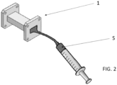
- said suspension S is injected inside the internal cavity 2 of the guide of waves 1, this as visible figure 2 and/or using a pump, syringe or the like.
- another step of the process consists, after having coated said at least part of the internal surface 3 of the internal cavity 2 of the waveguide 1 with said suspension S (in particular by injection of said suspension S inside the internal cavity 2 of the waveguide 1), in that this suspension S is withdrawn from this internal cavity 2, more particularly under the effect of gravity.
- Yet another characteristic of the invention consists in that, after having coated said at least part of the internal surface 3 of the internal cavity 2 of the waveguide 1 with said suspension S, the thickness of the conductive metal precursor electrical 4 on this internal surface 3 is preferably between 60 and 100 microns, preferably of the order of 80 microns.
- one step of the method consists of coating at least part of the internal surface 3 of the internal cavity 2 of the waveguide 1 with the suspension S.
- the entire internal surface 3 of the internal cavity 2 of the waveguide 1 is coated with the suspension S.
- Another characteristic of the method according to the invention consists in that, before coating at least part of the internal surface 3 of the internal cavity 2 of the waveguide 1 with the suspension S, at least said at least one is degreased. a part of the internal surface 3 of the internal cavity 2 of the waveguide 1, or even the entirety of this internal surface 2, or even the entirety of the waveguide 1.
- degreasing is carried out by immersion of the waveguide 1 in at least one bath (preferably in several successive baths) containing such a solvent.
- Such degreasing can be improved when carried out under ultrasound, in particular in an ultrasonic tank containing a bath such as above.
- the method consists of heat treating at least said part of the internal surface 3 of the internal cavity 2 of the waveguide 1 coated with the suspension S.
- At least this part of the internal surface 3 is heat treated (or even the entirety of this internal surface 2 coated with this suspension S, or even the entirety of the waveguide 1 coated with this suspension S) under an inert atmosphere, at least this part of the surface is treated internal 3 (or even the entirety of this internal surface 2 coated with this suspension S, or even the entirety of the waveguide 1 coated with this suspension S) under an inert gas, in particular argon.
- the internal surface 3 of the internal cavity 2 of the waveguide 1 coated with the suspension S when at least part of the internal surface 3 of the internal cavity 2 of the waveguide 1 coated with the suspension S is thermally treated (or even the entirety of this internal surface 2 coated with this suspension S, or even the entirety of the waveguide 1 coated with this suspension S), at least this part of the internal surface 3 is heated (or even the entirety of this internal surface 2 coated with this suspension S, or even again the entire waveguide 1 coated with this suspension S) and/or this suspension S at a temperature greater than or equal to the melting temperature of said at least one precursor of the electrically conductive metal 4.
- this heating is preferably carried out under an inert atmosphere or under a reducing atmosphere or (and preferably) under vacuum, more particularly under secondary vacuum.
- a particular preferred embodiment then consists of ensuring this heating in observing a plateau (in particular a plateau lasting approximately one hour) at this temperature (namely at a temperature greater than or equal to the melting temperature of said at least one precursor of the electrically conductive metal 4) and/or to ensure this heating at a temperature of approximately 820°C and/or under vacuum (more particularly under secondary vacuum).
- a preferred embodiment consists of ensuring this heating by observing a level (in particular a level lasting approximately one hour) at this temperature (namely at a temperature greater than or equal to the melting temperature of said at least one precursor electrically conductive metal 4), at a temperature of approximately 820°C, and under vacuum (more particularly under secondary vacuum).
- Such heating advantageously allows the precursor of the electrically conductive metal 4 to melt and interact with the material of the waveguide 1, more particularly by a phenomenon of dissolution and/or diffusion.
- said at least one liquid is at least partly constituted by at least one binder.
- this heating is preferably carried out under an inert atmosphere or under a reducing atmosphere or (and preferably) under vacuum, more particularly under secondary vacuum.
- a particular preferred embodiment then consists of ensuring this heating by observing a level (in particular a level lasting approximately one hour) at this temperature (namely at a temperature greater than or equal to the debinding temperature of the binder) and/or to ensure this heating at a temperature of approximately 500°C and/or under vacuum (more particularly under secondary vacuum).
- a preferred embodiment consists of ensuring this heating by observing a level (in particular a level lasting approximately one hour) at this temperature (namely at a temperature greater than or equal to the debinding temperature of the binder), at a temperature of approximately 500°C, and under vacuum (more particularly under secondary vacuum).
- the heating is provided inside an oven.
- Another preferred step of the method consists in that, after heating, the cooling of at least the waveguide 1 is ensured, this with the inertia of the oven.
- waveguide 1 is at least partly constituted by a titanium alloy.
- a preferred mode also relates to a method of manufacturing a metallized waveguide G comprising (as mentioned above), on the one hand, a waveguide 1 which comprises an internal cavity 2 having a surface internal 3 and, on the other hand, a layer C of an electrically conductive metal 4 deposited on at least part of this internal surface 3 (or even on the entirety of this internal surface 2, or even on the entire guide waves 1).
- This manufacturing process is characterized in that the layer C of the electrically conductive metal 4 is deposited on said at least part of the internal surface 3 of the internal cavity 2 of the waveguide 1 (or even on the entirety of this internal surface 2, or even over the entire waveguide 1), this by implementing the deposition process described above.
- a preferred mode concerns a metallized waveguide G which comprises (as described above), on the one hand, a waveguide 1 which comprises an internal cavity 2 having an internal surface 3 and, on the other hand, a layer C of an electrically conductive metal 4 deposited on at least part of this internal surface 3 (or even on the entirety of this internal surface 2, or even on the entirety of the waveguide 1).
- This metallized waveguide G is obtained by implementing the manufacturing process described above.
- this metallized waveguide G (obtained by implementing the method according to the invention) is devoid of metallurgical defects or fragile zones, this at the level of the internal surface 3 of the internal cavity 2 of the waveguide waves 1.
Landscapes
- Chemical & Material Sciences (AREA)
- Engineering & Computer Science (AREA)
- Metallurgy (AREA)
- Organic Chemistry (AREA)
- Mechanical Engineering (AREA)
- Chemical Kinetics & Catalysis (AREA)
- Materials Engineering (AREA)
- Life Sciences & Earth Sciences (AREA)
- Manufacturing & Machinery (AREA)
- Wood Science & Technology (AREA)
- Physics & Mathematics (AREA)
- Thermal Sciences (AREA)
- General Chemical & Material Sciences (AREA)
- Chemically Coating (AREA)
- Control Of Motors That Do Not Use Commutators (AREA)
- Other Surface Treatments For Metallic Materials (AREA)
Applications Claiming Priority (1)
| Application Number | Priority Date | Filing Date | Title |
|---|---|---|---|
| FR1908910A FR3099491B1 (fr) | 2019-08-02 | 2019-08-02 | Procédé de dépôt d’un métal conducteur électrique sur au moins une partie de la surface interne d’une cavité interne d’un guide d’ondes |
Publications (2)
| Publication Number | Publication Date |
|---|---|
| EP3771750A1 EP3771750A1 (fr) | 2021-02-03 |
| EP3771750B1 true EP3771750B1 (fr) | 2024-03-27 |
Family
ID=69190862
Family Applications (1)
| Application Number | Title | Priority Date | Filing Date |
|---|---|---|---|
| EP20188644.7A Active EP3771750B1 (fr) | 2019-08-02 | 2020-07-30 | Procédé de dépôt d'un métal conducteur électrique sur au moins une partie de la surface interne d'une cavité interne d'un guide d'ondes |
Country Status (6)
| Country | Link |
|---|---|
| US (1) | US11404761B2 (cg-RX-API-DMAC7.html) |
| EP (1) | EP3771750B1 (cg-RX-API-DMAC7.html) |
| JP (1) | JP2021055181A (cg-RX-API-DMAC7.html) |
| ES (1) | ES2982125T3 (cg-RX-API-DMAC7.html) |
| FR (1) | FR3099491B1 (cg-RX-API-DMAC7.html) |
| PL (1) | PL3771750T3 (cg-RX-API-DMAC7.html) |
Families Citing this family (1)
| Publication number | Priority date | Publication date | Assignee | Title |
|---|---|---|---|---|
| SE545300C2 (en) * | 2022-06-21 | 2023-06-20 | Trxmems Ab | A waveguide arrangement |
Family Cites Families (7)
| Publication number | Priority date | Publication date | Assignee | Title |
|---|---|---|---|---|
| IL86296A (en) | 1988-05-06 | 1991-12-15 | Univ Ramot | Hollow fiber waveguide and method of making it |
| US5398010A (en) * | 1992-05-07 | 1995-03-14 | Hughes Aircraft Company | Molded waveguide components having electroless plated thermoplastic members |
| FR2722304B1 (fr) * | 1994-07-06 | 1996-08-14 | Commissariat Energie Atomique | Procede de realisation de guides d'onde circulares et enterres, et dispositifs associes. |
| CA2197909A1 (en) * | 1997-03-06 | 1998-09-06 | Cindy Xing Qiu | Methods of manufacturing lightweight and low cost microwave components for high frequency operation |
| CN100349028C (zh) * | 2004-05-21 | 2007-11-14 | 日立电线株式会社 | 中空波导管及其制造方法 |
| US20060222762A1 (en) * | 2005-03-29 | 2006-10-05 | Mcevoy Kevin P | Inorganic waveguides and methods of making same |
| SE536670C2 (sv) * | 2011-08-26 | 2014-05-13 | Digital Metal Ab | Skiktbaserad tillverkning av friformade mikrokomponenter avmultimaterial |
-
2019
- 2019-08-02 FR FR1908910A patent/FR3099491B1/fr active Active
-
2020
- 2020-07-30 PL PL20188644.7T patent/PL3771750T3/pl unknown
- 2020-07-30 ES ES20188644T patent/ES2982125T3/es active Active
- 2020-07-30 EP EP20188644.7A patent/EP3771750B1/fr active Active
- 2020-07-31 US US16/944,657 patent/US11404761B2/en active Active
- 2020-07-31 JP JP2020130910A patent/JP2021055181A/ja active Pending
Also Published As
| Publication number | Publication date |
|---|---|
| US11404761B2 (en) | 2022-08-02 |
| FR3099491B1 (fr) | 2022-01-14 |
| FR3099491A1 (fr) | 2021-02-05 |
| EP3771750A1 (fr) | 2021-02-03 |
| PL3771750T3 (pl) | 2024-07-29 |
| JP2021055181A (ja) | 2021-04-08 |
| US20210036397A1 (en) | 2021-02-04 |
| ES2982125T3 (es) | 2024-10-14 |
Similar Documents
| Publication | Publication Date | Title |
|---|---|---|
| EP0212712B1 (fr) | Procédé de fabrication de corps creux, fermés et continus, corps creux obtenus et installation de mise en oeuvre dans le cas de billes creuses | |
| EP1204787B1 (fr) | Procede de nickelage en continu d'un conducteur en aluminium et dispositif correspondant | |
| EP0428458A1 (fr) | Matériau multicouche comprenant du graphite souple renforcé mécaniquement, électriquement et thermiquement par un métal et procédé de fabrication | |
| TW201740504A (zh) | 用於在基板內金屬化貫孔的方法 | |
| FR2722330A1 (fr) | Cable coaxial | |
| EP3771750A1 (fr) | Procédé de dépôt d'un métal conducteur électrique sur au moins une partie de la surface interne d'une cavité interne d'un guide d'ondes | |
| CN105873352B (zh) | 高频通信用基板及其制造方法 | |
| WO1992010010A1 (fr) | Element de contact de connecteur electrique | |
| US12446153B2 (en) | Circuit substrate and method for manufacturing the same | |
| EP1328012A1 (fr) | Procédé de fabrication d'un composant électronique incorporant un microcomposantinductif | |
| EP1060818B1 (fr) | Structures tridimensionnelles à haute porosité en alliages contenant du chrome | |
| JP6399494B2 (ja) | 金属皮膜形成品の製造方法 | |
| EP3752657B1 (fr) | Procede de metallisation de trous d'un module electronique par depot en phase liquide | |
| EP0142180B1 (fr) | Procédé de réalisation d'un corps moulé en matière plastique revêtu d'une couche métallique, et antenne plane ainsi réalisée | |
| DE19919902A1 (de) | Verfahren zur Herstellung eines Waferträgers, der insbesondere in einem Hochtemperatur-CVD-Reaktor bzw. bei einem Hochtemperatur-CVD-Verfahren unter Einsatz agressiver Gase Verwendung findet | |
| EP0140746A2 (fr) | Procédé de traitement thermique, par application d'énergie microonde, de revêtements sur supports diélectriques, en particulier de revêtements électriquement conducteurs | |
| EP1866462A2 (fr) | Electrode de traitement de surface | |
| Prokopenko et al. | Effect of ultrasonic vibrations on interface strength in composites | |
| FR2643775A1 (fr) | Procede de realisation de lignes electriquement conductrices sur substrat isolant et circuit hyperfrequence en comportant application | |
| EP2006902A2 (fr) | Procédé de réalisation d'une connexion électrique à base de nanotubes gainés individuellement | |
| EP1316974A1 (fr) | Procédé de fabrication d'un composant électronique incorporant un micro-composant inductif | |
| EP4029975A1 (en) | Nanodiamond article having a high concentration nanodiamond film and associated method of making | |
| BE649028A (cg-RX-API-DMAC7.html) | ||
| WO2023105436A1 (fr) | Procédé de fabrication d'un dispositif à guide d'ondes par fabrication additive et par polissage | |
| CN117374001A (zh) | 一种种子层沉积方法 |
Legal Events
| Date | Code | Title | Description |
|---|---|---|---|
| PUAI | Public reference made under article 153(3) epc to a published international application that has entered the european phase |
Free format text: ORIGINAL CODE: 0009012 |
|
| STAA | Information on the status of an ep patent application or granted ep patent |
Free format text: STATUS: THE APPLICATION HAS BEEN PUBLISHED |
|
| AK | Designated contracting states |
Kind code of ref document: A1 Designated state(s): AL AT BE BG CH CY CZ DE DK EE ES FI FR GB GR HR HU IE IS IT LI LT LU LV MC MK MT NL NO PL PT RO RS SE SI SK SM TR |
|
| AX | Request for extension of the european patent |
Extension state: BA ME |
|
| STAA | Information on the status of an ep patent application or granted ep patent |
Free format text: STATUS: REQUEST FOR EXAMINATION WAS MADE |
|
| 17P | Request for examination filed |
Effective date: 20210730 |
|
| RBV | Designated contracting states (corrected) |
Designated state(s): AL AT BE BG CH CY CZ DE DK EE ES FI FR GB GR HR HU IE IS IT LI LT LU LV MC MK MT NL NO PL PT RO RS SE SI SK SM TR |
|
| GRAP | Despatch of communication of intention to grant a patent |
Free format text: ORIGINAL CODE: EPIDOSNIGR1 |
|
| STAA | Information on the status of an ep patent application or granted ep patent |
Free format text: STATUS: GRANT OF PATENT IS INTENDED |
|
| RIC1 | Information provided on ipc code assigned before grant |
Ipc: H01P 11/00 20060101ALI20230914BHEP Ipc: G02B 6/00 20060101ALI20230914BHEP Ipc: C23C 26/00 20060101ALI20230914BHEP Ipc: C23C 24/08 20060101AFI20230914BHEP |
|
| INTG | Intention to grant announced |
Effective date: 20231018 |
|
| GRAS | Grant fee paid |
Free format text: ORIGINAL CODE: EPIDOSNIGR3 |
|
| GRAA | (expected) grant |
Free format text: ORIGINAL CODE: 0009210 |
|
| STAA | Information on the status of an ep patent application or granted ep patent |
Free format text: STATUS: THE PATENT HAS BEEN GRANTED |
|
| AK | Designated contracting states |
Kind code of ref document: B1 Designated state(s): AL AT BE BG CH CY CZ DE DK EE ES FI FR GB GR HR HU IE IS IT LI LT LU LV MC MK MT NL NO PL PT RO RS SE SI SK SM TR |
|
| REG | Reference to a national code |
Ref country code: GB Ref legal event code: FG4D Free format text: NOT ENGLISH |
|
| REG | Reference to a national code |
Ref country code: CH Ref legal event code: EP |
|
| REG | Reference to a national code |
Ref country code: DE Ref legal event code: R096 Ref document number: 602020027807 Country of ref document: DE |
|
| REG | Reference to a national code |
Ref country code: IE Ref legal event code: FG4D Free format text: LANGUAGE OF EP DOCUMENT: FRENCH |
|
| PG25 | Lapsed in a contracting state [announced via postgrant information from national office to epo] |
Ref country code: LT Free format text: LAPSE BECAUSE OF FAILURE TO SUBMIT A TRANSLATION OF THE DESCRIPTION OR TO PAY THE FEE WITHIN THE PRESCRIBED TIME-LIMIT Effective date: 20240327 |
|
| REG | Reference to a national code |
Ref country code: LT Ref legal event code: MG9D |
|
| PG25 | Lapsed in a contracting state [announced via postgrant information from national office to epo] |
Ref country code: GR Free format text: LAPSE BECAUSE OF FAILURE TO SUBMIT A TRANSLATION OF THE DESCRIPTION OR TO PAY THE FEE WITHIN THE PRESCRIBED TIME-LIMIT Effective date: 20240628 |
|
| REG | Reference to a national code |
Ref country code: SE Ref legal event code: TRGR |
|
| PG25 | Lapsed in a contracting state [announced via postgrant information from national office to epo] |
Ref country code: HR Free format text: LAPSE BECAUSE OF FAILURE TO SUBMIT A TRANSLATION OF THE DESCRIPTION OR TO PAY THE FEE WITHIN THE PRESCRIBED TIME-LIMIT Effective date: 20240327 Ref country code: RS Free format text: LAPSE BECAUSE OF FAILURE TO SUBMIT A TRANSLATION OF THE DESCRIPTION OR TO PAY THE FEE WITHIN THE PRESCRIBED TIME-LIMIT Effective date: 20240627 |
|
| PG25 | Lapsed in a contracting state [announced via postgrant information from national office to epo] |
Ref country code: RS Free format text: LAPSE BECAUSE OF FAILURE TO SUBMIT A TRANSLATION OF THE DESCRIPTION OR TO PAY THE FEE WITHIN THE PRESCRIBED TIME-LIMIT Effective date: 20240627 Ref country code: NO Free format text: LAPSE BECAUSE OF FAILURE TO SUBMIT A TRANSLATION OF THE DESCRIPTION OR TO PAY THE FEE WITHIN THE PRESCRIBED TIME-LIMIT Effective date: 20240627 Ref country code: LT Free format text: LAPSE BECAUSE OF FAILURE TO SUBMIT A TRANSLATION OF THE DESCRIPTION OR TO PAY THE FEE WITHIN THE PRESCRIBED TIME-LIMIT Effective date: 20240327 Ref country code: HR Free format text: LAPSE BECAUSE OF FAILURE TO SUBMIT A TRANSLATION OF THE DESCRIPTION OR TO PAY THE FEE WITHIN THE PRESCRIBED TIME-LIMIT Effective date: 20240327 Ref country code: GR Free format text: LAPSE BECAUSE OF FAILURE TO SUBMIT A TRANSLATION OF THE DESCRIPTION OR TO PAY THE FEE WITHIN THE PRESCRIBED TIME-LIMIT Effective date: 20240628 Ref country code: FI Free format text: LAPSE BECAUSE OF FAILURE TO SUBMIT A TRANSLATION OF THE DESCRIPTION OR TO PAY THE FEE WITHIN THE PRESCRIBED TIME-LIMIT Effective date: 20240327 Ref country code: BG Free format text: LAPSE BECAUSE OF FAILURE TO SUBMIT A TRANSLATION OF THE DESCRIPTION OR TO PAY THE FEE WITHIN THE PRESCRIBED TIME-LIMIT Effective date: 20240327 |
|
| REG | Reference to a national code |
Ref country code: NL Ref legal event code: FP |
|
| PG25 | Lapsed in a contracting state [announced via postgrant information from national office to epo] |
Ref country code: LV Free format text: LAPSE BECAUSE OF FAILURE TO SUBMIT A TRANSLATION OF THE DESCRIPTION OR TO PAY THE FEE WITHIN THE PRESCRIBED TIME-LIMIT Effective date: 20240327 |
|
| PG25 | Lapsed in a contracting state [announced via postgrant information from national office to epo] |
Ref country code: IS Free format text: LAPSE BECAUSE OF FAILURE TO SUBMIT A TRANSLATION OF THE DESCRIPTION OR TO PAY THE FEE WITHIN THE PRESCRIBED TIME-LIMIT Effective date: 20240727 |
|
| PG25 | Lapsed in a contracting state [announced via postgrant information from national office to epo] |
Ref country code: PT Free format text: LAPSE BECAUSE OF FAILURE TO SUBMIT A TRANSLATION OF THE DESCRIPTION OR TO PAY THE FEE WITHIN THE PRESCRIBED TIME-LIMIT Effective date: 20240729 Ref country code: SM Free format text: LAPSE BECAUSE OF FAILURE TO SUBMIT A TRANSLATION OF THE DESCRIPTION OR TO PAY THE FEE WITHIN THE PRESCRIBED TIME-LIMIT Effective date: 20240327 |
|
| REG | Reference to a national code |
Ref country code: ES Ref legal event code: FG2A Ref document number: 2982125 Country of ref document: ES Kind code of ref document: T3 Effective date: 20241014 |
|
| PG25 | Lapsed in a contracting state [announced via postgrant information from national office to epo] |
Ref country code: EE Free format text: LAPSE BECAUSE OF FAILURE TO SUBMIT A TRANSLATION OF THE DESCRIPTION OR TO PAY THE FEE WITHIN THE PRESCRIBED TIME-LIMIT Effective date: 20240327 |
|
| PG25 | Lapsed in a contracting state [announced via postgrant information from national office to epo] |
Ref country code: SK Free format text: LAPSE BECAUSE OF FAILURE TO SUBMIT A TRANSLATION OF THE DESCRIPTION OR TO PAY THE FEE WITHIN THE PRESCRIBED TIME-LIMIT Effective date: 20240327 |
|
| PG25 | Lapsed in a contracting state [announced via postgrant information from national office to epo] |
Ref country code: SM Free format text: LAPSE BECAUSE OF FAILURE TO SUBMIT A TRANSLATION OF THE DESCRIPTION OR TO PAY THE FEE WITHIN THE PRESCRIBED TIME-LIMIT Effective date: 20240327 Ref country code: SK Free format text: LAPSE BECAUSE OF FAILURE TO SUBMIT A TRANSLATION OF THE DESCRIPTION OR TO PAY THE FEE WITHIN THE PRESCRIBED TIME-LIMIT Effective date: 20240327 Ref country code: RO Free format text: LAPSE BECAUSE OF FAILURE TO SUBMIT A TRANSLATION OF THE DESCRIPTION OR TO PAY THE FEE WITHIN THE PRESCRIBED TIME-LIMIT Effective date: 20240327 Ref country code: PT Free format text: LAPSE BECAUSE OF FAILURE TO SUBMIT A TRANSLATION OF THE DESCRIPTION OR TO PAY THE FEE WITHIN THE PRESCRIBED TIME-LIMIT Effective date: 20240729 Ref country code: IS Free format text: LAPSE BECAUSE OF FAILURE TO SUBMIT A TRANSLATION OF THE DESCRIPTION OR TO PAY THE FEE WITHIN THE PRESCRIBED TIME-LIMIT Effective date: 20240727 Ref country code: EE Free format text: LAPSE BECAUSE OF FAILURE TO SUBMIT A TRANSLATION OF THE DESCRIPTION OR TO PAY THE FEE WITHIN THE PRESCRIBED TIME-LIMIT Effective date: 20240327 |
|
| REG | Reference to a national code |
Ref country code: DE Ref legal event code: R097 Ref document number: 602020027807 Country of ref document: DE |
|
| PG25 | Lapsed in a contracting state [announced via postgrant information from national office to epo] |
Ref country code: DK Free format text: LAPSE BECAUSE OF FAILURE TO SUBMIT A TRANSLATION OF THE DESCRIPTION OR TO PAY THE FEE WITHIN THE PRESCRIBED TIME-LIMIT Effective date: 20240327 |
|
| PG25 | Lapsed in a contracting state [announced via postgrant information from national office to epo] |
Ref country code: DK Free format text: LAPSE BECAUSE OF FAILURE TO SUBMIT A TRANSLATION OF THE DESCRIPTION OR TO PAY THE FEE WITHIN THE PRESCRIBED TIME-LIMIT Effective date: 20240327 |
|
| PG25 | Lapsed in a contracting state [announced via postgrant information from national office to epo] |
Ref country code: MC Free format text: LAPSE BECAUSE OF FAILURE TO SUBMIT A TRANSLATION OF THE DESCRIPTION OR TO PAY THE FEE WITHIN THE PRESCRIBED TIME-LIMIT Effective date: 20240327 |
|
| PLBE | No opposition filed within time limit |
Free format text: ORIGINAL CODE: 0009261 |
|
| STAA | Information on the status of an ep patent application or granted ep patent |
Free format text: STATUS: NO OPPOSITION FILED WITHIN TIME LIMIT |
|
| REG | Reference to a national code |
Ref country code: CH Ref legal event code: PL |
|
| 26N | No opposition filed |
Effective date: 20250103 |
|
| PG25 | Lapsed in a contracting state [announced via postgrant information from national office to epo] |
Ref country code: LU Free format text: LAPSE BECAUSE OF NON-PAYMENT OF DUE FEES Effective date: 20240730 |
|
| GBPC | Gb: european patent ceased through non-payment of renewal fee |
Effective date: 20240730 |
|
| PG25 | Lapsed in a contracting state [announced via postgrant information from national office to epo] |
Ref country code: LU Free format text: LAPSE BECAUSE OF NON-PAYMENT OF DUE FEES Effective date: 20240730 |
|
| PG25 | Lapsed in a contracting state [announced via postgrant information from national office to epo] |
Ref country code: CH Free format text: LAPSE BECAUSE OF NON-PAYMENT OF DUE FEES Effective date: 20240731 Ref country code: SI Free format text: LAPSE BECAUSE OF FAILURE TO SUBMIT A TRANSLATION OF THE DESCRIPTION OR TO PAY THE FEE WITHIN THE PRESCRIBED TIME-LIMIT Effective date: 20240327 |
|
| PG25 | Lapsed in a contracting state [announced via postgrant information from national office to epo] |
Ref country code: GB Free format text: LAPSE BECAUSE OF NON-PAYMENT OF DUE FEES Effective date: 20240730 |
|
| PG25 | Lapsed in a contracting state [announced via postgrant information from national office to epo] |
Ref country code: IE Free format text: LAPSE BECAUSE OF NON-PAYMENT OF DUE FEES Effective date: 20240730 |
|
| PGFP | Annual fee paid to national office [announced via postgrant information from national office to epo] |
Ref country code: ES Payment date: 20250811 Year of fee payment: 6 |
|
| PGFP | Annual fee paid to national office [announced via postgrant information from national office to epo] |
Ref country code: DE Payment date: 20250711 Year of fee payment: 6 |
|
| PGFP | Annual fee paid to national office [announced via postgrant information from national office to epo] |
Ref country code: TR Payment date: 20250707 Year of fee payment: 6 Ref country code: IT Payment date: 20250708 Year of fee payment: 6 |
|
| PGFP | Annual fee paid to national office [announced via postgrant information from national office to epo] |
Ref country code: BE Payment date: 20250724 Year of fee payment: 6 |
|
| PGFP | Annual fee paid to national office [announced via postgrant information from national office to epo] |
Ref country code: AT Payment date: 20250722 Year of fee payment: 6 |
|
| PGFP | Annual fee paid to national office [announced via postgrant information from national office to epo] |
Ref country code: SE Payment date: 20250729 Year of fee payment: 6 |
|
| PG25 | Lapsed in a contracting state [announced via postgrant information from national office to epo] |
Ref country code: CY Free format text: LAPSE BECAUSE OF FAILURE TO SUBMIT A TRANSLATION OF THE DESCRIPTION OR TO PAY THE FEE WITHIN THE PRESCRIBED TIME-LIMIT; INVALID AB INITIO Effective date: 20200730 |
|
| PG25 | Lapsed in a contracting state [announced via postgrant information from national office to epo] |
Ref country code: HU Free format text: LAPSE BECAUSE OF FAILURE TO SUBMIT A TRANSLATION OF THE DESCRIPTION OR TO PAY THE FEE WITHIN THE PRESCRIBED TIME-LIMIT; INVALID AB INITIO Effective date: 20200730 |
|
| REG | Reference to a national code |
Ref country code: AT Ref legal event code: UEP Ref document number: 1669961 Country of ref document: AT Kind code of ref document: T Effective date: 20240327 |
|
| PGFP | Annual fee paid to national office [announced via postgrant information from national office to epo] |
Ref country code: PL Payment date: 20260618 Year of fee payment: 7 |
|
| PGFP | Annual fee paid to national office [announced via postgrant information from national office to epo] |
Ref country code: NL Payment date: 20260630 Year of fee payment: 7 Ref country code: CZ Payment date: 20260622 Year of fee payment: 7 |
|
| PGFP | Annual fee paid to national office [announced via postgrant information from national office to epo] |
Ref country code: FR Payment date: 20260617 Year of fee payment: 7 |