EP3771070B1 - Resonant rectifier circuit - Google Patents
Resonant rectifier circuit Download PDFInfo
- Publication number
- EP3771070B1 EP3771070B1 EP19770892.8A EP19770892A EP3771070B1 EP 3771070 B1 EP3771070 B1 EP 3771070B1 EP 19770892 A EP19770892 A EP 19770892A EP 3771070 B1 EP3771070 B1 EP 3771070B1
- Authority
- EP
- European Patent Office
- Prior art keywords
- circuit
- resonance
- inverter circuit
- primary coil
- coil
- Prior art date
- Legal status (The legal status is an assumption and is not a legal conclusion. Google has not performed a legal analysis and makes no representation as to the accuracy of the status listed.)
- Active
Links
Images
Classifications
-
- H—ELECTRICITY
- H03—ELECTRONIC CIRCUITRY
- H03H—IMPEDANCE NETWORKS, e.g. RESONANT CIRCUITS; RESONATORS
- H03H7/00—Multiple-port networks comprising only passive electrical elements as network components
- H03H7/38—Impedance-matching networks
-
- H—ELECTRICITY
- H02—GENERATION; CONVERSION OR DISTRIBUTION OF ELECTRIC POWER
- H02M—APPARATUS FOR CONVERSION BETWEEN AC AND AC, BETWEEN AC AND DC, OR BETWEEN DC AND DC, AND FOR USE WITH MAINS OR SIMILAR POWER SUPPLY SYSTEMS; CONVERSION OF DC OR AC INPUT POWER INTO SURGE OUTPUT POWER; CONTROL OR REGULATION THEREOF
- H02M7/00—Conversion of AC power input into DC power output; Conversion of DC power input into AC power output
- H02M7/42—Conversion of DC power input into AC power output without possibility of reversal
- H02M7/44—Conversion of DC power input into AC power output without possibility of reversal by static converters
- H02M7/48—Conversion of DC power input into AC power output without possibility of reversal by static converters using discharge tubes with control electrode or semiconductor devices with control electrode
- H02M7/4815—Resonant converters
-
- H—ELECTRICITY
- H02—GENERATION; CONVERSION OR DISTRIBUTION OF ELECTRIC POWER
- H02M—APPARATUS FOR CONVERSION BETWEEN AC AND AC, BETWEEN AC AND DC, OR BETWEEN DC AND DC, AND FOR USE WITH MAINS OR SIMILAR POWER SUPPLY SYSTEMS; CONVERSION OF DC OR AC INPUT POWER INTO SURGE OUTPUT POWER; CONTROL OR REGULATION THEREOF
- H02M7/00—Conversion of AC power input into DC power output; Conversion of DC power input into AC power output
- H02M7/42—Conversion of DC power input into AC power output without possibility of reversal
- H02M7/44—Conversion of DC power input into AC power output without possibility of reversal by static converters
- H02M7/48—Conversion of DC power input into AC power output without possibility of reversal by static converters using discharge tubes with control electrode or semiconductor devices with control electrode
-
- H—ELECTRICITY
- H02—GENERATION; CONVERSION OR DISTRIBUTION OF ELECTRIC POWER
- H02J—ELECTRIC POWER NETWORKS; CIRCUIT ARRANGEMENTS OR SYSTEMS FOR SUPPLYING OR DISTRIBUTING ELECTRIC POWER; SYSTEMS FOR STORING ELECTRIC ENERGY
- H02J50/00—Circuit arrangements or systems for wireless supply or distribution of electric power
- H02J50/05—Circuit arrangements or systems for wireless supply or distribution of electric power using capacitive coupling
Definitions
- the present invention relates to a resonance matching circuit.
- An inverter circuit is a device that converts direct current power into alternating current.
- the inverter circuit includes a voltage type inverter circuit and a current type inverter circuit.
- the voltage type inverter circuit operates as a voltage source for a load
- the current type inverter circuit operates as a current source for a load.
- Such an inverter circuit is described in Non-Patent Document 1, for example.
- Non-Patent Document 1 describes as follows: the voltage type inverter circuit and the current type inverter circuit are combined with a resonance circuit, a series resonance circuit is preferable as a resonance circuit of the voltage type inverter circuit, and a parallel resonance circuit is preferable as a resonance circuit of the current type inverter circuit.
- Non-Patent Document 1 Masaaki Hisamoto, Yutaka Ito, Toshihiro Nomura, "High Frequency Power Supply Heating Circuit", Fuji Jihou, pp. 266-273, vol. 71, No. 5, 1998 .
- the environment of the electric field coupling unit refers to a state of contact between an electric device serving as a load and the electric field coupling unit, or a charging state of a portable terminal device or the like. Specifically, if the state of contact between the electric device and the electric field coupling unit is inappropriate, no load may be caused, and if the electric device or the like has a very large amount of charge, an overload may be caused.
- the zero-cross operation is an operation of turning on and off an inverter switch element at a timing when a current on the load side becomes zero, which is advantageous for improving inverter conversion efficiency and preventing noise generation.
- the present invention has been made in view of the above points, and relates to a resonance matching circuit that does not decrease transmission efficiency of a voltage type inverter circuit even when the resonance matching circuit is connected to a parallel resonance circuit.
- Document US 2015/326141 A1 discloses a resonance matching circuit according to the preamble of claim 1.
- the present invention it is possible to provide a resonance matching circuit that does not decrease transmission efficiency of a voltage type inverter circuit even when the resonance matching circuit is connected to a parallel resonance circuit.
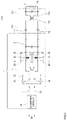
- Fig. 1 is a diagram for describing a power supply system 100 to which a resonance matching circuit according to the present embodiment is applied. However, the power supply system 100 shown in Fig. 1 does not include a load 7.
- the power supply system 100 includes a resonance matching circuit 1, a matching unit 3, an electric field coupling unit 101, and a load matching circuit 102.
- an inverter circuit 10 and the matching unit 3 constitute the resonance matching circuit 1 of the present embodiment.
- the electric field coupling unit 101 and the load matching circuit 102 are located between the resonance matching circuit 1 and the load 7, and are parts that supply power from the resonance matching circuit 1 to the load 7.
- the electric field coupling unit 101 includes capacitive elements 111 and 112 connected in series to each other.
- the load matching circuit 102 includes a primary coil 113 that constitutes an LC circuit together with the capacitive elements 111 and 112, a secondary coil 114 that forms a transformer device together with the primary coil 113, and a capacitive element 115 that constitutes an LC circuit together with the secondary coil 114.
- the resonance matching circuit 1 is a circuit used in a power supply system that supplies electric power by an electric field coupling method.
- the electric field coupling method is a method of supplying electric power from a device on a power-supply side to a device on a power-supplied side in a wireless and contactless manner. Power supply in such a method is performed in the field of portable communication terminals, self-propelled robots, and the like.
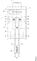
- Fig. 2 is a diagram for describing the resonance matching circuit 1 shown in Fig. 1 , and shows a configuration of the power supply system 100 shown in Fig. 1 excluding the electric field coupling unit 101 and the load matching circuit 102. The above configuration will be described below.
- the resonance matching circuit 1 includes the inverter circuit 10 and the matching unit 3 connected to the inverter circuit 10.
- the matching unit 3 includes parallel transformer devices 30 and 40 that are connected in parallel to the inverter circuit 10 and transmit a current supplied from the inverter circuit 10, and a first capacitive element 21 and a second capacitive element 22 that are located between the inverter circuit 10 and the parallel transformer devices 30 and 40 and are series capacitive elements for adjusting an input timing of a pulse current supplied by the inverter circuit 10.
- the first capacitive element 21 and the second capacitive element 22 function as a timing adjustment circuit 20 of the present embodiment.
- the resonance matching circuit 1 of the present embodiment includes the inverter circuit 10.
- a direct current voltage (Vin) is input to the inverter circuit 10 from a power supply not shown in the drawings, and the inverter circuit 10 converts the direct current voltage into a pulse current and outputs the pulse current. The generation of the pulse current is controlled by turning on and off a voltage signal.
- the inverter circuit 10 is a voltage switch/current resonance type inverter circuit that functions as a voltage source.
- the parallel transformer device 30 includes a primary coil 31 (first primary coil) and a secondary coil 32.
- a primary coil 31 first primary coil
- a secondary coil 32 When a current flows through the primary coil 31, a magnetic field is generated, and an electromotive force is generated in the secondary coil 32 by mutual induction.
- the primary coil 31 and the secondary coil 32 are wound around a core material 33 having a high dielectric constant, and boost a voltage in accordance with a ratio of the number of turns.
- the parallel transformer device 40 includes a primary coil 41 (second primary coil) and a secondary coil 42. When a current flows through the primary coil 41, a magnetic field is generated, and an electromotive force is generated in the secondary coil 42 by mutual induction.
- the primary coil 41 and the secondary coil 42 are wound around a core material 43 having a high dielectric constant, and boost a voltage in accordance with a ratio of the number of turns.
- the parallel transformer devices 30 and 40 as described above need to maintain a high voltage in the matching unit 3.
- the parallel transformer device has two systems of the parallel transformer devices 30 and 40.
- the inverter circuit 10 includes a first terminal 11 and a second terminal 12 that output electric power, and the parallel transformer devices 30 and 40 described above and the timing adjustment circuit 20 are configured as two systems. Furthermore, the first capacitive element 21, which is the series capacitive element, the primary coil 31, and the secondary coil 32 described above are used as a system on a side of the first terminal 11, and the second capacitive element 22, which is the series capacitive element, and the parallel transformer device 40 are connected to a side of the second terminal 12 similarly. In the present embodiment, the second capacitive element 22 and the parallel transformer device 40 described above are used as a system of the second terminal 12.
- the resonance matching circuit 1 forms a parallel circuit using the inverter circuit 10 as a voltage source, the first terminal 11 and the second terminal 12 are electrically connected.
- a portion of the circuit from the inverter circuit 10 to the load 7 is divided into the side of the first terminal 11 and the side of the second terminal 12, each of which is described as a "system".
- the timing adjustment circuit 20 of the present embodiment includes the first capacitive element 21 connected in series to the first terminal 11 and the second capacitive element 22 connected in series to the second terminal 12.
- the parallel transformer device 30 includes the primary coil 31 connected in series to the first capacitive element 21.
- the parallel transformer device 40 includes the primary coil 41 located between the primary coil 31 and the second capacitive element 22 and connected in series to the primary coil 31 and the second capacitive element 22.
- the parallel transformer device 40 similarly to the parallel transformer device 30, includes the secondary coil 42 that causes mutual induction with the primary coil 41. Both the primary coil 41 and the secondary coil 42 of the parallel transformer device 40 are wound around the core material 43.
- an adjustment coil 35 is provided between the primary coil 31 and the primary coil 41.
- the adjustment coil 35 is a coil that adjusts a resonance frequency of a resonance circuit A including the first capacitive element 21, the second capacitive element 22, which are series capacitors, and the primary coils 31 and 41, in accordance with a resonance frequency of a resonance circuit B including the secondary coils 32 and 42 and a parallel capacitor 5 that is parallel to the secondary coils 32 and 42.
- the adjustment coil 35 "adjusting" the resonance frequency here means that the resonance frequency of the resonance circuit A is different between a case where the adjustment coil 35 is included and a case where the adjustment coil 35 is not included.
- the resonance frequency of the resonance circuit A is adjusted so that efficiency of the inverter circuit 10 is increased.
- a circuit directly connected to the voltage source is the resonance circuit A
- a circuit magnetically connected to the resonance circuit A is the resonance circuit B.
- the first capacitive element 21, the second capacitive element 22, the primary coil 31, the adjustment coil 35, and the primary coil 41 constitute an LC circuit in the resonance circuit A
- the resonance circuit A resonates at a predetermined resonance frequency determined by characteristics or the like of each element that constitutes the LC circuit.
- the resonance circuit B the secondary coil 32, the secondary coil 42, and the parallel capacitor 5 constitute an LC circuit, and the resonance circuit B resonates at a predetermined resonance frequency.
- the adjustment coil 35 that does not contribute to mutual induction is provided for adjusting the resonance frequency of the resonance circuit A in accordance with the resonance frequency of the resonance circuit B.
- the resonance frequency is adjusted so that transmission efficiency of the inverter circuit 10 is increased.
- the inverter circuit 10 preferably operates in a so-called leading phase, in which a phase of a current leads a phase of a voltage, so that the transmission efficiency is increased.
- the adjustment coil 35 adjusts the resonance frequency of the resonance circuit A so that the phase of the current of the inverter circuit 10 leads the phase of the voltage of the inverter circuit 10.
- the resonance frequency of the resonance circuit A of the resonance matching circuit 1 is designed to be slightly lower than a target frequency
- the resonance frequency of the resonance circuit B is designed to be slightly higher than the target frequency. It is possible to achieve such a design, for example, by providing the adjustment coil 35 between the primary coil 31 and the primary coil 41.
- the resonance frequency of the resonance circuit A can be set to 1.95 MHz to 1.97 MHz with respect to the target resonance frequency of 2 MHz.
- the resonance frequency of the resonance circuit B is preferably about 2.01 MHz.
- the present embodiment is not limited to the adjustment coil 35 setting the resonance frequencies of the resonance circuit A and the resonance circuit B to the above numerical values.
- the resonance frequency may be adjusted, for example, so that the resonance frequency of the resonance circuit A is a frequency obtained by reducing the target frequency by 10%, and more preferably, the resonance frequency of the resonance circuit A is a frequency obtained by reducing the target frequency by 5%.
- the adjustment coil is not limited to being provided between the primary coil 31 and the primary coil 41 like the adjustment coil 35.
- the adjustment coil can be provided, for example, in at least one of locations between the primary coil 31 and the primary coil 41, between the first capacitive element 21 and the primary coil 31, and between the primary coil 41 and the second capacitive element 22.
- a known choke coil can be used as the adjustment coil.
- a direct current voltage is input to the inverter circuit 10 from a direct current power supply not shown in the drawings.
- the inverter circuit 10 converts the input direct current voltage into a pulse current having a rectangular wave. The conversion into the pulse current is performed so that a frequency of the pulse current coincides with the resonance frequency of the resonance circuit A.
- the pulse current is input to the timing adjustment circuit 20 of the matching unit 3.
- the timing adjustment circuit 20 the first capacitive element 21 and the second capacitive element 22 are repeatedly charged and discharged by the current supplied from the inverter circuit 10, the voltage increases during charging, and the voltage decreases during discharging.
- the inverter circuit 10 can perform a zero-cross operation by matching an output timing (on-timing) of the pulse current with a time of discharging of the first capacitive element 21 and the second capacitive element 22 (immediately before a start of charging), and thus can prevent generation of a switching noise and an inrush current and achieve efficient operation.
- the voltage boosted by the parallel transformer devices 30 and 40 is supplied to the load 7 in a contactless manner.
- Table 1 is a table showing the transmission efficiency of the power supply system 100 under an overload.
- Table 2 is a table showing the transmission efficiency of the power supply system 100 under no load.
- “frequency” is a frequency F (MHz) of the pulse current output by the inverter circuit 10.
- "Inverter circuit input” is a voltage DCV (V) and a current DCI (A) input to the inverter circuit 10 from a direct current power supply not shown in the drawings.
- An output electric power Pout (W) is electric power output from the power supply system 100, and an input electric power Pin (W) is electric power input to the power supply system 100.
- the power supply system 100 of the present embodiment can obtain the transmission efficiency of 92.6% to 93.1% when the load 7 is relatively large.
- the transmission efficiency of the circuit in which the parallel transformer devices 30 and 40 were directly connected to the voltage type inverter circuit 10 was about 70%. From this result, it is apparent that the resonance matching circuit 1 of the present embodiment including the timing adjustment circuit 20 has an effect of improving operation efficiency of the inverter circuit 10.
- the power supply system 100 has the transmission efficiency of 0 when there is no load. However, in such a region, since the output electric power is small in the first place, the decrease in the transmission efficiency does not pose a problem.
Landscapes
- Engineering & Computer Science (AREA)
- Power Engineering (AREA)
- Computer Networks & Wireless Communication (AREA)
- Inverter Devices (AREA)
Applications Claiming Priority (2)
| Application Number | Priority Date | Filing Date | Title |
|---|---|---|---|
| JP2018055133A JP7067174B2 (ja) | 2018-03-22 | 2018-03-22 | 共振整合回路 |
| PCT/JP2019/006996 WO2019181376A1 (ja) | 2018-03-22 | 2019-02-25 | 共振整合回路 |
Publications (3)
| Publication Number | Publication Date |
|---|---|
| EP3771070A1 EP3771070A1 (en) | 2021-01-27 |
| EP3771070A4 EP3771070A4 (en) | 2021-04-07 |
| EP3771070B1 true EP3771070B1 (en) | 2022-07-20 |
Family
ID=67987055
Family Applications (1)
| Application Number | Title | Priority Date | Filing Date |
|---|---|---|---|
| EP19770892.8A Active EP3771070B1 (en) | 2018-03-22 | 2019-02-25 | Resonant rectifier circuit |
Country Status (6)
| Country | Link |
|---|---|
| US (1) | US11239815B2 (https=) |
| EP (1) | EP3771070B1 (https=) |
| JP (1) | JP7067174B2 (https=) |
| KR (1) | KR102411984B1 (https=) |
| CN (1) | CN111886776B (https=) |
| WO (1) | WO2019181376A1 (https=) |
Families Citing this family (2)
| Publication number | Priority date | Publication date | Assignee | Title |
|---|---|---|---|---|
| JP7342730B2 (ja) * | 2020-02-14 | 2023-09-12 | 株式会社デンソー | 無線給電装置 |
| EP4197878A1 (en) * | 2021-12-20 | 2023-06-21 | GTS Deutschland GmbH | Frequency generator for generating a working frequency for a rail contact of an axle counter, axle counter and method for generating a working frequency for a rail contact of an axle counter |
Family Cites Families (9)
| Publication number | Priority date | Publication date | Assignee | Title |
|---|---|---|---|---|
| JP5415780B2 (ja) * | 2009-02-20 | 2014-02-12 | 健一 原川 | 電力供給システム、及びそのための可動体と固定体 |
| RU2596606C2 (ru) * | 2011-08-16 | 2016-09-10 | Конинклейке Филипс Н.В. | Динамическая резонансная согласующая схема для беспроводных приемников энергии |
| CN104956566B (zh) * | 2013-01-29 | 2018-11-13 | 富士通株式会社 | 无线电力传输系统、受电器以及无线电力传输方法 |
| JP6098646B2 (ja) | 2013-02-06 | 2017-03-22 | 株式会社村田製作所 | トランスモジュール、受電装置および送電装置 |
| JP6301112B2 (ja) | 2013-11-15 | 2018-03-28 | 株式会社ダイヘン | 高周波電源 |
| WO2015097813A1 (ja) * | 2013-12-26 | 2015-07-02 | 三菱電機エンジニアリング株式会社 | 共振型電力伝送装置 |
| CN105379067B (zh) * | 2014-06-06 | 2018-04-03 | 株式会社村田制作所 | 电力传输系统 |
| JP6618006B2 (ja) | 2015-09-29 | 2019-12-11 | パナソニックIpマネジメント株式会社 | 無線電力伝送システムおよび送電装置 |
| JP6844253B2 (ja) * | 2016-12-27 | 2021-03-17 | 富士電機株式会社 | 電源装置、一次ブロックおよび二次ブロック |
-
2018
- 2018-03-22 JP JP2018055133A patent/JP7067174B2/ja active Active
-
2019
- 2019-02-25 WO PCT/JP2019/006996 patent/WO2019181376A1/ja not_active Ceased
- 2019-02-25 CN CN201980021143.1A patent/CN111886776B/zh active Active
- 2019-02-25 US US16/976,437 patent/US11239815B2/en active Active
- 2019-02-25 EP EP19770892.8A patent/EP3771070B1/en active Active
- 2019-02-25 KR KR1020207021505A patent/KR102411984B1/ko active Active
Also Published As
| Publication number | Publication date |
|---|---|
| WO2019181376A1 (ja) | 2019-09-26 |
| JP2019170034A (ja) | 2019-10-03 |
| EP3771070A4 (en) | 2021-04-07 |
| EP3771070A1 (en) | 2021-01-27 |
| US11239815B2 (en) | 2022-02-01 |
| KR102411984B1 (ko) | 2022-06-22 |
| CN111886776B (zh) | 2024-07-16 |
| JP7067174B2 (ja) | 2022-05-16 |
| KR20200100811A (ko) | 2020-08-26 |
| US20210119597A1 (en) | 2021-04-22 |
| CN111886776A (zh) | 2020-11-03 |
Similar Documents
| Publication | Publication Date | Title |
|---|---|---|
| KR102161826B1 (ko) | 전압 컨버터, 이를 포함하는 무선 전력 수신 장치 및 무선 전력 전송 시스템 | |
| JP5135204B2 (ja) | 非接触電力伝送システム、および該非接触電力伝送システムにおける負荷装置 | |
| US6697272B2 (en) | Contactless power transmitting system and contactless charging system | |
| US8228027B2 (en) | Wireless power transmitter with multilayer printed circuit | |
| EP2587613B1 (en) | Wireless power receiver for adjusting magnitude of wireless power | |
| US9088307B2 (en) | Non-resonant and quasi-resonant system for wireless power transmission to multiple receivers | |
| JP5550785B2 (ja) | 非接触型の誘導電力伝送システムの回路 | |
| KR101979459B1 (ko) | 무선 전력 전송 시스템, 무선 전력 수신 장치 및 무선 전력 수신 방법 | |
| US10158254B2 (en) | Resonant coupling power transmission system, resonance type power transmission device, and resonance type power reception device | |
| EP2912751B1 (en) | High power rf field effect transistor switching using dc biases | |
| EP2309620A2 (en) | Wireless power feeder and wireless power transmission system | |
| CN104247206A (zh) | 电力传输系统 | |
| US10122203B2 (en) | Wireless power system | |
| KR102145903B1 (ko) | 무선 충전 시스템의 충전 제어 장치 및 방법 | |
| US20160308393A1 (en) | Contactless power receiver and method for operating same | |
| US20210175009A1 (en) | Wireless Power Transmission with Current-Limiting Coil | |
| JP2010104159A (ja) | 受電端末、および無接点電力伝送システム | |
| EP3771070B1 (en) | Resonant rectifier circuit | |
| JP2013146141A (ja) | 受電装置、送電装置および制御装置 | |
| US20180226834A1 (en) | An Inductive Power Receiver | |
| KR20140057503A (ko) | 무선전력 수신장치 및 그의 전력 제어 방법 | |
| KR20140036953A (ko) | 무선 전력 수신 장치 및 방법, 무선 전력 전송 장치 및 방법, 무선 전력 전송 시스템 | |
| WO2018213677A1 (en) | Power limiting in a wireless power transmitter | |
| CN107074121A (zh) | 用于调协振荡系统的具有可调节的电容值的装置、振荡系统和能量传输系统 | |
| EP4589809A1 (en) | Wireless power reception device |
Legal Events
| Date | Code | Title | Description |
|---|---|---|---|
| STAA | Information on the status of an ep patent application or granted ep patent |
Free format text: STATUS: THE INTERNATIONAL PUBLICATION HAS BEEN MADE |
|
| PUAI | Public reference made under article 153(3) epc to a published international application that has entered the european phase |
Free format text: ORIGINAL CODE: 0009012 |
|
| STAA | Information on the status of an ep patent application or granted ep patent |
Free format text: STATUS: REQUEST FOR EXAMINATION WAS MADE |
|
| 17P | Request for examination filed |
Effective date: 20200812 |
|
| AK | Designated contracting states |
Kind code of ref document: A1 Designated state(s): AL AT BE BG CH CY CZ DE DK EE ES FI FR GB GR HR HU IE IS IT LI LT LU LV MC MK MT NL NO PL PT RO RS SE SI SK SM TR |
|
| AX | Request for extension of the european patent |
Extension state: BA ME |
|
| A4 | Supplementary search report drawn up and despatched |
Effective date: 20210309 |
|
| RIC1 | Information provided on ipc code assigned before grant |
Ipc: H02M 7/48 20070101ALI20210302BHEP Ipc: H02J 50/05 20160101AFI20210302BHEP |
|
| RAP3 | Party data changed (applicant data changed or rights of an application transferred) |
Owner name: SUMIDA CORPORATION |
|
| DAV | Request for validation of the european patent (deleted) | ||
| DAX | Request for extension of the european patent (deleted) | ||
| GRAP | Despatch of communication of intention to grant a patent |
Free format text: ORIGINAL CODE: EPIDOSNIGR1 |
|
| STAA | Information on the status of an ep patent application or granted ep patent |
Free format text: STATUS: GRANT OF PATENT IS INTENDED |
|
| INTG | Intention to grant announced |
Effective date: 20220405 |
|
| GRAS | Grant fee paid |
Free format text: ORIGINAL CODE: EPIDOSNIGR3 |
|
| GRAA | (expected) grant |
Free format text: ORIGINAL CODE: 0009210 |
|
| STAA | Information on the status of an ep patent application or granted ep patent |
Free format text: STATUS: THE PATENT HAS BEEN GRANTED |
|
| AK | Designated contracting states |
Kind code of ref document: B1 Designated state(s): AL AT BE BG CH CY CZ DE DK EE ES FI FR GB GR HR HU IE IS IT LI LT LU LV MC MK MT NL NO PL PT RO RS SE SI SK SM TR |
|
| REG | Reference to a national code |
Ref country code: CH Ref legal event code: EP |
|
| REG | Reference to a national code |
Ref country code: DE Ref legal event code: R096 Ref document number: 602019017266 Country of ref document: DE |
|
| REG | Reference to a national code |
Ref country code: AT Ref legal event code: REF Ref document number: 1506182 Country of ref document: AT Kind code of ref document: T Effective date: 20220815 |
|
| REG | Reference to a national code |
Ref country code: IE Ref legal event code: FG4D |
|
| REG | Reference to a national code |
Ref country code: LT Ref legal event code: MG9D |
|
| REG | Reference to a national code |
Ref country code: NL Ref legal event code: MP Effective date: 20220720 |
|
| PG25 | Lapsed in a contracting state [announced via postgrant information from national office to epo] |
Ref country code: SE Free format text: LAPSE BECAUSE OF FAILURE TO SUBMIT A TRANSLATION OF THE DESCRIPTION OR TO PAY THE FEE WITHIN THE PRESCRIBED TIME-LIMIT Effective date: 20220720 Ref country code: RS Free format text: LAPSE BECAUSE OF FAILURE TO SUBMIT A TRANSLATION OF THE DESCRIPTION OR TO PAY THE FEE WITHIN THE PRESCRIBED TIME-LIMIT Effective date: 20220720 Ref country code: PT Free format text: LAPSE BECAUSE OF FAILURE TO SUBMIT A TRANSLATION OF THE DESCRIPTION OR TO PAY THE FEE WITHIN THE PRESCRIBED TIME-LIMIT Effective date: 20221121 Ref country code: NO Free format text: LAPSE BECAUSE OF FAILURE TO SUBMIT A TRANSLATION OF THE DESCRIPTION OR TO PAY THE FEE WITHIN THE PRESCRIBED TIME-LIMIT Effective date: 20221020 Ref country code: NL Free format text: LAPSE BECAUSE OF FAILURE TO SUBMIT A TRANSLATION OF THE DESCRIPTION OR TO PAY THE FEE WITHIN THE PRESCRIBED TIME-LIMIT Effective date: 20220720 Ref country code: LV Free format text: LAPSE BECAUSE OF FAILURE TO SUBMIT A TRANSLATION OF THE DESCRIPTION OR TO PAY THE FEE WITHIN THE PRESCRIBED TIME-LIMIT Effective date: 20220720 Ref country code: LT Free format text: LAPSE BECAUSE OF FAILURE TO SUBMIT A TRANSLATION OF THE DESCRIPTION OR TO PAY THE FEE WITHIN THE PRESCRIBED TIME-LIMIT Effective date: 20220720 Ref country code: FI Free format text: LAPSE BECAUSE OF FAILURE TO SUBMIT A TRANSLATION OF THE DESCRIPTION OR TO PAY THE FEE WITHIN THE PRESCRIBED TIME-LIMIT Effective date: 20220720 Ref country code: ES Free format text: LAPSE BECAUSE OF FAILURE TO SUBMIT A TRANSLATION OF THE DESCRIPTION OR TO PAY THE FEE WITHIN THE PRESCRIBED TIME-LIMIT Effective date: 20220720 |
|
| REG | Reference to a national code |
Ref country code: AT Ref legal event code: MK05 Ref document number: 1506182 Country of ref document: AT Kind code of ref document: T Effective date: 20220720 |
|
| PG25 | Lapsed in a contracting state [announced via postgrant information from national office to epo] |
Ref country code: PL Free format text: LAPSE BECAUSE OF FAILURE TO SUBMIT A TRANSLATION OF THE DESCRIPTION OR TO PAY THE FEE WITHIN THE PRESCRIBED TIME-LIMIT Effective date: 20220720 Ref country code: IS Free format text: LAPSE BECAUSE OF FAILURE TO SUBMIT A TRANSLATION OF THE DESCRIPTION OR TO PAY THE FEE WITHIN THE PRESCRIBED TIME-LIMIT Effective date: 20221120 Ref country code: HR Free format text: LAPSE BECAUSE OF FAILURE TO SUBMIT A TRANSLATION OF THE DESCRIPTION OR TO PAY THE FEE WITHIN THE PRESCRIBED TIME-LIMIT Effective date: 20220720 Ref country code: GR Free format text: LAPSE BECAUSE OF FAILURE TO SUBMIT A TRANSLATION OF THE DESCRIPTION OR TO PAY THE FEE WITHIN THE PRESCRIBED TIME-LIMIT Effective date: 20221021 |
|
| REG | Reference to a national code |
Ref country code: DE Ref legal event code: R097 Ref document number: 602019017266 Country of ref document: DE |
|
| PG25 | Lapsed in a contracting state [announced via postgrant information from national office to epo] |
Ref country code: SM Free format text: LAPSE BECAUSE OF FAILURE TO SUBMIT A TRANSLATION OF THE DESCRIPTION OR TO PAY THE FEE WITHIN THE PRESCRIBED TIME-LIMIT Effective date: 20220720 Ref country code: RO Free format text: LAPSE BECAUSE OF FAILURE TO SUBMIT A TRANSLATION OF THE DESCRIPTION OR TO PAY THE FEE WITHIN THE PRESCRIBED TIME-LIMIT Effective date: 20220720 Ref country code: DK Free format text: LAPSE BECAUSE OF FAILURE TO SUBMIT A TRANSLATION OF THE DESCRIPTION OR TO PAY THE FEE WITHIN THE PRESCRIBED TIME-LIMIT Effective date: 20220720 Ref country code: CZ Free format text: LAPSE BECAUSE OF FAILURE TO SUBMIT A TRANSLATION OF THE DESCRIPTION OR TO PAY THE FEE WITHIN THE PRESCRIBED TIME-LIMIT Effective date: 20220720 Ref country code: AT Free format text: LAPSE BECAUSE OF FAILURE TO SUBMIT A TRANSLATION OF THE DESCRIPTION OR TO PAY THE FEE WITHIN THE PRESCRIBED TIME-LIMIT Effective date: 20220720 |
|
| PLBE | No opposition filed within time limit |
Free format text: ORIGINAL CODE: 0009261 |
|
| STAA | Information on the status of an ep patent application or granted ep patent |
Free format text: STATUS: NO OPPOSITION FILED WITHIN TIME LIMIT |
|
| PG25 | Lapsed in a contracting state [announced via postgrant information from national office to epo] |
Ref country code: SK Free format text: LAPSE BECAUSE OF FAILURE TO SUBMIT A TRANSLATION OF THE DESCRIPTION OR TO PAY THE FEE WITHIN THE PRESCRIBED TIME-LIMIT Effective date: 20220720 Ref country code: EE Free format text: LAPSE BECAUSE OF FAILURE TO SUBMIT A TRANSLATION OF THE DESCRIPTION OR TO PAY THE FEE WITHIN THE PRESCRIBED TIME-LIMIT Effective date: 20220720 |
|
| 26N | No opposition filed |
Effective date: 20230421 |
|
| PG25 | Lapsed in a contracting state [announced via postgrant information from national office to epo] |
Ref country code: AL Free format text: LAPSE BECAUSE OF FAILURE TO SUBMIT A TRANSLATION OF THE DESCRIPTION OR TO PAY THE FEE WITHIN THE PRESCRIBED TIME-LIMIT Effective date: 20220720 |
|
| PG25 | Lapsed in a contracting state [announced via postgrant information from national office to epo] |
Ref country code: SI Free format text: LAPSE BECAUSE OF FAILURE TO SUBMIT A TRANSLATION OF THE DESCRIPTION OR TO PAY THE FEE WITHIN THE PRESCRIBED TIME-LIMIT Effective date: 20220720 |
|
| PG25 | Lapsed in a contracting state [announced via postgrant information from national office to epo] |
Ref country code: MC Free format text: LAPSE BECAUSE OF FAILURE TO SUBMIT A TRANSLATION OF THE DESCRIPTION OR TO PAY THE FEE WITHIN THE PRESCRIBED TIME-LIMIT Effective date: 20220720 |
|
| REG | Reference to a national code |
Ref country code: CH Ref legal event code: PL |
|
| REG | Reference to a national code |
Ref country code: BE Ref legal event code: MM Effective date: 20230228 |
|
| PG25 | Lapsed in a contracting state [announced via postgrant information from national office to epo] |
Ref country code: LU Free format text: LAPSE BECAUSE OF NON-PAYMENT OF DUE FEES Effective date: 20230225 Ref country code: LI Free format text: LAPSE BECAUSE OF NON-PAYMENT OF DUE FEES Effective date: 20230228 Ref country code: CH Free format text: LAPSE BECAUSE OF NON-PAYMENT OF DUE FEES Effective date: 20230228 |
|
| REG | Reference to a national code |
Ref country code: IE Ref legal event code: MM4A |
|
| PG25 | Lapsed in a contracting state [announced via postgrant information from national office to epo] |
Ref country code: IE Free format text: LAPSE BECAUSE OF NON-PAYMENT OF DUE FEES Effective date: 20230225 |
|
| PG25 | Lapsed in a contracting state [announced via postgrant information from national office to epo] |
Ref country code: BE Free format text: LAPSE BECAUSE OF NON-PAYMENT OF DUE FEES Effective date: 20230228 |
|
| PG25 | Lapsed in a contracting state [announced via postgrant information from national office to epo] |
Ref country code: IT Free format text: LAPSE BECAUSE OF FAILURE TO SUBMIT A TRANSLATION OF THE DESCRIPTION OR TO PAY THE FEE WITHIN THE PRESCRIBED TIME-LIMIT Effective date: 20220720 |
|
| PG25 | Lapsed in a contracting state [announced via postgrant information from national office to epo] |
Ref country code: BG Free format text: LAPSE BECAUSE OF FAILURE TO SUBMIT A TRANSLATION OF THE DESCRIPTION OR TO PAY THE FEE WITHIN THE PRESCRIBED TIME-LIMIT Effective date: 20220720 |
|
| PG25 | Lapsed in a contracting state [announced via postgrant information from national office to epo] |
Ref country code: BG Free format text: LAPSE BECAUSE OF FAILURE TO SUBMIT A TRANSLATION OF THE DESCRIPTION OR TO PAY THE FEE WITHIN THE PRESCRIBED TIME-LIMIT Effective date: 20220720 |
|
| PG25 | Lapsed in a contracting state [announced via postgrant information from national office to epo] |
Ref country code: CY Free format text: LAPSE BECAUSE OF FAILURE TO SUBMIT A TRANSLATION OF THE DESCRIPTION OR TO PAY THE FEE WITHIN THE PRESCRIBED TIME-LIMIT; INVALID AB INITIO Effective date: 20190225 |
|
| PG25 | Lapsed in a contracting state [announced via postgrant information from national office to epo] |
Ref country code: HU Free format text: LAPSE BECAUSE OF FAILURE TO SUBMIT A TRANSLATION OF THE DESCRIPTION OR TO PAY THE FEE WITHIN THE PRESCRIBED TIME-LIMIT; INVALID AB INITIO Effective date: 20190225 |
|
| PG25 | Lapsed in a contracting state [announced via postgrant information from national office to epo] |
Ref country code: TR Free format text: LAPSE BECAUSE OF FAILURE TO SUBMIT A TRANSLATION OF THE DESCRIPTION OR TO PAY THE FEE WITHIN THE PRESCRIBED TIME-LIMIT Effective date: 20220720 |
|
| PGFP | Annual fee paid to national office [announced via postgrant information from national office to epo] |
Ref country code: GB Payment date: 20260220 Year of fee payment: 8 |
|
| PGFP | Annual fee paid to national office [announced via postgrant information from national office to epo] |
Ref country code: DE Payment date: 20260218 Year of fee payment: 8 |
|
| PGFP | Annual fee paid to national office [announced via postgrant information from national office to epo] |
Ref country code: FR Payment date: 20260218 Year of fee payment: 8 |