EP3767167A1 - Led-lichtquelle zur pflanzenlichtergänzung und lampe damit - Google Patents
Led-lichtquelle zur pflanzenlichtergänzung und lampe damit Download PDFInfo
- Publication number
- EP3767167A1 EP3767167A1 EP19886796.2A EP19886796A EP3767167A1 EP 3767167 A1 EP3767167 A1 EP 3767167A1 EP 19886796 A EP19886796 A EP 19886796A EP 3767167 A1 EP3767167 A1 EP 3767167A1
- Authority
- EP
- European Patent Office
- Prior art keywords
- led chip
- powder layer
- glue
- glue powder
- phosphors
- Prior art date
- Legal status (The legal status is an assumption and is not a legal conclusion. Google has not performed a legal analysis and makes no representation as to the accuracy of the status listed.)
- Granted
Links
Images

Classifications
-
- A—HUMAN NECESSITIES
- A01—AGRICULTURE; FORESTRY; ANIMAL HUSBANDRY; HUNTING; TRAPPING; FISHING
- A01G—HORTICULTURE; CULTIVATION OF VEGETABLES, FLOWERS, RICE, FRUIT, VINES, HOPS OR SEAWEED; FORESTRY; WATERING
- A01G7/00—Botany in general
- A01G7/04—Electric or magnetic or acoustic treatment of plants for promoting growth
- A01G7/045—Electric or magnetic or acoustic treatment of plants for promoting growth with electric lighting
-
- F—MECHANICAL ENGINEERING; LIGHTING; HEATING; WEAPONS; BLASTING
- F21—LIGHTING
- F21V—FUNCTIONAL FEATURES OR DETAILS OF LIGHTING DEVICES OR SYSTEMS THEREOF; STRUCTURAL COMBINATIONS OF LIGHTING DEVICES WITH OTHER ARTICLES, NOT OTHERWISE PROVIDED FOR
- F21V9/00—Elements for modifying spectral properties, polarisation or intensity of the light emitted, e.g. filters
- F21V9/30—Elements containing photoluminescent material distinct from or spaced from the light source
- F21V9/32—Elements containing photoluminescent material distinct from or spaced from the light source characterised by the arrangement of the photoluminescent material
-
- F—MECHANICAL ENGINEERING; LIGHTING; HEATING; WEAPONS; BLASTING
- F21—LIGHTING
- F21V—FUNCTIONAL FEATURES OR DETAILS OF LIGHTING DEVICES OR SYSTEMS THEREOF; STRUCTURAL COMBINATIONS OF LIGHTING DEVICES WITH OTHER ARTICLES, NOT OTHERWISE PROVIDED FOR
- F21V9/00—Elements for modifying spectral properties, polarisation or intensity of the light emitted, e.g. filters
- F21V9/40—Elements for modifying spectral properties, polarisation or intensity of the light emitted, e.g. filters with provision for controlling spectral properties, e.g. colour, or intensity
- F21V9/45—Elements for modifying spectral properties, polarisation or intensity of the light emitted, e.g. filters with provision for controlling spectral properties, e.g. colour, or intensity by adjustment of photoluminescent elements
-
- H—ELECTRICITY
- H10—SEMICONDUCTOR DEVICES; ELECTRIC SOLID-STATE DEVICES NOT OTHERWISE PROVIDED FOR
- H10H—INORGANIC LIGHT-EMITTING SEMICONDUCTOR DEVICES HAVING POTENTIAL BARRIERS
- H10H20/00—Individual inorganic light-emitting semiconductor devices having potential barriers, e.g. light-emitting diodes [LED]
- H10H20/80—Constructional details
- H10H20/85—Packages
- H10H20/851—Wavelength conversion means
- H10H20/8511—Wavelength conversion means characterised by their material, e.g. binder
- H10H20/8512—Wavelength conversion materials
- H10H20/8513—Wavelength conversion materials having two or more wavelength conversion materials
-
- H—ELECTRICITY
- H10—SEMICONDUCTOR DEVICES; ELECTRIC SOLID-STATE DEVICES NOT OTHERWISE PROVIDED FOR
- H10W—GENERIC PACKAGES, INTERCONNECTIONS, CONNECTORS OR OTHER CONSTRUCTIONAL DETAILS OF DEVICES COVERED BY CLASS H10
- H10W90/00—Package configurations
-
- H—ELECTRICITY
- H10—SEMICONDUCTOR DEVICES; ELECTRIC SOLID-STATE DEVICES NOT OTHERWISE PROVIDED FOR
- H10H—INORGANIC LIGHT-EMITTING SEMICONDUCTOR DEVICES HAVING POTENTIAL BARRIERS
- H10H20/00—Individual inorganic light-emitting semiconductor devices having potential barriers, e.g. light-emitting diodes [LED]
- H10H20/80—Constructional details
- H10H20/85—Packages
- H10H20/851—Wavelength conversion means
- H10H20/8511—Wavelength conversion means characterised by their material, e.g. binder
-
- H—ELECTRICITY
- H10—SEMICONDUCTOR DEVICES; ELECTRIC SOLID-STATE DEVICES NOT OTHERWISE PROVIDED FOR
- H10H—INORGANIC LIGHT-EMITTING SEMICONDUCTOR DEVICES HAVING POTENTIAL BARRIERS
- H10H20/00—Individual inorganic light-emitting semiconductor devices having potential barriers, e.g. light-emitting diodes [LED]
- H10H20/80—Constructional details
- H10H20/85—Packages
- H10H20/857—Interconnections, e.g. lead-frames, bond wires or solder balls
-
- Y—GENERAL TAGGING OF NEW TECHNOLOGICAL DEVELOPMENTS; GENERAL TAGGING OF CROSS-SECTIONAL TECHNOLOGIES SPANNING OVER SEVERAL SECTIONS OF THE IPC; TECHNICAL SUBJECTS COVERED BY FORMER USPC CROSS-REFERENCE ART COLLECTIONS [XRACs] AND DIGESTS
- Y02—TECHNOLOGIES OR APPLICATIONS FOR MITIGATION OR ADAPTATION AGAINST CLIMATE CHANGE
- Y02P—CLIMATE CHANGE MITIGATION TECHNOLOGIES IN THE PRODUCTION OR PROCESSING OF GOODS
- Y02P60/00—Technologies relating to agriculture, livestock or agroalimentary industries
- Y02P60/14—Measures for saving energy, e.g. in green houses
Definitions
- the present disclosure relates to an LED light source for supplemental lighting for plants and a lamp with the light source, and pertains to the technical field of facility agriculture lighting.
- light radiation has a regulatory effect on photosynthesis, growth and development, morphogenesis, and metabolism of plants.
- Different wavelengths of light irradiated on plants have different physiological effects on plants, and thus the weight of light of different wavelengths in photosynthesis is also different and varies depending on plant species and growth stages.
- Chlorophyll is responsible for absorption, transmission and transformation of light energy in a plant body, while carotenoids have two major functions of light energy capture and photoprotection. They play a very important role in photosynthesis.
- Chlorophyll a has maximum absorption peaks of 410 nm, 430 nm and 660 nm; and chlorophyll b has maximum absorption peaks of 430 nm, 455 nm and 640 nm.
- Carotenoids are important accessory pigments, and the light energy they absorbed is just complementary to that absorbed by chlorophyll and thus can help chlorophyll receive light energy.
- Carotenoids have an absorption band of the blue-violet light region from 400 nm to 500 nm, leucocyan has a maximum absorbance in the orange-red light region, and phycoerythrobilin has a maximum absorbance in the green light region.
- the influence of light quality in lighting conditions has attracted increasing attention.
- the ratio (R/FR) of red light to far-red light in the spectrum has an important influence on the regulation of gibberellin (CA) content in plants, plant morphogenesis, and plant height adjustment.
- CA gibberellin
- Green plants need visible light for photosynthesis during their growth.
- visible light is a kind of composite light, and different plants have different requirements for different colors of visible light during their growth process.
- the number of red LEDs or far-red LEDs in the light source needs to be increased to achieve adjustment of the R/FR ratio, so as to achieve the purpose of controlling the morphology of the plant; and the number of green LEDs needs to be increased to make up for deficiencies in the spectrum.
- multiple LED light sources of different colors are combined to achieve a light environment with various light qualities in different proportions, which is extremely inconvenient for users. If the proportions of LED light sources of different colors are wrong in the process of combination of LED light sources, it is difficult to achieve the purpose of increasing plant yield and quality.
- LED light sources in the prior art are described in CN 201180055432.7 , CN 201210414873.8 , and CN 201210375582.2 .
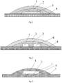
- an LED light source for supplemental lighting for plants including a substrate, an LED chip, a first glue powder layer, and a second glue powder layer; wherein, the LED chip is mounted on one surface of the substrate; the LED chip being a blue LED chip; the LED chip is covered thereon with the first glue powder layer and the second glue powder layer; the LED chip is fixed on the substrate through the first glue powder layer which is a mixture of glue and red phosphors; and the second glue powder layer covers the first glue powder layer and completely wraps the first glue powder layer; the second glue powder layer being a mixture of glue and yellow phosphors; or the second glue powder layer being a mixture of glue and infrared phosphors.
- an LED light source for supplemental lighting for plants including a substrate, an LED chip, and a first glue powder layer; wherein, the LED chip is mounted on one surface of the substrate; the LED chip being a blue LED chip; the LED chip is covered thereon with the first glue powder layer; the LED chip is fixed on the substrate through the first glue powder layer which is a mixture of glue, red phosphors and yellow phosphors, or a mixture of glue, red phosphors, and infrared phosphors.
- an LED device for supplemental lighting for plants including a substrate, an LED chip, a first glue powder layer, and a second glue powder layer; wherein, the LED chip is mounted on one surface of the substrate; the LED chip including one of a blue LED chip and an ultraviolet LED chip, or a combination thereof; the LED chip is covered thereon with the first glue powder layer and the second glue powder layer; the LED chip is fixed on the substrate through the first glue powder layer which is a mixture of glue and red phosphors; and the second glue powder layer covers the first glue powder layer and completely wraps the first glue powder layer; the second glue powder layer being a mixture of glue and infrared phosphors; or the second glue powder layer being a mixture of glue and yellow phosphors.
- an LED device for supplemental lighting for plants including a substrate, an LED chip, and a first glue powder layer; wherein, the LED chip is mounted on one surface of the substrate; the LED chip including one of a blue LED chip and an ultraviolet LED chip, or a combination thereof; the LED chip is covered thereon with the first glue powder layer; the LED chip is fixed on the substrate through the first glue powder layer which is a mixture of glue, red phosphors and yellow phosphors, or a mixture of glue, red phosphors, and infrared phosphors.
- an upside-down type LED light source for supplemental lighting for plants including a substrate, an LED chip, a first glue powder layer, and a second glue powder layer; wherein, the LED chip is mounted on one surface of the substrate; the LED chip being a blue LED chip; the first glue powder layer is disposed between the LED chip and the substrate, and the LED chip is covered thereon with the second glue powder layer; the LED chip is fixed on the substrate through the first glue powder layer which is a mixture of glue and red phosphors; and the second glue powder layer covers the LED chip and completely wraps the LED chip; the second glue powder layer being a mixture of glue and yellow phosphors; or the second glue powder layer being a mixture of glue and infrared phosphors.
- an upside-down type LED device for supplemental lighting for plants including a substrate, an LED chip, a first glue powder layer, and a second glue powder layer; wherein, the LED chip is mounted on one surface of the substrate; the LED chip being a blue LED chip; the first glue powder layer is disposed between the LED chip and the substrate, and the LED chip is covered thereon with the second glue powder layer; the LED chip is fixed on the substrate through the first glue powder layer which is a mixture of glue and yellow phosphors or a mixture of glue and infrared phosphors; and the second glue powder layer covers the LED chip and completely wraps the LED chip; the second glue powder layer being a mixture of glue and red phosphors.
- a lamp including the LED light source for supplemental lighting for plants described above is also solved in the present disclosure by the following technical solution: a lamp including the LED light source for supplemental lighting for plants described above.
- the power generation brick provided by the present disclosure can be laid on urban pedestrian streets, squares, roads, and floor roofs or used as walls of buildings. Thereby, the collected solar thermal energy is converted into electrical energy for use for surrounding electric facilities, and thus the messy external wiring and costs are reduced.
- Reference numerals include: 1-LED chip; 2-first glue powder layer; 3-second glue powder layer; 4-substrate; 5-ultraviolet LED chip; 6-blue LED chip; 7-PCB; 8-conductive circuit.
- This embodiment provides an LED light source for supplemental lighting for plants, including a substrate, an LED chip, a first glue powder layer, and a second glue powder layer.
- the LED chip is any one selected from the group consisting of: semiconductor light emitting diode; organic light emitting diode (OLED); quantum dot light emitting diode (QLED); and micro light emitting diode (Micro-LED).
- the LED chip is disposed on the substrate, and preferably, the substrate is a PCB.
- the LED chip is mounted on one surface of the substrate, and a heat dissipation device, such as a heat dissipation base and the other members, is mounted on the other surface of the substrate, to dissipate the heat generated during the operation of the LED chip, so that the LED chip maintains a better operation temperature and operates in a stable state, and thus has a long service life.
- the LED chip may be a blue LED chip, that is, the LED chip is capable of generating blue light of 400 nm to 480 nm.
- the LED chip is covered thereon with the first glue powder layer and the second glue powder layer; in this embodiment, the LED chip is fixed on the substrate through the first glue powder layer which is a mixture of glue and red phosphors, wherein a weight ratio of the glue to the red phosphors is 100:10-150, and a weight ratio of 100:50 or 100:100 can be selected as a preferred embodiment.
- first glue powder layer which is a mixture of glue and red phosphors, wherein a weight ratio of the glue to the red phosphors is 100:10-150, and a weight ratio of 100:50 or 100:100 can be selected as a preferred embodiment.
- the red phosphors are excited by blue light emitted by the LED chip to emit red light with a luminescence peak falling in a red light wavelength range of 605 nm to 680 nm.
- the second glue powder layer covers the first glue powder layer and completely wraps the first glue powder layer; in this embodiment, the second glue powder layer is a mixture of glue and yellow phosphors, wherein a weight ratio of the glue to the yellow phosphors is 100:10-30, and preferably, the weight ratio of the glue to the yellow phosphors is 100:20.
- green light with a wavelength of 500 nm to 560 nm and infrared light can be generated.
- Green light is capable of adjusting visual sense and photosynthesis, and infrared light is capable of adjusting the photomorphology of plants.
- control of the weight ratio of the glue to the red phosphors in the first glue powder layer, as well as the thickness of the first glue powder layer; and control of the weight ratio of the glue to the yellow phosphors in the second glue powder layer, as well as the thickness of the second glue powder layer allow the ratio of photon flux densities of red light(600 nm-680 nm):blue light(420 nm-480 nm):infrared light:green light:ultraviolet light to be 70-90:10-30:1-30:5-20:0.01-1.
- the thickness of the first glue powder layer can be 0.1 mm-0.5 mm, and the thickness of the second glue powder layer can be 0.1 mm-0.9 mm, so that the ratio of photon flux densities is within the above range.
- the blue LED chip has a luminescence peak in a range of 400 nm to 480 nm, or is a combination of multi-wavelength blue LED chips with a luminescence peak in a range of 400 nm to 480 nm.
- the yellow phosphor is one of yellow phosphors such as silicate yellow phosphor, aluminate yellow phosphor, nitride and oxynitride phosphors, or a combination thereof.
- the red phosphor is one of YAGG, YAGG:Ce 3+ , YAG:Eu 2+ , nitride red phosphor, Mn 4+ doped K 2 SiF 6 and K 2 SnF 6 deep red phosphor, or a combination thereof.
- the glue is one of silica gel, epoxy resin, polymethyl methacrylate (PMMA), polycarbonate (PC), and photosensitive colloid, or a combination thereof. Depending on different needs, corresponding glues are used in the die bonding process and potting process.
- the combination of red phosphors and yellow phosphors is excited by the blue LED chip, which not only allows formation of a full spectrum, but also outstands the light formulation of characteristic for photosynthesis of plants, thereby changing the light formulation achieved by a combination of multiple chips such as a red LED chip, a blue LED chip, an infrared LED chip, an ultraviolet LED chip, and a green LED chip in the prior art. Consequently, input cost for LED chips, circuit and heat dissipation device is greatly reduced (the price of the red LED chip, infrared LED chip, and green LED chip is much higher than that of the blue LED chip, and their luminous efficiency is very low);
- the light formulation of the LED light source for supplemental lighting for plants according to the present disclosure is more uniform, and the beam angle of the light source is controllable.
- an LED for supplemental lighting for plants in the prior art in which a large numbers of red LED chips and a small numbers of infrared LED chips and green LED chips are used, is difficult to achieve uniform distribution of light qualities.
- the LED light source for supplemental lighting for plants according to the present disclosure has a longer service life and lower cost for heat dissipation.
- the combination of red phosphors and yellow phosphors is excited by the blue LED chip, rather than use of red LED chips, infrared LED chips, and green LED chips, thereby reducing greatly power of light source for plant growth.
- the circuit design is simplified(The different operating voltage drops of the blue LED, red LED chip, infrared LED chip, and green LED chip make the circuit complicated. Only the blue LED chip is used to excite the red phosphors and yellow phosphors to achieve the required spectrum, and thereby the circuit design is simplified.), the amount of capacitors used is reduced, the cost for circuit is low, and the service life is greatly extended.
- the light source according to the present disclosure in which the red phosphors and yellow phosphors are excited by the blue LED chip was used as a light formulation to irradiate lettuce.
- the result shows that:
- the soluble sugar content in the lettuce treated with the light source of the present disclosure is 30%-50% higher than that using supplemental lighting with a red LED light source and a blue LED light source, under irradiation with the same light quantum flux densities, and the cost for the light source is reduced by more than half in the present disclosure.
- This embodiment provides an LED light source for supplemental lighting for plants, including a substrate, an LED chip, and a first glue powder layer.
- the LED chip is any one selected from the group consisting of: semiconductor light emitting diode; organic light emitting diode (OLED); quantum dot light emitting diode (QLED); and micro light emitting diode (Micro-LED).
- the LED chip is disposed on the substrate, and preferably, the substrate is a PCB.
- the LED chip is mounted on one surface of the substrate, and a heat dissipation device, such as a heat dissipation base and the other members, is mounted on the other surface of the substrate, to dissipate the heat generated during the operation of the LED chip, so that the LED chip maintains a better operation temperature and operates in a stable state, and thus has a long service life.
- the LED chip may be a blue LED chip, that is, the LED chip is capable of generating blue light of 450 nm to 480 nm.
- the LED chip is covered thereon with the first glue powder layer; in this embodiment, the LED chip is fixed on the substrate through the first glue powder layer which is a mixture of glue, red phosphors and yellow phosphors, wherein a weight ratio of the glue, the red phosphors, and the yellow phosphors is 100:10-100:10-30, and preferably, the weight ratio of the glue, the red phosphors, and the yellow phosphors may be 100:50:20. Namely, with the addition of red phosphor, blue light excites the red phosphors to emit red light, and with the addition of yellow phosphors, blue light excites yellow phosphors to emit green light and infrared light.
- control of the weight ratio of the glue, the red phosphors and the yellow phosphors in the first glue powder layer, as well as the thickness of the first glue powder layer allows the ratio of photon flux densities of red light (600 nm-680 nm):blue light (420 nm-480 nm):infrared light:green light: ultraviolet light to be 70-90:10-30:1-30:5-20:0.01-1.
- the thickness of the first glue powder layer can be 0.2 mm-1.4 mm, so that the ratio of photon flux densities is within the above range.
- the blue LED chip has a luminescence peak in a range of 400 nm to 480 nm, or is a combination of multi-wavelength blue LED chips with a luminescence peak in a range of 400 nm to 480 nm.
- the yellow phosphor is one of yellow phosphors such as silicate yellow phosphor, aluminate yellow phosphor, nitride and oxynitride phosphors, or a combination thereof.
- the red phosphor is one of YAGG, YAGG:Ce 3+ , YAG:Eu 2+ , nitride red phosphor, Mn 4+ doped K 2 SiF 6 and K 2 SnF 6 deep red phosphor, or a combination thereof.
- the glue is one of silica gel, epoxy resin, polymethyl methacrylate (PMMA), polycarbonate (PC), and photosensitive colloid, or a combination thereof. Depending on different needs, corresponding glues are used in the die bonding process and potting process.
- This embodiment provides an LED light source for supplemental lighting for plants, of which a difference from Embodiment 1 is the use of infrared phosphors instead of yellow phosphors.
- a weight ratio of the glue to the infrared phosphors is 100:10-30, and preferably, the weight ratio of the glue to the infrared phosphors is 100:25.
- infrared phosphors are incorporated as well as the infrared phosphors is excited by blue light, infrared light can be generated which has a wavelength of 700 nm to 760 nm and optimally 730 nm, and thereby the photomorphology of plants is adjusted by infrared.
- control of the weight ratio of the glue to the red phosphors in the first glue powder layer, as well as the thickness of the first glue powder layer; and control of the weight ratio of the glue to the infrared phosphors in the second glue powder layer, as well as the thickness of the second glue powder layer allow the ratio of photon flux densities of red light (600 nm-680 nm):blue light (420 nm-480 nm):infrared light:green light:ultraviolet light to be 70-90:10-30:1-30:5-20:0.01-1.
- the thickness of the first glue powder layer can be 0.1 mm-0.5 mm, and the thickness of the second glue powder layer can be 0.1 mm-0.9 mm, so that the ratio of photon flux densities is within the above range.
- the blue LED chip has a luminescence peak in a range of 400 nm to 480 nm, or is a combination of multi-wavelength blue LED chips with a luminescence peak in a range of 400 nm to 480 nm.
- the red phosphor is one of YAGG, YAGG:Ce 3+ , YAG:Eu 2+ , nitride red phosphor, Mn 4+ doped K 2 SiF 6 and K 2 SnF 6 deep red phosphor, or a combination thereof.
- the infrared phosphor is one of Cr 3+ , Ce 3+ , and Yb 3+ multi-doped YAG near infrared phosphors, or a combination thereof, such as Y 3 Al 5 O 12 :Cr,Ce,Yb.
- the glue is one of silica gel, epoxy resin, polymethyl methacrylate (PMMA), polycarbonate (PC), and photosensitive colloid, or a combination thereof. Depending on different needs, corresponding glues are used in the die bonding process and potting process.
- This embodiment provides an LED light source for supplemental lighting for plants, of which a difference from Embodiment 2 is the use of infrared phosphors instead of yellow phosphors.
- a weight ratio of the glue, the red phosphors, and the infrared phosphors is 100:10-100:10-40, and preferably, the weight ratio of the glue, the red phosphors, and the infrared phosphors may be 100:50:20.
- red phosphors blue light excites the red phosphors to emit red light
- infrared phosphors blue light excites infrared phosphors to emit infrared light with a wavelength of 700 nm-760 nm and optimally 730nm.
- control of the weight ratio of the glue, the red phosphors and the infrared phosphors in the first glue powder layer, as well as the thickness of the first glue powder layer allows the ratio of photon flux densities of red light (600 nm-680 nm):blue light (420 nm-480 nm):infrared light:green light: ultraviolet light to be 70-90: 10-30: 1-30:5-20:0.01-1.
- the thickness of the first glue powder layer can be 0.2 mm-1.4 mm, so that the ratio of photon flux densities is within the above range.
- the blue LED chip has a luminescence peak in a range of 400 nm to 480 nm, or is a combination of multi-wavelength blue LED chips with a luminescence peak in a range of 400 nm to 480 nm.
- the red phosphor is one of YAGG, YAGG:Ce 3+ , YAG:Eu 2+ , nitride red phosphor, Mn 4+ doped K 2 SiF 6 and K 2 SnF 6 deep red phosphor, or a combination thereof.
- the infrared phosphor is one of Cr 3+ , Ce 3+ , and Yb 3+ multi-doped YAG near infrared phosphors, or a combination thereof, such as Y 3 Al 5 O 12 :Cr,Ce,Yb.
- the glue is one of silica gel, epoxy resin, polymethyl methacrylate (PMMA), polycarbonate (PC), and photosensitive colloid, or a combination thereof. Depending on different needs, corresponding glues are used in the die bonding process and potting process.
- This embodiment provides a lamp, including the LED light source for supplemental lighting for plants of Embodiments 1 to 4.
- the lamp further includes an electrical connector and an LED driver; and the LED light sources for supplemental lighting for plants can be connected in series, in parallel, or in series and parallel.
- the PCB board is provided thereon with an insulating layer and a conductive circuit, and the conductive circuit is connected to an anode and a cathode of the LED chip through a lead, so as to realize the circuit connection of the LED chip.
- the conductive circuit is connected to an output of the LED driver; and the LED driver is used to drive the LED light sources for supplemental lighting for plants.
- the PCB is a strip-shaped PCB, a rectangular PCB, or a disc-shaped PCB, and may adopt one of aluminum nitride, copper substrate, copper alloy substrate, alumina, epoxy resin molding compound, silicon carbide, diamond, silicon, Graphite aluminum substrate, aluminum-iron alloy substrate, highly thermally conductive plastic substrate, and aluminum-coated plastic substrate.
- This embodiment provides an LED device for supplemental lighting for plants, including a substrate, an LED chip, a first glue powder layer, and a second glue powder layer.
- the LED chip is any one selected from the group consisting of: semiconductor light emitting diode; organic light emitting diode (OLED); quantum dot light emitting diode (QLED); and micro light emitting diode (Micro-LED).
- the LED chip is disposed on the substrate, and preferably, the substrate is a PCB.
- the LED chip is mounted on one surface of the substrate, and a heat dissipation device, such as a heat dissipation base and the other members, is mounted on the other surface of the substrate, to dissipate the heat generated during the operation of the LED chip, so that the LED chip maintains a better operation temperature and operates in a stable state, and thus has a long service life.
- the LED chip includes one of a blue LED chip and an ultraviolet LED chip, or a combination thereof, that is, the LED chip is capable of generating blue light with a wavelength of 400 nm to 480 nm and near ultraviolet light with a wavelength of 320 nm to 400 nm.
- the LED chip is covered thereon with the first glue powder layer and the second glue powder layer; in this embodiment, the LED chip is fixed on the substrate through the first glue powder layer which is a mixture of glue and red phosphors, wherein a weight ratio of the glue to the red phosphors is 100:10-150, and a weight ratio of 100:50 or 100:100 can be selected as a preferred embodiment.
- first glue powder layer which is a mixture of glue and red phosphors, wherein a weight ratio of the glue to the red phosphors is 100:10-150, and a weight ratio of 100:50 or 100:100 can be selected as a preferred embodiment.
- the red phosphors are excited by blue light and the ultraviolet light emitted by the LED chip to emit red light with a luminescence peak falling in a wavelength range of 605 nm to 680 nm.
- the second glue powder layer covers the first glue powder layer and completely wraps the first glue powder layer; in this embodiment, the second glue powder layer is a mixture of glue and red phosphors, wherein a weight ratio of the glue to the infrared phosphors is 100:10-40, and preferably, the weight ratio of the glue to the infrared phosphors is 100:25.
- infrared phosphors are incorporated as well as the infrared phosphors is excited by blue light and ultraviolet light, infrared light can be generated which has a wavelength of 700 nm to 760 nm and optimally 730 nm, and thereby the photomorphology of plants is adjusted.
- control of the weight ratio of the glue to the red phosphors in the first glue powder layer, as well as the thickness of the first glue powder layer; and control of the weight ratio of the glue to the infrared phosphors in the second glue powder layer, as well as the thickness of the second glue powder layer allow the ratio of photon flux densities of red light (600 nm-700 nm):blue light (400 nm-470 nm):infrared light:green light:ultraviolet light to be 70-90:10-30:0.05-5:5-20:0.01-5.
- the thickness of the first glue powder layer can be 0.1 mm-0.5 mm, and the thickness of the second glue powder layer can be 0.1 mm-0.9 mm, so that the ratio of photon flux densities is within the above range.
- the blue LED chip has a luminescence peak in a range of 400 nm to 480 nm, or is a combination of multi-wavelength blue LED chips with a luminescence peak in a range of 400 nm to 480 nm.
- the ultraviolet LED chip is one having a luminescence peak in a range of 320 nm to 400 nm, or is a combination of multi-wavelength violet LED chips with a luminescence peak in a range of 320 nm to 400 nm.
- the yellow phosphor is one of yellow phosphors such as silicate yellow phosphor, aluminate yellow phosphor, nitride and oxynitride phosphors, or a combination thereof.
- the red phosphor is one of YAGG, YAGG:Ce 3+ , YAG:Eu 2+ , nitride red phosphor, Mn 4+ doped K 2 SiF 6 and K 2 SnF 6 deep red phosphor, or a combination thereof.
- the infrared phosphor is one of Cr 3+ , Ce 3+ , and Yb 3+ multi-doped YAG near infrared phosphors, or a combination thereof, such as Y 3 Al 5 O 12 :Cr,Ce,Yb.
- the glue is one of silica gel, epoxy resin, polymethyl methacrylate (PMMA), polycarbonate (PC), and photosensitive colloid, or a combination thereof. Depending on different needs, corresponding glues are used in the die bonding process and potting process.
- the red phosphors and infrared phosphors are excited by the blue LED chip and the ultraviolet LED chip, which not only allows formation of a full spectrum, but also outstands the light formulation of spectrum for photosynthesis, and the UV component of the spectrum is increased when the number of UV LED chips are increased, these are particularly suitable cultivation of medicinal plants.
- the light formulation achieved by a combination of multiple LED chips such as a red LED chip, a blue LED chip, an infrared LED chip, an ultraviolet LED chip, and a green LED chip in the prior art is changed. Consequently, input cost for LED chips, circuit and heat dissipation device is greatly reduced (the price of the red LED chip, infrared LED chip, and green LED chip is much higher than that of the blue LED chip, and their luminous efficiency is very low).
- the light formulation of the LED device for supplemental lighting for plants according to the present disclosure is more uniform, and the beam angle of the light source is small.
- an LED for supplemental lighting for plants in the prior art in which a large numbers of red LED chips and a small numbers of infrared LED chips and green LED chips are used, is difficult to achieve uniform distribution of light qualities.
- the LED device for supplemental lighting for plants has a longer service life and lower cost for heat dissipation.
- the red phosphors and infrared phosphors are excited by the blue LED chip and ultraviolet LED chip, rather than use of red LED chips, infrared LED chips, and green LED chips, thereby reducing greatly power of light source for plant growth.
- the circuit design is simplified(The different operating voltage drops of the blue LED, red LED chip, infrared LED chip, and green LED chip make the circuit complicated.
- the light source according to the present disclosure in which the red phosphors and infrared phosphors are excited by the blue LED chip and ultraviolet LED chip was used as a light formulation to irradiate lettuce.
- the result shows that:
- the soluble sugar content in the lettuce treated with the light source of the present disclosure is 30%-50% higher than that using supplemental lighting with a red LED light source and a blue LED light source, under irradiation with the same light quantum flux densities, and the cost for the light source is reduced by more than half in the present disclosure.
- This embodiment provides an LED device for supplemental lighting for plants, including a substrate, an LED chip, and a first glue powder layer.
- the LED chip is any one selected from the group consisting of: semiconductor light emitting diode; organic light emitting diode (OLED); quantum dot light emitting diode (QLED); and micro light emitting diode (Micro-LED).
- the LED chip is disposed on the substrate, and preferably, the substrate is a PCB.
- the LED chip is mounted on one surface of the substrate, and a heat dissipation device, such as a heat dissipation base and the other members, is mounted on the other surface of the substrate, to dissipate the heat generated during the operation of the LED chip, so that the LED chip maintains a better operation temperature and operates in a stable state, and thus has a long service life.
- the LED chip includes one of a blue LED chip and an ultraviolet LED chip, or a combination thereof, that is, the LED chip is capable of generating blue light of 400 nm to 480 nm and ultraviolet light with a luminescence peak of 320 nm to 400 nm.
- the LED chip is covered thereon with the first glue powder layer; in this embodiment, the LED chip is fixed on the substrate through the first glue powder layer which is a mixture of glue, red phosphors, and infrared phosphors, wherein a weight ratio of the glue, the red phosphors, and the infrared phosphors is 100:10-100:10-40, and preferably, the weight ratio of the glue, the red phosphors, and the infrared phosphors may be 100:50:20.
- first glue powder layer which is a mixture of glue, red phosphors, and infrared phosphors, wherein a weight ratio of the glue, the red phosphors, and the infrared phosphors is 100:10-100:10-40, and preferably, the weight ratio of the glue, the red phosphors, and the infrared phosphors may be 100:50:20.
- red phosphor blue light and ultraviolet light excite the red phosphors to emit red light
- infrared phosphors blue light and ultraviolet light excite infrared phosphors to emit infrared light
- control of the weight ratio of the glue, the red phosphors, and the infrared phosphors in the first glue powder layer, as well as the thickness of the first glue powder layer allows the ratio of photon flux densities of red light(600 nm-700 nm):blue light (400 nm-470 nm):infrared light:green light:ultraviolet light to be 70-90:10-30:0.05-5:5-20:0.01-5.
- the thickness of the first glue powder layer can be 0.1 mm-0.5 mm, and the thickness of the second glue powder layer can be 0.1 mm-0.9 mm, so that the ratio of photon flux densities is within the above range.
- the blue LED chip has a luminescence peak in a range of 400 nm to 480 nm, or is a combination of multi-wavelength blue LED chips with a luminescence peak in a range of 400 nm to 480 nm.
- the ultraviolet LED chip is one having a luminescence peak in a range of 320 nm to 400 nm, or is a combination of multi-wavelength violet LED chips with a luminescence peak in a range of 320 nm to 400 nm.
- the yellow phosphor is one of yellow phosphors such as silicate yellow phosphor, aluminate yellow phosphor, nitride and oxynitride phosphors, or a combination thereof.
- the red phosphor is one of YAGG, YAGG:Ce 3+ , YAG:Eu 2+ , nitride red phosphor, Mn 4+ doped K 2 SiF 6 and K 2 SnF 6 deep red phosphor, or a combination thereof.
- the infrared phosphor is one of Cr 3+ , Ce 3+ , and Yb 3+ multi-doped YAG near infrared phosphors, or a combination thereof, such as Y 3 Al 5 O 12 :Cr,Ce,Yb.
- the glue is one of silica gel, epoxy resin, polymethyl methacrylate (PMMA), polycarbonate (PC), and photosensitive colloid, or a combination thereof. Depending on different needs, corresponding glues are used in the die bonding process and potting process.
- This embodiment provides an LED device for supplemental lighting for plants, of which a difference from Embodiment 6 is the use of yellow phosphors instead of infrared phosphors.
- a weight ratio of the glue to the yellow phosphors is 100:10-40, and preferably, the weight ratio of the glue to the yellow phosphors is 100:25.
- yellow phosphors are incorporated as well as the yellow phosphors is excited by blue light and ultraviolet light
- green light and infrared light can be generated in which the infrared light has a wavelength of 700 nm to 760 nm and optimally 730 nm, and thus the photomorphology of plants is adjusted by infrared.
- control of the weight ratio of the glue to the red phosphors in the first glue powder layer, as well as the thickness of the first glue powder layer; and control of the weight ratio of the glue to the yellow phosphors in the second glue powder layer, as well as the thickness of the second glue powder layer allow the ratio of photon flux densities of red light (600 nm-700 nm):blue light (400 nm-470 nm):infrared light:green light:ultraviolet light to be 70-90:10-30:0.05-5:5-20:0.01-5.
- the thickness of the first glue powder layer can be 0.1 mm-0.5 mm, and the thickness of the second glue powder layer can be 0.1 mm-0.9 mm, so that the ratio of photon flux densities is within the above range.
- the blue LED chip has a luminescence peak in a range of 400 nm to 480 nm, or is a combination of multi-wavelength blue LED chips with a luminescence peak in a range of 400 nm to 480 nm.
- the yellow phosphor is one of yellow phosphors such as silicate yellow phosphor, aluminate yellow phosphor, nitride and oxynitride phosphors, or a combination thereof.
- the red phosphor is one of YAGG, YAGG:Ce 3+ , YAG:Eu 2+ , nitride red phosphor, Mn 4+ doped K 2 SiF 6 and K 2 SnF 6 deep red phosphor, or a combination thereof.
- the glue is one of silica gel, epoxy resin, polymethyl methacrylate (PMMA), polycarbonate (PC), and photosensitive colloid, or a combination thereof. Depending on different needs, corresponding glues are used in the die bonding process and potting process.
- This embodiment provides an LED device for supplemental lighting for plants, of which a difference from Embodiment 7 is the use of yellow phosphors instead of infrared phosphors.
- a weight ratio of the glue, the red phosphors, and the yellow phosphors is 100:10-100:10-40, and preferably, the weight ratio of the glue, the red phosphors, and the yellow phosphors may be 100:50:20. Namely, with the addition of yellow phosphors, blue light and the ultraviolet light excite red phosphors to emit red light, and with the addition of yellow phosphors, blue light and ultraviolet light excite yellow phosphors to emit green light and infrared light, the infrared light having a wavelength of 700 nm-760 nm and optimally 730nm.
- control of the weight ratio of the glue, the red phosphors, and the infrared phosphors in the first glue powder layer, as well as the thickness of the first glue powder layer allows the ratio of photon flux densities of red light (600 nm-700 nm):blue light (400 nm-470 nm):infrared light:green light: ultraviolet light to be 70-90:10-30:0.05-5:5-20:0.01-5.
- the thickness of the first glue powder layer can be 0.2 mm-1.4 mm, so that the ratio of photon flux densities is within the above range.
- the blue LED chip has a luminescence peak in a range of 400 nm to 480 nm, or is a combination of multi-wavelength blue LED chips with a luminescence peak in a range of 400 nm to 480 nm.
- the yellow phosphor is one of yellow phosphors such as silicate yellow phosphor, aluminate yellow phosphor, nitride and oxynitride phosphors, or a combination thereof.
- the red phosphor is one of YAGG, YAGG:Ce 3+ , YAG:Eu 2+ , nitride red phosphor, Mn 4+ doped K 2 SiF 6 and K 2 SnF 6 deep red phosphor, or a combination thereof.
- the glue is one of silica gel, epoxy resin, polymethyl methacrylate (PMMA), polycarbonate (PC), and photosensitive colloid, or a combination thereof. Depending on different needs, corresponding glues are used in the die bonding process and potting process.
- This embodiment provides a lamp, including the LED device for supplemental lighting for plants of Embodiments 6 to 9.
- the lamp further includes an electrical connector and an LED driver; and the LED devices for supplemental lighting for plants can be connected in series, in parallel, or in series and parallel.
- An insulating layer and a conductive circuit are arranged on the PCB, and one or more LED chips of the LED devices for supplemental lighting for plants are welded on the conductive circuit.
- the conductive circuit is connected to an output of the LED driver; and the LED driver is used to drive the LED devices for supplemental lighting for plants.
- the PCB is a strip-shaped PCB, a rectangular PCB, an annular PCB, or a disc-shaped PCB
- the substrate is one of aluminum nitride, copper substrate, copper alloy substrate, alumina, epoxy resin molding compound, silicon carbide, diamond, silicon, Graphite aluminum substrate, aluminum-iron alloy substrate, highly thermally conductive plastic substrate, and aluminum-coated plastic substrate.
- This embodiment provides an upside-down type LED light source for supplemental lighting for plants, including a substrate, an LED chip, a first glue powder layer, and a second glue powder layer.
- the LED chip is any one selected from the group consisting of: semiconductor light emitting diode; organic light emitting diode (OLED); quantum dot light emitting diode (QLED); and micro light emitting diode (Micro-LED).
- the LED chip is disposed on the substrate, and preferably, the substrate is a PCB.
- the LED chip is mounted on one surface of the substrate, and a heat dissipation device, such as a heat dissipation base and the other members, is mounted on the other surface of the substrate, to dissipate the heat generated during the operation of the LED chip, so that the LED chip maintains a better operation temperature and operates in a stable state, and thus has a long service life.
- the LED chip may be a blue LED chip, that is, the LED chip is capable of generating blue light of 400 nm to 480 nm.
- the first glue powder layer is disposed between the LED chip and the substrate, and the LED chip is covered thereon with the second glue powder layer; in this embodiment, the LED chip is fixed on the substrate through the first glue powder layer which is a mixture of glue and red phosphors.
- the second glue powder layer covers the LED chip and completely wraps the LED chip; in this embodiment, the second glue powder layer is a mixture of glue and yellow phosphors.
- the first glue powder layer is a mixture of glue and yellow phosphors
- the second glue powder layer is a mixture of glue and red phosphors.
- a weight ratio of the glue to the red phosphors is 100:10-150, and a weight ratio of 100:50 or 100:100 can be selected as a preferred embodiment.
- the red phosphors are excited by blue light emitted by the LED chip to emit red light with a luminescence peak falling in a red light wavelength range of 605 nm to 680 nm.
- a weight ratio of the glue to the yellow phosphors is 100:10-30, and preferably, the weight ratio of the glue to the yellow phosphors is 100:20.
- green light with a wavelength of 500 nm to 560 nm and infrared light can be generated.
- Green light is capable of adjusting visual effect and photosynthesis, and infrared light is capable of adjusting the photomorphology of plants.
- control of the weight ratio of the glue to the red phosphors in the first glue powder layer, as well as the thickness of the first glue powder layer; and control of the weight ratio of the glue to the yellow phosphors in the second glue powder layer, as well as the thickness of the second glue powder layer allow the ratio of photon flux densities of red light (600 nm-680 nm):blue light (420 nm-480 nm):infrared light:green light:ultraviolet light to be 70-90:10-30:1-30:5-20:0.01-1.
- the thickness of the first glue powder layer can be 0.1 mm-0.5 mm, and the thickness of the second glue powder layer can be 0.1 mm-0.9 mm, so that the ratio of photon flux densities is within the above range.
- the blue LED chip has a luminescence peak in a range of 400 nm to 480 nm, or is a combination of multi-wavelength blue LED chips with a luminescence peak in a range of 400 nm to 480 nm.
- the yellow phosphor is one of yellow phosphors such as silicate yellow phosphor, aluminate yellow phosphor, nitride and oxynitride phosphors, or a combination thereof.
- the red phosphor is one of YAGG, YAGG:Ce 3+ , YAG:Eu 2+ , nitride red phosphor, Mn 4+ doped K 2 SiF 6 and K 2 SnF 6 deep red phosphor, or a combination thereof.
- the glue is one of silica gel, epoxy resin, polymethyl methacrylate (PMMA), polycarbonate (PC), and photosensitive colloid, or a combination thereof. Depending on different needs, corresponding glues are used in the die bonding process and potting process.
- the combination of red phosphors and yellow phosphors is excited by the blue LED chip, which not only allows formation of a full spectrum, but also outstands the light formulation of characteristic for photosynthesis of plants, thereby changing the light formulation achieved by a combination of multiple LED chips such as a red LED chip, a blue LED chip, an infrared LED chip, an ultraviolet LED chip, and a green LED chip in the prior art. Consequently, input cost for LED chips, circuit and heat dissipation device is greatly reduced (the price of the red LED chip, infrared LED chip, and green LED chip is much higher than that of the blue LED chip, and their luminous efficiency is very low);
- the light formulation of the upside-down type LED light source for supplemental lighting for plants according to the present disclosure is more uniform, and the beam angle of the light source is controllable.
- an LED for supplemental lighting for plants in the prior art in which a large numbers of red LED chips and a small numbers of infrared LED chips and green LED chips are used, is difficult to achieve uniform distribution of light qualities.
- the upside-down type LED light source for supplemental lighting for plants has a longer service life and lower cost for heat dissipation.
- the combination of red phosphors and yellow phosphors is excited by the blue LED chip, rather than use of red LED chips, infrared LED chips, and green LED chips, thereby reducing greatly power of light source for plant growth.
- the circuit design is simplified(The different operating voltage drops of the blue LED, red LED chip, infrared LED chip, and green LED chip make the circuit complicated.
- the light source according to the present disclosure in which the red phosphors and yellow phosphors are excited by the blue LED chip was used as a light formulation to irradiate lettuce.
- the result shows that:
- the soluble sugar content in the lettuce treated with the light source of the present disclosure is 30%-50% higher than that using supplemental lighting with a red LED light source and a blue LED light source, under irradiation with the same light quantum flux densities, and the cost for the light source is reduced by more than half in the present disclosure.
- This embodiment provides an upside-down type LED light source for supplemental lighting for plants, of which a difference from Embodiment 11 is the use of infrared phosphors instead of yellow phosphors.
- a difference from Embodiment 11 is the use of infrared phosphors instead of yellow phosphors.
- a weight ratio of the glue to the infrared phosphors is 100:10-30, and preferably, the weight ratio of the glue to the infrared phosphors is 100:25.
- infrared phosphors are incorporated as well as the infrared phosphors is excited by blue light, infrared light can be generated which has a wavelength of 700 nm to 760 nm and optimally 730 nm, and thereby the photomorphology of plants is adjusted by infrared.
- control of the weight ratio of the glue to the red phosphors in the first glue powder layer, as well as the thickness of the first glue powder layer and control of the weight ratio of the glue to the infrared phosphors in the second glue powder layer, as well as the thickness of the second glue powder layer allow the ratio of photon flux densities of red light (600 nm-680 nm):blue light (420 nm-480 nm):infrared light:green light:ultraviolet light to be 70-90:10-30:1-30:5-20:0.01-1.
- the thickness of the first glue powder layer can be 0.1 mm-0.5 mm, and the thickness of the second glue powder layer can be 0.1 mm-0.9 mm, so that the ratio of photon flux densities is within the above range.
- the blue LED chip has a luminescence peak in a range of 400 nm to 480 nm, or is a combination of multi-wavelength blue LED chips with a luminescence peak in a range of 400 nm to 480 nm.
- the red phosphor is one of YAGG, YAGG:Ce 3+ , YAG:Eu 2+ , nitride red phosphor, Mn 4+ doped K 2 SiF 6 and K 2 SnF 6 deep red phosphor, or a combination thereof.
- the infrared phosphor is one of Cr 3+ , Ce 3+ , and Yb 3+ multi-doped YAG near infrared phosphors, or a combination thereof, such as Y 3 Al 5 O 12 :Cr,Ce,Yb.
- the glue is one of silica gel, epoxy resin, polymethyl methacrylate (PMMA), polycarbonate (PC), and photosensitive colloid, or a combination thereof. Depending on different needs, corresponding glues are used in the die bonding process and potting process.
- This embodiment provides a lamp, including the upside-down type LED light source for supplemental lighting for plants of Embodiments 11 to 12.
- the lamp further includes an electrical connector and an LED driver; and the upside-down type LED light sources for supplemental lighting for plants can be connected in series, in parallel, or in series and parallel.
- An insulating layer and a conductive circuit are arranged on the PCB, and one or more upside-down type LED chips of the LED light sources for supplemental lighting for plants are welded on the conductive circuit.
- the conductive circuit is connected to an output of the LED driver; and the LED driver is used to drive the upside-down type LED light sources for supplemental lighting for plants.
- the PCB is a strip-shaped PCB, a rectangular PCB, or a disc-shaped PCB, and may be prepared using one of aluminum nitride, copper substrate, copper alloy substrate, alumina, epoxy resin molding compound, silicon carbide, diamond, silicon, Graphite aluminum substrate, aluminum-iron alloy substrate, highly thermally conductive plastic substrate, and aluminum-coated plastic substrate.
- This embodiment provides an upside-down type LED device for supplemental lighting for plants, including a substrate, an LED chip, a first glue powder layer, and a second glue powder layer.
- the LED chip is any one selected from the group consisting of: semiconductor light emitting diode; organic light emitting diode (OLED); quantum dot light emitting diode (QLED); and micro light emitting diode (Micro-LED).
- the LED chip is disposed on the substrate, and preferably, the substrate is a PCB.
- the LED chip is mounted on one surface of the substrate, and a heat dissipation device, such as a heat dissipation base and the other members, is mounted on the other surface of the substrate, to dissipate the heat generated during the operation of the LED chip, so that the LED chip maintains a better operation temperature and operates in a stable state, and thus has a long service life.
- the LED chip includes one of a blue LED chip and an ultraviolet LED chip, or a combination thereof, that is, the LED chip is capable of generating blue light with a wavelength of 400 nm to 480 nm and near ultraviolet light with a wavelength of 320 nm to 400 nm.
- the first glue powder layer is disposed between the LED chip and the substrate, and the LED chip is covered thereon with the second glue powder layer; in this embodiment, the LED chip is fixed on the substrate through the first glue powder layer which is a mixture of glue and red phosphors, wherein a weight ratio of the glue to the red phosphors is 100:10-150, and a weight ratio of 100:50 can be selected as a preferred embodiment.
- the red phosphors are excited by blue light and the ultraviolet light emitted by the LED chip to emit red light with a luminescence peak falling in a wavelength range of 605 nm to 680 nm.
- the second glue powder layer completely wraps the LED chip; in this embodiment, the second glue powder layer is a mixture of glue and infrared phosphors, wherein a weight ratio of the glue to the infrared phosphors is 100:10-40, and preferably, the weight ratio of the glue to the infrared phosphors is 100:25.
- infrared phosphors are incorporated as well as the infrared phosphors is excited by blue light and ultraviolet light, infrared light can be generated which has a wavelength of 700 nm to 760 nm and optimally 730 nm, and thereby the photomorphology of plants is adjusted.
- control of the weight ratio of the glue to the red phosphors in the first glue powder layer, as well as the thickness of the first glue powder layer; and control of the weight ratio of the glue to the infrared phosphors in the second glue powder layer, as well as the thickness of the second glue powder layer allow the ratio of photon flux densities of red light (600 nm-700 nm):blue light (400 nm-470 nm):infrared light:green light:ultraviolet light to be 70-90:10-30:0.05-5:5-20:0.01-5.
- the thickness of the first glue powder layer can be 0.1 mm-0.5 mm, and the thickness of the second glue powder layer can be 0.1 mm-0.9 mm, so that the ratio of photon flux densities is within the above range.
- the blue LED chip has a luminescence peak in a range of 400 nm to 480 nm, or is a combination of multi-wavelength blue LED chips with a luminescence peak in a range of 400 nm to 480 nm.
- the yellow phosphor is one of yellow phosphors such as silicate yellow phosphor, aluminate yellow phosphor, nitride and oxynitride phosphors, or a combination thereof.
- the red phosphor is one of YAGG, YAGG:Ce 3+ , YAG:Eu 2+ , nitride red phosphor, Mn 4+ doped K 2 SiF 6 and K 2 SnF 6 deep red phosphor, or a combination thereof.
- the infrared phosphor is one of Cr 3+ , Ce 3+ , and Yb 3+ multi-doped YAG near infrared phosphors, or a combination thereof, such as Y 3 Al 5 O 12 :Cr,Ce,Yb.
- the glue is one of silica gel, epoxy resin, polymethyl methacrylate (PMMA), polycarbonate (PC), and photosensitive colloid, or a combination thereof. Depending on different needs, corresponding glues are used in the die bonding process and potting process.
- the red phosphors and infrared phosphors are excited by the blue LED chip and the ultraviolet LED chip, which not only allows formation of a full spectrum, but also outstands the light formulation of spectrum for photosynthesis and the UV component of the spectrum is increased when the number of UV LED chips are increased, these are particularly suitable cultivation of medicinal plants.
- the light formulation achieved by a combination of multiple LED chips such as a red LED chip, a blue LED chip, an infrared LED chip, an ultraviolet LED chip, and a green LED chip in the prior art is changed. Consequently, input cost for LED chips, circuit and heat dissipation device is greatly reduced (the price of the red LED chip, infrared LED chip, and green LED chip is much higher than that of the blue LED chip, and their luminous efficiency is very low).
- the light formulation of the upside-down type LED device for supplemental lighting for plants according to the present disclosure is more uniform, and the beam angle of the light source is small.
- an LED for supplemental lighting for plants in the prior art in which a large numbers of red LED chips and a small numbers of infrared LED chips and green LED chips are used, is difficult to achieve uniform distribution of light qualities.
- the upside-down type LED device for supplemental lighting for plants has a longer service life and lower cost for heat dissipation.
- the red phosphors and infrared phosphors are excited by the blue LED chip and ultraviolet LED chip, rather than use of red LED chips, infrared LED chips, and green LED chips, thereby reducing greatly power of light source for plant growth.
- the circuit design is simplified (The different operating voltage drops of the blue LED, red LED chip, infrared LED chip, and green LED chip make the circuit complicated.
- the light source according to the present disclosure in which the red phosphors and infrared phosphors are excited by the blue LED chip and ultraviolet LED chip was used as a light formulation to irradiate lettuce.
- the result shows that:
- the soluble sugar content in the lettuce treated with the light source of the present disclosure is 30%-50% higher than that using supplemental lighting with a red LED light source and a blue LED light source, under irradiation with the same light quantum flux densities, and the cost for the light source is reduced by more than half in the present disclosure.
- This embodiment provides an upside-down type LED device for supplemental lighting for plants, of which a difference from Embodiment 14 is the use of yellow phosphors instead of infrared phosphors.
- a difference from Embodiment 14 is the use of yellow phosphors instead of infrared phosphors.
- a weight ratio of the glue to the yellow phosphors is 100:10-40, and preferably, the weight ratio of the glue to the yellow phosphors is 100:25.
- yellow phosphors are incorporated as well as the yellow phosphors is excited by blue light and ultraviolet light
- green light and infrared light can be generated in which the infrared light has a wavelength of 700 nm to 760 nm and optimally 730 nm, and thus the photomorphology of plants is adjusted by infrared.
- control of the weight ratio of the glue to the red phosphors in the first glue powder layer, as well as the thickness of the first glue powder layer; and control of the weight ratio of the glue to the yellow phosphors in the second glue powder layer, as well as the thickness of the second glue powder layer allow the ratio of photon flux densities of red light (600 nm-700 nm):blue light (400 nm-470 nm):infrared light:green light:ultraviolet light to be 70-90:10-30:0.05-5:5-20:0.01-5.
- the thickness of the first glue powder layer can be 0.1 mm-0.5 mm, and the thickness of the second glue powder layer can be 0.1 mm-0.9 mm, so that the ratio of photon flux densities is within the above range.
- the blue LED chip has a luminescence peak in a range of 400 nm to 480 nm, or is a combination of multi-wavelength blue LED chips with a luminescence peak in a range of 400 nm to 480 nm.
- the yellow phosphor is one of yellow phosphors such as silicate yellow phosphor, aluminate yellow phosphor, nitride and oxynitride phosphors, or a combination thereof.
- the red phosphor is one of YAGG, YAGG:Ce 3+ , YAG:Eu 2+ , nitride red phosphor, Mn 4+ doped K 2 SiF 6 and K 2 SnF 6 deep red phosphor, or a combination thereof.
- the glue is one of silica gel, epoxy resin, polymethyl methacrylate (PMMA), polycarbonate (PC), and photosensitive colloid, or a combination thereof. Depending on different needs, corresponding glues are used in the die bonding process and potting process.
- This embodiment provides a lamp, including the upside-down type LED device for supplemental lighting for plants of Embodiments 14 to 15.
- the lamp further includes an electrical connector and an LED driver; and the upside-down type LED devices for supplemental lighting for plants can be connected in series, in parallel, or in series and parallel.
- An insulating layer and a conductive circuit are arranged on the PCB, and one or more LED chips of the LED devices for supplemental lighting for plants are welded on the conductive circuit.
- the conductive circuit is connected to an output of the LED driver; and the LED driver is used to drive the upside-down type LED light sources for supplemental lighting for plants.
- the PCB is a strip-shaped PCB, a rectangular PCB, or a disc-shaped PCB, and may be prepared using one material of aluminum nitride, copper substrate, copper alloy substrate, alumina, epoxy resin molding compound, silicon carbide, diamond, silicon, Graphite aluminum substrate, aluminum-iron alloy substrate, highly thermally conductive plastic substrate, and aluminum-coated plastic substrate.
Landscapes
- Physics & Mathematics (AREA)
- Spectroscopy & Molecular Physics (AREA)
- Life Sciences & Earth Sciences (AREA)
- General Engineering & Computer Science (AREA)
- Engineering & Computer Science (AREA)
- Forests & Forestry (AREA)
- Environmental Sciences (AREA)
- Ecology (AREA)
- Botany (AREA)
- Biodiversity & Conservation Biology (AREA)
- Cultivation Of Plants (AREA)
- Led Device Packages (AREA)
- Luminescent Compositions (AREA)
Applications Claiming Priority (5)
| Application Number | Priority Date | Filing Date | Title |
|---|---|---|---|
| CN201811399092.XA CN109538979B (zh) | 2018-11-22 | 2018-11-22 | 植物补光用led装置及灯具 |
| CN201811400237.3A CN109538952B (zh) | 2018-11-22 | 2018-11-22 | 倒装型植物补光用led光源及使用该光源的灯具 |
| CN201811400238.8A CN109854979B (zh) | 2018-11-22 | 2018-11-22 | 倒装型植物补光用led装置及灯具 |
| CN201811399094.9A CN109644718B (zh) | 2018-11-22 | 2018-11-22 | 植物补光用led光源及使用该光源的灯具 |
| PCT/CN2019/114978 WO2020103671A1 (zh) | 2018-11-22 | 2019-11-01 | 植物补光用led光源及使用该光源的灯具 |
Publications (3)
| Publication Number | Publication Date |
|---|---|
| EP3767167A1 true EP3767167A1 (de) | 2021-01-20 |
| EP3767167A4 EP3767167A4 (de) | 2021-07-14 |
| EP3767167B1 EP3767167B1 (de) | 2023-03-29 |
Family
ID=70774457
Family Applications (1)
| Application Number | Title | Priority Date | Filing Date |
|---|---|---|---|
| EP19886796.2A Active EP3767167B1 (de) | 2018-11-22 | 2019-11-01 | Led-lichtquelle zur pflanzenlichtergänzung und lampe damit |
Country Status (4)
| Country | Link |
|---|---|
| US (1) | US11419278B2 (de) |
| EP (1) | EP3767167B1 (de) |
| JP (1) | JP2021520612A (de) |
| WO (1) | WO2020103671A1 (de) |
Families Citing this family (5)
| Publication number | Priority date | Publication date | Assignee | Title |
|---|---|---|---|---|
| US11419278B2 (en) * | 2018-11-22 | 2022-08-23 | HANGZHOU HANHUl OPTOELECTRONIC TECHNOLOGY CO., LTD. | LED light source for supplemental lighting for plants and lamp with light source |
| US11942577B2 (en) * | 2019-08-22 | 2024-03-26 | Grirem Advanced Materials Co., Ltd. | Optical device |
| WO2021031203A1 (zh) * | 2019-08-22 | 2021-02-25 | 有研稀土新材料股份有限公司 | 一种光学装置 |
| KR102325885B1 (ko) * | 2021-05-17 | 2021-11-12 | 주식회사 오딧세이글로벌 | 식물 공장용 조명 시스템 |
| JP7455396B2 (ja) * | 2021-07-20 | 2024-03-26 | フェニックス電機株式会社 | 広帯域発光装置 |
Family Cites Families (22)
| Publication number | Priority date | Publication date | Assignee | Title |
|---|---|---|---|---|
| JP5104621B2 (ja) | 2008-07-28 | 2012-12-19 | 三菱化学株式会社 | 植物育成用の照明装置 |
| FI20095967A7 (fi) * | 2009-09-18 | 2011-03-19 | Valoya Oy | Valaisinsovitelma |
| JP5450559B2 (ja) | 2010-11-25 | 2014-03-26 | シャープ株式会社 | 植物栽培用led光源、植物工場及び発光装置 |
| WO2013190962A1 (ja) | 2012-06-18 | 2013-12-27 | シャープ株式会社 | 半導体発光装置 |
| TWI482317B (zh) | 2012-08-31 | 2015-04-21 | Ind Tech Res Inst | 調整植物生長的光源裝置 |
| CN102917493B (zh) | 2012-09-29 | 2015-03-04 | 杭州汉徽光电科技有限公司 | 用于植物生长的智能半导体光照系统的光谱调制方法 |
| CN103727411A (zh) | 2012-10-10 | 2014-04-16 | 成都锦汇科技有限公司 | 一种led光源 |
| EP2953174B1 (de) * | 2013-01-31 | 2020-07-01 | Kabushiki Kaisha Toshiba | Lichtemittierende vorrichtung und led-glühlampe |
| TWI540766B (zh) * | 2013-07-10 | 2016-07-01 | 隆達電子股份有限公司 | 發光二極體封裝結構 |
| TWI642874B (zh) * | 2013-09-11 | 2018-12-01 | 晶元光電股份有限公司 | 發光二極體組件以及相關之照明裝置 |
| CN103915546B (zh) | 2014-03-14 | 2016-06-15 | 苏州晶品光电科技有限公司 | 半导体led荧光封装结构 |
| CN103915552A (zh) | 2014-03-21 | 2014-07-09 | 木林森股份有限公司 | 一种高光效高显色性led |
| JP6462713B2 (ja) * | 2014-10-28 | 2019-01-30 | 株式会社東芝 | 白色光源システム |
| JP2016170968A (ja) * | 2015-03-12 | 2016-09-23 | パナソニックIpマネジメント株式会社 | 照明装置 |
| RU2018103898A (ru) | 2015-07-02 | 2019-08-05 | Филипс Лайтинг Холдинг Б.В. | Светодиодная лампа с люминофором красного свечения с медленным затуханием, приводящим к изменению сст светового выхода |
| CN105202484A (zh) | 2015-09-04 | 2015-12-30 | 李欣澄 | 一种包含促进植物生长的led复合全光谱 |
| CN105405954A (zh) | 2015-10-23 | 2016-03-16 | 电子科技大学 | 一种用于植物照明的led灯 |
| CN109538979B (zh) | 2018-11-22 | 2020-09-15 | 杭州汉徽光电科技有限公司 | 植物补光用led装置及灯具 |
| CN109538952B (zh) | 2018-11-22 | 2020-01-17 | 杭州汉徽光电科技有限公司 | 倒装型植物补光用led光源及使用该光源的灯具 |
| CN109644718B (zh) | 2018-11-22 | 2020-11-24 | 杭州汉徽光电科技有限公司 | 植物补光用led光源及使用该光源的灯具 |
| CN109854979B (zh) | 2018-11-22 | 2020-04-14 | 杭州汉徽光电科技有限公司 | 倒装型植物补光用led装置及灯具 |
| US11419278B2 (en) * | 2018-11-22 | 2022-08-23 | HANGZHOU HANHUl OPTOELECTRONIC TECHNOLOGY CO., LTD. | LED light source for supplemental lighting for plants and lamp with light source |
-
2019
- 2019-11-01 US US17/043,669 patent/US11419278B2/en active Active
- 2019-11-01 EP EP19886796.2A patent/EP3767167B1/de active Active
- 2019-11-01 JP JP2020560244A patent/JP2021520612A/ja active Pending
- 2019-11-01 WO PCT/CN2019/114978 patent/WO2020103671A1/zh not_active Ceased
Also Published As
| Publication number | Publication date |
|---|---|
| EP3767167A4 (de) | 2021-07-14 |
| JP2021520612A (ja) | 2021-08-19 |
| EP3767167B1 (de) | 2023-03-29 |
| US11419278B2 (en) | 2022-08-23 |
| WO2020103671A1 (zh) | 2020-05-28 |
| US20210015052A1 (en) | 2021-01-21 |
Similar Documents
| Publication | Publication Date | Title |
|---|---|---|
| EP3767167A1 (de) | Led-lichtquelle zur pflanzenlichtergänzung und lampe damit | |
| RU2580325C2 (ru) | Светоизлучающее устройство, источник света на основе сида (светоизлучающего диода) для растениеводства и промышленное предприятие по выращиванию растений | |
| US8120240B2 (en) | Light emission device and method utilizing multiple emitters | |
| CN109538952B (zh) | 倒装型植物补光用led光源及使用该光源的灯具 | |
| US20120161170A1 (en) | Generation of radiation conducive to plant growth using a combination of leds and phosphors | |
| CN109841719B (zh) | 半导体发光二极管装置和灯具 | |
| CN204348757U (zh) | 荧光转换植物生长灯单元、植物生长灯器件及植物生长灯 | |
| JP5688382B2 (ja) | 植物育成用発光ダイオード | |
| CN109644718B (zh) | 植物补光用led光源及使用该光源的灯具 | |
| KR20130067205A (ko) | 식물 생장용 발광 다이오드 | |
| CN111009604A (zh) | 一种基于Mn掺杂双发射Ag-In-Ga-S合金量子点的白光发光二极管的制备方法 | |
| CN105627113A (zh) | 大功率led植物生长灯单元及植物生长灯 | |
| CN109538979B (zh) | 植物补光用led装置及灯具 | |
| CN109854979B (zh) | 倒装型植物补光用led装置及灯具 | |
| CN107750070A (zh) | 一种集成智能植物特征光谱匀光的led光源及其封装方法 | |
| KR101121731B1 (ko) | 발광 장치 | |
| CN204348751U (zh) | 表贴器件形式的植物生长灯单元、器件及其植物生长灯 | |
| CN103489857B (zh) | 一种白光led发光装置 | |
| CN103045257A (zh) | 一种氮化物发光材料及采用该发光材料制成的发光器件 | |
| US12051677B2 (en) | High voltage LED chip set, LED light source for plant light supplementation and illuminating device | |
| Loan et al. | SrBaSiO4: Eu2+ phosphor: a novel application for improving the luminous flux and color quality of multi-chip white LED lamps | |
| CN119422685B (zh) | 一种光质、光强可调且照度均匀的全光谱led植物照明系统 | |
| CN206112653U (zh) | 一种辅助植物生长的照明设备 | |
| TWM594809U (zh) | 用於植物照明之發光二極體元件及燈具 | |
| Xiong et al. | Laser-driven phosphor-in-glass white light for its applications in plant lighting and parametric optimization |
Legal Events
| Date | Code | Title | Description |
|---|---|---|---|
| STAA | Information on the status of an ep patent application or granted ep patent |
Free format text: STATUS: THE INTERNATIONAL PUBLICATION HAS BEEN MADE |
|
| PUAI | Public reference made under article 153(3) epc to a published international application that has entered the european phase |
Free format text: ORIGINAL CODE: 0009012 |
|
| STAA | Information on the status of an ep patent application or granted ep patent |
Free format text: STATUS: REQUEST FOR EXAMINATION WAS MADE |
|
| 17P | Request for examination filed |
Effective date: 20201015 |
|
| AK | Designated contracting states |
Kind code of ref document: A1 Designated state(s): AL AT BE BG CH CY CZ DE DK EE ES FI FR GB GR HR HU IE IS IT LI LT LU LV MC MK MT NL NO PL PT RO RS SE SI SK SM TR |
|
| AX | Request for extension of the european patent |
Extension state: BA ME |
|
| A4 | Supplementary search report drawn up and despatched |
Effective date: 20210610 |
|
| RIC1 | Information provided on ipc code assigned before grant |
Ipc: H01L 33/50 20100101AFI20210604BHEP Ipc: F21V 9/32 20180101ALI20210604BHEP Ipc: F21V 9/40 20180101ALI20210604BHEP Ipc: F21V 9/45 20180101ALI20210604BHEP Ipc: A01G 7/04 20060101ALI20210604BHEP Ipc: H01L 25/075 20060101ALN20210604BHEP Ipc: H01L 33/62 20100101ALN20210604BHEP |
|
| STAA | Information on the status of an ep patent application or granted ep patent |
Free format text: STATUS: EXAMINATION IS IN PROGRESS |
|
| DAV | Request for validation of the european patent (deleted) | ||
| DAX | Request for extension of the european patent (deleted) | ||
| 17Q | First examination report despatched |
Effective date: 20220215 |
|
| REG | Reference to a national code |
Ref country code: DE Ref legal event code: R079 Ref document number: 602019027042 Country of ref document: DE Free format text: PREVIOUS MAIN CLASS: F21V0009320000 Ipc: H01L0033500000 |
|
| GRAP | Despatch of communication of intention to grant a patent |
Free format text: ORIGINAL CODE: EPIDOSNIGR1 |
|
| STAA | Information on the status of an ep patent application or granted ep patent |
Free format text: STATUS: GRANT OF PATENT IS INTENDED |
|
| RIC1 | Information provided on ipc code assigned before grant |
Ipc: H01L 33/62 20100101ALN20220921BHEP Ipc: H01L 25/075 20060101ALN20220921BHEP Ipc: A01G 7/04 20060101ALI20220921BHEP Ipc: F21V 9/45 20180101ALI20220921BHEP Ipc: F21V 9/40 20180101ALI20220921BHEP Ipc: F21V 9/32 20180101ALI20220921BHEP Ipc: H01L 33/50 20100101AFI20220921BHEP |
|
| RIC1 | Information provided on ipc code assigned before grant |
Ipc: H01L 33/62 20100101ALN20220929BHEP Ipc: H01L 25/075 20060101ALN20220929BHEP Ipc: A01G 7/04 20060101ALI20220929BHEP Ipc: F21V 9/45 20180101ALI20220929BHEP Ipc: F21V 9/40 20180101ALI20220929BHEP Ipc: F21V 9/32 20180101ALI20220929BHEP Ipc: H01L 33/50 20100101AFI20220929BHEP |
|
| INTG | Intention to grant announced |
Effective date: 20221017 |
|
| GRAS | Grant fee paid |
Free format text: ORIGINAL CODE: EPIDOSNIGR3 |
|
| GRAA | (expected) grant |
Free format text: ORIGINAL CODE: 0009210 |
|
| STAA | Information on the status of an ep patent application or granted ep patent |
Free format text: STATUS: THE PATENT HAS BEEN GRANTED |
|
| AK | Designated contracting states |
Kind code of ref document: B1 Designated state(s): AL AT BE BG CH CY CZ DE DK EE ES FI FR GB GR HR HU IE IS IT LI LT LU LV MC MK MT NL NO PL PT RO RS SE SI SK SM TR |
|
| REG | Reference to a national code |
Ref country code: CH Ref legal event code: EP |
|
| REG | Reference to a national code |
Ref country code: DE Ref legal event code: R096 Ref document number: 602019027042 Country of ref document: DE |
|
| REG | Reference to a national code |
Ref country code: AT Ref legal event code: REF Ref document number: 1557268 Country of ref document: AT Kind code of ref document: T Effective date: 20230415 |
|
| REG | Reference to a national code |
Ref country code: IE Ref legal event code: FG4D |
|
| REG | Reference to a national code |
Ref country code: LT Ref legal event code: MG9D |
|
| PG25 | Lapsed in a contracting state [announced via postgrant information from national office to epo] |
Ref country code: RS Free format text: LAPSE BECAUSE OF FAILURE TO SUBMIT A TRANSLATION OF THE DESCRIPTION OR TO PAY THE FEE WITHIN THE PRESCRIBED TIME-LIMIT Effective date: 20230329 Ref country code: NO Free format text: LAPSE BECAUSE OF FAILURE TO SUBMIT A TRANSLATION OF THE DESCRIPTION OR TO PAY THE FEE WITHIN THE PRESCRIBED TIME-LIMIT Effective date: 20230629 Ref country code: LV Free format text: LAPSE BECAUSE OF FAILURE TO SUBMIT A TRANSLATION OF THE DESCRIPTION OR TO PAY THE FEE WITHIN THE PRESCRIBED TIME-LIMIT Effective date: 20230329 Ref country code: LT Free format text: LAPSE BECAUSE OF FAILURE TO SUBMIT A TRANSLATION OF THE DESCRIPTION OR TO PAY THE FEE WITHIN THE PRESCRIBED TIME-LIMIT Effective date: 20230329 Ref country code: HR Free format text: LAPSE BECAUSE OF FAILURE TO SUBMIT A TRANSLATION OF THE DESCRIPTION OR TO PAY THE FEE WITHIN THE PRESCRIBED TIME-LIMIT Effective date: 20230329 |
|
| REG | Reference to a national code |
Ref country code: NL Ref legal event code: MP Effective date: 20230329 |
|
| REG | Reference to a national code |
Ref country code: AT Ref legal event code: MK05 Ref document number: 1557268 Country of ref document: AT Kind code of ref document: T Effective date: 20230329 |
|
| PG25 | Lapsed in a contracting state [announced via postgrant information from national office to epo] |
Ref country code: SE Free format text: LAPSE BECAUSE OF FAILURE TO SUBMIT A TRANSLATION OF THE DESCRIPTION OR TO PAY THE FEE WITHIN THE PRESCRIBED TIME-LIMIT Effective date: 20230329 Ref country code: NL Free format text: LAPSE BECAUSE OF FAILURE TO SUBMIT A TRANSLATION OF THE DESCRIPTION OR TO PAY THE FEE WITHIN THE PRESCRIBED TIME-LIMIT Effective date: 20230329 Ref country code: GR Free format text: LAPSE BECAUSE OF FAILURE TO SUBMIT A TRANSLATION OF THE DESCRIPTION OR TO PAY THE FEE WITHIN THE PRESCRIBED TIME-LIMIT Effective date: 20230630 Ref country code: FI Free format text: LAPSE BECAUSE OF FAILURE TO SUBMIT A TRANSLATION OF THE DESCRIPTION OR TO PAY THE FEE WITHIN THE PRESCRIBED TIME-LIMIT Effective date: 20230329 |
|
| PG25 | Lapsed in a contracting state [announced via postgrant information from national office to epo] |
Ref country code: SM Free format text: LAPSE BECAUSE OF FAILURE TO SUBMIT A TRANSLATION OF THE DESCRIPTION OR TO PAY THE FEE WITHIN THE PRESCRIBED TIME-LIMIT Effective date: 20230329 Ref country code: RO Free format text: LAPSE BECAUSE OF FAILURE TO SUBMIT A TRANSLATION OF THE DESCRIPTION OR TO PAY THE FEE WITHIN THE PRESCRIBED TIME-LIMIT Effective date: 20230329 Ref country code: PT Free format text: LAPSE BECAUSE OF FAILURE TO SUBMIT A TRANSLATION OF THE DESCRIPTION OR TO PAY THE FEE WITHIN THE PRESCRIBED TIME-LIMIT Effective date: 20230731 Ref country code: ES Free format text: LAPSE BECAUSE OF FAILURE TO SUBMIT A TRANSLATION OF THE DESCRIPTION OR TO PAY THE FEE WITHIN THE PRESCRIBED TIME-LIMIT Effective date: 20230329 Ref country code: EE Free format text: LAPSE BECAUSE OF FAILURE TO SUBMIT A TRANSLATION OF THE DESCRIPTION OR TO PAY THE FEE WITHIN THE PRESCRIBED TIME-LIMIT Effective date: 20230329 Ref country code: AT Free format text: LAPSE BECAUSE OF FAILURE TO SUBMIT A TRANSLATION OF THE DESCRIPTION OR TO PAY THE FEE WITHIN THE PRESCRIBED TIME-LIMIT Effective date: 20230329 |
|
| PG25 | Lapsed in a contracting state [announced via postgrant information from national office to epo] |
Ref country code: SK Free format text: LAPSE BECAUSE OF FAILURE TO SUBMIT A TRANSLATION OF THE DESCRIPTION OR TO PAY THE FEE WITHIN THE PRESCRIBED TIME-LIMIT Effective date: 20230329 Ref country code: PL Free format text: LAPSE BECAUSE OF FAILURE TO SUBMIT A TRANSLATION OF THE DESCRIPTION OR TO PAY THE FEE WITHIN THE PRESCRIBED TIME-LIMIT Effective date: 20230329 Ref country code: IS Free format text: LAPSE BECAUSE OF FAILURE TO SUBMIT A TRANSLATION OF THE DESCRIPTION OR TO PAY THE FEE WITHIN THE PRESCRIBED TIME-LIMIT Effective date: 20230729 |
|
| REG | Reference to a national code |
Ref country code: DE Ref legal event code: R097 Ref document number: 602019027042 Country of ref document: DE |
|
| PG25 | Lapsed in a contracting state [announced via postgrant information from national office to epo] |
Ref country code: DK Free format text: LAPSE BECAUSE OF FAILURE TO SUBMIT A TRANSLATION OF THE DESCRIPTION OR TO PAY THE FEE WITHIN THE PRESCRIBED TIME-LIMIT Effective date: 20230329 Ref country code: CZ Free format text: LAPSE BECAUSE OF FAILURE TO SUBMIT A TRANSLATION OF THE DESCRIPTION OR TO PAY THE FEE WITHIN THE PRESCRIBED TIME-LIMIT Effective date: 20230329 |
|
| PLBE | No opposition filed within time limit |
Free format text: ORIGINAL CODE: 0009261 |
|
| STAA | Information on the status of an ep patent application or granted ep patent |
Free format text: STATUS: NO OPPOSITION FILED WITHIN TIME LIMIT |
|
| 26N | No opposition filed |
Effective date: 20240103 |
|
| PG25 | Lapsed in a contracting state [announced via postgrant information from national office to epo] |
Ref country code: SI Free format text: LAPSE BECAUSE OF FAILURE TO SUBMIT A TRANSLATION OF THE DESCRIPTION OR TO PAY THE FEE WITHIN THE PRESCRIBED TIME-LIMIT Effective date: 20230329 |
|
| PG25 | Lapsed in a contracting state [announced via postgrant information from national office to epo] |
Ref country code: SI Free format text: LAPSE BECAUSE OF FAILURE TO SUBMIT A TRANSLATION OF THE DESCRIPTION OR TO PAY THE FEE WITHIN THE PRESCRIBED TIME-LIMIT Effective date: 20230329 Ref country code: IT Free format text: LAPSE BECAUSE OF FAILURE TO SUBMIT A TRANSLATION OF THE DESCRIPTION OR TO PAY THE FEE WITHIN THE PRESCRIBED TIME-LIMIT Effective date: 20230329 |
|
| REG | Reference to a national code |
Ref country code: CH Ref legal event code: PL |
|
| PG25 | Lapsed in a contracting state [announced via postgrant information from national office to epo] |
Ref country code: MC Free format text: LAPSE BECAUSE OF FAILURE TO SUBMIT A TRANSLATION OF THE DESCRIPTION OR TO PAY THE FEE WITHIN THE PRESCRIBED TIME-LIMIT Effective date: 20230329 |
|
| PG25 | Lapsed in a contracting state [announced via postgrant information from national office to epo] |
Ref country code: LU Free format text: LAPSE BECAUSE OF NON-PAYMENT OF DUE FEES Effective date: 20231101 |
|
| PG25 | Lapsed in a contracting state [announced via postgrant information from national office to epo] |
Ref country code: CH Free format text: LAPSE BECAUSE OF NON-PAYMENT OF DUE FEES Effective date: 20231130 |
|
| PG25 | Lapsed in a contracting state [announced via postgrant information from national office to epo] |
Ref country code: MC Free format text: LAPSE BECAUSE OF FAILURE TO SUBMIT A TRANSLATION OF THE DESCRIPTION OR TO PAY THE FEE WITHIN THE PRESCRIBED TIME-LIMIT Effective date: 20230329 Ref country code: LU Free format text: LAPSE BECAUSE OF NON-PAYMENT OF DUE FEES Effective date: 20231101 Ref country code: CH Free format text: LAPSE BECAUSE OF NON-PAYMENT OF DUE FEES Effective date: 20231130 |
|
| REG | Reference to a national code |
Ref country code: BE Ref legal event code: MM Effective date: 20231130 |
|
| REG | Reference to a national code |
Ref country code: IE Ref legal event code: MM4A |
|
| REG | Reference to a national code |
Ref country code: DE Ref legal event code: R081 Ref document number: 602019027042 Country of ref document: DE Owner name: HANGZHOU LANGTUO BIOTECHNOLOGY CO., LTD., HANG, CN Free format text: FORMER OWNER: HANGZHOU HANHUI OPTOELECTRONIC TECHNOLOGY CO., LTD., HANGZHOU, ZHEJIANG, CN |
|
| PG25 | Lapsed in a contracting state [announced via postgrant information from national office to epo] |
Ref country code: IE Free format text: LAPSE BECAUSE OF NON-PAYMENT OF DUE FEES Effective date: 20231101 |
|
| PG25 | Lapsed in a contracting state [announced via postgrant information from national office to epo] |
Ref country code: BE Free format text: LAPSE BECAUSE OF NON-PAYMENT OF DUE FEES Effective date: 20231130 |
|
| PG25 | Lapsed in a contracting state [announced via postgrant information from national office to epo] |
Ref country code: FR Free format text: LAPSE BECAUSE OF NON-PAYMENT OF DUE FEES Effective date: 20231130 |
|
| REG | Reference to a national code |
Ref country code: GB Ref legal event code: 732E Free format text: REGISTERED BETWEEN 20240919 AND 20240925 |
|
| PG25 | Lapsed in a contracting state [announced via postgrant information from national office to epo] |
Ref country code: IE Free format text: LAPSE BECAUSE OF NON-PAYMENT OF DUE FEES Effective date: 20231101 Ref country code: FR Free format text: LAPSE BECAUSE OF NON-PAYMENT OF DUE FEES Effective date: 20231130 Ref country code: BE Free format text: LAPSE BECAUSE OF NON-PAYMENT OF DUE FEES Effective date: 20231130 |
|
| PG25 | Lapsed in a contracting state [announced via postgrant information from national office to epo] |
Ref country code: BG Free format text: LAPSE BECAUSE OF FAILURE TO SUBMIT A TRANSLATION OF THE DESCRIPTION OR TO PAY THE FEE WITHIN THE PRESCRIBED TIME-LIMIT Effective date: 20230329 |
|
| REG | Reference to a national code |
Ref country code: DE Ref legal event code: R079 Ref document number: 602019027042 Country of ref document: DE Free format text: PREVIOUS MAIN CLASS: H01L0033500000 Ipc: H10H0020851000 |
|
| PG25 | Lapsed in a contracting state [announced via postgrant information from national office to epo] |
Ref country code: BG Free format text: LAPSE BECAUSE OF FAILURE TO SUBMIT A TRANSLATION OF THE DESCRIPTION OR TO PAY THE FEE WITHIN THE PRESCRIBED TIME-LIMIT Effective date: 20230329 |
|
| PGFP | Annual fee paid to national office [announced via postgrant information from national office to epo] |
Ref country code: DE Payment date: 20241121 Year of fee payment: 6 |
|
| PGFP | Annual fee paid to national office [announced via postgrant information from national office to epo] |
Ref country code: GB Payment date: 20241106 Year of fee payment: 6 |
|
| PG25 | Lapsed in a contracting state [announced via postgrant information from national office to epo] |
Ref country code: CY Free format text: LAPSE BECAUSE OF FAILURE TO SUBMIT A TRANSLATION OF THE DESCRIPTION OR TO PAY THE FEE WITHIN THE PRESCRIBED TIME-LIMIT; INVALID AB INITIO Effective date: 20191101 |
|
| PG25 | Lapsed in a contracting state [announced via postgrant information from national office to epo] |
Ref country code: HU Free format text: LAPSE BECAUSE OF FAILURE TO SUBMIT A TRANSLATION OF THE DESCRIPTION OR TO PAY THE FEE WITHIN THE PRESCRIBED TIME-LIMIT; INVALID AB INITIO Effective date: 20191101 |
|
| PG25 | Lapsed in a contracting state [announced via postgrant information from national office to epo] |
Ref country code: TR Free format text: LAPSE BECAUSE OF FAILURE TO SUBMIT A TRANSLATION OF THE DESCRIPTION OR TO PAY THE FEE WITHIN THE PRESCRIBED TIME-LIMIT Effective date: 20230329 |