EP3764406A1 - Mehrfachfotovoltaikvorrichtung - Google Patents
Mehrfachfotovoltaikvorrichtung Download PDFInfo
- Publication number
- EP3764406A1 EP3764406A1 EP19185692.1A EP19185692A EP3764406A1 EP 3764406 A1 EP3764406 A1 EP 3764406A1 EP 19185692 A EP19185692 A EP 19185692A EP 3764406 A1 EP3764406 A1 EP 3764406A1
- Authority
- EP
- European Patent Office
- Prior art keywords
- cell
- sub
- layer
- electrically conductive
- monolithically integrated
- Prior art date
- Legal status (The legal status is an assumption and is not a legal conclusion. Google has not performed a legal analysis and makes no representation as to the accuracy of the status listed.)
- Withdrawn
Links
- 229910052751 metal Inorganic materials 0.000 claims abstract description 55
- 239000002184 metal Substances 0.000 claims abstract description 55
- 239000004020 conductor Substances 0.000 claims abstract description 40
- 239000000463 material Substances 0.000 claims description 103
- 238000000034 method Methods 0.000 claims description 20
- XUIMIQQOPSSXEZ-UHFFFAOYSA-N Silicon Chemical compound [Si] XUIMIQQOPSSXEZ-UHFFFAOYSA-N 0.000 claims description 10
- 229910052710 silicon Inorganic materials 0.000 claims description 10
- 239000010703 silicon Substances 0.000 claims description 10
- -1 rubidium cations Chemical class 0.000 claims description 9
- 238000004519 manufacturing process Methods 0.000 claims description 8
- 150000001768 cations Chemical class 0.000 claims description 5
- 229910052718 tin Inorganic materials 0.000 claims description 5
- VYPSYNLAJGMNEJ-UHFFFAOYSA-N Silicium dioxide Chemical compound O=[Si]=O VYPSYNLAJGMNEJ-UHFFFAOYSA-N 0.000 claims description 4
- 229920006037 cross link polymer Polymers 0.000 claims description 4
- PNEYBMLMFCGWSK-UHFFFAOYSA-N aluminium oxide Inorganic materials [O-2].[O-2].[O-2].[Al+3].[Al+3] PNEYBMLMFCGWSK-UHFFFAOYSA-N 0.000 claims description 3
- 239000000758 substrate Substances 0.000 claims description 3
- 229910004613 CdTe Inorganic materials 0.000 claims description 2
- 229910017612 Cu(In,Ga)Se2 Inorganic materials 0.000 claims description 2
- 229910052581 Si3N4 Inorganic materials 0.000 claims description 2
- 229910052792 caesium Inorganic materials 0.000 claims description 2
- TVFDJXOCXUVLDH-UHFFFAOYSA-N caesium atom Chemical compound [Cs] TVFDJXOCXUVLDH-UHFFFAOYSA-N 0.000 claims description 2
- 229910052745 lead Inorganic materials 0.000 claims description 2
- 229910021421 monocrystalline silicon Inorganic materials 0.000 claims description 2
- 150000002892 organic cations Chemical class 0.000 claims description 2
- 229910021420 polycrystalline silicon Inorganic materials 0.000 claims description 2
- 229920005591 polysilicon Polymers 0.000 claims description 2
- 229910052701 rubidium Inorganic materials 0.000 claims description 2
- HQVNEWCFYHHQES-UHFFFAOYSA-N silicon nitride Chemical compound N12[Si]34N5[Si]62N3[Si]51N64 HQVNEWCFYHHQES-UHFFFAOYSA-N 0.000 claims description 2
- 229910052814 silicon oxide Inorganic materials 0.000 claims description 2
- 239000012777 electrically insulating material Substances 0.000 abstract description 3
- 239000000615 nonconductor Substances 0.000 abstract 1
- 239000004065 semiconductor Substances 0.000 description 24
- 239000000853 adhesive Substances 0.000 description 14
- 230000001070 adhesive effect Effects 0.000 description 14
- 230000000052 comparative effect Effects 0.000 description 13
- 239000000203 mixture Substances 0.000 description 9
- 150000002739 metals Chemical class 0.000 description 8
- 239000011135 tin Substances 0.000 description 8
- 150000001875 compounds Chemical class 0.000 description 7
- 238000003475 lamination Methods 0.000 description 7
- 238000007650 screen-printing Methods 0.000 description 7
- 238000001771 vacuum deposition Methods 0.000 description 7
- 239000011248 coating agent Substances 0.000 description 6
- 238000000576 coating method Methods 0.000 description 6
- 229920000642 polymer Polymers 0.000 description 6
- 229910000679 solder Inorganic materials 0.000 description 6
- 239000000243 solution Substances 0.000 description 6
- BQCADISMDOOEFD-UHFFFAOYSA-N Silver Chemical compound [Ag] BQCADISMDOOEFD-UHFFFAOYSA-N 0.000 description 5
- 229910052793 cadmium Inorganic materials 0.000 description 5
- BDOSMKKIYDKNTQ-UHFFFAOYSA-N cadmium atom Chemical compound [Cd] BDOSMKKIYDKNTQ-UHFFFAOYSA-N 0.000 description 5
- 239000010949 copper Substances 0.000 description 5
- 238000001035 drying Methods 0.000 description 5
- RYGMFSIKBFXOCR-UHFFFAOYSA-N Copper Chemical compound [Cu] RYGMFSIKBFXOCR-UHFFFAOYSA-N 0.000 description 4
- 239000004593 Epoxy Substances 0.000 description 4
- HCHKCACWOHOZIP-UHFFFAOYSA-N Zinc Chemical compound [Zn] HCHKCACWOHOZIP-UHFFFAOYSA-N 0.000 description 4
- XLOMVQKBTHCTTD-UHFFFAOYSA-N Zinc monoxide Chemical compound [Zn]=O XLOMVQKBTHCTTD-UHFFFAOYSA-N 0.000 description 4
- 239000000969 carrier Substances 0.000 description 4
- 229910052802 copper Inorganic materials 0.000 description 4
- 238000005516 engineering process Methods 0.000 description 4
- 239000011810 insulating material Substances 0.000 description 4
- 229910001092 metal group alloy Inorganic materials 0.000 description 4
- 230000008569 process Effects 0.000 description 4
- 229910052709 silver Inorganic materials 0.000 description 4
- 239000004332 silver Substances 0.000 description 4
- 238000005476 soldering Methods 0.000 description 4
- 229910052725 zinc Inorganic materials 0.000 description 4
- 239000011701 zinc Substances 0.000 description 4
- OKTJSMMVPCPJKN-UHFFFAOYSA-N Carbon Chemical compound [C] OKTJSMMVPCPJKN-UHFFFAOYSA-N 0.000 description 3
- ATJFFYVFTNAWJD-UHFFFAOYSA-N Tin Chemical compound [Sn] ATJFFYVFTNAWJD-UHFFFAOYSA-N 0.000 description 3
- 150000001252 acrylic acid derivatives Chemical class 0.000 description 3
- 238000000151 deposition Methods 0.000 description 3
- 239000002019 doping agent Substances 0.000 description 3
- 238000005538 encapsulation Methods 0.000 description 3
- 238000001465 metallisation Methods 0.000 description 3
- 229920001296 polysiloxane Polymers 0.000 description 3
- 150000003346 selenoethers Chemical class 0.000 description 3
- XSOKHXFFCGXDJZ-UHFFFAOYSA-N telluride(2-) Chemical compound [Te-2] XSOKHXFFCGXDJZ-UHFFFAOYSA-N 0.000 description 3
- ZDAWFMCVTXSZTC-UHFFFAOYSA-N 2-n',7-n'-dinaphthalen-1-yl-2-n',7-n'-diphenyl-9,9'-spirobi[fluorene]-2',7'-diamine Chemical compound C1=CC=CC=C1N(C=1C2=CC=CC=C2C=CC=1)C1=CC=C(C=2C(=CC(=CC=2)N(C=2C=CC=CC=2)C=2C3=CC=CC=C3C=CC=2)C23C4=CC=CC=C4C4=CC=CC=C43)C2=C1 ZDAWFMCVTXSZTC-UHFFFAOYSA-N 0.000 description 2
- 229910002971 CaTiO3 Inorganic materials 0.000 description 2
- GYHNNYVSQQEPJS-UHFFFAOYSA-N Gallium Chemical compound [Ga] GYHNNYVSQQEPJS-UHFFFAOYSA-N 0.000 description 2
- PXHVJJICTQNCMI-UHFFFAOYSA-N Nickel Chemical compound [Ni] PXHVJJICTQNCMI-UHFFFAOYSA-N 0.000 description 2
- KDLHZDBZIXYQEI-UHFFFAOYSA-N Palladium Chemical compound [Pd] KDLHZDBZIXYQEI-UHFFFAOYSA-N 0.000 description 2
- 239000004642 Polyimide Substances 0.000 description 2
- UCKMPCXJQFINFW-UHFFFAOYSA-N Sulphide Chemical compound [S-2] UCKMPCXJQFINFW-UHFFFAOYSA-N 0.000 description 2
- 229910052782 aluminium Inorganic materials 0.000 description 2
- XAGFODPZIPBFFR-UHFFFAOYSA-N aluminium Chemical compound [Al] XAGFODPZIPBFFR-UHFFFAOYSA-N 0.000 description 2
- 229910021417 amorphous silicon Inorganic materials 0.000 description 2
- 150000001450 anions Chemical group 0.000 description 2
- 230000008901 benefit Effects 0.000 description 2
- 230000005540 biological transmission Effects 0.000 description 2
- 230000008021 deposition Effects 0.000 description 2
- 125000003700 epoxy group Chemical group 0.000 description 2
- 239000010408 film Substances 0.000 description 2
- 229910052733 gallium Inorganic materials 0.000 description 2
- 229910021389 graphene Inorganic materials 0.000 description 2
- 229910052738 indium Inorganic materials 0.000 description 2
- APFVFJFRJDLVQX-UHFFFAOYSA-N indium atom Chemical compound [In] APFVFJFRJDLVQX-UHFFFAOYSA-N 0.000 description 2
- 229910003473 lithium bis(trifluoromethanesulfonyl)imide Inorganic materials 0.000 description 2
- QSZMZKBZAYQGRS-UHFFFAOYSA-N lithium;bis(trifluoromethylsulfonyl)azanide Chemical compound [Li+].FC(F)(F)S(=O)(=O)[N-]S(=O)(=O)C(F)(F)F QSZMZKBZAYQGRS-UHFFFAOYSA-N 0.000 description 2
- 229910044991 metal oxide Inorganic materials 0.000 description 2
- 150000004706 metal oxides Chemical class 0.000 description 2
- 239000002923 metal particle Substances 0.000 description 2
- IBHBKWKFFTZAHE-UHFFFAOYSA-N n-[4-[4-(n-naphthalen-1-ylanilino)phenyl]phenyl]-n-phenylnaphthalen-1-amine Chemical compound C1=CC=CC=C1N(C=1C2=CC=CC=C2C=CC=1)C1=CC=C(C=2C=CC(=CC=2)N(C=2C=CC=CC=2)C=2C3=CC=CC=C3C=CC=2)C=C1 IBHBKWKFFTZAHE-UHFFFAOYSA-N 0.000 description 2
- 238000007747 plating Methods 0.000 description 2
- 229920000301 poly(3-hexylthiophene-2,5-diyl) polymer Polymers 0.000 description 2
- 229920003227 poly(N-vinyl carbazole) Polymers 0.000 description 2
- 229920000647 polyepoxide Polymers 0.000 description 2
- 229920001721 polyimide Polymers 0.000 description 2
- 238000007639 printing Methods 0.000 description 2
- 238000004544 sputter deposition Methods 0.000 description 2
- 230000008646 thermal stress Effects 0.000 description 2
- XOLBLPGZBRYERU-UHFFFAOYSA-N tin dioxide Chemical compound O=[Sn]=O XOLBLPGZBRYERU-UHFFFAOYSA-N 0.000 description 2
- 239000010936 titanium Substances 0.000 description 2
- ODHXBMXNKOYIBV-UHFFFAOYSA-N triphenylamine Chemical compound C1=CC=CC=C1N(C=1C=CC=CC=1)C1=CC=CC=C1 ODHXBMXNKOYIBV-UHFFFAOYSA-N 0.000 description 2
- 239000011787 zinc oxide Substances 0.000 description 2
- 125000001637 1-naphthyl group Chemical group [H]C1=C([H])C([H])=C2C(*)=C([H])C([H])=C([H])C2=C1[H] 0.000 description 1
- SJNXLFCTPWBYSE-UHFFFAOYSA-N 2-(4-phenylphenyl)-5-[5-(4-phenylphenyl)thiophen-2-yl]thiophene Chemical compound C=1C=C(C=2C=CC(=CC=2)C=2C=CC=CC=2)SC=1C(S1)=CC=C1C(C=C1)=CC=C1C1=CC=CC=C1 SJNXLFCTPWBYSE-UHFFFAOYSA-N 0.000 description 1
- UUIMDJFBHNDZOW-UHFFFAOYSA-N 2-tert-butylpyridine Chemical compound CC(C)(C)C1=CC=CC=N1 UUIMDJFBHNDZOW-UHFFFAOYSA-N 0.000 description 1
- XDXWNHPWWKGTKO-UHFFFAOYSA-N 207739-72-8 Chemical compound C1=CC(OC)=CC=C1N(C=1C=C2C3(C4=CC(=CC=C4C2=CC=1)N(C=1C=CC(OC)=CC=1)C=1C=CC(OC)=CC=1)C1=CC(=CC=C1C1=CC=C(C=C13)N(C=1C=CC(OC)=CC=1)C=1C=CC(OC)=CC=1)N(C=1C=CC(OC)=CC=1)C=1C=CC(OC)=CC=1)C1=CC=C(OC)C=C1 XDXWNHPWWKGTKO-UHFFFAOYSA-N 0.000 description 1
- WPUSEOSICYGUEW-UHFFFAOYSA-N 4-[4-(4-methoxy-n-(4-methoxyphenyl)anilino)phenyl]-n,n-bis(4-methoxyphenyl)aniline Chemical compound C1=CC(OC)=CC=C1N(C=1C=CC(=CC=1)C=1C=CC(=CC=1)N(C=1C=CC(OC)=CC=1)C=1C=CC(OC)=CC=1)C1=CC=C(OC)C=C1 WPUSEOSICYGUEW-UHFFFAOYSA-N 0.000 description 1
- DIVZFUBWFAOMCW-UHFFFAOYSA-N 4-n-(3-methylphenyl)-1-n,1-n-bis[4-(n-(3-methylphenyl)anilino)phenyl]-4-n-phenylbenzene-1,4-diamine Chemical compound CC1=CC=CC(N(C=2C=CC=CC=2)C=2C=CC(=CC=2)N(C=2C=CC(=CC=2)N(C=2C=CC=CC=2)C=2C=C(C)C=CC=2)C=2C=CC(=CC=2)N(C=2C=CC=CC=2)C=2C=C(C)C=CC=2)=C1 DIVZFUBWFAOMCW-UHFFFAOYSA-N 0.000 description 1
- NXVNUSIHWZLMGF-UHFFFAOYSA-N 4-phenyl-N-(4-phenylphenyl)-N-[4-[9-[4-(4-phenyl-N-(4-phenylphenyl)anilino)phenyl]fluoren-9-yl]phenyl]aniline Chemical compound C1=CC=CC=C1C1=CC=C(N(C=2C=CC(=CC=2)C=2C=CC=CC=2)C=2C=CC(=CC=2)C2(C3=CC=CC=C3C3=CC=CC=C32)C=2C=CC(=CC=2)N(C=2C=CC(=CC=2)C=2C=CC=CC=2)C=2C=CC(=CC=2)C=2C=CC=CC=2)C=C1 NXVNUSIHWZLMGF-UHFFFAOYSA-N 0.000 description 1
- SNFCXVRWFNAHQX-UHFFFAOYSA-N 9,9'-spirobi[fluorene] Chemical compound C12=CC=CC=C2C2=CC=CC=C2C21C1=CC=CC=C1C1=CC=CC=C21 SNFCXVRWFNAHQX-UHFFFAOYSA-N 0.000 description 1
- NIXOWILDQLNWCW-UHFFFAOYSA-M Acrylate Chemical compound [O-]C(=O)C=C NIXOWILDQLNWCW-UHFFFAOYSA-M 0.000 description 1
- XMWRBQBLMFGWIX-UHFFFAOYSA-N C60 fullerene Chemical compound C12=C3C(C4=C56)=C7C8=C5C5=C9C%10=C6C6=C4C1=C1C4=C6C6=C%10C%10=C9C9=C%11C5=C8C5=C8C7=C3C3=C7C2=C1C1=C2C4=C6C4=C%10C6=C9C9=C%11C5=C5C8=C3C3=C7C1=C1C2=C4C6=C2C9=C5C3=C12 XMWRBQBLMFGWIX-UHFFFAOYSA-N 0.000 description 1
- QPLDLSVMHZLSFG-UHFFFAOYSA-N Copper oxide Chemical compound [Cu]=O QPLDLSVMHZLSFG-UHFFFAOYSA-N 0.000 description 1
- 229910021589 Copper(I) bromide Inorganic materials 0.000 description 1
- ZOKXTWBITQBERF-UHFFFAOYSA-N Molybdenum Chemical compound [Mo] ZOKXTWBITQBERF-UHFFFAOYSA-N 0.000 description 1
- 229910052779 Neodymium Inorganic materials 0.000 description 1
- 229920000144 PEDOT:PSS Polymers 0.000 description 1
- 239000002042 Silver nanowire Substances 0.000 description 1
- RTAQQCXQSZGOHL-UHFFFAOYSA-N Titanium Chemical compound [Ti] RTAQQCXQSZGOHL-UHFFFAOYSA-N 0.000 description 1
- 239000007983 Tris buffer Substances 0.000 description 1
- MCEWYIDBDVPMES-UHFFFAOYSA-N [60]pcbm Chemical compound C123C(C4=C5C6=C7C8=C9C%10=C%11C%12=C%13C%14=C%15C%16=C%17C%18=C(C=%19C=%20C%18=C%18C%16=C%13C%13=C%11C9=C9C7=C(C=%20C9=C%13%18)C(C7=%19)=C96)C6=C%11C%17=C%15C%13=C%15C%14=C%12C%12=C%10C%10=C85)=C9C7=C6C2=C%11C%13=C2C%15=C%12C%10=C4C23C1(CCCC(=O)OC)C1=CC=CC=C1 MCEWYIDBDVPMES-UHFFFAOYSA-N 0.000 description 1
- 239000006096 absorbing agent Substances 0.000 description 1
- 238000004026 adhesive bonding Methods 0.000 description 1
- 230000032683 aging Effects 0.000 description 1
- 229910045601 alloy Inorganic materials 0.000 description 1
- 239000000956 alloy Substances 0.000 description 1
- 239000004411 aluminium Substances 0.000 description 1
- 238000004458 analytical method Methods 0.000 description 1
- 239000004305 biphenyl Substances 0.000 description 1
- RCNFOZUBFOFJKZ-UHFFFAOYSA-N bis(trifluoromethylsulfonyl)azanide;1-hexyl-3-methylimidazol-3-ium Chemical compound CCCCCC[N+]=1C=CN(C)C=1.FC(F)(F)S(=O)(=O)[N-]S(=O)(=O)C(F)(F)F RCNFOZUBFOFJKZ-UHFFFAOYSA-N 0.000 description 1
- 239000000872 buffer Substances 0.000 description 1
- 229910021393 carbon nanotube Inorganic materials 0.000 description 1
- 239000002041 carbon nanotube Substances 0.000 description 1
- 238000006243 chemical reaction Methods 0.000 description 1
- 238000005229 chemical vapour deposition Methods 0.000 description 1
- 229910052681 coesite Inorganic materials 0.000 description 1
- 229920001577 copolymer Polymers 0.000 description 1
- PDZKZMQQDCHTNF-UHFFFAOYSA-M copper(1+);thiocyanate Chemical compound [Cu+].[S-]C#N PDZKZMQQDCHTNF-UHFFFAOYSA-M 0.000 description 1
- BERDEBHAJNAUOM-UHFFFAOYSA-N copper(I) oxide Inorganic materials [Cu]O[Cu] BERDEBHAJNAUOM-UHFFFAOYSA-N 0.000 description 1
- 229910052593 corundum Inorganic materials 0.000 description 1
- 229910052906 cristobalite Inorganic materials 0.000 description 1
- 239000013078 crystal Substances 0.000 description 1
- KRFJLUBVMFXRPN-UHFFFAOYSA-N cuprous oxide Chemical compound [O-2].[Cu+].[Cu+] KRFJLUBVMFXRPN-UHFFFAOYSA-N 0.000 description 1
- 230000001419 dependent effect Effects 0.000 description 1
- 150000002118 epoxides Chemical class 0.000 description 1
- 238000005530 etching Methods 0.000 description 1
- 230000004907 flux Effects 0.000 description 1
- 238000009472 formulation Methods 0.000 description 1
- 229910003472 fullerene Inorganic materials 0.000 description 1
- 239000007789 gas Substances 0.000 description 1
- 239000011521 glass Substances 0.000 description 1
- 238000003306 harvesting Methods 0.000 description 1
- 238000010438 heat treatment Methods 0.000 description 1
- PJXISJQVUVHSOJ-UHFFFAOYSA-N indium(III) oxide Inorganic materials [O-2].[O-2].[O-2].[In+3].[In+3] PJXISJQVUVHSOJ-UHFFFAOYSA-N 0.000 description 1
- AMGQUBHHOARCQH-UHFFFAOYSA-N indium;oxotin Chemical compound [In].[Sn]=O AMGQUBHHOARCQH-UHFFFAOYSA-N 0.000 description 1
- 238000007641 inkjet printing Methods 0.000 description 1
- 229910052976 metal sulfide Inorganic materials 0.000 description 1
- 238000012986 modification Methods 0.000 description 1
- 230000004048 modification Effects 0.000 description 1
- 229910052750 molybdenum Inorganic materials 0.000 description 1
- 239000011733 molybdenum Substances 0.000 description 1
- 239000002070 nanowire Substances 0.000 description 1
- QEFYFXOXNSNQGX-UHFFFAOYSA-N neodymium atom Chemical compound [Nd] QEFYFXOXNSNQGX-UHFFFAOYSA-N 0.000 description 1
- 229910052759 nickel Inorganic materials 0.000 description 1
- 239000010955 niobium Substances 0.000 description 1
- 229910052758 niobium Inorganic materials 0.000 description 1
- GUCVJGMIXFAOAE-UHFFFAOYSA-N niobium atom Chemical compound [Nb] GUCVJGMIXFAOAE-UHFFFAOYSA-N 0.000 description 1
- 230000003287 optical effect Effects 0.000 description 1
- 230000003647 oxidation Effects 0.000 description 1
- 238000007254 oxidation reaction Methods 0.000 description 1
- 229910052763 palladium Inorganic materials 0.000 description 1
- 239000002245 particle Substances 0.000 description 1
- 238000000206 photolithography Methods 0.000 description 1
- 229920002120 photoresistant polymer Polymers 0.000 description 1
- 230000002165 photosensitisation Effects 0.000 description 1
- 239000003504 photosensitizing agent Substances 0.000 description 1
- 229920000307 polymer substrate Polymers 0.000 description 1
- UMJSCPRVCHMLSP-UHFFFAOYSA-N pyridine Natural products COC1=CC=CN=C1 UMJSCPRVCHMLSP-UHFFFAOYSA-N 0.000 description 1
- JUJWROOIHBZHMG-UHFFFAOYSA-N pyridine Substances C1=CC=NC=C1 JUJWROOIHBZHMG-UHFFFAOYSA-N 0.000 description 1
- 238000007789 sealing Methods 0.000 description 1
- 239000000377 silicon dioxide Substances 0.000 description 1
- 238000001228 spectrum Methods 0.000 description 1
- 229910052682 stishovite Inorganic materials 0.000 description 1
- 239000000126 substance Substances 0.000 description 1
- 229910052715 tantalum Inorganic materials 0.000 description 1
- GUVRBAGPIYLISA-UHFFFAOYSA-N tantalum atom Chemical compound [Ta] GUVRBAGPIYLISA-UHFFFAOYSA-N 0.000 description 1
- 230000000930 thermomechanical effect Effects 0.000 description 1
- 239000010409 thin film Substances 0.000 description 1
- 229910052719 titanium Inorganic materials 0.000 description 1
- 229910052905 tridymite Inorganic materials 0.000 description 1
- WFKWXMTUELFFGS-UHFFFAOYSA-N tungsten Chemical compound [W] WFKWXMTUELFFGS-UHFFFAOYSA-N 0.000 description 1
- 229910052721 tungsten Inorganic materials 0.000 description 1
- 239000010937 tungsten Substances 0.000 description 1
- 238000009281 ultraviolet germicidal irradiation Methods 0.000 description 1
- 229910052720 vanadium Inorganic materials 0.000 description 1
- GPPXJZIENCGNKB-UHFFFAOYSA-N vanadium Chemical compound [V]#[V] GPPXJZIENCGNKB-UHFFFAOYSA-N 0.000 description 1
- 229910001845 yogo sapphire Inorganic materials 0.000 description 1
Images


Classifications
-
- H—ELECTRICITY
- H10—SEMICONDUCTOR DEVICES; ELECTRIC SOLID-STATE DEVICES NOT OTHERWISE PROVIDED FOR
- H10K—ORGANIC ELECTRIC SOLID-STATE DEVICES
- H10K30/00—Organic devices sensitive to infrared radiation, light, electromagnetic radiation of shorter wavelength or corpuscular radiation
- H10K30/10—Organic devices sensitive to infrared radiation, light, electromagnetic radiation of shorter wavelength or corpuscular radiation comprising heterojunctions between organic semiconductors and inorganic semiconductors
-
- H—ELECTRICITY
- H01—ELECTRIC ELEMENTS
- H01L—SEMICONDUCTOR DEVICES NOT COVERED BY CLASS H10
- H01L31/00—Semiconductor devices sensitive to infrared radiation, light, electromagnetic radiation of shorter wavelength or corpuscular radiation and specially adapted either for the conversion of the energy of such radiation into electrical energy or for the control of electrical energy by such radiation; Processes or apparatus specially adapted for the manufacture or treatment thereof or of parts thereof; Details thereof
- H01L31/04—Semiconductor devices sensitive to infrared radiation, light, electromagnetic radiation of shorter wavelength or corpuscular radiation and specially adapted either for the conversion of the energy of such radiation into electrical energy or for the control of electrical energy by such radiation; Processes or apparatus specially adapted for the manufacture or treatment thereof or of parts thereof; Details thereof adapted as photovoltaic [PV] conversion devices
- H01L31/042—PV modules or arrays of single PV cells
- H01L31/05—Electrical interconnection means between PV cells inside the PV module, e.g. series connection of PV cells
- H01L31/0504—Electrical interconnection means between PV cells inside the PV module, e.g. series connection of PV cells specially adapted for series or parallel connection of solar cells in a module
-
- H—ELECTRICITY
- H01—ELECTRIC ELEMENTS
- H01L—SEMICONDUCTOR DEVICES NOT COVERED BY CLASS H10
- H01L31/00—Semiconductor devices sensitive to infrared radiation, light, electromagnetic radiation of shorter wavelength or corpuscular radiation and specially adapted either for the conversion of the energy of such radiation into electrical energy or for the control of electrical energy by such radiation; Processes or apparatus specially adapted for the manufacture or treatment thereof or of parts thereof; Details thereof
- H01L31/02—Details
- H01L31/0224—Electrodes
- H01L31/022466—Electrodes made of transparent conductive layers, e.g. TCO, ITO layers
-
- H—ELECTRICITY
- H01—ELECTRIC ELEMENTS
- H01L—SEMICONDUCTOR DEVICES NOT COVERED BY CLASS H10
- H01L31/00—Semiconductor devices sensitive to infrared radiation, light, electromagnetic radiation of shorter wavelength or corpuscular radiation and specially adapted either for the conversion of the energy of such radiation into electrical energy or for the control of electrical energy by such radiation; Processes or apparatus specially adapted for the manufacture or treatment thereof or of parts thereof; Details thereof
- H01L31/04—Semiconductor devices sensitive to infrared radiation, light, electromagnetic radiation of shorter wavelength or corpuscular radiation and specially adapted either for the conversion of the energy of such radiation into electrical energy or for the control of electrical energy by such radiation; Processes or apparatus specially adapted for the manufacture or treatment thereof or of parts thereof; Details thereof adapted as photovoltaic [PV] conversion devices
- H01L31/042—PV modules or arrays of single PV cells
-
- H—ELECTRICITY
- H01—ELECTRIC ELEMENTS
- H01L—SEMICONDUCTOR DEVICES NOT COVERED BY CLASS H10
- H01L31/00—Semiconductor devices sensitive to infrared radiation, light, electromagnetic radiation of shorter wavelength or corpuscular radiation and specially adapted either for the conversion of the energy of such radiation into electrical energy or for the control of electrical energy by such radiation; Processes or apparatus specially adapted for the manufacture or treatment thereof or of parts thereof; Details thereof
- H01L31/04—Semiconductor devices sensitive to infrared radiation, light, electromagnetic radiation of shorter wavelength or corpuscular radiation and specially adapted either for the conversion of the energy of such radiation into electrical energy or for the control of electrical energy by such radiation; Processes or apparatus specially adapted for the manufacture or treatment thereof or of parts thereof; Details thereof adapted as photovoltaic [PV] conversion devices
- H01L31/06—Semiconductor devices sensitive to infrared radiation, light, electromagnetic radiation of shorter wavelength or corpuscular radiation and specially adapted either for the conversion of the energy of such radiation into electrical energy or for the control of electrical energy by such radiation; Processes or apparatus specially adapted for the manufacture or treatment thereof or of parts thereof; Details thereof adapted as photovoltaic [PV] conversion devices characterised by potential barriers
- H01L31/078—Semiconductor devices sensitive to infrared radiation, light, electromagnetic radiation of shorter wavelength or corpuscular radiation and specially adapted either for the conversion of the energy of such radiation into electrical energy or for the control of electrical energy by such radiation; Processes or apparatus specially adapted for the manufacture or treatment thereof or of parts thereof; Details thereof adapted as photovoltaic [PV] conversion devices characterised by potential barriers including different types of potential barriers provided for in two or more of groups H01L31/062 - H01L31/075
-
- H—ELECTRICITY
- H10—SEMICONDUCTOR DEVICES; ELECTRIC SOLID-STATE DEVICES NOT OTHERWISE PROVIDED FOR
- H10K—ORGANIC ELECTRIC SOLID-STATE DEVICES
- H10K30/00—Organic devices sensitive to infrared radiation, light, electromagnetic radiation of shorter wavelength or corpuscular radiation
- H10K30/50—Photovoltaic [PV] devices
- H10K30/57—Photovoltaic [PV] devices comprising multiple junctions, e.g. tandem PV cells
-
- H—ELECTRICITY
- H10—SEMICONDUCTOR DEVICES; ELECTRIC SOLID-STATE DEVICES NOT OTHERWISE PROVIDED FOR
- H10K—ORGANIC ELECTRIC SOLID-STATE DEVICES
- H10K30/00—Organic devices sensitive to infrared radiation, light, electromagnetic radiation of shorter wavelength or corpuscular radiation
- H10K30/80—Constructional details
- H10K30/81—Electrodes
- H10K30/82—Transparent electrodes, e.g. indium tin oxide [ITO] electrodes
- H10K30/83—Transparent electrodes, e.g. indium tin oxide [ITO] electrodes comprising arrangements for extracting the current from the cell, e.g. metal finger grid systems to reduce the serial resistance of transparent electrodes
-
- H—ELECTRICITY
- H10—SEMICONDUCTOR DEVICES; ELECTRIC SOLID-STATE DEVICES NOT OTHERWISE PROVIDED FOR
- H10K—ORGANIC ELECTRIC SOLID-STATE DEVICES
- H10K85/00—Organic materials used in the body or electrodes of devices covered by this subclass
- H10K85/50—Organic perovskites; Hybrid organic-inorganic perovskites [HOIP], e.g. CH3NH3PbI3
-
- H—ELECTRICITY
- H10—SEMICONDUCTOR DEVICES; ELECTRIC SOLID-STATE DEVICES NOT OTHERWISE PROVIDED FOR
- H10K—ORGANIC ELECTRIC SOLID-STATE DEVICES
- H10K2102/00—Constructional details relating to the organic devices covered by this subclass
- H10K2102/10—Transparent electrodes, e.g. using graphene
- H10K2102/101—Transparent electrodes, e.g. using graphene comprising transparent conductive oxides [TCO]
Definitions
- the present invention relates to photovoltaic (PV) devices, and particularly to multi-junction photovoltaic devices which are monolithically integrated such as tandem solar cells and PV panels.
- PV photovoltaic
- Single junction solar cells - such as those made from silicon p-n junctions for example - have a maximum theoretical efficiency of about 29% and practical efficiencies of up to 26% under AM1.5G conditions (see for example the book “Photovoltaic Solar Energy - from Fundamentals to Applications", edited by A Reinders et al., Wiley ISBN9781118927465 [2017] on p.164 ).
- a cell of a material having a higher band gap is stacked on top of the silicon single junction cell (or other type of single junction cell) and connected in series, the limiting theoretical efficiency increases to above 40%. There is therefore much current interest in tandem and other multi-junction cell technologies.
- FIG. 1A A conventional example of a monolithically integrated multi-junction cell is illustrated in Figures 1A (in plan view) and 1B (in cross-section).
- the device comprises a first sub-cell (1b) and a second sub-cell (1a) in electrical contact with the first sub-cell (1b), wherein the sub-cells are arranged such that incident light passes through the second sub-cell (1a) to reach the first sub-cell (1b) in use.
- the surface of the second sub-cell has a light receiving surface comprising a layer of a light transmissive conducting material (2) and one or more metal tracks (3) (such as copper strips, for example) in contact with the layer of light transmissive conducting material (2) and extending in a first direction (i.e. parallel to A-A' axis).
- an electrically conductive pad (e.g. a metal ribbon) is provided both over the metal track(s) (4) and at the bottom of the device (5), enabling series connection and stringing of multiple devices by electrical connection of the bottom conductive pad of one device with the top conductive pad with the neighboring device.
- the present invention aims to mitigate such disadvantages, and thus make multi-junction PV panel manufacture less expensive and enhance the reliability of photovoltaic panels.
- a multi-junction photovoltaic device as specified in claims 1 to 11.
- a photovoltaic panel comprising a plurality of multijunction devices according to the first aspect connected in series, as specified in claims 12 and 13.
- a method of making a multi-junction photovoltaic device as specified in claim 14 or 15.
- the present invention relates to a monolithically integrated multi-junction photovoltaic device comprising a first sub-cell and a second sub-cell in electrical contact with the first sub-cell, the second sub-cell overlying the first sub-cell and arranged such that incident light passes through the second sub-cell to reach the first sub-cell in use, the surface of the second sub-cell having a light receiving surface comprising a layer of a light transmissive electrically conductive material and one or more metal tracks in contact with the layer of light transmissive electrically conductive material and extending in a first direction, characterised in that a layer of an electrically insulative material is provided on the light receiving surface of the second sub-cell extending under one end of the one or more metal tracks at an edge of the multi-junction cell, and that an electrically conductive pad is provided over the layer of electrically insulative material and in electrical contact with the one or more metal tracks for providing electrical contact to an external circuit.
- the absence of light transmissive electrically conductive material and/or the presence of the layer of electrically insulative material on the light receiving surface under the pad significantly reduces the risk of shorting typically observed during application of lamination pressure in subsequent bonding and/or encapsulation.
- the light transmissive electrically conductive material may be below the entire layer of electrically insulative material, it is preferred to leave an edge of the multijunction cell uncoated with light transmissive electrically conductive material so that the electrically insulative material may be provided next to the light transmissive electrically conductive material or only partly overlap the same. In other words, it is preferred that the layer of light transmissive electrically conductive material is not present under the layer of electrically insulative material or overlaps the edge of the layer of electrically insulative material on the light receiving surface, so that mechanical and thermal stress at the interface between the electrically conductive pad and the metal track is spaced apart from the tandem active area.
- Light transmissive electrically conductive materials for use in the present invention are preferably materials with an optical transmission measured between wavelengths of 250 nm and 750 nm of 50% to 90% or 95%, further preferably at least 80%, and a resistivity of 10 -2 ⁇ cm or lower (according to ASTM B193 -16).
- TCO transparent conductive oxides
- ATO or FTO SnO 2 doped with Sb or F
- ZnO doped with Al (AZO) or Ga ZnO doped with Sn (ITO)
- ITO In 2 O 3 doped with Sn
- carbon nanotubes, silver nanowires or graphene films may also be used.
- the thickness of the light transmissive electrically conductive material layer may be appropriately selected by the skilled artisan depending on the used material. For example, if transparent conductive oxides are used as light transmissive conductive materials, typical thicknesses range from 50 to 200 nm.
- electrically insulative material for use in the present invention is not particularly limited, materials with a volume resistivity above 10 10 ⁇ cm (which may be determined according to ASTM D257, for example) and a thermal expansion coefficient of between 1 and 100 ppm/K (according to thermomechanical analysis) are preferred.
- the electrically insulative material is light transmissive, i.e. exhibits an average transmission for visible light of at least 90%, which potentially enables extension of the tandem active area in the case where light transmissive electrically conductive material is present under the layer of electrically insulative material.
- the electrically insulative material is one or more of silicon oxide, silicon oxynitride, silicon nitride, alumina and a cross-linked polymer (including, but not limited to epoxy-based polymers, silicone-based polymers, polyimides, acrylate-based polymers and co-polymers thereof, for example).
- the electrically insulative material comprises a photo-crosslinked polymer.
- the thickness of the electrically insulative material layer is not particularly limited, but typically ranges between 0.5 and 300 ⁇ m, preferably between 1 and 100 ⁇ m.
- the one or more metal tracks in contact with the layer of light transmissive electrically conductive material are typically ribbons or deposited layers which typically comprise or consist of one or more highly electrically conductive metals (such as copper, silver or aluminum) or metal alloys.
- the one or more metal tracks are formed by deposition of a metallisation paste (e.g. silver paste with an Ag loading of 70 to 95%) and subsequent drying.
- a metallisation paste e.g. silver paste with an Ag loading of 70 to 95%) and subsequent drying.
- Typical dimensions of a metal track range between 10 and 100 ⁇ m, preferably between 25 and 60 ⁇ m in width, and between 1 and 30 ⁇ m, preferably between 5 and 17 ⁇ m in height.
- an electrically conductive pad is provided over the layer of electrically insulative material and in electrical contact with the one or more metal tracks for providing electrical contact to an external circuit.
- the electrically conductive pad may extend beyond the surface of the electrically insulative material layer and/or the top surface of the multi junction device.
- the material used for the electrically conductive pad is not particularly limited as long as it exhibits a low resistivity (preferably a resistivity of 10 -1 ⁇ cm or less, further preferably 10 -2 ⁇ cm or less) and enables bonding for stringing applications. While not being limited thereto, preferred materials include solders (e. g.
- metals or metal alloys such as Sn/Pb 60/40, Sn/Pb/Ag 62/36/2 or Sn/Ag 96.5/3.5 alloys for example
- electrically conductive adhesives further preferably isotropic or anisotropic conductive adhesives (pastes or tapes) with resistivities between 0.5 ⁇ 10 -4 and 50 ⁇ 10 -4 ⁇ cm through the thickness or z axis, ideally allowing to achieve peel strengths above 1 N/mm.
- electrically conductive adhesives As exemplary electrically conductive adhesives, cross-linkable polymers (such as epoxies, silicones or acrylates) loaded with conductive particles (e.g. metal particles) may be mentioned.
- the thickness of the electrically conductive pad may be suitably chosen by the skilled artisan depending on the material, geometry and desired bond properties. For instance, typical solder thicknesses range from 5 to 100 ⁇ m, preferably 10 to 50 ⁇ m. Typical thicknesses of pads made of electrically conductive adhesives range between 20 and 300 ⁇ m, preferably between 30 and 200 ⁇ m.
- electrically conductive pad herein can refer to a pad on the metal track (for the shingle stringing arrangement) or to a metal ribbon attached to the the metal track (for the conventional stringing arrangement). Therefore, examples of “electrically conductive pads” may include: a). a metal ribbon bonded (to the metal track) with electrically conductive adhesive (for conventional stringing); b). a metal ribbon bonded (to the metal track) with solder (for conventional stringing); c). an electrically conductive adhesive pad only (for shingling); and d). a solder pad only (for shingling).
- first and second sub-cells are not particularly limited and each of them may comprise multiple sub-layers as well as one or more intermediate layers provided between the first and second sub-cell.
- Exemplary intermediate layers include interconnect layers, which may comprise transparent conductive oxides (incl. indium tin oxide (ITO) or aluminium doped zinc oxide (AZO), or the like), carbons (e.g. graphene), and metal nanowires, for example.
- ITO transparent conductive oxides
- AZO aluminium doped zinc oxide
- the interconnect layer of ITO has a thickness of from 10 nm to 60 nm, and more preferably a thickness of approximately 30 to 55 nm.
- the second sub-cell comprises a layer of a perovskite material.
- perovskite refers to a material with a three-dimensional crystal structure related to that of CaTiO 3 or a material comprising a layer of material, which layer has a structure related to that of CaTiO 3 , the former being preferred.
- perovskites can be represented in a general manner by the formula ABX 3 , wherein A and B are cations of different sizes and X is an anion or by the formula [A][B][X] 3 , wherein [A] is at least one cation, [B] is at least one cation and [X] is an anion.
- a preferred perovskite material is a photosensitizing material, i.e.
- the perovskite material comprises one or more cations selected from organic cations and caesium or rubidium cations, one or more of Pb, Sn, or Ti, and one or more halide anions selected from CI, Br and I.
- the perovskite material may be a perovskite which acts as an n-type, electron-transporting semiconductor when photo-doped. Alternatively, it may be a perovskite which acts as a p-type hole-transporting semiconductor when photo-doped. Thus, the perovskite may be n-type or p-type, or it may be an intrinsic semiconductor. In preferred embodiments, the perovskite employed is one which acts as an n-type, electron-transporting semiconductor when photo-doped. The perovskite material may exhibit ambipolar charge transport, and therefore act as both n-type and p-type semiconductor.
- the perovskite may act as both n-type and p-type semiconductor depending upon the type of junction formed between the perovskite and an adjacent material.
- exemplary perovskite materials which may be used are disclosed in Kojima, A. et al., Journal of the American Chemical Society 2009, 131(17), pp. 6050-1 ; Zuo, C. et al., Adv. Sci. 2016, 3, 1500324 ; WO 2013/171517 A1 ; WO 2014/045021 A1 ; and WO 2016/198898 A1 , for example.
- the second sub-cell comprises a perovskite material
- a layer comprising perovskite material is preferably sandwiched between an n-type region comprising at least one n-type layer and a p-type region comprising at least one p-type layer thus providing a p-i-n or n-i-p sub-cell architecture.
- n-type refers to a region, layer or material that comprises an extrinsic semiconductor with a larger concentration of electrons than holes. In n-type semiconductors, electrons are therefore majority carriers and holes are the minority carriers, and they are therefore electron transporting materials.
- n-type region refers to a region of one or more electron transporting (i.e. n-type) materials.
- n-type layer refers to a layer of an electron-transporting (i.e. an n-type) material. An electron-transporting (i.e.
- an n-type material could be a single electron-transporting compound or elemental material, or a mixture of two or more electron-transporting compounds or elemental materials known in the art.
- An electron-transporting compound or elemental material may be undoped or doped with one or more dopant elements.
- exemplary n-type materials may be selected from a metal oxide, a metal sulphide, a metal selenide, a metal telluride, amorphous Si, an n-type group IV semiconductor, an n-type group III-V semiconductor, an n-type group II-VI semiconductor, an n-type group I-VII semiconductor, an n-type group IV-VI semiconductor, an n-type group V-VI semiconductor, and an n-type group II-V semiconductor, any of which may be doped or undoped.
- n-type materials selected from an oxide of titanium, tin, zinc, niobium, tantalum, tungsten, indium, gallium, neodymium, palladium, cadmium, or an oxide of a mixture of two or more of said metals; a sulphide of cadmium, tin, copper, zinc or a sulphide of a mixture of two or more of said metals; a selenide of cadmium, zinc, indium, gallium or a selenide of a mixture of two or more of said metals; or a telluride of cadmium, zinc, cadmium or tin, or a telluride of a mixture of two or more of said metals may be mentioned.
- a C 60 or C 70 fullerene orfullerene derivative material such as PCBM, ICBA, IPB or IPH can be used to form the n-type region.
- p-type refers to a region, layer or material that comprises an extrinsic semiconductor with a larger concentration of holes than electrons. In p-type semiconductors, holes are the majority carriers and electrons are the minority carriers, and they are therefore hole transporting materials.
- p-type region refers to a region of one or more hole transporting (i.e. p-type) materials.
- p-type layer refers to a layer of a hole-transporting (i.e. a p-type) material. A hole-transporting (i.e.
- a p-type material could be a single hole-transporting compound or elemental material, or a mixture of two or more hole-transporting compounds or elemental materials known in the art.
- a hole-transporting compound or elemental material may be undoped or doped with one or more dopant elements.
- Exemplary p-type compounds include, but are not limited to spiro-OMeTAD (2,2',7,7'-tetrakis-(N,N-di-p-methoxyphenylamine)9,9'-spirobifluorene)), TNATA (4,4',4"-tris-(N-(naphthylen-2-yl)-N-phenylamine)triphenylamine), BPAPF (9,9-bis[4-(N,N-bis-biphenyl-4-yl-amino)phenyl]-9H-fluorene), spiro-NPB (N2,N7-Di-1-naphthalenyl-N2,N7-diphenyl-9,9'-spirobi[9H-fluorene]-2,7-diamine), 4P-TPD (4,4-bis-(N,N-diphenylamino)-tetraphenyl), P3HT (poly
- the p-type layer may further comprise an inorganic hole transporter comprising an oxide of nickel, vanadium, copper or molybdenum; CuI, CuBr, CuSCN, Cu 2 O, CuO or CIS; a perovskite; amorphous Si; a p-type group IV semiconductor, a p-type group III-V semiconductor, a p-type group II-VI semiconductor, a p-type group I-VII semiconductor, a p-type group IV-VI semiconductor, a p-type group V-VI semiconductor, and a p-type group II-V semiconductor, each which may be doped or undoped.
- an inorganic hole transporter comprising an oxide of nickel, vanadium, copper or molybdenum; CuI, CuBr, CuSCN, Cu 2 O, CuO or CIS; a perovskite; amorphous Si; a p-type group IV semiconductor, a p-type group III-V semiconductor, a p
- the first sub-cell has a smaller bandgap than the second sub-cell.
- the first sub-cell comprises a monocrystalline silicon, polysilicon, CdTe, Cu(In,Ga)Se 2 or Cu 2 ZnSn(S,Se) 4 sub-cell, or a perovskite sub-cell (the bandgap of which is smaller than that of the second sub-cell).
- the second sub-cell preferably comprises a perovskite material having a band gap from 1.50 eV to 1.75 eV, and more preferably from 1.65 eV to 1.70 eV, and the first sub-cell preferably has a band gap of between 1.05 eV to 1.15 eV, more preferably around 1.1 eV.
- band gap refers to the energy difference between the top of the valence band and the bottom of the conduction band in a material, which may be determined by a skilled artisan without undue experimentation.
- the monolithically integrated multi-junction photovoltaic device may include more than two sub-cells as long as the individual sub-cells are electrically connected in series between a single pair of terminals (i.e. electrically conductive pads).
- triple sub-cell structures include, but are not limited to bifacial monolithically integrated multi-junction photovoltaic devices comprising a top sub-cell (second sub-cell) that comprises a photoactive region containing a perovskite material, a middle sub-cell (first sub-cell) comprising a silicon heterojunction (SHJ), and a bottom sub-cell that comprises a photoactive region containing a perovskite material.
- FIGS. 2A and 2B An example of a monolithically integrated multi-junction photovoltaic device is shown in Figures 2A and 2B , illustrating a monolithically integrated structure comprising a first sub-cell (11b), overlaid by a second sub-cell (11a).
- a layer of a light transmissive electrically conductive material (12) is provided on a part of the light receiving surface (as shown in Figs. 2A and 2B ).
- the light transmissive conductive material (12) may be provided over the entire light-receiving surface (not shown).
- the multi-junction cell (11) further comprises an electrically insulative material (16) at an edge thereof.
- the monolithically integrated multi-junction photovoltaic device comprises a plurality of metal tracks being spaced apart from each other and extending in the first direction (not shown in Figs. 2A and 2B ). While not being limited thereto, the electrically insulative material (16) extends in a direction perpendicular to the first direction (i.e.
- an electrically conductive pad (14) is provided over the layer of electrically insulative material (16) and in electrical contact with the metal track (13) for providing electrical contact to an external circuit.
- a second electrically conductive pad (15) may be provided on the bottom surface of the multi-junction cell.
- the region where the conductive pad (4) is bonded to the metal track (3) is directly above the light transmissive electrically conductive material (2), with the metal track (3) being in direct contact therewith.
- bonding processes involving high temperatures must be avoided to prevent damage of the light-receiving surface, which severely restricts the choice of bonding techniques and the quality of the resulting bonds.
- the electrically insulative material (16) is provided below the metal track (13) at the portion where the electrically conductive pad (14) is bonded and therefore serves as a thermal buffer.
- the monolithically integrated multi-junction photovoltaic device according to the present invention exhibits improved performance and reliability.
- the present invention relates to a photovoltaic panel comprising a plurality of multi-junction photovoltaic devices according to the first embodiment described above, arranged in rows on a substrate and electrically connected in series with one another via said electrically conductive pads.
- the multi-junction photovoltaic devices are arranged in overlapping rows such that the pad on one device is in contact with the rear contact of an adjacent device.
- pad contact may be established by bonding the lower electrically conductive bond pad (15) of one device to the upper electrically conductive bond pad (14) of a neighbouring device.
- An alternatively preferred embodiment is illustrated in Figures 3A to 3C .
- the lower electrically conductive bond pad is omitted.
- 3A and 3B may then directly connected to each other, preferably using an electrically conductive adhesive for the electrically conductive pad, in such a way that the back side of the upper cell is in contact with the electrically conductive pad (24) of the front side of the lower cell (see Fig. 3C ), thereby providing a shingled configuration.
- the maximal overlap between two connected cells is preferably limited to the width of the strip of insulating material.
- One or more glass substrates and/or transparent polymer substrates may be used to cover the rear and the front of the photovoltaic panel.
- the photovoltaic panel may be sealed (e.g. at the corner portions) using encapsulating material and/or sealing members known in the art.
- the photovoltaic panel may be optionally provided with a mounting member (e.g. mounting plate or similar) and/or a height/angle adjustment support.
- the present invention relates to a method of making a monolithically integrated photovoltaic device, the method comprising: (a) providing a first photovoltaic sub-cell; (b) providing a second sub cell on top of and in electrical contact with the first sub-cell, the light receiving surface of the second sub-cell comprising a layer of a light transmissive electrically conductive material on the majority of the top surface of the second sub-cell; (c) providing a layer of an electrically insulative material on a minority (preferably one edge region) of the top surface of the second sub-cell; (d) providing elongate electrical contacts on the light receiving surface, which contacts extend over both the layer of light transmissive electrically conductive material and the layer of electrically insulative material; and (e) providing an electrically conductive pad on top of the layer of electrically insulative material.
- step (b) is performed so that a region (particularly preferably an edge region) of the light receiving surface does not have a layer of a light transmissive electrically conductive material.
- the layer of electrically insulative material is provided in step (c) on said region of the light receiving surface which does not have a layer of a light transmissive electrically conductive material.
- step (c) the layer of electrically insulative material is arranged to overlap the edge of the layer of light transmissive electrically conductive material.
- steps (a) and/or (b) are preferably performed by vacuum deposition or solution coating.
- step (a) may comprise the provision of a silicon solar cell with no front metallisation grid
- step (b) may comprise the steps of: (b1) providing an n-type (or p-type) contact material uniformly on top of a silicon solar cell (e.g.
- a layer of light-transmissive conductive material (32) is provided on top of the stack of sub-cells (30) with a pattern leaving one narrow strip of the contact material uncoated at one of the edges of the wafer (e.g., by vacuum deposition or solution coating). If vacuum deposition is employed, such a pattern may be made by using a shadow mask.
- a photolithography step may be needed to mask the p-type contact material where the transparent conductive material should not be deposited (this is in the case of n-i-p structures where the p type material is deposited on top - if a p-i-n configuration is desired then the mask will be on the n-type material).
- a photoresist etching step may then be required (lift-off process).
- the transparent conductive material may be deposited uniformly on the entire top surface of stack of sub-cells (not shown), although the embodiment shown in Fig. 4A is preferable.
- Suitable materials for light-transmissive conductive materials are mentioned above with respect to the first embodiment. If transparent conductive oxides are used, sputtering and chemical vapour deposition are appropriate deposition methods. If sputtering is chosen, this can be done with metal targets using reactive gases or with metal oxide targets using RF power supplies, for example.
- an electrically insulative material (36) is deposited on top of the edge of the cell previously patterned, preferably in such a way that there is a small overlap between the insulating material (36) and the light-transmissive conductive material (32) (see Fig. 4B ). Suitable methods for this step include screen-printing, for example.
- electrically insulative materials inorganic thin films such as SiO 2 or Al 2 O 3 layers may be deposited via vacuum deposition methods, for example.
- cross-linkable (thermally or UV-curable) polymers such as epoxides, acrylates or polyimides are used as electrically insulative material, these may be deposited via printing (e.g., screen-printing or inkjet printing) or dispense (e.g. pneumatic dispense) methods, for example, and subsequently cured (by heating, typically at a temperature range of 100 to 200°C, or by UV-irradiation) as required.
- printing e.g., screen-printing or inkjet printing
- dispense e.g. pneumatic dispense
- the metal tracks (33) may be deposited on top the cell, e.g., via screen-printing or a plating method (see Figures 4C and 4D ).
- exemplary materials used for the metal tracks may be metal-loaded pastes, which may further require a drying step between 150 and 400°C. For compositions sensitive to heat, it is recommended to select metallisation pastes with lower drying temperatures.
- an electrically conductive pad (34) is provided in contact with the metal tracks (33).
- electrically conductive adhesives can be used for shingling technologies, and also for conventional stringing technologies when low-temperature processes are recommended (for example when using perovskite compositions sensitive to heat).
- the electrically conductive pad (34) is made with cross-linkable polymers, such as epoxies, silicones or acrylates, loaded with metal particles for example, a curing step is usually required. Typical curing temperatures range between 100 and 200 °C. In some embodiments, the curing of the electrically conductive adhesive can be achieved during the module lamination step at a temperature between 140 and 160°C (e.g.
- a further electrically conductive pad may be provided at the bottom of the device (not shown in Figs. 4E and 4F ), which may be made of metals, metal alloys (via screen-printing or a plating method, for example) or electrically conductive adhesives, for example.
- the cell is then ready for top and bottom contacting for stringing (conventional with ribbons or shingling for example).
- stringing conventional with ribbons or shingling for example.
- the electrically conductive adhesive may be applied on the cell or on the ribbon using a pneumatic dispense method, for example.
- the conductive ribbons can be attached to the metal tracks and to the back of the cell using soldering techniques or using an electrically conductive adhesive (which may require automated pneumatic dispense and thermal cure).
- the soldering and dispense of the electrically conductive adhesive on top of the front conductive fingers should be limited to the area coated with the insulating material.
- soldering as contacting method e.g.
- the ribbons may be supplied already coated with solder.
- solder When shingling, the maximal overlap between two connected cells should be limited to the width of the strip of insulating material to avoid losses in device efficiency.
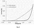
- Comparative Example 2 the same 2-terminal Si/perovskite tandem cells were employed as in Comparative Example 1, with the exception that electrically insulating material in the form of a 25 ⁇ m thick, UV-cured epoxy film was provided (cf. horizontal line of the T-shape of the photograph of Fig. 7A ).
- the electrically insulating material was deposited via screen-printing using a screen with mesh size of 380-460 tpi, at a print speed of 45 mm/s, a squeegee pressure 3 kg (45° angle) and a 0.7 mm print gap.
- a UV conveyor curer was used to expose the cell to a UV dose between 500 - 1000 mJ/cm 2 , using a UV-LED lamp at 395 nm wavelength.
- Top electrically conductive pads were provided by using a silver paste to deposit 10 ⁇ m thick fingers via screen-printing over the metal track, and by drying the paste in an infrared dryer at 170°C for 20 min.
- bottom electrically conductive pads were provided in the same manner on the bottom surface of the silicon sub-cell. Four pairs of such monolithically integrated cells were then arranged so that the lower electrically conductive bond pad of the first device contacts to the upper electrically conductive bond pad of the second device and the four pairs were then laminated individually.
- Example 1 the same 2-terminal Si/perovskite tandem cells were employed as in Comparative Example 2, with the exception that the top electrically conductive pads were provided over the electrically insulating layer (see Fig. 7B ), in line with Figures 2A and 2B .
- Comparative Example 2 and Example 1 The current-voltage characteristics of Comparative Example 2 and Example 1 are shown in Figure 8 . As may be taken from the profile of Comparative Example 2, a short circuit is observed, resulting in similar C-V characteristics as Comparative Example 1.
- Example 1 the short-circuit created during lamination under the top ribbon was successfully eliminated by providing the top electrically conductive pad over the electrically insulating layer.
Landscapes
- Physics & Mathematics (AREA)
- Electromagnetism (AREA)
- Engineering & Computer Science (AREA)
- Microelectronics & Electronic Packaging (AREA)
- General Physics & Mathematics (AREA)
- Computer Hardware Design (AREA)
- Condensed Matter Physics & Semiconductors (AREA)
- Power Engineering (AREA)
- Chemical & Material Sciences (AREA)
- Inorganic Chemistry (AREA)
- Life Sciences & Earth Sciences (AREA)
- Sustainable Development (AREA)
- Materials Engineering (AREA)
- Photovoltaic Devices (AREA)
Priority Applications (8)
| Application Number | Priority Date | Filing Date | Title |
|---|---|---|---|
| EP19185692.1A EP3764406A1 (de) | 2019-07-11 | 2019-07-11 | Mehrfachfotovoltaikvorrichtung |
| CN202080059112.8A CN114270540A (zh) | 2019-07-11 | 2020-07-10 | 多结光伏器件 |
| AU2020309773A AU2020309773A1 (en) | 2019-07-11 | 2020-07-10 | Multi-junction photovoltaic device |
| EP20739357.0A EP3997740A1 (de) | 2019-07-11 | 2020-07-10 | Fotovoltaikvorrichtung mit mehreren übergängen |
| US17/626,186 US11925038B2 (en) | 2019-07-11 | 2020-07-10 | Multi-junction photovoltaic device |
| JP2022500924A JP2022539868A (ja) | 2019-07-11 | 2020-07-10 | 多重接合光起電力デバイス |
| KR1020227004718A KR20220031709A (ko) | 2019-07-11 | 2020-07-10 | 다접합 광기전 디바이스 |
| PCT/EP2020/069477 WO2021005191A1 (en) | 2019-07-11 | 2020-07-10 | Multi-junction photovoltaic device |
Applications Claiming Priority (1)
| Application Number | Priority Date | Filing Date | Title |
|---|---|---|---|
| EP19185692.1A EP3764406A1 (de) | 2019-07-11 | 2019-07-11 | Mehrfachfotovoltaikvorrichtung |
Publications (1)
| Publication Number | Publication Date |
|---|---|
| EP3764406A1 true EP3764406A1 (de) | 2021-01-13 |
Family
ID=67253733
Family Applications (2)
| Application Number | Title | Priority Date | Filing Date |
|---|---|---|---|
| EP19185692.1A Withdrawn EP3764406A1 (de) | 2019-07-11 | 2019-07-11 | Mehrfachfotovoltaikvorrichtung |
| EP20739357.0A Pending EP3997740A1 (de) | 2019-07-11 | 2020-07-10 | Fotovoltaikvorrichtung mit mehreren übergängen |
Family Applications After (1)
| Application Number | Title | Priority Date | Filing Date |
|---|---|---|---|
| EP20739357.0A Pending EP3997740A1 (de) | 2019-07-11 | 2020-07-10 | Fotovoltaikvorrichtung mit mehreren übergängen |
Country Status (7)
| Country | Link |
|---|---|
| US (1) | US11925038B2 (de) |
| EP (2) | EP3764406A1 (de) |
| JP (1) | JP2022539868A (de) |
| KR (1) | KR20220031709A (de) |
| CN (1) | CN114270540A (de) |
| AU (1) | AU2020309773A1 (de) |
| WO (1) | WO2021005191A1 (de) |
Citations (5)
| Publication number | Priority date | Publication date | Assignee | Title |
|---|---|---|---|---|
| US4617420A (en) * | 1985-06-28 | 1986-10-14 | The Standard Oil Company | Flexible, interconnected array of amorphous semiconductor photovoltaic cells |
| WO2013171517A1 (en) | 2012-05-18 | 2013-11-21 | Isis Innovation Limited | Optoelectronic devices with organometal perovskites with mixed anions |
| WO2014045021A1 (en) | 2012-09-18 | 2014-03-27 | Isis Innovation Limited | Optoelectronic device |
| WO2016198898A1 (en) | 2015-06-12 | 2016-12-15 | Oxford Photovoltaics Limited | Multijunction photovoltaic device |
| US20180158976A1 (en) * | 2016-12-02 | 2018-06-07 | Lg Electronics Inc. | Tandem solar cell and method of manufacturing the same |
Family Cites Families (5)
| Publication number | Priority date | Publication date | Assignee | Title |
|---|---|---|---|---|
| JPH11186572A (ja) | 1997-12-22 | 1999-07-09 | Canon Inc | 光起電力素子モジュール |
| CN103109378B (zh) * | 2010-09-17 | 2016-06-01 | 陶氏环球技术有限责任公司 | 改进的光伏电池组件和方法 |
| JP6586080B2 (ja) * | 2014-03-31 | 2019-10-02 | 株式会社カネカ | 太陽電池モジュールおよびその製造方法 |
| EP3660927B1 (de) * | 2018-11-30 | 2021-11-10 | CSEM Centre Suisse D'electronique Et De Microtechnique SA | Fotovoltaisches modul |
| JP7202447B2 (ja) * | 2019-03-22 | 2023-01-11 | 株式会社カネカ | 太陽電池モジュール |
-
2019
- 2019-07-11 EP EP19185692.1A patent/EP3764406A1/de not_active Withdrawn
-
2020
- 2020-07-10 EP EP20739357.0A patent/EP3997740A1/de active Pending
- 2020-07-10 KR KR1020227004718A patent/KR20220031709A/ko unknown
- 2020-07-10 AU AU2020309773A patent/AU2020309773A1/en not_active Abandoned
- 2020-07-10 US US17/626,186 patent/US11925038B2/en active Active
- 2020-07-10 CN CN202080059112.8A patent/CN114270540A/zh active Pending
- 2020-07-10 WO PCT/EP2020/069477 patent/WO2021005191A1/en unknown
- 2020-07-10 JP JP2022500924A patent/JP2022539868A/ja active Pending
Patent Citations (5)
| Publication number | Priority date | Publication date | Assignee | Title |
|---|---|---|---|---|
| US4617420A (en) * | 1985-06-28 | 1986-10-14 | The Standard Oil Company | Flexible, interconnected array of amorphous semiconductor photovoltaic cells |
| WO2013171517A1 (en) | 2012-05-18 | 2013-11-21 | Isis Innovation Limited | Optoelectronic devices with organometal perovskites with mixed anions |
| WO2014045021A1 (en) | 2012-09-18 | 2014-03-27 | Isis Innovation Limited | Optoelectronic device |
| WO2016198898A1 (en) | 2015-06-12 | 2016-12-15 | Oxford Photovoltaics Limited | Multijunction photovoltaic device |
| US20180158976A1 (en) * | 2016-12-02 | 2018-06-07 | Lg Electronics Inc. | Tandem solar cell and method of manufacturing the same |
Non-Patent Citations (3)
| Title |
|---|
| "Photovoltaic Solar Energy - from Fundamentals to Applications", 2017, WILEY, pages: 164 |
| KOJIMA, A. ET AL., JOURNAL OF THE AMERICAN CHEMICAL SOCIETY, vol. 131, no. 17, 2009, pages 6050 - 1 |
| ZUO, C. ET AL., ADV. SCI., vol. 3, 2016, pages 1500324 |
Also Published As
| Publication number | Publication date |
|---|---|
| KR20220031709A (ko) | 2022-03-11 |
| CN114270540A (zh) | 2022-04-01 |
| US11925038B2 (en) | 2024-03-05 |
| JP2022539868A (ja) | 2022-09-13 |
| EP3997740A1 (de) | 2022-05-18 |
| WO2021005191A1 (en) | 2021-01-14 |
| US20220278290A1 (en) | 2022-09-01 |
| AU2020309773A1 (en) | 2022-01-20 |
Similar Documents
| Publication | Publication Date | Title |
|---|---|---|
| EP3270432B1 (de) | Tandemsolarzelle und tandemsolarzellenmodul damit | |
| US10741708B2 (en) | Vertically stacked photovoltaic and thermal solar cell | |
| US11417787B2 (en) | Solar cell module and method for manufacturing the same | |
| EP3754729B1 (de) | Solarzellenmodul mit perowskitsolarzelle und verfahren zu seiner herstellung | |
| US11575057B2 (en) | Solar cell and method for manufacturing the same, and solar cell panel | |
| US10529882B2 (en) | Method for manufacturing multijunction photoelectric conversion device | |
| US20220059294A1 (en) | Photovoltaic structure and method of fabrication | |
| KR102543003B1 (ko) | 태양 전지 모듈 및 그 제조 방법 | |
| US20090255585A1 (en) | Flexible photovoltaic device | |
| KR101114169B1 (ko) | 태양광 발전장치 | |
| EP3970209B1 (de) | Fotovoltaikvorrichtung | |
| US11925038B2 (en) | Multi-junction photovoltaic device | |
| WO2016152857A1 (ja) | 光電変換装置 | |
| KR20190098570A (ko) | 정렬이 우수한 태양 전지 모듈 및 그 제조 방법 | |
| CN115668515A (zh) | 太阳能电池模块 | |
| CN115413373A (zh) | 太阳能电池 | |
| WO2016171157A1 (ja) | 光電変換装置 | |
| US20100116337A1 (en) | Tandem Module Photovoltaic Devices Including An Organic Module | |
| EP3817070B1 (de) | Verfahren zur herstellung einer fotovoltaikvorrichtung | |
| JP7530648B2 (ja) | 素子の製造方法 |
Legal Events
| Date | Code | Title | Description |
|---|---|---|---|
| PUAI | Public reference made under article 153(3) epc to a published international application that has entered the european phase |
Free format text: ORIGINAL CODE: 0009012 |
|
| STAA | Information on the status of an ep patent application or granted ep patent |
Free format text: STATUS: THE APPLICATION HAS BEEN PUBLISHED |
|
| AK | Designated contracting states |
Kind code of ref document: A1 Designated state(s): AL AT BE BG CH CY CZ DE DK EE ES FI FR GB GR HR HU IE IS IT LI LT LU LV MC MK MT NL NO PL PT RO RS SE SI SK SM TR |
|
| AX | Request for extension of the european patent |
Extension state: BA ME |
|
| STAA | Information on the status of an ep patent application or granted ep patent |
Free format text: STATUS: THE APPLICATION IS DEEMED TO BE WITHDRAWN |
|
| 18D | Application deemed to be withdrawn |
Effective date: 20210714 |