EP3761506A1 - Composite substrate and piezoelectric element - Google Patents
Composite substrate and piezoelectric element Download PDFInfo
- Publication number
- EP3761506A1 EP3761506A1 EP19761155.1A EP19761155A EP3761506A1 EP 3761506 A1 EP3761506 A1 EP 3761506A1 EP 19761155 A EP19761155 A EP 19761155A EP 3761506 A1 EP3761506 A1 EP 3761506A1
- Authority
- EP
- European Patent Office
- Prior art keywords
- substrate
- hole
- piezoelectric
- composite substrate
- support substrate
- Prior art date
- Legal status (The legal status is an assumption and is not a legal conclusion. Google has not performed a legal analysis and makes no representation as to the accuracy of the status listed.)
- Pending
Links
- 239000000758 substrate Substances 0.000 title claims abstract description 121
- 239000002131 composite material Substances 0.000 title claims abstract description 35
- 239000004020 conductor Substances 0.000 claims abstract description 11
- 230000003247 decreasing effect Effects 0.000 claims abstract description 10
- 230000000149 penetrating effect Effects 0.000 claims abstract description 7
- GQYHUHYESMUTHG-UHFFFAOYSA-N lithium niobate Chemical compound [Li+].[O-][Nb](=O)=O GQYHUHYESMUTHG-UHFFFAOYSA-N 0.000 claims description 5
- 229910052594 sapphire Inorganic materials 0.000 claims description 5
- 239000010980 sapphire Substances 0.000 claims description 5
- WSMQKESQZFQMFW-UHFFFAOYSA-N 5-methyl-pyrazole-3-carboxylic acid Chemical compound CC1=CC(C(O)=O)=NN1 WSMQKESQZFQMFW-UHFFFAOYSA-N 0.000 claims description 4
- 238000010897 surface acoustic wave method Methods 0.000 claims description 3
- 230000007423 decrease Effects 0.000 claims description 2
- 238000012545 processing Methods 0.000 description 7
- 239000000463 material Substances 0.000 description 6
- 238000000034 method Methods 0.000 description 6
- 238000004519 manufacturing process Methods 0.000 description 4
- HEMHJVSKTPXQMS-UHFFFAOYSA-M Sodium hydroxide Chemical compound [OH-].[Na+] HEMHJVSKTPXQMS-UHFFFAOYSA-M 0.000 description 3
- 238000005452 bending Methods 0.000 description 3
- 238000005530 etching Methods 0.000 description 3
- 230000003746 surface roughness Effects 0.000 description 3
- KRHYYFGTRYWZRS-UHFFFAOYSA-N Fluorane Chemical compound F KRHYYFGTRYWZRS-UHFFFAOYSA-N 0.000 description 2
- VEXZGXHMUGYJMC-UHFFFAOYSA-N Hydrochloric acid Chemical compound Cl VEXZGXHMUGYJMC-UHFFFAOYSA-N 0.000 description 2
- NBIIXXVUZAFLBC-UHFFFAOYSA-N Phosphoric acid Chemical compound OP(O)(O)=O NBIIXXVUZAFLBC-UHFFFAOYSA-N 0.000 description 2
- XLOMVQKBTHCTTD-UHFFFAOYSA-N Zinc monoxide Chemical compound [Zn]=O XLOMVQKBTHCTTD-UHFFFAOYSA-N 0.000 description 2
- 239000000853 adhesive Substances 0.000 description 2
- 230000001070 adhesive effect Effects 0.000 description 2
- RYGMFSIKBFXOCR-UHFFFAOYSA-N Copper Chemical compound [Cu] RYGMFSIKBFXOCR-UHFFFAOYSA-N 0.000 description 1
- GRYLNZFGIOXLOG-UHFFFAOYSA-N Nitric acid Chemical compound O[N+]([O-])=O GRYLNZFGIOXLOG-UHFFFAOYSA-N 0.000 description 1
- XUIMIQQOPSSXEZ-UHFFFAOYSA-N Silicon Chemical compound [Si] XUIMIQQOPSSXEZ-UHFFFAOYSA-N 0.000 description 1
- 230000004913 activation Effects 0.000 description 1
- 230000002411 adverse Effects 0.000 description 1
- PNEYBMLMFCGWSK-UHFFFAOYSA-N aluminium oxide Inorganic materials [O-2].[O-2].[O-2].[Al+3].[Al+3] PNEYBMLMFCGWSK-UHFFFAOYSA-N 0.000 description 1
- 229910000147 aluminium phosphate Inorganic materials 0.000 description 1
- 230000015572 biosynthetic process Effects 0.000 description 1
- 238000005422 blasting Methods 0.000 description 1
- 229910021538 borax Inorganic materials 0.000 description 1
- 239000000919 ceramic Substances 0.000 description 1
- 238000004891 communication Methods 0.000 description 1
- 150000001875 compounds Chemical class 0.000 description 1
- 239000012141 concentrate Substances 0.000 description 1
- 229910052802 copper Inorganic materials 0.000 description 1
- 239000010949 copper Substances 0.000 description 1
- 239000013078 crystal Substances 0.000 description 1
- 230000002950 deficient Effects 0.000 description 1
- UQGFMSUEHSUPRD-UHFFFAOYSA-N disodium;3,7-dioxido-2,4,6,8,9-pentaoxa-1,3,5,7-tetraborabicyclo[3.3.1]nonane Chemical compound [Na+].[Na+].O1B([O-])OB2OB([O-])OB1O2 UQGFMSUEHSUPRD-UHFFFAOYSA-N 0.000 description 1
- 238000005553 drilling Methods 0.000 description 1
- 238000001312 dry etching Methods 0.000 description 1
- 230000000694 effects Effects 0.000 description 1
- 230000017525 heat dissipation Effects 0.000 description 1
- 238000010438 heat treatment Methods 0.000 description 1
- 238000009413 insulation Methods 0.000 description 1
- 229910017604 nitric acid Inorganic materials 0.000 description 1
- 238000000206 photolithography Methods 0.000 description 1
- 238000001020 plasma etching Methods 0.000 description 1
- 238000009832 plasma treatment Methods 0.000 description 1
- 229910052710 silicon Inorganic materials 0.000 description 1
- 239000010703 silicon Substances 0.000 description 1
- HBMJWWWQQXIZIP-UHFFFAOYSA-N silicon carbide Chemical compound [Si+]#[C-] HBMJWWWQQXIZIP-UHFFFAOYSA-N 0.000 description 1
- 229910010271 silicon carbide Inorganic materials 0.000 description 1
- 239000004328 sodium tetraborate Substances 0.000 description 1
- 235000010339 sodium tetraborate Nutrition 0.000 description 1
- 238000004544 sputter deposition Methods 0.000 description 1
- 239000000126 substance Substances 0.000 description 1
- 238000007740 vapor deposition Methods 0.000 description 1
- 238000001039 wet etching Methods 0.000 description 1
- 239000011787 zinc oxide Substances 0.000 description 1
Images
Classifications
-
- H—ELECTRICITY
- H03—ELECTRONIC CIRCUITRY
- H03H—IMPEDANCE NETWORKS, e.g. RESONANT CIRCUITS; RESONATORS
- H03H9/00—Networks comprising electromechanical or electro-acoustic elements; Electromechanical resonators
- H03H9/25—Constructional features of resonators using surface acoustic waves
-
- H—ELECTRICITY
- H03—ELECTRONIC CIRCUITRY
- H03H—IMPEDANCE NETWORKS, e.g. RESONANT CIRCUITS; RESONATORS
- H03H9/00—Networks comprising electromechanical or electro-acoustic elements; Electromechanical resonators
- H03H9/02—Details
- H03H9/02535—Details of surface acoustic wave devices
- H03H9/02543—Characteristics of substrate, e.g. cutting angles
- H03H9/02574—Characteristics of substrate, e.g. cutting angles of combined substrates, multilayered substrates, piezoelectrical layers on not-piezoelectrical substrate
-
- H—ELECTRICITY
- H03—ELECTRONIC CIRCUITRY
- H03H—IMPEDANCE NETWORKS, e.g. RESONANT CIRCUITS; RESONATORS
- H03H3/00—Apparatus or processes specially adapted for the manufacture of impedance networks, resonating circuits, resonators
- H03H3/007—Apparatus or processes specially adapted for the manufacture of impedance networks, resonating circuits, resonators for the manufacture of electromechanical resonators or networks
- H03H3/08—Apparatus or processes specially adapted for the manufacture of impedance networks, resonating circuits, resonators for the manufacture of electromechanical resonators or networks for the manufacture of resonators or networks using surface acoustic waves
-
- H—ELECTRICITY
- H03—ELECTRONIC CIRCUITRY
- H03H—IMPEDANCE NETWORKS, e.g. RESONANT CIRCUITS; RESONATORS
- H03H9/00—Networks comprising electromechanical or electro-acoustic elements; Electromechanical resonators
- H03H9/02—Details
- H03H9/02535—Details of surface acoustic wave devices
- H03H9/02543—Characteristics of substrate, e.g. cutting angles
- H03H9/02559—Characteristics of substrate, e.g. cutting angles of lithium niobate or lithium-tantalate substrates
-
- H—ELECTRICITY
- H10—SEMICONDUCTOR DEVICES; ELECTRIC SOLID-STATE DEVICES NOT OTHERWISE PROVIDED FOR
- H10N—ELECTRIC SOLID-STATE DEVICES NOT OTHERWISE PROVIDED FOR
- H10N30/00—Piezoelectric or electrostrictive devices
- H10N30/80—Constructional details
- H10N30/87—Electrodes or interconnections, e.g. leads or terminals
- H10N30/875—Further connection or lead arrangements, e.g. flexible wiring boards, terminal pins
Definitions
- the present disclosure relates to a composite substrate having a structure in which a piezoelectric substrate and a support substrate are bonded together, and a piezoelectric device with this composite substrate.
- piezoelectric devices such as surface acoustic wave devices used in communication devices such as mobile phones.
- a small and high performance piezoelectric device there is a device that supplies electrical signals to the element electrodes formed on a piezoelectric substrate through a conductor formed in a through hole penetrating a composite substrate composed of the piezoelectric substrate and a support substrate bonded together.
- Patent Document 1 suggests a composite substrate in which both substrates are bonded together and a through hole is formed.
- Patent Documents 2 and 3 suggest a composite substrate in which holes are formed in both substrates and then bonded together.
- the composite substrate of the present disclosure includes a piezoelectric substrate having a first surface and a second surface opposing the first surface, a support substrate having a third surface in contact with the second surface and a fourth surface opposing the third surface, and a through hole penetrating from the first surface to the fourth surface.
- the through hole has a tapered shape having a diameter decreasing from the first surface to the fourth surface and has a stepped surface at which a diameter decreases in the support substrate.
- the piezoelectric device of the present disclosure includes the composite substrate and a conductor located within the through hole.
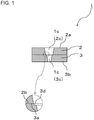
- Fig. 1 is a schematic sectional view showing an example of the composite substrate of the present disclosure.
- Fig. 1 shows a schematic sectional view of a composite substrate 1 of the present disclosure.
- the composite substrate 1 of the present disclosure has a piezoelectric substrate 2 having a first surface 2a and a second surface 2b opposing the first surface 2a, a support substrate 3 having a third surface 3a coming in contact with the second surface 2b and a fourth surface 3b opposing the third surface 3a, and a through hole 1c penetrating from the first surface 2a to the fourth surface 3b.
- the through hole 1c has a tapered shape with a diameter decreasing from the first surface 2a to the fourth surface 3b.
- the through hole 1c has a stepped surface 3d at which the diameter of the through hole 1c is decreased in the support substrate 3.
- the sectional shape perpendicular to the penetrating direction of the through hole 1c is not particularly restricted.
- the sectional shape perpendicular to the penetrating direction of the through hole 1c is, for example, circular.
- the dimensions of the composite substrate 1, for example, are 4 inches to 8 inches in diameter, the thickness of the support substrate 3 is 0.08 mm to 1.5 mm, and the thickness of the piezoelectric substrate 2 is 0.1 ⁇ m to 50 ⁇ m.
- the composite substrate 1 of the present disclosure is used as a composite substrate 1 for piezoelectric devices such as surface acoustic wave devices.
- a plurality of piezoelectric devices is formed on a single composite substrate 1.
- An element electrode is formed on the first surface 2a of the piezoelectric substrate 2.
- An external electrode is formed on the fourth surface 3b of the support substrate 3.
- a conductor made of a conductive material such as copper is formed inside the through hole 1c. This conductor is connected to the element electrode on the first surface 2a and the external electrode on the fourth surface 3b.
- the conductor is formed inside the through hole 1c by vapor deposition, sputtering, or other methods.
- the composite substrate 1 and the piezoelectric device of the present disclosure have the through hole 1c.
- the through hole 1c has a tapered shape with a diameter decreasing from the first surface 2a to the fourth surface 3b and has a stepped surface 3d with a diameter decreasing in the support substrate 3.
- the composite substrate 1 and the piezoelectric device of the present disclosure have high adhesion between the inner surface of the through hole 1c and the conductor.
- the conductor located on the stepped surface 3d has a part which is bended (bending part), it is not located on the sticking surface of the second surface 2b and the third surface 3a. Therefore, it is less likely to occur a detachment of the sticking surface between the second surface 2b and the third surface 3a.
- the composite substrate 1 and the piezoelectric device of the present disclosure have excellent reliability and can be used for a long period of time.
- an arithmetic mean roughness Ra of the stepped surface 3d and the region on the first surface 2a side from the stepped surface 3d may be smaller than an arithmetic mean roughness Ra of the region on the fourth surface 3b side from the stepped surface 3d.
- the piezoelectric substrate 2 is less likely to be damaged, the stress concentration applied to the bending part is suppressed, and the region on the fourth surface 3b side has higher adhesion than the stepped surface 3d. Therefore, the reliability of the composite substrate 1 and the piezoelectric device is increased.
- the stepped surface 3d and the region on the first surface 2a side from the stepped surface 3d has a small arithmetic mean roughness Ra and a surface property that is difficult to concentrate stress. Therefore, the piezoelectric substrate 2 is less likely to be damaged and the stress concentration applied to the bending part is suppressed.
- the adhesion of the region on the fourth surface 3b side being higher than that of the stepped surface 3d is due to an anchor effect.
- the piezoelectric substrate 2 is composed of piezoelectric materials such as lithium tantalate (LT), lithium niobate (LN), zinc oxide, and crystal.
- the support substrate 3 is composed of a material with higher mechanical strength than the piezoelectric substrate 2.
- the support substrate 3 is configured from various ceramics, such as sapphire, silicon, silicon carbide, LN, alumina. Among them, sapphire has excellent mechanical strength, insulation, and heat dissipation properties, making it a suitable material for the support substrate 3.
- the piezoelectric substrate 2 having the first surface 2a and the second surface 2b opposing the first surface 2a, and the support substrate 3 having the third surface 3a and the fourth surface 3b opposing the third surface 3a are prepared.
- a process forming a tapered second hole 2c, which penetrates from the first surface 2a side to the second surface 2b side of the piezoelectric substrate 2 is performed.
- the hole diameter of the second hole 2c on the second surface 2b is processed so as to be larger than the hole diameter in the third surface 3a at the time of bonding, and the hole diameter on the third surface 3a side (the piezoelectric substrate 2 side of the first hole 3c) is processed so as to be larger in diameter than when it is bonded.
- the holes can be formed by laser-processing, blasting or drilling.
- sapphire is used as the support substrate 3 and the first hole 3c is formed by laser processing
- a short pulsed UV laser using harmonics such as a YAG laser is suitable.
- the support substrate 3 is laser-processed, debris scattered from the processing area during processing adheres to the surface and processed surface of the support substrate 3. Debris will adversely affect subsequent manufacturing processes and product characteristics. Therefore, debris is removed by etching or other methods.
- etching with hydrochloric acid, nitric acid, hydrofluoric acid, phosphoric acid, sodium tetraborate melt, KOH melt, and NaOH melt can be used.
- the piezoelectric substrate 2 and the support substrate 3 are bonded together by direct bonding without using an adhesive material, or by bonding with an adhesive material.
- direct bonding the piezoelectric substrate 2 and the support substrate 3 are joined by heating and/or pressurizing them in vacuum, in air or in a predetermined atmosphere. Stresses are generated in the piezoelectric substrate 2 and the support substrate 3 due to the temperature at the time of bonding and the difference in the thermal expansion rate between the piezoelectric substrate 2 and the support substrate 3, which may cause damage and defective processing accuracy. In order to reduce such stresses, it is preferable that a bonding temperature is low.
- the second surface 2b of the piezoelectric substrate 2 and the third surface 3a of the support substrate 3 may be joined after activation treatment is applied by a method such as plasma treatment.
- the second hole 2c is formed.
- the second hole 2c may be formed after grinding the first surface 2a of the piezoelectric substrate 2 using a lapping device or the like to reduce the thickness of the piezoelectric substrate 2.
- piezoelectric materials have low mechanical strength. Therefore, it is preferred to form the second hole 2c on the piezoelectric substrate 2 by chemical treatment such as wet etching and dry etching. If the piezoelectric substrate 2 is made of LT or LN, it can be formed by a combination of mask formation by photolithography technique and reactive ion etching using a halogenated compound gas such as CF 4 .
- an etched surface has a smaller surface roughness than a laser processed surface.
- the surface roughness can be expressed, for example, as the arithmetic mean roughness Ra.
- the surface roughness of the stepped surface 3d and the region on the first surface 2a side (piezoelectric substrate 2 side) from the stepped surface 3d can be smaller than that of the region on the fourth surface 3b side (support substrate 3 side) from the stepped surface 3d.
- a tapered through hole decreasing diameter from one surface of the substrate (a first surface of the piezoelectric substrate) to the other surface (a fourth surface of the support substrate) has a stepped surface decreasing diameter in the support substrate.
- the piezoelectric substrate 2 and the support substrate 3 are first bonded together, and then a through hole having a small diameter is formed. After that, a through hole 3c is formed by processing to widen the diameter of the small through hole on the piezoelectric substrate 2 side in the piezoelectric substrate 2 and the support substrate 3.
- the second hole 2c having a tapered shape is first formed in the piezoelectric substrate 2, and the first hole 3c having an overall tapered shape and a stepped part 3d is formed in the support substrate 3. Then, by bonding the piezoelectric substrate 2 and the support substrate 3 together, the through hole 3c in which the second hole 2c and the first hole 3c are connected may be formed.
Landscapes
- Physics & Mathematics (AREA)
- Acoustics & Sound (AREA)
- Engineering & Computer Science (AREA)
- Chemical & Material Sciences (AREA)
- Materials Engineering (AREA)
- Manufacturing & Machinery (AREA)
- Surface Acoustic Wave Elements And Circuit Networks Thereof (AREA)
- Piezo-Electric Or Mechanical Vibrators, Or Delay Or Filter Circuits (AREA)
- Production Of Multi-Layered Print Wiring Board (AREA)
- Printing Elements For Providing Electric Connections Between Printed Circuits (AREA)
- Structure Of Printed Boards (AREA)
Abstract
Description
- The present disclosure relates to a composite substrate having a structure in which a piezoelectric substrate and a support substrate are bonded together, and a piezoelectric device with this composite substrate.
- In recent years, there has been a demand for miniaturization and higher performance of piezoelectric devices such as surface acoustic wave devices used in communication devices such as mobile phones. As a small and high performance piezoelectric device, there is a device that supplies electrical signals to the element electrodes formed on a piezoelectric substrate through a conductor formed in a through hole penetrating a composite substrate composed of the piezoelectric substrate and a support substrate bonded together.
- As such composite substrates for piezoelectric devices,
Patent Document 1 suggests a composite substrate in which both substrates are bonded together and a through hole is formed.Patent Documents -
- Patent Document 1: Japanese Unexamined Patent Publication No.
2011-130385 - Patent Document 1: Japanese Unexamined Patent Publication No.
2003-37471 - Patent Document 1: Japanese Unexamined Patent Publication No.
2010-50539 - The composite substrate of the present disclosure includes a piezoelectric substrate having a first surface and a second surface opposing the first surface, a support substrate having a third surface in contact with the second surface and a fourth surface opposing the third surface, and a through hole penetrating from the first surface to the fourth surface. The through hole has a tapered shape having a diameter decreasing from the first surface to the fourth surface and has a stepped surface at which a diameter decreases in the support substrate. The piezoelectric device of the present disclosure includes the composite substrate and a conductor located within the through hole.
-
Fig. 1 is a schematic sectional view showing an example of the composite substrate of the present disclosure. - The composite substrate and the piezoelectric device of the present disclosure will be described with reference to the figure.
-
Fig. 1 shows a schematic sectional view of acomposite substrate 1 of the present disclosure. Thecomposite substrate 1 of the present disclosure has apiezoelectric substrate 2 having afirst surface 2a and asecond surface 2b opposing thefirst surface 2a, asupport substrate 3 having athird surface 3a coming in contact with thesecond surface 2b and afourth surface 3b opposing thethird surface 3a, and a through hole 1c penetrating from thefirst surface 2a to thefourth surface 3b. The through hole 1c has a tapered shape with a diameter decreasing from thefirst surface 2a to thefourth surface 3b. The through hole 1c has astepped surface 3d at which the diameter of the through hole 1c is decreased in thesupport substrate 3.Fig. 1 shows an example in which thestepped surface 3d is substantially parallel to thethird surface 3a. The sectional shape perpendicular to the penetrating direction of the through hole 1c is not particularly restricted. The sectional shape perpendicular to the penetrating direction of the through hole 1c is, for example, circular. The dimensions of thecomposite substrate 1, for example, are 4 inches to 8 inches in diameter, the thickness of thesupport substrate 3 is 0.08 mm to 1.5 mm, and the thickness of thepiezoelectric substrate 2 is 0.1 µm to 50 µm. - The
composite substrate 1 of the present disclosure is used as acomposite substrate 1 for piezoelectric devices such as surface acoustic wave devices. A plurality of piezoelectric devices is formed on asingle composite substrate 1. An element electrode is formed on thefirst surface 2a of thepiezoelectric substrate 2. An external electrode is formed on thefourth surface 3b of thesupport substrate 3. A conductor made of a conductive material such as copper is formed inside the through hole 1c. This conductor is connected to the element electrode on thefirst surface 2a and the external electrode on thefourth surface 3b. The conductor is formed inside the through hole 1c by vapor deposition, sputtering, or other methods. - The
composite substrate 1 and the piezoelectric device of the present disclosure have the through hole 1c. The through hole 1c has a tapered shape with a diameter decreasing from thefirst surface 2a to thefourth surface 3b and has a steppedsurface 3d with a diameter decreasing in thesupport substrate 3. Thus, thecomposite substrate 1 and the piezoelectric device of the present disclosure have high adhesion between the inner surface of the through hole 1c and the conductor. Although the conductor located on thestepped surface 3d has a part which is bended (bending part), it is not located on the sticking surface of thesecond surface 2b and thethird surface 3a. Therefore, it is less likely to occur a detachment of the sticking surface between thesecond surface 2b and thethird surface 3a. Since thestepped surface 3d is located in the supportingsubstrate 3, there is no risk of damage to the element electrodes (piezoelectric devices) of thepiezoelectric substrate 2. As a result, thecomposite substrate 1 and the piezoelectric device of the present disclosure have excellent reliability and can be used for a long period of time. - In the through hole 1c, an arithmetic mean roughness Ra of the
stepped surface 3d and the region on thefirst surface 2a side from thestepped surface 3d may be smaller than an arithmetic mean roughness Ra of the region on thefourth surface 3b side from thestepped surface 3d. - When Such a configuration is satisfied, the
piezoelectric substrate 2 is less likely to be damaged, the stress concentration applied to the bending part is suppressed, and the region on thefourth surface 3b side has higher adhesion than thestepped surface 3d. Therefore, the reliability of thecomposite substrate 1 and the piezoelectric device is increased. - In the through hole 1c, the
stepped surface 3d and the region on thefirst surface 2a side from thestepped surface 3d has a small arithmetic mean roughness Ra and a surface property that is difficult to concentrate stress. Therefore, thepiezoelectric substrate 2 is less likely to be damaged and the stress concentration applied to the bending part is suppressed. - In the through hole 1c, the adhesion of the region on the
fourth surface 3b side being higher than that of thestepped surface 3d is due to an anchor effect. - The
piezoelectric substrate 2 is composed of piezoelectric materials such as lithium tantalate (LT), lithium niobate (LN), zinc oxide, and crystal. Thesupport substrate 3 is composed of a material with higher mechanical strength than thepiezoelectric substrate 2. Thesupport substrate 3 is configured from various ceramics, such as sapphire, silicon, silicon carbide, LN, alumina. Among them, sapphire has excellent mechanical strength, insulation, and heat dissipation properties, making it a suitable material for thesupport substrate 3. - An example of a manufacturing method of the
composite substrate 1 of the present disclosure is shown below. - First, the
piezoelectric substrate 2 having thefirst surface 2a and thesecond surface 2b opposing thefirst surface 2a, and thesupport substrate 3 having thethird surface 3a and thefourth surface 3b opposing thethird surface 3a are prepared. - Next, it is processed to form a tapered
first hole 3c, which penetrates from thethird surface 3a side to thefourth surface 3b side of thesupport substrate 3. - Then, the
third surface 3a of thesupport substrate 3 in which thefirst hole 3c is formed and thesecond surface 2b of thepiezoelectric substrate 2 are bonded together. - Finally, a process forming a tapered second hole 2c, which penetrates from the
first surface 2a side to thesecond surface 2b side of thepiezoelectric substrate 2 is performed. At this time, the hole diameter of the second hole 2c on thesecond surface 2b is processed so as to be larger than the hole diameter in thethird surface 3a at the time of bonding, and the hole diameter on thethird surface 3a side (thepiezoelectric substrate 2 side of thefirst hole 3c) is processed so as to be larger in diameter than when it is bonded. - The holes can be formed by laser-processing, blasting or drilling. When sapphire is used as the
support substrate 3 and thefirst hole 3c is formed by laser processing, a short pulsed UV laser using harmonics such as a YAG laser is suitable. When thesupport substrate 3 is laser-processed, debris scattered from the processing area during processing adheres to the surface and processed surface of thesupport substrate 3. Debris will adversely affect subsequent manufacturing processes and product characteristics. Therefore, debris is removed by etching or other methods. For debris removal of thesupport substrate 3 comprising sapphire, for example, etching with hydrochloric acid, nitric acid, hydrofluoric acid, phosphoric acid, sodium tetraborate melt, KOH melt, and NaOH melt can be used. - The
piezoelectric substrate 2 and thesupport substrate 3 are bonded together by direct bonding without using an adhesive material, or by bonding with an adhesive material. In direct bonding, thepiezoelectric substrate 2 and thesupport substrate 3 are joined by heating and/or pressurizing them in vacuum, in air or in a predetermined atmosphere. Stresses are generated in thepiezoelectric substrate 2 and thesupport substrate 3 due to the temperature at the time of bonding and the difference in the thermal expansion rate between thepiezoelectric substrate 2 and thesupport substrate 3, which may cause damage and defective processing accuracy. In order to reduce such stresses, it is preferable that a bonding temperature is low. For this purpose, thesecond surface 2b of thepiezoelectric substrate 2 and thethird surface 3a of thesupport substrate 3 may be joined after activation treatment is applied by a method such as plasma treatment. - After the
piezoelectric substrate 2 and thesupport substrate 3 are bonded together, the second hole 2c is formed. The second hole 2c may be formed after grinding thefirst surface 2a of thepiezoelectric substrate 2 using a lapping device or the like to reduce the thickness of thepiezoelectric substrate 2. - In general, piezoelectric materials have low mechanical strength. Therefore, it is preferred to form the second hole 2c on the
piezoelectric substrate 2 by chemical treatment such as wet etching and dry etching. If thepiezoelectric substrate 2 is made of LT or LN, it can be formed by a combination of mask formation by photolithography technique and reactive ion etching using a halogenated compound gas such as CF4. - In general, an etched surface has a smaller surface roughness than a laser processed surface. The surface roughness can be expressed, for example, as the arithmetic mean roughness Ra. Of the through hole 1c, if the
first hole 3c is formed by laser processing and the steppedsurface 3d and the second hole 2c are formed by etching, in the through hole 1c, the surface roughness of the steppedsurface 3d and the region on thefirst surface 2a side (piezoelectric substrate 2 side) from the steppedsurface 3d can be smaller than that of the region on thefourth surface 3b side (support substrate 3 side) from the steppedsurface 3d. - In the composite substrate and the piezoelectric device of the present disclosure, a tapered through hole decreasing diameter from one surface of the substrate (a first surface of the piezoelectric substrate) to the other surface (a fourth surface of the support substrate) has a stepped surface decreasing diameter in the support substrate. As a result, adhesion between the inner surface of the through hole and the conductor is increased, and it is less likely to cause a detachment of the bonding surface of the substrate and stress concentration on the piezoelectric substrate having no stepped surface. Therefore, a composite substrate and a piezoelectric device with excellent reliability can be provided.
- The following methods are used as a manufacturing method of the
composite substrate 1. For example, thepiezoelectric substrate 2 and thesupport substrate 3 are first bonded together, and then a through hole having a small diameter is formed. After that, a throughhole 3c is formed by processing to widen the diameter of the small through hole on thepiezoelectric substrate 2 side in thepiezoelectric substrate 2 and thesupport substrate 3. - Alternatively, the second hole 2c having a tapered shape is first formed in the
piezoelectric substrate 2, and thefirst hole 3c having an overall tapered shape and a steppedpart 3d is formed in thesupport substrate 3. Then, by bonding thepiezoelectric substrate 2 and thesupport substrate 3 together, the throughhole 3c in which the second hole 2c and thefirst hole 3c are connected may be formed. - Although the embodiments of the present disclosure have been described above, the present disclosure is not limited to the above-described embodiments, and various improvements and changes may be made within the scope of the claims.
-
- 1:
- Composite Substrate
- 1c:
- Through hole
- 2:
- Piezoelectric Substrate
- 2a:
- First Surface
- 2b:
- Second Surface
- 2c:
- Second Hole
- 3:
- Support Substrate
- 3a:
- Third Surface
- 3b:
- Fourth Surface
- 3c:
- First Hole
- 3d:
- Stepped Surface
Claims (7)
- A composite substrate comprising:a piezoelectric substrate having a first surface and a second surface opposing the first surface,a support substrate having a third surface in contact with the second surface and a fourth surface opposing the third surface, anda through hole penetrating from the first surface to the fourth surface,wherein the through hole has a tapered shape having a diameter decreasing from the first surface to the fourth surface and a stepped surface at which a diameter decreases in the support substrate.
- The composite substrate according to Claim 1, wherein the piezoelectric substrate is a lithium tantalate substrate or a lithium niobate substrate.
- The composite substrate according to Claims 1 or 2, wherein the support substrate is a sapphire substrate.
- The composite substrate according to any of Claims 1 to 3, wherein in the through hole, an arithmetic mean roughness Ra of the stepped surface and the region on the first surface side from the stepped surface is smaller than an arithmetic mean roughness Ra of the region on the fourth surface side from the stepped surface.
- The composite substrate according to any of Claims 1 to 4, wherein the stepped surface is substantially parallel to the third surface.
- A piezoelectric device comprising the composite substrate according to any of Claims 1 to 5, and a conductor located within the through hole.
- The piezoelectric device according to Claim 6, which is a surface acoustic wave device.
Applications Claiming Priority (2)
| Application Number | Priority Date | Filing Date | Title |
|---|---|---|---|
| JP2018037267 | 2018-03-02 | ||
| PCT/JP2019/007206 WO2019167918A1 (en) | 2018-03-02 | 2019-02-26 | Composite substrate and piezoelectric element |
Publications (2)
| Publication Number | Publication Date |
|---|---|
| EP3761506A1 true EP3761506A1 (en) | 2021-01-06 |
| EP3761506A4 EP3761506A4 (en) | 2021-12-01 |
Family
ID=67804962
Family Applications (1)
| Application Number | Title | Priority Date | Filing Date |
|---|---|---|---|
| EP19761155.1A Pending EP3761506A4 (en) | 2018-03-02 | 2019-02-26 | COMPOSITE SUBSTRATE AND PIEZOELECTRIC ELEMENT |
Country Status (6)
| Country | Link |
|---|---|
| US (1) | US20210083650A1 (en) |
| EP (1) | EP3761506A4 (en) |
| JP (1) | JP6994102B2 (en) |
| CN (1) | CN111788773B (en) |
| TW (1) | TWI682630B (en) |
| WO (1) | WO2019167918A1 (en) |
Families Citing this family (3)
| Publication number | Priority date | Publication date | Assignee | Title |
|---|---|---|---|---|
| JP6898265B2 (en) * | 2018-03-02 | 2021-07-07 | 京セラ株式会社 | Manufacturing method of composite substrate |
| JP7642971B2 (en) * | 2019-08-13 | 2025-03-11 | 太陽誘電株式会社 | Electronic device and manufacturing method thereof, filter and multiplexer |
| CN113690365B (en) * | 2021-07-23 | 2024-02-13 | 绍兴中芯集成电路制造股份有限公司 | Piezoelectric device and manufacturing method |
Family Cites Families (29)
| Publication number | Priority date | Publication date | Assignee | Title |
|---|---|---|---|---|
| JPH08186467A (en) * | 1994-12-29 | 1996-07-16 | Murata Mfg Co Ltd | Divergent oscillation type piezoelectric oscillator and its production |
| JP4059406B2 (en) * | 1997-12-09 | 2008-03-12 | 株式会社村田製作所 | Method for producing glass ceramic multilayer substrate |
| JP3709802B2 (en) * | 2001-03-28 | 2005-10-26 | 株式会社村田製作所 | Manufacturing method of multilayer ceramic substrate |
| JP3772702B2 (en) | 2001-07-23 | 2006-05-10 | 松下電器産業株式会社 | Manufacturing method of surface acoustic wave device |
| JP3922079B2 (en) * | 2002-04-19 | 2007-05-30 | 株式会社村田製作所 | Manufacturing method of multilayer ceramic substrate with cavity |
| US7578058B2 (en) * | 2005-04-19 | 2009-08-25 | Tdk Corporation | Production method of a multilayer ceramic substrate |
| JP2007318058A (en) * | 2006-04-27 | 2007-12-06 | Murata Mfg Co Ltd | Electronic component and manufacturing method thereof |
| JP2008252351A (en) * | 2007-03-29 | 2008-10-16 | Murata Mfg Co Ltd | Elastic-surface wave device and manufacturing method thereof |
| JP5180975B2 (en) * | 2008-02-18 | 2013-04-10 | セイコーインスツル株式会社 | Piezoelectric vibrator manufacturing method and piezoelectric vibrator |
| US8263878B2 (en) * | 2008-03-25 | 2012-09-11 | Ibiden Co., Ltd. | Printed wiring board |
| JP4638530B2 (en) | 2008-08-19 | 2011-02-23 | 日本電波工業株式会社 | Piezoelectric component and manufacturing method thereof |
| WO2010023733A1 (en) * | 2008-08-27 | 2010-03-04 | セイコーインスツル株式会社 | Piezoelectric vibrator, oscillator, electronic apparatus, wave clock, and method for manufacturing piezoelectric vibrator |
| JP2011019043A (en) * | 2009-07-08 | 2011-01-27 | Ngk Insulators Ltd | Composite substrate and method for manufacturing composite substrate |
| JP5476964B2 (en) * | 2009-12-09 | 2014-04-23 | セイコーエプソン株式会社 | Vibrators, oscillators, gyros and electronic equipment |
| JP5056837B2 (en) | 2009-12-21 | 2012-10-24 | 株式会社村田製作所 | Method for manufacturing piezoelectric device |
| KR101661361B1 (en) * | 2010-01-14 | 2016-09-29 | 엔지케이 인슐레이터 엘티디 | Composite substrate, and elastic surface wave filter and resonator using the same |
| JP2011223234A (en) * | 2010-04-08 | 2011-11-04 | Seiko Epson Corp | Piezoelectric vibrator, piezoelectric device, through-electrode structure, semiconductor device, and semiconductor package |
| JP5855905B2 (en) * | 2010-12-16 | 2016-02-09 | 日本特殊陶業株式会社 | Multilayer wiring board and manufacturing method thereof |
| JP6092535B2 (en) * | 2012-07-04 | 2017-03-08 | 太陽誘電株式会社 | Lamb wave device and manufacturing method thereof |
| KR20160013518A (en) * | 2013-05-21 | 2016-02-04 | 엔지케이 인슐레이터 엘티디 | Method for manufacturing piezoelectric device, piezoelectric device, and piezoelectric free-standing substrate |
| KR20150053592A (en) * | 2013-11-08 | 2015-05-18 | 삼성전기주식회사 | Electric component module and manufacturing method threrof |
| CN106464232B (en) * | 2014-06-27 | 2019-09-27 | 株式会社村田制作所 | Elastic wave device and method of making the same |
| US9397053B2 (en) * | 2014-10-15 | 2016-07-19 | Hong Kong Applied Science and Technology Research Institute Company Limited | Molded device with anti-delamination structure providing multi-layered compression forces |
| CN206878791U (en) * | 2014-12-08 | 2018-01-12 | 株式会社村田制作所 | Piezoelectric device |
| JP2016201780A (en) * | 2015-04-14 | 2016-12-01 | 太陽誘電株式会社 | Elastic wave device |
| JP2017059669A (en) * | 2015-09-16 | 2017-03-23 | 大日本印刷株式会社 | A through-hole forming substrate, a through-electrode substrate, and a substrate. |
| JP2017079439A (en) * | 2015-10-22 | 2017-04-27 | 住友金属鉱山株式会社 | Manufacturing method of composite substrate |
| JP6509147B2 (en) * | 2016-02-29 | 2019-05-08 | 太陽誘電株式会社 | Electronic device |
| JP6315716B2 (en) * | 2016-03-17 | 2018-04-25 | 太陽誘電株式会社 | Elastic wave device |
-
2019
- 2019-02-26 JP JP2020503510A patent/JP6994102B2/en active Active
- 2019-02-26 US US16/971,782 patent/US20210083650A1/en not_active Abandoned
- 2019-02-26 EP EP19761155.1A patent/EP3761506A4/en active Pending
- 2019-02-26 CN CN201980016389.XA patent/CN111788773B/en active Active
- 2019-02-26 WO PCT/JP2019/007206 patent/WO2019167918A1/en not_active Ceased
- 2019-02-27 TW TW108106803A patent/TWI682630B/en active
Also Published As
| Publication number | Publication date |
|---|---|
| WO2019167918A1 (en) | 2019-09-06 |
| JPWO2019167918A1 (en) | 2021-03-11 |
| TW201939890A (en) | 2019-10-01 |
| US20210083650A1 (en) | 2021-03-18 |
| EP3761506A4 (en) | 2021-12-01 |
| JP6994102B2 (en) | 2022-01-14 |
| CN111788773B (en) | 2024-09-10 |
| CN111788773A (en) | 2020-10-16 |
| TWI682630B (en) | 2020-01-11 |
Similar Documents
| Publication | Publication Date | Title |
|---|---|---|
| EP3138120B1 (en) | Etch back processes of bonding material for the manufacture of through-glass vias | |
| KR102658526B1 (en) | Method for manufacturing composite wafer with oxide single crystal thin film | |
| EP1993948B1 (en) | Mems device | |
| EP3761506A1 (en) | Composite substrate and piezoelectric element | |
| JP4630110B2 (en) | Manufacturing method of electronic parts | |
| US20150348814A1 (en) | Electrostatic chuck and semiconductor-liquid crystal manufacturing apparatus | |
| JP2011130385A (en) | Method of manufacturing piezoelectric device | |
| US20020115263A1 (en) | Method and related apparatus of processing a substrate | |
| US8027171B2 (en) | Feeding structure of electrostatic chuck, method for producing the same, and method for regenerating feeding structure of electrostatic chuck | |
| US20250312823A1 (en) | Transducer device and method of manufacture | |
| CN115497821A (en) | SiC cutting process based on flexible carrier plate | |
| JP2007165503A (en) | Hermetic sealing structure, piezoelectric device and manufacturing method thereof | |
| JP6898265B2 (en) | Manufacturing method of composite substrate | |
| US9147831B2 (en) | Crystal unit and method for fabricating the same | |
| JP2012195504A (en) | Thin semiconductor device manufacturing method and fragile member support medium | |
| US10693439B2 (en) | Crystal vibrator and crystal vibration device | |
| CN106560916B (en) | Method for manufacturing component chip | |
| CN111441072A (en) | Method for producing crystal grains by cutting crystal grains first and then electroplating on two sides | |
| JP3427616B2 (en) | Capacitive sensor and method of manufacturing the same | |
| CN113890501A (en) | Method for forming surface acoustic wave resonance device | |
| CN109103080A (en) | Electroded reversed table top ultra thin wafer of one kind and preparation method thereof | |
| JP4439126B2 (en) | Electrostatic adsorption device | |
| CN101203938B (en) | Chemical Method for Die Dicing | |
| KR19990064545A (en) | Process for preparing static electricity chuck of ceramic type | |
| JP2002217666A (en) | Surface acoustic wave device and method of manufacturing the same |
Legal Events
| Date | Code | Title | Description |
|---|---|---|---|
| STAA | Information on the status of an ep patent application or granted ep patent |
Free format text: STATUS: THE INTERNATIONAL PUBLICATION HAS BEEN MADE |
|
| PUAI | Public reference made under article 153(3) epc to a published international application that has entered the european phase |
Free format text: ORIGINAL CODE: 0009012 |
|
| STAA | Information on the status of an ep patent application or granted ep patent |
Free format text: STATUS: REQUEST FOR EXAMINATION WAS MADE |
|
| 17P | Request for examination filed |
Effective date: 20201002 |
|
| AK | Designated contracting states |
Kind code of ref document: A1 Designated state(s): AL AT BE BG CH CY CZ DE DK EE ES FI FR GB GR HR HU IE IS IT LI LT LU LV MC MK MT NL NO PL PT RO RS SE SI SK SM TR |
|
| AX | Request for extension of the european patent |
Extension state: BA ME |
|
| DAV | Request for validation of the european patent (deleted) | ||
| DAX | Request for extension of the european patent (deleted) | ||
| REG | Reference to a national code |
Ref country code: DE Ref legal event code: R079 Free format text: PREVIOUS MAIN CLASS: H03H0009250000 Ipc: H03H0009020000 |
|
| A4 | Supplementary search report drawn up and despatched |
Effective date: 20211102 |
|
| RIC1 | Information provided on ipc code assigned before grant |
Ipc: H01L 41/312 20130101ALI20211026BHEP Ipc: H03H 3/08 20060101ALI20211026BHEP Ipc: H03H 9/02 20060101AFI20211026BHEP |
|
| P01 | Opt-out of the competence of the unified patent court (upc) registered |
Effective date: 20230508 |
|
| STAA | Information on the status of an ep patent application or granted ep patent |
Free format text: STATUS: EXAMINATION IS IN PROGRESS |
|
| 17Q | First examination report despatched |
Effective date: 20240703 |