EP3757736B1 - Anzeigevorrichtung - Google Patents
Anzeigevorrichtung Download PDFInfo
- Publication number
- EP3757736B1 EP3757736B1 EP20179009.4A EP20179009A EP3757736B1 EP 3757736 B1 EP3757736 B1 EP 3757736B1 EP 20179009 A EP20179009 A EP 20179009A EP 3757736 B1 EP3757736 B1 EP 3757736B1
- Authority
- EP
- European Patent Office
- Prior art keywords
- electrodes
- folding
- sub
- display device
- region
- Prior art date
- Legal status (The legal status is an assumption and is not a legal conclusion. Google has not performed a legal analysis and makes no representation as to the accuracy of the status listed.)
- Active
Links
Images


Classifications
-
- G—PHYSICS
- G06—COMPUTING OR CALCULATING; COUNTING
- G06F—ELECTRIC DIGITAL DATA PROCESSING
- G06F3/00—Input arrangements for transferring data to be processed into a form capable of being handled by the computer; Output arrangements for transferring data from processing unit to output unit, e.g. interface arrangements
- G06F3/01—Input arrangements or combined input and output arrangements for interaction between user and computer
- G06F3/03—Arrangements for converting the position or the displacement of a member into a coded form
- G06F3/041—Digitisers, e.g. for touch screens or touch pads, characterised by the transducing means
- G06F3/044—Digitisers, e.g. for touch screens or touch pads, characterised by the transducing means by capacitive means
- G06F3/0445—Digitisers, e.g. for touch screens or touch pads, characterised by the transducing means by capacitive means using two or more layers of sensing electrodes, e.g. using two layers of electrodes separated by a dielectric layer
-
- G—PHYSICS
- G06—COMPUTING OR CALCULATING; COUNTING
- G06F—ELECTRIC DIGITAL DATA PROCESSING
- G06F3/00—Input arrangements for transferring data to be processed into a form capable of being handled by the computer; Output arrangements for transferring data from processing unit to output unit, e.g. interface arrangements
- G06F3/01—Input arrangements or combined input and output arrangements for interaction between user and computer
- G06F3/03—Arrangements for converting the position or the displacement of a member into a coded form
- G06F3/041—Digitisers, e.g. for touch screens or touch pads, characterised by the transducing means
- G06F3/044—Digitisers, e.g. for touch screens or touch pads, characterised by the transducing means by capacitive means
-
- G—PHYSICS
- G06—COMPUTING OR CALCULATING; COUNTING
- G06F—ELECTRIC DIGITAL DATA PROCESSING
- G06F3/00—Input arrangements for transferring data to be processed into a form capable of being handled by the computer; Output arrangements for transferring data from processing unit to output unit, e.g. interface arrangements
- G06F3/01—Input arrangements or combined input and output arrangements for interaction between user and computer
- G06F3/03—Arrangements for converting the position or the displacement of a member into a coded form
- G06F3/041—Digitisers, e.g. for touch screens or touch pads, characterised by the transducing means
- G06F3/0412—Digitisers structurally integrated in a display
-
- G—PHYSICS
- G06—COMPUTING OR CALCULATING; COUNTING
- G06F—ELECTRIC DIGITAL DATA PROCESSING
- G06F3/00—Input arrangements for transferring data to be processed into a form capable of being handled by the computer; Output arrangements for transferring data from processing unit to output unit, e.g. interface arrangements
- G06F3/01—Input arrangements or combined input and output arrangements for interaction between user and computer
- G06F3/03—Arrangements for converting the position or the displacement of a member into a coded form
- G06F3/041—Digitisers, e.g. for touch screens or touch pads, characterised by the transducing means
- G06F3/044—Digitisers, e.g. for touch screens or touch pads, characterised by the transducing means by capacitive means
- G06F3/0446—Digitisers, e.g. for touch screens or touch pads, characterised by the transducing means by capacitive means using a grid-like structure of electrodes in at least two directions, e.g. using row and column electrodes
-
- G—PHYSICS
- G09—EDUCATION; CRYPTOGRAPHY; DISPLAY; ADVERTISING; SEALS
- G09F—DISPLAYING; ADVERTISING; SIGNS; LABELS OR NAME-PLATES; SEALS
- G09F9/00—Indicating arrangements for variable information in which the information is built-up on a support by selection or combination of individual elements
- G09F9/30—Indicating arrangements for variable information in which the information is built-up on a support by selection or combination of individual elements in which the desired character or characters are formed by combining individual elements
- G09F9/301—Indicating arrangements for variable information in which the information is built-up on a support by selection or combination of individual elements in which the desired character or characters are formed by combining individual elements flexible foldable or roll-able electronic displays, e.g. thin LCD, OLED
-
- H—ELECTRICITY
- H10—SEMICONDUCTOR DEVICES; ELECTRIC SOLID-STATE DEVICES NOT OTHERWISE PROVIDED FOR
- H10K—ORGANIC ELECTRIC SOLID-STATE DEVICES
- H10K59/00—Integrated devices, or assemblies of multiple devices, comprising at least one organic light-emitting element covered by group H10K50/00
- H10K59/10—OLED displays
- H10K59/12—Active-matrix OLED [AMOLED] displays
- H10K59/121—Active-matrix OLED [AMOLED] displays characterised by the geometry or disposition of pixel elements
- H10K59/1213—Active-matrix OLED [AMOLED] displays characterised by the geometry or disposition of pixel elements the pixel elements being TFTs
-
- H—ELECTRICITY
- H10—SEMICONDUCTOR DEVICES; ELECTRIC SOLID-STATE DEVICES NOT OTHERWISE PROVIDED FOR
- H10K—ORGANIC ELECTRIC SOLID-STATE DEVICES
- H10K59/00—Integrated devices, or assemblies of multiple devices, comprising at least one organic light-emitting element covered by group H10K50/00
- H10K59/10—OLED displays
- H10K59/12—Active-matrix OLED [AMOLED] displays
- H10K59/122—Pixel-defining structures or layers, e.g. banks
-
- H—ELECTRICITY
- H10—SEMICONDUCTOR DEVICES; ELECTRIC SOLID-STATE DEVICES NOT OTHERWISE PROVIDED FOR
- H10K—ORGANIC ELECTRIC SOLID-STATE DEVICES
- H10K59/00—Integrated devices, or assemblies of multiple devices, comprising at least one organic light-emitting element covered by group H10K50/00
- H10K59/10—OLED displays
- H10K59/12—Active-matrix OLED [AMOLED] displays
- H10K59/123—Connection of the pixel electrodes to the thin film transistors [TFT]
-
- H—ELECTRICITY
- H10—SEMICONDUCTOR DEVICES; ELECTRIC SOLID-STATE DEVICES NOT OTHERWISE PROVIDED FOR
- H10K—ORGANIC ELECTRIC SOLID-STATE DEVICES
- H10K59/00—Integrated devices, or assemblies of multiple devices, comprising at least one organic light-emitting element covered by group H10K50/00
- H10K59/10—OLED displays
- H10K59/12—Active-matrix OLED [AMOLED] displays
- H10K59/131—Interconnections, e.g. wiring lines or terminals
- H10K59/1315—Interconnections, e.g. wiring lines or terminals comprising structures specially adapted for lowering the resistance
-
- H—ELECTRICITY
- H10—SEMICONDUCTOR DEVICES; ELECTRIC SOLID-STATE DEVICES NOT OTHERWISE PROVIDED FOR
- H10K—ORGANIC ELECTRIC SOLID-STATE DEVICES
- H10K59/00—Integrated devices, or assemblies of multiple devices, comprising at least one organic light-emitting element covered by group H10K50/00
- H10K59/40—OLEDs integrated with touch screens
-
- G—PHYSICS
- G06—COMPUTING OR CALCULATING; COUNTING
- G06F—ELECTRIC DIGITAL DATA PROCESSING
- G06F2203/00—Indexing scheme relating to G06F3/00 - G06F3/048
- G06F2203/041—Indexing scheme relating to G06F3/041 - G06F3/045
- G06F2203/04102—Flexible digitiser, i.e. constructional details for allowing the whole digitising part of a device to be flexed or rolled like a sheet of paper
Definitions
- Embodiments of the present disclosure relate to a display device, and in particular, to a display device configured to reduce or prevent damage to a digitizer module.
- Electronic products such as a smart phone, a digital camera, a notebook computer, a navigation system, and a smart television, have a display device for displaying an image to a user.
- the display device generates an image and provides the image to a user through a screen.
- An example of such a display device is a flexible display device that can be deformed to have a curved shape, folded, or rolled.
- the use of the flexible display device allows for improvement in portability and user convenience.
- a foldable display device which is one of the flexible display devices, can be folded about a folding axis.
- a component of the foldable display device at a folding region may be damaged by various causes when the foldable display device is folded because the folding region is changed from a flat shape to a curved shape.
- US 2016/291780 A1 relates to a flexible touch screen panel comprising a thin film substrate including a first section and a second section and first sensing electrodes disposed in the first section and the second section, the first sensing electrodes being connected to one another along a first direction.
- the first sensing electrodes include a first stack structure in the first section and a second stack structure in the second section, the second stack structure being different from the first stack structure.
- aspects of some embodiments of the inventive concept are directed to a display device configured to prevent or reduce damage to a digitizer module, which is overlapped with folding regions.
- Example embodiments of the inventive concepts will now be described more fully with reference to the accompanying drawings, in which example embodiments are shown.
- Example embodiments of the inventive concepts may, however, be embodied in many different forms and should not be construed as being limited to the embodiments set forth herein; rather, these embodiments are provided so that this disclosure will be thorough and complete, and will fully convey the concept of example embodiments to those of ordinary skill in the art.
- the thicknesses of layers and regions are exaggerated for clarity.
- Like reference numerals in the drawings denote like elements, and thus their description may be omitted.
- first, second, etc. may be used herein to describe various elements, components, regions, layers and/or sections, these elements, components, regions, layers and/or sections should not be limited by these terms. These terms are only used to distinguish one element, component, region, layer or section from another element, component, region, layer or section. Thus, a first element, component, region, layer or section discussed below could be termed a second element, component, region, layer or section without departing from the teachings of example embodiments.
- spatially relative terms such as “beneath,” “below,” “lower,” “above,” “upper” and the like, may be used herein for ease of description to describe one element or feature's relationship to another element(s) or feature(s) as illustrated in the figures. It will be understood that the spatially relative terms are intended to encompass different orientations of the device in use or operation in addition to the orientation depicted in the figures. For example, if the device in the figures is turned over, elements described as “below” or “beneath” other elements or features would then be oriented “above” the other elements or features. Thus, the exemplary term “below” can encompass both an orientation of above and below. The device may be otherwise oriented (rotated 90 degrees or at other orientations) and the spatially relative descriptors used herein interpreted accordingly.
- Example embodiments of the inventive concepts are described herein with reference to cross-sectional illustrations that are schematic illustrations of idealized embodiments (and intermediate structures) of example embodiments. As such, variations from the shapes of the illustrations as a result, for example, of manufacturing techniques and/or tolerances, are to be expected. Thus, example embodiments of the inventive concepts should not be construed as limited to the particular shapes of regions illustrated herein but are to include deviations in shapes that result, for example, from manufacturing.
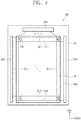
- FIG. 1 is a perspective view illustrating a display device according to some embodiments of the inventive concept.
- FIG. 2 is a perspective view illustrating a folded state of the display device of FIG. 1 .
- a display device DD may have a rectangular or tetragonal shape, whose long sides are parallel to a first direction DR1 and whose short sides are parallel to a second direction DR2 crossing the first direction DR1.
- the display device DD may have various suitable shapes including shapes that are not rectangular or tetragonal.
- a direction perpendicular to or normal to both of the first and second directions DR1 and DR2 will be referred to as a third direction DR3.
- the expression "when viewed in a plan view” may refer to a relevant structure that is seen in the third direction DR3 or a direction opposite the third direction DR3.
- "when viewed in a plan view” may refer to a top-down view, or any view from right over or a direction normal to a display surface of the display device DD.
- the display device DD may include a plurality of non-folding regions NFA1, NFA2, and NFA3 and a plurality of folding regions FA1 and FA2.
- the folding regions FA1 and FA2 may be disposed between the non-folding regions NFA1, NFA2, and NFA3, and the non-folding regions NFA1, NFA2, and NFA3 and the folding regions FA1 and FA2 may be arranged along the first direction DR1.
- the non-folding regions NFA1, NFA2, and NFA3 may include a first non-folding region NFA1, a second non-folding region NFA2, and a third non-folding region NFA3, which are sequentially arranged along the first direction DR1.
- the folding regions FA1 and FA2 may include a first folding region FA1, which is disposed between the first non-folding region NFA1 and the second non-folding region NFA2, and a second folding region FA2, which is disposed between the second non-folding region NFA2 and the third non-folding region NFA3.
- the folding regions FA1 and FA2 may be alternately arranged with the non-folding regions NFA1, NFA2, and NFA3.
- each of the folding regions FA1 and FA2 is between two non-folding regions at opposing boundaries (or edges) of the folding regions.
- the display device DD may include four or more non-folding regions and three or more folding regions.
- the number of folding regions and non-folding regions may be different.
- the number of folding regions may be less than or equal to the number of non-folding regions.
- a top surface of the display device DD may be defined as a display surface DS and may be a flat surface defined by the first direction DR1 and the second direction DR2.
- the display surface DS may include a display region DA and a non-display region NDA near or around (e.g., around the periphery of) the display region DA.
- the display region DA may be used to display an image, and the non-display region NDA may not be used to display an image.
- the non-display region NDA may enclose (e.g., encircle or surround) the display region DA and may define an edge (e.g., a periphery) of the display device DD that is printed with a set (e.g., predetermined) color.
- the display device DD may be a flexible display device.
- the display device DD may be a foldable display device that can be folded and unfolded.
- At least one of the first and second folding regions FA1 and FA2 may have a curved shape, when the display device DD is folded.
- the non-folding regions NFA1, NFA2, and NFA3 may have a substantially flat or flat shape when the display device DD is folded.
- the first folding region FA1 may be overlapped with a first folding axis FX1, and the second folding region FA2 may be overlapped with a second folding axis FX2.
- the first folding axis FX1 and the second folding axis FX2 are extended in the second direction DR2 and are spaced apart from each other along the first direction DR1.
- the first folding axis FX1 is at a center of the first folding region FA1 and the second folding axis FX2 is at a center of the second folding region FA2.
- the display device DD may be folded along (e.g., about or with respect to) the first folding axis FX1 and the second folding axis FX2. Due to this folding manner, the display device DD may be defined as a multi-folding display device (i.e., a device having more than one folding axis). In some embodiments, the display device DD may be folded in different directions on the first folding axis FX1 and the second folding axis FX2.
- the first folding region FA1 may be folded along the first folding axis FX1.
- a portion of the top surface of the display device DD e.g., a top surface of the first folding region FA1
- another portion e.g., a bottom surface of the first folding region FA1 opposite to the top surface of the first folding region FA1
- the display surface DS i.e., the top surface of the display device DD
- the display device DD may be referred to as being in an out-folding state.
- the second folding region FA2 may be folded along the second folding axis FX2.
- a portion of the top surface of the display device DD e.g., a top surface of the second folding region FA2
- another portion e.g., a bottom surface of the second folding region FA2 opposite to the top surface of the second folding region FA2
- the display device DD may be referred to as being in an in-folding state.
- first folding region FA1 may be folded to be in an out-folding state
- second folding region FA2 may be folded to be in an in-folding state
- the first non-folding region NFA1, the second non-folding region NFA2, and the third non-folding region NFA3 may be maintained to be in a substantially flat or flat state.
- both the first and second folding regions FA1 and FA2 both may be convexly curved or concavely curved with respect to the respective folding axes FX1 and FX2.
- FIG. 3 is a sectional view schematically illustrating a display module of a display device according to some embodiments of the inventive concept.
- a display module DM may include a display panel DP, a touch sensing part TSP disposed on the display panel DP, a window WIN disposed on the touch sensing part TSP, an adhesive agent OCA disposed between the touch sensing part TSP and the window WIN in the third direction DR3, and a cushion layer CSL disposed below (e.g., attached to or coupled to) the display panel DP.
- the display panel DP may be a light-emitting type display panel, but embodiments of the inventive concept are not limited to a specific type of the display panel DP.
- the display panel DP may be an organic light emitting display panel or a quantum dot light emitting display panel.
- An emission layer of the organic light emitting display panel may be formed of or include an organic luminescent material.
- An emission layer of the quantum dot light emitting display panel may include a quantum dot, a quantum rod, and/or the like.
- the description that follows will refer to an example in which the display panel DP is an organic light emitting display panel.
- the display panel DP may include a substrate SUB, a pixel layer PXL disposed on the substrate SUB, a thin encapsulation layer TFE disposed on the substrate SUB to cover the pixel layer PXL, and a protection substrate PS disposed below (e.g., attached to or coupled to) the substrate SUB.
- the substrate SUB may be a transparent substrate and may include a flexible plastic substrate.
- the substrate SUB may include polyimide (PI).
- the substrate SUB may include the display region DA and the non-display region NDA near the display region DA, similar to the display surface DS of the display device DD.
- the pixel layer PXL may be disposed on the display region DA of the substrate SUB.
- the pixel layer PXL may include a plurality of pixels, each of which includes an emission element.
- the thin encapsulation layer TFE may include at least two inorganic layers and an organic layer disposed between the inorganic layers.
- the inorganic layers may include an inorganic material and may protect the pixel layer PXL from moisture or oxygen.
- the organic layer may include an organic material and may protect the pixel layer PXL from a contamination material such as dust particles.
- the protection substrate PS may protect a bottom portion of the substrate SUB.
- the protection substrate PS may include a flexible plastic substrate.
- the protection substrate PS may include polyethylene terephthalate (PET), or any other suitable material known to those skilled in the art.
- the touch sensing part TSP may sense an external input (e.g., a touch event from a user), may generate an input signal from the sensed external input, and may provide the input signal to the display panel DP.
- the touch sensing part TSP may include a plurality of touch sensor units, which are used to sense the external input.
- the touch sensor units may sense an external input in a capacitive manner.
- the display panel DP may receive the input signal from the touch sensing part TSP and may generate an image corresponding to the input signal.
- the window WIN may protect the display panel DP and the touch sensing part TSP from an external scratch and/or an external impact.
- the window WIN may be attached to the touch sensing part TSP by the adhesive agent OCA.
- the adhesive agent OCA may include an optically clear adhesive.
- An image produced by the display panel DP may be provided to a user through the window WIN.
- the cushion layer CSL may absorb an external impact, which is exerted on a lower portion of the display module DM, thereby protecting the display panel DP.
- the cushion layer CSL may include a foam sheet having an elastic property.
- FIG. 4 is a plan view illustrating the display module of FIG. 3 .
- the display module DM may include the display panel DP, a scan driver SDV, a data driver DDV, and an emission driver EDV.
- a planar structure of the display panel DP is exemplarily illustrated in FIG. 4 , but a planar structure of the touch sensing part TSP is not shown.
- the display panel DP may be a flexible display panel.
- the display panel DP may include a plurality of electronic devices disposed on a flexible substrate.
- the display panel DP may have a rectangular shape, whose long sides are parallel to the first direction DR1 and whose short sides are parallel to the second direction DR2.
- the display panel DP may include a display region DA and a non-display region NDA enclosing (e.g., surrounding, encircling or around the periphery of) the display region DA, similar to the display surface DS of the display device DD.
- the display panel DP may include a plurality of pixels PX, a plurality of scan lines SL1-SLm, a plurality of data lines DL1-DLn, and a plurality of emission lines EL1-ELm, where m and n are natural numbers.
- the pixels PX may be arranged in a matrix shape, but embodiments of the inventive concept are not limited to this example. For example, the arrangement of the pixels PX may be variously changed in any suitable manner.
- the pixels PX may be disposed in the display region DA and may be connected to the scan lines SL1-SLm, the data lines DL1-DLn, and the emission lines EL1-ELm.
- the scan driver SDV, the data driver DDV, and the emission driver EDV may be disposed in the non-display region NDA.
- the scan driver SDV and the emission driver EDV may be disposed adjacent to the long sides, respectively, of the display panel DP.
- the data driver DDV may be manufactured in the form of an integrated circuit chip and may be disposed adjacent to one of the short sides of the display panel DP.
- the scan lines SL1-SLm may be extended in the second direction DR2 and may be connected to the scan driver SDV.
- the data lines DL1-DLn may be extended in the first direction DR1 and may be connected to the data driver DDV.
- the emission lines EL1-ELm may be extended in the second direction DR2 and may be connected to the emission driver EDV.
- the scan driver SDV may produce (or generate) a plurality of scan signals, and the scan signals may be applied to the pixels PX through the scan lines SL1-SLm.
- the scan signals may be sequentially applied to the pixels PX.
- the data driver DDV may produce (or generate) a plurality of data voltages, and the data voltages may be applied to the pixels PX through the data lines DL1-DLn.
- the emission driver EDV may produce (or generate) a plurality of emission signals, and the emission signals may be applied to the pixels PX through the emission lines EL1-ELm.
- the display module DM may include a timing controller for controlling operations of the scan driver SDV, the data driver DDV, and the emission driver EDV.
- the timing controller may generate scan control signals, data control signals, and emission control signals in response to control signals to be transmitted from the outside.
- the timing controller may receive image signals from the outside, may convert the image signals to a data format, which is suitable for interface specifications for the data driver DDV, and may provide the converted data to the data driver DDV.
- the scan driver SDV may produce (or generate) scan signals in response to the scan control signal
- the emission driver EDV may produce (or generate) emission signals in response to the emission control signal.
- the data driver DDV may receive the image signals of the converted data format and then may generate data voltages corresponding to the image signals, in response to the data control signal.
- the pixels PX may receive the data voltages in response to the scan signals.
- the pixels PX may emit light, which has a brightness level corresponding to the data voltage and constitutes an image, in response to the emission signals.
- a light-emitting time period of the pixel PX may be controlled by the emission signals.
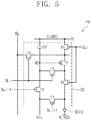
- FIG. 5 is an equivalent circuit diagram exemplarily illustrating one of pixels of FIG. 4 .
- the pixel PX may include an emission element OLED and a pixel circuit CC.
- the pixel circuit CC may include a plurality of transistors T1-T7 and a capacitor CP.
- the pixel circuit CC may control an amount of current flowing through the emission element OLED, in response to the data signal.
- the emission element OLED may emit light, whose brightness is determined by an amount of current supplied from the pixel circuit CC.
- a first voltage ELVDD may be set to a level that is higher than a level of a second voltage ELVSS.
- Each of the transistors T1-T7 may include an input or source electrode, an output or drain electrode, and a control or gate electrode.
- a first electrode one of the input and output electrodes
- a second electrode one of the input and output electrodes
- the first and second electrodes of the third transistor T3 may be disposed between and respectively coupled to the second and control electrodes of the first transistor T1.
- the control electrode of the third transistor T3 may be coupled to the i-th scan line SLi.
- the third transistor T3 may be turned on by the i-th scan signal Si, which is provided through the i-th scan line SLi to electrically connect the second and control electrodes of the first transistor T1 to each other. If the third transistor T3 is turned on, the first transistor T1 may function as a diode.
- the first and second electrodes of the fourth transistor T4 may be disposed between and respectively coupled to a node ND and an initialization power generator (e.g., a power source for providing the initialization voltage Vint).
- the control electrode of the fourth transistor T4 may be coupled to an (i-1)-th scan line SLi-1.
- the fourth transistor T4 may be turned on by an (i-1)-th scan signal Si-1 provided through the (i-1)-th scan line SLi-1 to provide the initialization voltage Vint to the node ND.
- the first and second electrodes of the fifth transistor T5 may be disposed between and respectively coupled to a power line PL and the first electrode of the first transistor T1.
- the control electrode of the fifth transistor T5 may be coupled to an i-th emission line ELi.
- the first and second electrodes of the sixth transistor T6 may be disposed between and respectively coupled to the second electrode of the first transistor T1 and the anode of the emission element OLED.
- the control electrode of the sixth transistor T6 may be coupled to the i-th emission line ELi.
- the first and second electrodes of the seventh transistor T7 may be disposed between and respectively coupled to the initialization power generator (i.e., the power source for providing the initialization voltage Vint) and the anode of the emission element OLED.
- the control electrode of the seventh transistor T7 may be coupled to an (i+1)-th scan line SLi+1.
- the seventh transistor T7 may be turned on by an (i+1)-th scan signal Si+1 provided through the (i+1)-th scan line SLi+1 to provide the initialization voltage Vint to the anode of the emission element OLED.
- FIG. 5 illustrates an example in which PMOS transistors are used as the transistors T1-T7, but embodiments of the inventive concept are not limited to this example.
- the transistors T1-T7 may be NMOS transistors, and those skilled in the art would appreciate relevant changes to the applied voltage levels and/or circuit configuration required.
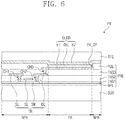
- FIG. 6 is a sectional view illustrating a portion of a display device, in which an emission element of FIG. 5 is disposed.
- the pixel PX may include the emission element OLED and a transistor TR connected to the emission element OLED.
- the emission element OLED may include a first electrode E1, a second electrode E2, and an organic emission layer OEL, which is disposed between the first electrode E1 and the second electrode E2 along the third direction DR3.
- the transistor TR may be the sixth transistor T6 shown in FIG. 5 , for example.
- the emission element OLED may be defined as an organic light emitting element.
- the first electrode E1 may be an anode, and the second electrode E2 may be a cathode.
- the first electrode E1 may be defined as a pixel electrode, and the second electrode E2 may be defined as a common electrode.
- the transistor TR and the emission element OLED may be disposed on the substrate SUB.
- a buffer layer BFL may be disposed on the substrate SUB, and in some embodiments, the buffer layer BFL may be formed of or include at least one of inorganic materials.
- a semiconductor layer SM of the transistor TR may be disposed on the buffer layer BFL.
- the semiconductor layer SM may be formed of or include at least one of suitable inorganic semiconductor materials, such as, for example, amorphous or polycrystalline silicon, or suitable organic semiconductor materials.
- the semiconductor layer SM may be formed of or include at least one of suitable oxide semiconductor materials.
- the semiconductor layer SM may include a source region, a drain region, and a channel region between the source region and the drain region.
- a first insulating layer INS1 may be disposed on the buffer layer BFL to cover the semiconductor layer SM.
- the first insulating layer INS1 may be formed of or include an inorganic material.
- a gate electrode GE of the transistor TR may be disposed on the first insulating layer INS1 and may be overlapped with the semiconductor layer SM.
- the gate electrode GE may be disposed to be overlapped with the channel region of the semiconductor layer SM.
- a second insulating layer INS2 may be disposed on the first insulating layer INS1 to cover the gate electrode GE.
- the second insulating layer INS2 may include an organic material and/or an inorganic material.
- a third insulating layer INS3 may be disposed on the second insulating layer INS2 to cover the source electrode SE and the drain electrode DE of the transistor TR.
- the third insulating layer INS3 may be defined as a planarization layer providing a substantially flat or flat top surface and may include an organic material.
- the first electrode E1 may be disposed on the third insulating layer INS3.
- the first electrode E1 may be connected to the drain electrode DE of the transistor TR through third contact holes CH3 defined in the third insulating layer INS3.
- a pixel definition layer PDL may be disposed on the first electrode E1 and the third insulating layer INS3 to expose a specific portion of the first electrode E1.
- An opening PX_OP, which exposes the specific portion of the first electrode E1, may be defined in the pixel definition layer PDL.
- the second electrode E2 may be disposed on the pixel definition layer PDL and the organic emission layer OEL.
- the thin encapsulation layer TFE may be disposed on the emission element OLED to cover the pixel PX.
- a layer between the substrate SUB and the thin encapsulation layer TFE may be defined as the pixel layer PXL.
- the first voltage ELVDD may be applied to the first electrode E1
- the second voltage ELVSS may be applied to the second electrode E2.
- the holes and electrons may be recombined to each other to produce excitons, and light may be emitted from the emission element OLED when the excitons transition to a ground state.
- the emission element OLED may emit red, green, or blue light, which constitutes a part of an image provided to a user, using a current flowing therethrough.
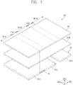
- FIG. 7 is an exploded perspective view illustrating a display device according to some embodiments of the inventive concept.
- the display device DD includes the display module DM, a digitizer module DTM disposed below (e.g., attached to or coupled to) the display module DM, and may include a supporting portion SP disposed below (e.g., attached to or coupled to) the digitizer module DTM.
- the display module DM may include first, second, and third non-folding regions NFA1, NFA2, and NFA3 and first and second folding regions FA1 and FA2, like (e.g., similar to or substantially the same as) the display device DD.
- the first, second, and third non-folding regions NFA1, NFA2, and NFA3 and the first and second folding regions FA1 and FA2 may be provided to have the same arrangement as that in the previous embodiment of FIGS. 1 and 2 , and thus, a detailed description thereof may be omitted (e.g., not repeated).
- the digitizer module DTM may have a rectangular shape, whose long sides are parallel to the first direction DR1, whose short sides are parallel to the second direction DR2.
- the digitizer module DTM may be realized in a pressure sensing manner.
- the digitizer module DTM may be configured to sense a pressure applied to the display device DD.
- the digitizer module DTM may sense a change in pressure caused by the digitizer pen.
- the digitizer module DTM may realize an input, which is associated with the sensed pressure.
- the display device DD may realize an output corresponding to the input. For example, a user may make a drawing on the display device DD using the digitizer pen.
- the supporting portion SP may support the display module DM and the digitizer module DTM.
- the supporting portion SP may include a first supporting portion SP1, a second supporting portion SP2, a third supporting portion SP3, and a plurality of joint units JU.
- the first supporting portion SP1, the second supporting portion SP2, and the third supporting portion SP3 may be arranged along the first direction DR1.
- the joint units JU may be disposed between the first supporting portion SP1 and the second supporting portion SP2 along the first direction DR1.
- the first supporting portion SP1 may be disposed below (e.g., attached to or coupled to) the digitizer module DTM and may be overlapped with the first non-folding region NFA1 when viewed from a plan view.
- the second supporting portion SP2 may be disposed below (e.g., attached to or coupled to) the digitizer module DTM and may be overlapped with the second non-folding region NFA2 when viewed from a plan view.
- the joint units JU may be disposed below (e.g., attached to or coupled to) the digitizer module DTM and may be overlapped with the first folding region FA1 when viewed from a plan view.
- the joint units JU may be extended in the second direction DR2 and may be arranged along the first direction DR1.
- the third supporting portion SP3 may be disposed below (e.g., attached to or coupled to) the digitizer module DTM and may be overlapped with the third non-folding region NFA3 when viewed from a plan view.
- the third supporting portion SP3 may be spaced apart from the second supporting portion SP2 along the first direction DR1.
- the supporting portion SP may not be disposed in a region overlapped with the second folding region FA2 when viewed from a plan view.
- the third supporting portion SP3 and the second supporting portion SP2 define opposite sides of an opening or gap in the supporting portion SP that is overlapped with the second folding region FA2 when viewed from a plan view.
- adhesive agents may be disposed between the display module DM and the digitizer module DTM and between the digitizer module DTM and the supporting portion SP.
- the display module DM, the digitizer module DTM, and the supporting portion SP may be coupled to each other by the adhesive agents.
- the adhesive agents may be pressure sensitive adhesive agents, for example.
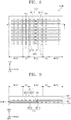
- FIG. 8 is a plan view illustrating a digitizer module of FIG. 7 .
- FIG. 9 is a sectional view taken along the line I-I' of FIG. 8 .
- the digitizer module DTM includes a plurality of first electrodes ET1 and a plurality of second electrodes ET2, which are insulated from each other and are disposed to cross each other.
- the plurality of first electrodes ET1 and the plurality of second electrodes ET2 do not intersect or physically contact each other.
- the first electrodes ET1 may be extended in the first direction DR1 and may be arranged along the second direction DR2.
- the first electrodes ET1 may be extended to cross the first and second folding axes FX1 and FX2.
- the second electrodes ET2 may be extended in the second direction DR2 and may be arranged along the first direction DR1.
- the first electrodes ET1 may be disposed below (e.g., attached to or coupled to) the second electrodes ET2. In the second folding region FA2, the first electrodes ET1 may be disposed on the second electrodes ET2.
- the first electrodes ET1 include a plurality of first sub-electrodes SET1 and a plurality of second sub-electrodes SET2.
- the first sub-electrodes SET1 are overlapped with the first folding axis FX1.
- the first sub-electrodes SET1 may be disposed to be overlapped with the first non-folding region NFA1, the first folding region FA1, and the second non-folding region NFA2.
- the second sub-electrodes SET2 are overlapped with the second folding axis FX2.
- the second sub-electrodes SET2 may be disposed to be overlapped with the third non-folding region NFA3, the second folding region FA2, and the second non-folding region NFA2.
- the first sub-electrodes SET1 and the second sub-electrodes SET2 are at different layers from each other. In the second non-folding region NFA2, the first sub-electrodes SET1 and the second sub-electrodes SET2, which are disposed at different layers, may be electrically connected to each other. Portions of the first sub-electrodes SET1 may be electrically connected to portions of the second sub-electrodes SET2 through via holes VH.
- the via holes VH according to some embodiments may be described in more detail with reference to FIG. 9 .
- the second electrodes ET2 may include a plurality of third sub-electrodes SET3 and a plurality of fourth sub-electrodes SET4.
- the third sub-electrodes SET3 may be disposed to be overlapped with the first non-folding region NFA1, the first folding region FA1, and the second non-folding region NFA2.
- the fourth sub-electrodes SET4 may be disposed to be overlapped with the third non-folding region NFA3, the second folding region FA2, and the second non-folding region NFA2.
- the third sub-electrodes SET3 may be disposed on a layer different from that below the fourth sub-electrodes SET4.
- the third sub-electrodes SET3 may be at a layer above the fourth sub-electrodes SET4.
- the fourth sub-electrodes SET4 may be at a layer below the third sub-electrodes SET3.
- the third sub-electrodes SET3 may be overlapped with the first sub-electrodes SET1, and the fourth sub-electrodes SET4 may be overlapped with the second sub-electrodes SET2.
- the first sub-electrodes SET1 may be disposed below (e.g., attached to or coupled to) the third sub-electrodes SET3, and the second sub-electrodes SET2 may be disposed on the fourth sub-electrodes SET4.
- the digitizer module DTM may include a base substrate BS, a plurality of the first electrodes ET1, a plurality of the second electrodes ET2, a first insulating layer IS1, and a second insulating layer IS2.
- the base substrate BS may include a flexible plastic substrate.
- the base substrate BS may include polyimide (PI).
- the first sub-electrodes SET1 may be disposed below (e.g., attached to or coupled to) the base substrate BS, and the second sub-electrodes SET2 may be disposed on the base substrate BS.
- the third sub-electrodes SET3 may be disposed on the base substrate BS, and the fourth sub-electrodes SET4 may be disposed below (e.g., attached to or coupled to) the base substrate BS.
- the first sub-electrodes SET1 may be disposed at a level (or layer) lower than the second sub-electrodes SET2, and the third sub-electrodes SET3 may be disposed at a level (or layer) higher than the fourth sub-electrodes SET4.
- the second sub-electrodes SET2 and the third sub-electrodes SET3 may be closer to the display module DM than the first sub-electrodes SET1 and the fourth sub-electrodes SET4 are to the display module DM.
- the second sub-electrodes SET2 may be electrically connected to the first sub-electrodes SET1 through the via holes VH, which are defined in the base substrate BS and are overlapped with the second non-folding region NFA2. Portions of the second sub-electrodes SET2 may be respectively connected to portions of the first sub-electrodes SET1 through the via holes VH.
- the first insulating layer IS1 may be disposed below (e.g., attached to or coupled to) the base substrate BS to cover the first and fourth sub-electrodes SET1 and SET4.
- the second insulating layer IS2 may be disposed on the base substrate BS to cover the second and third sub-electrodes SET2 and SET3.
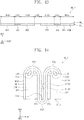
- FIG. 10 is a side view illustrating the display device of FIG. 7 according to some embodiments.
- FIG. 11 is a diagram illustrating a folded state of the display device of FIG. 10 .
- FIG. 10 illustrates a shape, viewed in the second direction DR2, of the display device DD, in which the display module DM, the digitizer module DTM, and the supporting portion SP are coupled to each other.
- An enlarged structure of the display device DD in a folded state is illustrated in FIG. 11 so as to more clearly illustrate the folded structure of the display device DD.
- the first, second, and third supporting portions SP1, SP2, and SP3 may be overlapped with the first, second, and third non-folding regions NFA1, NFA2, and NFA3, respectively, and the joint units JU may be overlapped with the first folding region FA1.
- an opening or gap in the supporting portion SP defined by the second and third support portions SP2 and SP3 may be overlapped with the second folding region FA2.
- a width of each of the joint units JU may decrease (e.g., linearly decrease) in a direction (e.g., a direction opposite the third direction DR3) from a top of each of the joint units JU toward a bottom of each of the joint units JU when viewed in the second direction DR2 (e.g., see FIG. 10 ).
- a direction opposite the third direction DR3 e.g., a direction opposite the third direction DR3
- each of the joint units JU may have an inverted trapezoidal shape.
- the first folding region FA1 and the second folding region FA2 of the display module DM may be overlapped with the first folding axis FX1 and the second folding axis FX2, respectively.
- the first folding region FA1 may be folded along the first folding axis FX1
- the second folding region FA2 may be folded along the second folding axis FX2.
- a top surface of the display module DM may be defined as the display surface DS of the display device DD.
- a bottom surface of the display module DM may be a surface, which is opposite to the top surface of the display module DM, and may be defined as a surface facing the digitizer module DTM.
- the top surface of the first folding region FA1 which is a portion of the top surface of the display module DM, may be convexly curved, and the bottom surface of the first folding region FA1 may be concavely curved.
- the first folding region FA1 may be folded in an out-folding manner.
- the first supporting portion SP1 and the second supporting portion SP2 may be disposed to face each other.
- the first non-folding region NFA1 and the second non-folding region NFA2 may be disposed at opposite sides such that they do not face each other.
- Side surfaces of the joint units JU may be disposed adjacent to each other. In some embodiments, the side surfaces of adjacent joint units JU may contact (e.g., directly contact) each other when the display device DD is folded (e.g., see FIG. 11 ).
- the top surface of the second folding region FA2 which is a portion of the top surface of the display module DM, may be concavely curved, and the bottom surface of the second folding region FA2 may be convexly curved.
- the second folding region FA2 may be folded in an in-folding manner.
- the third supporting portion SP3 may be disposed not to face (e.g., to face away from) the second supporting portion SP2.
- the second supporting portion SP2 and the third supporting portion SP3 may be disposed at opposite sides with the display module DM and the digitizer module DTM interposed therebetween.
- the second non-folding region NFA2 and the third non-folding region NFA3 may be disposed to face each other.
- the display device DD may further include a hinge structure, which is connected to the supporting portion SP to provide the first and second folding axes FX1 and FX2 to the display device DD.
- FIG. 12 is a sectional view illustrating a digitizer module of FIG. 11 .
- FIG. 12 substantially illustrates a vertical section of the digitizer module DTM of FIG. 9 , which is folded in the same manner as the display device DD of FIG. 11 .
- An enlarged structure of the digitizer module DTM in a folded state is illustrated in FIG. 12 so as to more clearly illustrate the folded structure of the digitizer module DTM according to some embodiments.
- the sectional structure of the digitizer module DTM of FIG. 12 may be described with reference to the planar structure of the digitizer module DTM of FIG. 8 .
- the second electrodes ET2 are extended parallel to first and second folding axes FX1 and FX2, the second electrodes ET2 may not be damaged, when the first and second folding regions FA1 and FA2 are folded along the first and second folding axes FX1 and FX2.
- the first electrodes ET1 are extended in a direction crossing the first and second folding axes FX1 and FX2, the first electrodes ET1 may be damaged, when the first and second folding regions FA1 and FA2 are folded along the first and second folding axes FX1 and FX2.
- a length of the top surface of the base substrate BS which is deformed to have a convexly curved shape, may become longer than a length of the bottom surface of the base substrate BS, which is deformed to have a concavely curved shape, in the first folding region FA1.
- the length of the top surface of the base substrate BS may be increased, and this may lead to an increase in strength of a tensile force exerted on the first sub-electrodes SET1.
- the first sub-electrodes SET1 may be damaged, due to such a tensile force.
- the second sub-electrodes SET2 are disposed on the top surface of the base substrate BS, which is deformed to have a concavely curved shape, and not on the bottom surface of the base substrate BS having an increasing length, it may be possible to reduce a strength of a tensile force and thereby prevent or reduce damage to the second sub-electrodes SET2.
- the display device DD may prevent or reduce damage to the digitizer module DTM, which may occur in the first and second folding regions FA1 and FA2.
- FIG. 13 is a diagram illustrating a display device according to some embodiments of the inventive concept.
- FIG. 14 is a diagram illustrating a folded state of the display device of FIG. 13 .
- FIGS. 13 and 14 substantially illustrate side views corresponding to FIGS. 10 and 11 .
- the following description may be focused on technical features of a display device DD_1 of FIGS. 13 and 14 that are different from those of the display device DD shown in FIGS. 10 and 11 , and a feature of an element previously described with reference to FIGS. 10 and 11 may be identified by the same reference number without repeating an overlapping description thereof.
- An enlarged structure of the display device DD_1 in a folded state is illustrated in FIG. 14 .
- the display device DD_1 may include a display module DM_1, a digitizer module DTM_1 disposed below (e.g., attached to or coupled to) the display module DM_1, and a supporting portion SP_1 disposed below (e.g., attached to or coupled to) a digitizer module DTM_1.
- the display module DM_1 may include first, second, third, and fourth non-folding regions NFA1, NFA2, NFA3, and NFA4 that are arranged along the first direction DR1, and first, second, and third folding regions FA1, FA2, and FA3 that are disposed between the first, second, third, and fourth non-folding regions NFA1, NFA2, NFA3, and NFA4.
- the third folding region FA3 may be disposed between the third non-folding region NFA3 and the fourth non-folding region NFA4.
- the supporting portion SP_1 may include first, second, third, and fourth supporting portions SP1, SP2, SP3, and SP4 and first and second joint units JU1 and JU2.
- the fourth supporting portion SP4 may be disposed below (e.g., attached to or coupled to) the digitizer module DTM_1 and may be overlapped with the fourth non-folding region NFA4.
- the first joint units JU1 may be substantially the same as or the same as the joint units JU shown in FIGS. 10 and 11 .
- the second joint units JU2 may be substantially the same as or the same as (e.g., may have substantially the same shape as or the same shape as) the first joint units JU1.
- the second joint units JU2 may be overlapped with the third folding region FA3 and may be disposed below (e.g., attached to or coupled to) the digitizer module DTM_1.
- the second joint units JU2 may be disposed between the third supporting portion SP3 and the fourth supporting portion SP4.
- display module DM_1 and the supporting portion SP_1 may be substantially the same as or the same as those in the display module DM and the supporting portion SP described with reference to FIGS. 9 and 10 .
- the first folding region FA1 may be folded in an out-folding manner, and the second folding region FA2 may be folded in an in-folding manner.
- the third folding region FA3 may be overlapped with a third folding axis FX3 extending in the second direction DR2 and may be folded in an out-folding manner along the third folding axis FX3.
- a top surface of the third folding region FA3 may be convexly curved, and a bottom surface of the third folding region FA3 may be concavely curved.
- Side surfaces of the second joint units JU2 may be disposed adjacent to each other.
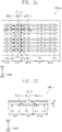
- FIG. 15 is a plan view illustrating a digitizer module of FIG. 13 .
- FIG. 16 is a diagram taken along the line II-II' of FIG. 15 .
- the digitizer module DTM_1 may include a plurality of first electrodes ET1_1, which are extended in the first direction DR1, and a plurality of second electrodes ET2, which are extended in the second direction DR2.
- the first electrodes ET1_1 may include a plurality of first sub-electrodes SET1, a plurality of second sub-electrodes SET2, and a plurality of fifth sub-electrodes SET5.
- the second electrodes ET2 are depicted with a single reference numeral, without using the terms of the sub-electrodes as in FIG. 8 .
- the second sub-electrodes SET2 may be electrically connected to the first sub-electrodes SET1 through first via holes VH1.
- the first and second sub-electrodes SET1 and SET2 may have substantially the same or the same arrangement and connection structure as those of the first and second sub-electrodes SET1 and SET2 described with reference to FIG. 8 , for example, and a detailed description thereof may be omitted (e.g., not repeated).
- the fifth sub-electrodes SET5 may be overlapped with the third folding axis FX3. In some embodiments, the fifth sub-electrodes SET5 may be overlapped with the third non-folding region NFA3, the third folding region FA3, and the fourth non-folding region NFA4. The fifth sub-electrodes SET5 and the first sub-electrodes SET1 may be disposed on the same layer or at the same level.
- the first and fifth sub-electrodes SET1 and SET5 may be disposed below (e.g., attached to or coupled to) the second electrodes ET2 in the first and third folding regions FA1 and FA3, and the second sub-electrodes SET2 may be disposed on the second electrodes ET2 in the second folding region FA2.
- the first and fifth sub-electrodes SET1 and SET5 may be disposed below (e.g., attached to or coupled to) the base substrate BS, and the second sub-electrodes SET2 may be disposed on the base substrate BS.
- the second electrodes ET2 may be disposed on the base substrate BS in the first and third folding regions FA1 and FA3 and may be disposed below (e.g., attached to or coupled to) the base substrate BS in the second folding region FA2.
- the second sub-electrodes SET2 may be electrically connected to the fifth sub-electrodes SET5 through second via holes VH2, which are defined in the base substrate BS and are overlapped with the third non-folding region NFA3.
- the fifth sub-electrodes SET5 extending across the third folding axis FX3 are disposed below (e.g., attached to or coupled to) the base substrate BS, it may be possible to prevent or to reduce damage to the fifth sub-electrodes SET5.
- FIG. 17 is a side view schematically illustrating a display device according to some embodiments of the inventive concept.
- FIG. 18 is a diagram illustrating a folded state of the display device of FIG. 17 .
- FIGS. 17 and 18 illustrate side views corresponding to FIGS. 13 and 14 .
- the following description may be focused on technical features of a display device DD_2 of FIGS. 17 and 18 that are different from those technical features of the display device DD_1 of FIGS. 13 and 14 .
- An enlarged structure of the display device DD_2 in a folded state is illustrated in FIG. 18 .
- the display device DD_2 may include a display module DM_2, a digitizer module DTM_2 disposed below (e.g., attached to or coupled to) the display module DM_2, and a supporting portion SP_2 disposed below (e.g., attached to or coupled to) the digitizer module DTM_2.
- the display module DM_2 may include the first, second, third, and fourth non-folding regions NFA1, NFA2, NFA3, and NFA4 and the first, second, and third folding regions FA1, FA2, and FA3, similar to the display module DM_1 shown in FIG. 13 .
- the display device DD_2 may be folded in an opposite manner to the display device DD_1.
- the first folding region FA1 and the third folding region FA3 may be folded in an in-folding manner along the first folding axis FX1 and the third folding axis FX3, respectively, such that the first folding region FA1 and the third folding region FA3 have concave top surfaces.
- the second folding region FA2 may be folded in an out-folding manner along the second folding axis FX2, such that the second folding region FA2 has a convex top surface.
- FIGS. 19 and 20 respectively illustrate plan and sectional views corresponding to FIGS. 15 and 16 .
- the digitizer module DTM_2 may include a plurality of first electrodes ET1_2, which are extended in the first direction DR1, and a plurality of the second electrodes ET2, which are extended in the second direction DR2.
- the first electrodes ET1_2 may include a plurality of first sub-electrodes SET1_1 , a plurality of second sub-electrodes SET2_1, and a plurality of fifth sub-electrodes SET5 1.
- the first sub-electrodes SET1_1, the second sub-electrodes SET2_1, and the fifth sub-electrodes SET5_1 may be disposed in an opposite manner to the first sub-electrodes SET1, the second sub-electrodes SET2, and the fifth sub-electrodes SET5 shown in FIGS. 15 and 16 .
- the first and fifth sub-electrodes SET1_1 and SET5_1 may be disposed on the second electrodes ET2 in the first and third folding regions FA1 and FA3, and the second sub-electrodes SET2_1 may be disposed below (e.g., attached to or coupled to) the second electrodes ET2 in the second folding region FA2.
- the first and fifth sub-electrodes SET1_1 and SET5_1 may be disposed on the base substrate BS, and the second sub-electrodes SET2_1 may be disposed below (e.g., attached to or coupled to) the base substrate BS.
- the second electrodes ET2 may be disposed below (e.g., attached to or coupled to) the base substrate BS in the first and third folding regions FA1 and FA3 and may be disposed on the base substrate BS in the second folding region FA2.
- the second sub-electrodes SET2_1 extending across the second folding axis FX2 are disposed below (e.g., attached to or coupled to) the base substrate BS, damage to the second sub-electrodes SET2_1 may be prevented or reduced.
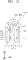
- FIG. 21 is a plan view illustrating a digitizer module according to some embodiments of the inventive concept.
- FIG. 22 is a sectional view taken along the line IV-IV' of FIG. 21 .
- FIG. 23 is a sectional view illustrating a folded state of a digitizer module of FIG. 22 .
- FIG. 21 illustrates a plan view corresponding to FIG. 8 .
- the following description may be focused on technical features of a digitizer module DTM_3 that are different from those of the digitizer module DTM of FIG. 8 .
- the digitizer module DTM_3 may include a plurality of first electrodes ET1_3, which are extended in the first direction DR1, and a plurality of second electrodes ET2, which are extended in the second direction DR2.
- the first electrodes ET1_3 may include a plurality of first sub-electrodes SET1_2, a plurality of second sub-electrodes SET2_2, and a plurality of third sub-electrodes SET3_1.
- the first sub-electrodes SET1_2 may be disposed to be overlapped with the first non-folding region NFA1.
- the second sub-electrodes SET2_2 may be disposed to be overlapped with the second and third non-folding regions NFA2 and NFA3 and the second folding region FA2.
- the second sub-electrodes SET2_2 and the first sub-electrodes SET1_2 may be disposed at (e.g., on) the same layer or at the same level.
- the third sub-electrodes SET3_1 may be overlapped with the first folding axis FX1. In some embodiments, the third sub-electrodes SET3_1 may be disposed to be overlapped with the first folding region FA1 and the first and second non-folding regions NFA1 and NFA2. The third sub-electrodes SET3_1 may be disposed between the first sub-electrodes SET1_2 and the second sub-electrodes SET2_2 in a plan view. The third sub-electrodes SET3_1 may be disposed at a level (or layer) different from that of the first sub-electrodes SET1_2 and the second sub-electrodes SET2_2.
- the first sub-electrodes SET1_2 and the second sub-electrodes SET2_2 may be disposed on the base substrate BS, and the third sub-electrodes SET3_1 may be disposed below (e.g., attached to or coupled to) the base substrate BS.
- the first sub-electrodes SET1_2 and the second sub-electrodes SET2_2 may be closer to the display module than the third sub-electrodes SET3_1 are to the display module.
- the second electrodes ET2 may be disposed on the third sub-electrodes SET3_1 in the first folding region FA1, and may be disposed below (e.g., attached to or coupled to) the first and second sub-electrodes SET1_2 and SET2_2 in the other regions NFA1, NFA2, NFA3, and FA2.
- the second electrodes ET2 may be disposed on the base substrate BS in the first folding region FA1, and may be disposed below (e.g., attached to or coupled to) the base substrate BS in the other regions NFA1, NFA2, NFA3, and FA2.
- the third sub-electrodes SET3_1 may be electrically connected to the first sub-electrodes SET1_2 through the first via holes VH1, which are defined in the base substrate BS and are overlapped with the first non-folding region NFA1.
- the third sub-electrodes SET3_1 may be electrically connected to the second sub-electrodes SET2_2 through the second via holes VH2, which are defined in the base substrate BS and are overlapped with the second non-folding region NFA2.
- a display device including the digitizer module DTM_3 may be folded in the same manner as the display device DD shown in FIG. 11 .
- the first folding region FA1 may be folded in an out-folding manner
- the second folding region FA2 may be folded in an in-folding manner.
- the third sub-electrodes SET3_1 extending across the first folding axis FX1 are disposed below (e.g., attached to or coupled to) the base substrate BS, damage to the third sub-electrodes SET3_1 may be prevented or may be reduced.
Landscapes
- Engineering & Computer Science (AREA)
- Theoretical Computer Science (AREA)
- General Engineering & Computer Science (AREA)
- Physics & Mathematics (AREA)
- General Physics & Mathematics (AREA)
- Human Computer Interaction (AREA)
- Microelectronics & Electronic Packaging (AREA)
- Geometry (AREA)
- Devices For Indicating Variable Information By Combining Individual Elements (AREA)
- Electroluminescent Light Sources (AREA)
Claims (15)
- Anzeigevorrichtung (DD), umfassend:ein Anzeigemodul (DM), das um eine erste Faltachse (FX1) und eine zweite Faltachse (FX2) faltbar ist, wobei die erste Faltachse (FX1) und die zweite Faltachse (FX2) entlang einer ersten Richtung (DR1) voneinander beabstandet sind und sich in eine zweite Richtung (DR2) erstrecken, die die erste Richtung kreuzt; undein Digitalisiermodul (DTM) unter dem Anzeigemodul (DM),wobei das Digitalisiermodul (DTM) Folgendes umfasst:eine Mehrzahl von ersten Elektroden (ET1), die sich in die erste Richtung (DR1) erstrecken und entlang der zweiten Richtung (DR2) angeordnet sind; undeine Mehrzahl von zweiten Elektroden (ET2), die sich in die zweite Richtung (DR2) erstrecken und entlang der ersten Richtung (DR1) angeordnet sind, wobei die zweiten Elektroden (ET2) von den ersten Elektroden (ET1) isoliert sind und wobei die Mehrzahl von ersten Elektroden (ET1) Folgendes umfasst:eine Mehrzahl von ersten Unterelektroden (SET1), die sich mit der ersten Faltachse (FX1) überlappen; undeine Mehrzahl von zweiten Unterelektroden (SET2), die sich mit der zweiten Faltachse (FX2) überlappen, wobei die zweiten Unterelektroden (SET2) sich auf einer anderen Schicht als die ersten Unterelektroden (SET1) befinden.
- Anzeigevorrichtung nach Anspruch 1, wobei das Digitalisiermodul dazu ausgestaltet ist, einen auf die Anzeigevorrichtung ausgeübten Druck zu erkennen.
- Anzeigevorrichtung nach Anspruch 1 oder 2, wobei die ersten Unterelektroden elektrisch mit den zweiten Unterelektroden verbunden sind.
- Anzeigevorrichtung nach einem der Ansprüche 1 bis 3, wobei das Anzeigemodul Folgendes umfasst:einen ersten, einen zweiten und einen dritten Nichtfaltbereich, die entlang der ersten Richtung angeordnet sind;einen ersten Faltbereich, der sich mit der ersten Faltachse überlappt und sich zwischen dem ersten und zweiten Nichtfaltbereich befindet; undeinen zweiten Faltbereich, der sich mit der zweiten Faltachse überlappt und sich zwischen dem zweiten und dritten Nichtfaltbereich befindet.
- Anzeigevorrichtung nach Anspruch 4, wobei die ersten Unterelektroden sich mit dem ersten Nichtfaltbereich, dem ersten Faltbereich und dem zweiten Nichtfaltbereich überlappen, unddie zweiten Unterelektroden sich mit dem dritten Nichtfaltbereich, dem zweiten Faltbereich und dem zweiten Nichtfaltbereich überlappen;wobei gegebenenfalls die Mehrzahl von zweiten Elektroden Folgendes umfasst:eine Mehrzahl von dritten Unterelektroden, die sich mit den ersten Unterelektroden überlappen; undeine Mehrzahl von vierten Unterelektroden, die sich mit den zweiten Unterelektroden überlappen, wobei die vierten Unterelektroden sich auf einer anderen Schicht als die dritten Unterelektroden befinden;wobei gegebenenfalls die ersten Unterelektroden sich unter den dritten Unterelektroden befinden und die zweiten Unterelektroden sich auf den vierten Unterelektroden befinden.
- Anzeigevorrichtung nach einem der Ansprüche 1 bis 5, wobei das Digitalisiermodul ferner ein Basissubstrat umfasst,die ersten Unterelektroden sich unter dem Basissubstrat befinden unddie zweiten Unterelektroden sich auf dem Basissubstrat befinden;wobei gegebenenfalls die zweiten Unterelektroden über Durchkontaktierungen, die in dem Basissubstrat definiert sind und sich mit dem zweiten Nichtfaltbereich überlappen, elektrisch mit den ersten Unterelektroden verbunden sind;wobei gegebenenfalls die dritten Unterelektroden sich auf dem Basissubstrat befinden und die vierten Unterelektroden sich unter dem Basissubstrat befinden.
- Anzeigevorrichtung nach einem der Ansprüche 4 bis 6, wobei der erste Faltbereich auf eine Ausfaltungsweise um die erste Faltachse faltbar ist, sodass der erste Faltbereich eine konvexe Oberseitenfläche aufweist.
- Anzeigevorrichtung nach Anspruch 7, ferner umfassend:einen ersten Tragabschnitt unter dem Digitalisiermodul und sich mit dem ersten Nichtfaltbereich überlappend;einen zweiten Tragabschnitt unter dem Digitalisiermodul und sich mit dem zweiten Nichtfaltbereich überlappend; undeine Mehrzahl von Gelenkeinheiten unter dem Digitalisiermodul und sich mit dem ersten Faltbereich überlappend,wobei die Gelenkeinheiten sich in die zweite Richtung erstrecken und entlang der ersten Richtung angeordnet sind;wobei gegebenenfalls bei einer Ansicht in die zweite Richtung eine Breite von jeder der Gelenkeinheiten sich in eine Richtung von einer Oberseite von jeder der Gelenkeinheiten zu einer Unterseite von jeder der Gelenkeinheiten hin verringert.
- Anzeigevorrichtung nach Anspruch 7 oder 8, wobei der zweite Faltbereich auf eine Einfaltungsweise um die zweite Faltachse faltbar ist, sodass der zweite Faltbereich eine konkave Oberseitenfläche aufweist;
gegebenenfalls ferner umfassend einen dritten Tragabschnitt unter dem Digitalisiermodul, der von einem zweiten Tragabschnitt beabstandet ist und sich mit dem dritten Nichtfaltbereich überlappt. - Anzeigevorrichtung nach Anspruch 4 oder 5, wobei das Anzeigemodul ferner Folgendes umfasst:einen vierten Nichtfaltbereich; undeinen dritten Faltbereich zwischen dem dritten Nichtfaltbereich und dem vierten Nichtfaltbereich, wobei der dritte Faltbereich sich mit einer dritten Faltachse überlappt, die sich in die zweite Richtung erstreckt,wobei die ersten Elektroden ferner fünfte Unterelektroden umfassen, die sich mit der dritten Faltachse überlappen, unddie fünften Unterelektroden sich auf einer gleichen Schicht wie die ersten Unterelektroden befinden.
- Anzeigevorrichtung nach Anspruch 10, wobei die ersten und fünften Unterelektroden sich in dem ersten und dritten Faltbereich unter den zweiten Elektroden befinden und
die zweiten Unterelektroden sich in dem zweiten Faltbereich auf den zweiten Elektroden befinden. - Anzeigevorrichtung nach Anspruch 11, wobei der erste und dritte Faltbereich auf eine Ausfaltungsweise entsprechend um die erste und dritte Faltachse faltbar sind, sodass der erste und dritte Faltbereich konvexe Oberseitenflächen aufweisen, und
der zweite Faltbereich auf eine Einfaltungsweise um die zweite Faltachse faltbar ist, sodass der zweite Faltbereich eine konkave Oberseitenfläche aufweist. - Anzeigevorrichtung nach Anspruch 11 oder 12, wobei das Digitalisiermodul ferner ein Basissubstrat umfasst.die ersten und fünften Unterelektroden sich unter dem Basissubstrat befinden,die zweiten Unterelektroden sich auf dem Basissubstrat befinden unddie zweiten Elektroden sich in dem ersten und dritten Faltbereich auf dem Basissubstrat befinden und sich in dem zweiten Faltbereich unter dem Basissubstrat befinden;wobei gegebenenfalls die zweiten Unterelektroden über erste Durchkontaktierungen, die in dem Basissubstrat definiert sind und sich mit dem zweiten Nichtfaltbereich überlappen, elektrisch mit den ersten Unterelektroden verbunden sind und die zweiten Unterelektroden über zweite Durchkontaktierungen, die in dem Basissubstrat definiert sind und sich mit dem dritten Nichtfaltbereich überlappen, elektrisch mit den fünften Unterelektroden verbunden sind.
- Anzeigevorrichtung nach Anspruch 10, wobei die ersten und fünften Unterelektroden sich in dem ersten und dritten Faltbereich auf den zweiten Elektroden befinden und
die zweiten Unterelektroden sich in dem zweiten Faltbereich unter den zweiten Elektroden befinden. - Anzeigevorrichtung nach Anspruch 14, wobei der erste und dritte Faltbereich auf eine Einfaltungsweise entsprechend um die erste und dritte Faltachse faltbar sind, sodass der erste und dritte Faltbereich konkave Oberseitenflächen aufweisen, und
der zweite Faltbereich auf eine Ausfaltungsweise um die zweite Faltachse faltbar ist, sodass der zweite Faltbereich eine konvexe Oberseitenfläche aufweist.
Applications Claiming Priority (1)
| Application Number | Priority Date | Filing Date | Title |
|---|---|---|---|
| KR1020190075089A KR102750020B1 (ko) | 2019-06-24 | 2019-06-24 | 표시 장치 |
Publications (2)
| Publication Number | Publication Date |
|---|---|
| EP3757736A1 EP3757736A1 (de) | 2020-12-30 |
| EP3757736B1 true EP3757736B1 (de) | 2021-09-29 |
Family
ID=71083395
Family Applications (1)
| Application Number | Title | Priority Date | Filing Date |
|---|---|---|---|
| EP20179009.4A Active EP3757736B1 (de) | 2019-06-24 | 2020-06-09 | Anzeigevorrichtung |
Country Status (4)
| Country | Link |
|---|---|
| US (2) | US11513645B2 (de) |
| EP (1) | EP3757736B1 (de) |
| KR (2) | KR102750020B1 (de) |
| CN (2) | CN112133725B (de) |
Families Citing this family (19)
| Publication number | Priority date | Publication date | Assignee | Title |
|---|---|---|---|---|
| EP4016260B1 (de) * | 2019-09-27 | 2024-04-10 | Wacom Co., Ltd. | Ortserkennungssensor und eingabevorrichtung |
| KR20210097650A (ko) * | 2020-01-30 | 2021-08-09 | 씨엠원글로벌 주식회사 | 플렉서블 디스플레이용 듀얼 디지타이저 |
| KR20220031838A (ko) * | 2020-09-04 | 2022-03-14 | 삼성디스플레이 주식회사 | 표시 장치 |
| CN114446153B (zh) * | 2020-10-30 | 2025-04-04 | 京东方科技集团股份有限公司 | 盖板及可折叠显示装置 |
| EP4216041A4 (de) | 2021-02-08 | 2024-05-29 | Samsung Electronics Co., Ltd. | Anzeigemodul zur erkennung einer stifteingabevorrichtung und elektronische vorrichtung mit dem anzeigemodul |
| KR102452863B1 (ko) * | 2021-02-25 | 2022-10-07 | 동우 화인켐 주식회사 | 디지타이저 및 이를 포함하는 화상 표시 장치 |
| KR102899549B1 (ko) | 2021-06-14 | 2025-12-15 | 삼성디스플레이 주식회사 | 표시장치 및 이를 포함하는 전자장치 |
| KR102893631B1 (ko) * | 2021-10-07 | 2025-12-02 | 삼성디스플레이 주식회사 | 전자 장치 |
| KR102940435B1 (ko) | 2021-10-26 | 2026-03-19 | 삼성디스플레이 주식회사 | 표시 장치 및 표시 장치 제조 방법 |
| KR20230106191A (ko) | 2022-01-05 | 2023-07-13 | 삼성디스플레이 주식회사 | 전자 장치 |
| KR20230116130A (ko) | 2022-01-27 | 2023-08-04 | 삼성디스플레이 주식회사 | 표시 장치 |
| KR20230116972A (ko) * | 2022-01-28 | 2023-08-07 | 삼성디스플레이 주식회사 | 폴더블 표시 장치 |
| KR20230134629A (ko) | 2022-03-14 | 2023-09-22 | 삼성디스플레이 주식회사 | 디지타이저 및 이를 포함한 전자 장치 |
| US12374239B2 (en) * | 2022-05-16 | 2025-07-29 | Samsung Display Co., Ltd. | Display apparatus and method of manufacturing the display apparatus |
| CN114882797A (zh) * | 2022-06-01 | 2022-08-09 | 武汉华星光电半导体显示技术有限公司 | 一种显示装置 |
| US12271230B2 (en) | 2022-06-01 | 2025-04-08 | Wuhan China Star Optoelectronics Semiconductor Display Technology Co., Ltd. | Display device |
| KR20240057526A (ko) * | 2022-10-24 | 2024-05-07 | 삼성디스플레이 주식회사 | 표시 장치 및 표시 장치의 제조방법 |
| CN115731803B (zh) * | 2022-11-25 | 2025-03-07 | 合肥维信诺科技有限公司 | 柔性显示面板及显示装置 |
| KR20250033357A (ko) * | 2023-08-28 | 2025-03-10 | 삼성디스플레이 주식회사 | 표시 장치 |
Family Cites Families (14)
| Publication number | Priority date | Publication date | Assignee | Title |
|---|---|---|---|---|
| KR101750564B1 (ko) | 2011-01-05 | 2017-06-23 | 삼성전자주식회사 | 디지타이저 일체형 디스플레이 모듈 |
| KR20130107640A (ko) | 2012-03-22 | 2013-10-02 | 삼성전자주식회사 | 압력감지방식 터치패널 |
| TWI599921B (zh) | 2012-09-07 | 2017-09-21 | 財團法人工業技術研究院 | 觸控面板 |
| KR101717637B1 (ko) | 2013-05-08 | 2017-03-17 | 알프스 덴키 가부시키가이샤 | 입력 장치 |
| CN104881161B (zh) * | 2014-02-27 | 2017-12-01 | 财团法人工业技术研究院 | 触控面板 |
| KR102316986B1 (ko) * | 2014-12-09 | 2021-10-25 | 엘지디스플레이 주식회사 | 유기발광표시장치 |
| KR102339300B1 (ko) * | 2015-04-06 | 2021-12-15 | 삼성디스플레이 주식회사 | 플렉서블 터치 스크린 패널 및 플렉서블 터치 스크린 표시장치 |
| DE102017203994A1 (de) * | 2016-03-11 | 2017-09-14 | Advanced Sensor Technology Limited | Vorrichtung und Verfahren zur kapazitiven Abbildung unter Verwendung von Zeilen- und Spaltenelektroden |
| KR102458892B1 (ko) * | 2016-04-27 | 2022-10-26 | 삼성디스플레이 주식회사 | 플렉서블 표시장치 및 그의 제조방법 |
| TWI719233B (zh) * | 2016-08-01 | 2021-02-21 | 美商肯特顯示器公司 | 含電阻式數化器並具有機械防止手掌誤觸的液晶電子手寫板系統 |
| WO2018213687A2 (en) | 2017-05-19 | 2018-11-22 | E Ink Corporation | Foldable electro-optic display including digitization and touch sensing |
| KR102343509B1 (ko) | 2017-06-19 | 2021-12-27 | 삼성디스플레이 주식회사 | 패널 하부 시트 및 이를 포함하는 표시 장치 |
| CN107479754B (zh) | 2017-08-22 | 2020-07-28 | 武汉天马微电子有限公司 | 一种柔性触摸传感器和柔性触摸显示面板 |
| KR20190047168A (ko) * | 2017-10-26 | 2019-05-08 | 삼성디스플레이 주식회사 | 디지타이저 및 이를 포함하는 표시 장치 |
-
2019
- 2019-06-24 KR KR1020190075089A patent/KR102750020B1/ko active Active
-
2020
- 2020-05-25 CN CN202010446427.XA patent/CN112133725B/zh active Active
- 2020-05-25 CN CN202510334192.8A patent/CN119997748A/zh active Pending
- 2020-06-03 US US16/892,140 patent/US11513645B2/en active Active
- 2020-06-09 EP EP20179009.4A patent/EP3757736B1/de active Active
-
2022
- 2022-11-28 US US18/059,390 patent/US11782560B2/en active Active
-
2024
- 2024-12-30 KR KR1020240200461A patent/KR20250008718A/ko active Pending
Also Published As
| Publication number | Publication date |
|---|---|
| EP3757736A1 (de) | 2020-12-30 |
| US20200401275A1 (en) | 2020-12-24 |
| US11513645B2 (en) | 2022-11-29 |
| CN112133725B (zh) | 2025-04-08 |
| US20230093587A1 (en) | 2023-03-23 |
| KR20250008718A (ko) | 2025-01-15 |
| KR20210000359A (ko) | 2021-01-05 |
| CN112133725A (zh) | 2020-12-25 |
| CN119997748A (zh) | 2025-05-13 |
| US11782560B2 (en) | 2023-10-10 |
| KR102750020B1 (ko) | 2025-01-08 |
Similar Documents
| Publication | Publication Date | Title |
|---|---|---|
| EP3757736B1 (de) | Anzeigevorrichtung | |
| EP3716003B1 (de) | Anzeigevorrichtung | |
| US11797134B2 (en) | Display device | |
| KR102690763B1 (ko) | 표시 장치 | |
| KR102669274B1 (ko) | 표시 장치 | |
| US11522027B2 (en) | Display device and method of fabricating the same | |
| US12096679B2 (en) | Display device | |
| CN111128012B (zh) | 显示装置 | |
| EP3869263A1 (de) | Anzeigevorrichtung | |
| EP3699726B1 (de) | Anzeigevorrichtung | |
| EP3770725B1 (de) | Anzeigevorrichtung | |
| KR102895662B1 (ko) | 표시 장치 | |
| CN120152524A (zh) | 显示设备 |
Legal Events
| Date | Code | Title | Description |
|---|---|---|---|
| PUAI | Public reference made under article 153(3) epc to a published international application that has entered the european phase |
Free format text: ORIGINAL CODE: 0009012 |
|
| STAA | Information on the status of an ep patent application or granted ep patent |
Free format text: STATUS: THE APPLICATION HAS BEEN PUBLISHED |
|
| AK | Designated contracting states |
Kind code of ref document: A1 Designated state(s): AL AT BE BG CH CY CZ DE DK EE ES FI FR GB GR HR HU IE IS IT LI LT LU LV MC MK MT NL NO PL PT RO RS SE SI SK SM TR |
|
| AX | Request for extension of the european patent |
Extension state: BA ME |
|
| STAA | Information on the status of an ep patent application or granted ep patent |
Free format text: STATUS: REQUEST FOR EXAMINATION WAS MADE |
|
| 17P | Request for examination filed |
Effective date: 20210218 |
|
| RBV | Designated contracting states (corrected) |
Designated state(s): AL AT BE BG CH CY CZ DE DK EE ES FI FR GB GR HR HU IE IS IT LI LT LU LV MC MK MT NL NO PL PT RO RS SE SI SK SM TR |
|
| GRAP | Despatch of communication of intention to grant a patent |
Free format text: ORIGINAL CODE: EPIDOSNIGR1 |
|
| STAA | Information on the status of an ep patent application or granted ep patent |
Free format text: STATUS: GRANT OF PATENT IS INTENDED |
|
| RIC1 | Information provided on ipc code assigned before grant |
Ipc: G06F 3/044 20060101AFI20210608BHEP Ipc: H01L 27/32 20060101ALI20210608BHEP Ipc: G06F 3/041 20060101ALN20210608BHEP |
|
| INTG | Intention to grant announced |
Effective date: 20210621 |
|
| GRAS | Grant fee paid |
Free format text: ORIGINAL CODE: EPIDOSNIGR3 |
|
| GRAA | (expected) grant |
Free format text: ORIGINAL CODE: 0009210 |
|
| STAA | Information on the status of an ep patent application or granted ep patent |
Free format text: STATUS: THE PATENT HAS BEEN GRANTED |
|
| AK | Designated contracting states |
Kind code of ref document: B1 Designated state(s): AL AT BE BG CH CY CZ DE DK EE ES FI FR GB GR HR HU IE IS IT LI LT LU LV MC MK MT NL NO PL PT RO RS SE SI SK SM TR |
|
| REG | Reference to a national code |
Ref country code: GB Ref legal event code: FG4D |
|
| REG | Reference to a national code |
Ref country code: DE Ref legal event code: R096 Ref document number: 602020000633 Country of ref document: DE |
|
| REG | Reference to a national code |
Ref country code: CH Ref legal event code: EP Ref country code: AT Ref legal event code: REF Ref document number: 1434791 Country of ref document: AT Kind code of ref document: T Effective date: 20211015 |
|
| REG | Reference to a national code |
Ref country code: NL Ref legal event code: FP Ref country code: IE Ref legal event code: FG4D |
|
| REG | Reference to a national code |
Ref country code: LT Ref legal event code: MG9D |
|
| PG25 | Lapsed in a contracting state [announced via postgrant information from national office to epo] |
Ref country code: LT Free format text: LAPSE BECAUSE OF FAILURE TO SUBMIT A TRANSLATION OF THE DESCRIPTION OR TO PAY THE FEE WITHIN THE PRESCRIBED TIME-LIMIT Effective date: 20210929 Ref country code: BG Free format text: LAPSE BECAUSE OF FAILURE TO SUBMIT A TRANSLATION OF THE DESCRIPTION OR TO PAY THE FEE WITHIN THE PRESCRIBED TIME-LIMIT Effective date: 20211229 Ref country code: HR Free format text: LAPSE BECAUSE OF FAILURE TO SUBMIT A TRANSLATION OF THE DESCRIPTION OR TO PAY THE FEE WITHIN THE PRESCRIBED TIME-LIMIT Effective date: 20210929 Ref country code: FI Free format text: LAPSE BECAUSE OF FAILURE TO SUBMIT A TRANSLATION OF THE DESCRIPTION OR TO PAY THE FEE WITHIN THE PRESCRIBED TIME-LIMIT Effective date: 20210929 Ref country code: NO Free format text: LAPSE BECAUSE OF FAILURE TO SUBMIT A TRANSLATION OF THE DESCRIPTION OR TO PAY THE FEE WITHIN THE PRESCRIBED TIME-LIMIT Effective date: 20211229 Ref country code: SE Free format text: LAPSE BECAUSE OF FAILURE TO SUBMIT A TRANSLATION OF THE DESCRIPTION OR TO PAY THE FEE WITHIN THE PRESCRIBED TIME-LIMIT Effective date: 20210929 Ref country code: RS Free format text: LAPSE BECAUSE OF FAILURE TO SUBMIT A TRANSLATION OF THE DESCRIPTION OR TO PAY THE FEE WITHIN THE PRESCRIBED TIME-LIMIT Effective date: 20210929 |
|
| REG | Reference to a national code |
Ref country code: AT Ref legal event code: MK05 Ref document number: 1434791 Country of ref document: AT Kind code of ref document: T Effective date: 20210929 |
|
| PG25 | Lapsed in a contracting state [announced via postgrant information from national office to epo] |
Ref country code: LV Free format text: LAPSE BECAUSE OF FAILURE TO SUBMIT A TRANSLATION OF THE DESCRIPTION OR TO PAY THE FEE WITHIN THE PRESCRIBED TIME-LIMIT Effective date: 20210929 Ref country code: GR Free format text: LAPSE BECAUSE OF FAILURE TO SUBMIT A TRANSLATION OF THE DESCRIPTION OR TO PAY THE FEE WITHIN THE PRESCRIBED TIME-LIMIT Effective date: 20211230 |
|
| PG25 | Lapsed in a contracting state [announced via postgrant information from national office to epo] |
Ref country code: AT Free format text: LAPSE BECAUSE OF FAILURE TO SUBMIT A TRANSLATION OF THE DESCRIPTION OR TO PAY THE FEE WITHIN THE PRESCRIBED TIME-LIMIT Effective date: 20210929 |
|
| PG25 | Lapsed in a contracting state [announced via postgrant information from national office to epo] |
Ref country code: IS Free format text: LAPSE BECAUSE OF FAILURE TO SUBMIT A TRANSLATION OF THE DESCRIPTION OR TO PAY THE FEE WITHIN THE PRESCRIBED TIME-LIMIT Effective date: 20220129 Ref country code: SK Free format text: LAPSE BECAUSE OF FAILURE TO SUBMIT A TRANSLATION OF THE DESCRIPTION OR TO PAY THE FEE WITHIN THE PRESCRIBED TIME-LIMIT Effective date: 20210929 Ref country code: RO Free format text: LAPSE BECAUSE OF FAILURE TO SUBMIT A TRANSLATION OF THE DESCRIPTION OR TO PAY THE FEE WITHIN THE PRESCRIBED TIME-LIMIT Effective date: 20210929 Ref country code: PT Free format text: LAPSE BECAUSE OF FAILURE TO SUBMIT A TRANSLATION OF THE DESCRIPTION OR TO PAY THE FEE WITHIN THE PRESCRIBED TIME-LIMIT Effective date: 20220131 Ref country code: PL Free format text: LAPSE BECAUSE OF FAILURE TO SUBMIT A TRANSLATION OF THE DESCRIPTION OR TO PAY THE FEE WITHIN THE PRESCRIBED TIME-LIMIT Effective date: 20210929 Ref country code: ES Free format text: LAPSE BECAUSE OF FAILURE TO SUBMIT A TRANSLATION OF THE DESCRIPTION OR TO PAY THE FEE WITHIN THE PRESCRIBED TIME-LIMIT Effective date: 20210929 Ref country code: EE Free format text: LAPSE BECAUSE OF FAILURE TO SUBMIT A TRANSLATION OF THE DESCRIPTION OR TO PAY THE FEE WITHIN THE PRESCRIBED TIME-LIMIT Effective date: 20210929 Ref country code: CZ Free format text: LAPSE BECAUSE OF FAILURE TO SUBMIT A TRANSLATION OF THE DESCRIPTION OR TO PAY THE FEE WITHIN THE PRESCRIBED TIME-LIMIT Effective date: 20210929 Ref country code: AL Free format text: LAPSE BECAUSE OF FAILURE TO SUBMIT A TRANSLATION OF THE DESCRIPTION OR TO PAY THE FEE WITHIN THE PRESCRIBED TIME-LIMIT Effective date: 20210929 |
|
| REG | Reference to a national code |
Ref country code: DE Ref legal event code: R097 Ref document number: 602020000633 Country of ref document: DE |
|
| PG25 | Lapsed in a contracting state [announced via postgrant information from national office to epo] |
Ref country code: DK Free format text: LAPSE BECAUSE OF FAILURE TO SUBMIT A TRANSLATION OF THE DESCRIPTION OR TO PAY THE FEE WITHIN THE PRESCRIBED TIME-LIMIT Effective date: 20210929 |
|
| PLBE | No opposition filed within time limit |
Free format text: ORIGINAL CODE: 0009261 |
|
| STAA | Information on the status of an ep patent application or granted ep patent |
Free format text: STATUS: NO OPPOSITION FILED WITHIN TIME LIMIT |
|
| 26N | No opposition filed |
Effective date: 20220630 |
|
| PG25 | Lapsed in a contracting state [announced via postgrant information from national office to epo] |
Ref country code: SI Free format text: LAPSE BECAUSE OF FAILURE TO SUBMIT A TRANSLATION OF THE DESCRIPTION OR TO PAY THE FEE WITHIN THE PRESCRIBED TIME-LIMIT Effective date: 20210929 |
|
| PG25 | Lapsed in a contracting state [announced via postgrant information from national office to epo] |
Ref country code: MC Free format text: LAPSE BECAUSE OF FAILURE TO SUBMIT A TRANSLATION OF THE DESCRIPTION OR TO PAY THE FEE WITHIN THE PRESCRIBED TIME-LIMIT Effective date: 20210929 Ref country code: IT Free format text: LAPSE BECAUSE OF FAILURE TO SUBMIT A TRANSLATION OF THE DESCRIPTION OR TO PAY THE FEE WITHIN THE PRESCRIBED TIME-LIMIT Effective date: 20210929 |
|
| REG | Reference to a national code |
Ref country code: BE Ref legal event code: MM Effective date: 20220630 |
|
| PG25 | Lapsed in a contracting state [announced via postgrant information from national office to epo] |
Ref country code: LU Free format text: LAPSE BECAUSE OF NON-PAYMENT OF DUE FEES Effective date: 20220609 Ref country code: IE Free format text: LAPSE BECAUSE OF NON-PAYMENT OF DUE FEES Effective date: 20220609 |
|
| PG25 | Lapsed in a contracting state [announced via postgrant information from national office to epo] |
Ref country code: BE Free format text: LAPSE BECAUSE OF NON-PAYMENT OF DUE FEES Effective date: 20220630 |
|
| P01 | Opt-out of the competence of the unified patent court (upc) registered |
Effective date: 20230516 |
|
| REG | Reference to a national code |
Ref country code: CH Ref legal event code: PL |
|
| PG25 | Lapsed in a contracting state [announced via postgrant information from national office to epo] |
Ref country code: SM Free format text: LAPSE BECAUSE OF FAILURE TO SUBMIT A TRANSLATION OF THE DESCRIPTION OR TO PAY THE FEE WITHIN THE PRESCRIBED TIME-LIMIT Effective date: 20210929 Ref country code: MK Free format text: LAPSE BECAUSE OF FAILURE TO SUBMIT A TRANSLATION OF THE DESCRIPTION OR TO PAY THE FEE WITHIN THE PRESCRIBED TIME-LIMIT Effective date: 20210929 Ref country code: CY Free format text: LAPSE BECAUSE OF FAILURE TO SUBMIT A TRANSLATION OF THE DESCRIPTION OR TO PAY THE FEE WITHIN THE PRESCRIBED TIME-LIMIT Effective date: 20210929 Ref country code: CH Free format text: LAPSE BECAUSE OF NON-PAYMENT OF DUE FEES Effective date: 20230630 |
|
| PG25 | Lapsed in a contracting state [announced via postgrant information from national office to epo] |
Ref country code: HU Free format text: LAPSE BECAUSE OF FAILURE TO SUBMIT A TRANSLATION OF THE DESCRIPTION OR TO PAY THE FEE WITHIN THE PRESCRIBED TIME-LIMIT; INVALID AB INITIO Effective date: 20200609 |
|
| PG25 | Lapsed in a contracting state [announced via postgrant information from national office to epo] |
Ref country code: MT Free format text: LAPSE BECAUSE OF FAILURE TO SUBMIT A TRANSLATION OF THE DESCRIPTION OR TO PAY THE FEE WITHIN THE PRESCRIBED TIME-LIMIT Effective date: 20210929 |
|
| PGFP | Annual fee paid to national office [announced via postgrant information from national office to epo] |
Ref country code: NL Payment date: 20250520 Year of fee payment: 6 |
|
| PGFP | Annual fee paid to national office [announced via postgrant information from national office to epo] |
Ref country code: DE Payment date: 20250520 Year of fee payment: 6 |
|
| PGFP | Annual fee paid to national office [announced via postgrant information from national office to epo] |
Ref country code: GB Payment date: 20250520 Year of fee payment: 6 |
|
| PGFP | Annual fee paid to national office [announced via postgrant information from national office to epo] |
Ref country code: FR Payment date: 20250521 Year of fee payment: 6 |
|
| PG25 | Lapsed in a contracting state [announced via postgrant information from national office to epo] |
Ref country code: TR Free format text: LAPSE BECAUSE OF FAILURE TO SUBMIT A TRANSLATION OF THE DESCRIPTION OR TO PAY THE FEE WITHIN THE PRESCRIBED TIME-LIMIT Effective date: 20210929 |