EP3754782B1 - Halbleitergehäuse - Google Patents
Halbleitergehäuse Download PDFInfo
- Publication number
- EP3754782B1 EP3754782B1 EP19218054.5A EP19218054A EP3754782B1 EP 3754782 B1 EP3754782 B1 EP 3754782B1 EP 19218054 A EP19218054 A EP 19218054A EP 3754782 B1 EP3754782 B1 EP 3754782B1
- Authority
- EP
- European Patent Office
- Prior art keywords
- layer
- substrate
- antenna
- dielectric
- grounding
- Prior art date
- Legal status (The legal status is an assumption and is not a legal conclusion. Google has not performed a legal analysis and makes no representation as to the accuracy of the status listed.)
- Active
Links
Images


Classifications
-
- H10W44/20—
-
- H—ELECTRICITY
- H01—ELECTRIC ELEMENTS
- H01Q—ANTENNAS, i.e. RADIO AERIALS
- H01Q1/00—Details of, or arrangements associated with, antennas
- H01Q1/12—Supports; Mounting means
- H01Q1/22—Supports; Mounting means by structural association with other equipment or articles
- H01Q1/2283—Supports; Mounting means by structural association with other equipment or articles mounted in or on the surface of a semiconductor substrate as a chip-type antenna or integrated with other components into an IC package
-
- H—ELECTRICITY
- H01—ELECTRIC ELEMENTS
- H01Q—ANTENNAS, i.e. RADIO AERIALS
- H01Q1/00—Details of, or arrangements associated with, antennas
- H01Q1/52—Means for reducing coupling between antennas; Means for reducing coupling between an antenna and another structure
- H01Q1/526—Electromagnetic shields
-
- H—ELECTRICITY
- H01—ELECTRIC ELEMENTS
- H01Q—ANTENNAS, i.e. RADIO AERIALS
- H01Q15/00—Devices for reflection, refraction, diffraction or polarisation of waves radiated from an antenna, e.g. quasi-optical devices
- H01Q15/0006—Devices acting selectively as reflecting surface, as diffracting or as refracting device, e.g. frequency filtering or angular spatial filtering devices
- H01Q15/0013—Devices acting selectively as reflecting surface, as diffracting or as refracting device, e.g. frequency filtering or angular spatial filtering devices said selective devices working as frequency-selective reflecting surfaces, e.g. FSS, dichroic plates, surfaces being partly transmissive and reflective
-
- H—ELECTRICITY
- H01—ELECTRIC ELEMENTS
- H01Q—ANTENNAS, i.e. RADIO AERIALS
- H01Q21/00—Antenna arrays or systems
-
- H10W20/427—
-
- H10W20/48—
-
- H10W42/20—
-
- H10W70/65—
-
- H10W74/114—
-
- H10W74/117—
-
- H10W90/00—
-
- H10W90/701—
-
- H10W70/09—
-
- H10W90/724—
Definitions
- the invention relates to a semiconductor package, and more particularly to a semiconductor package having a FSS (Frequency selective surface) antenna.
- FSS Frequency selective surface
- Conventional AoB (Antenna on Board) component includes a FSS (Frequency selective surface) antenna, a chip and a circuit board, wherein the FSS antenna and the chip are disposed on the same surface of the circuit board.
- FSS Frequency selective surface
- US2019/0115646A1 discloses a semiconductor package according to the preamble portion of claim 1.
- US2014/035097A1 discloses a semiconductor package including a first substrate, a second substrate, an interposer substrate, a semiconductor chip, a package body and a first antenna layer.
- US2003/080836A1 discloses a high frequency circuit module for use in an automotive radar or the like.
- a semiconductor package according to the invention is defined in claim 1.
- a semiconductor package includes a substrate, an electronic component, a dielectric layer a transmitting antenna, a receiving antenna and a FSS (Frequency selective surface) antenna.
- the electronic component is disposed on and electrically connected with the substrate.
- the dielectric layer has a dielectric upper surface.
- the transmitting antenna and the receiving antenna are formed adjacent to the substrate.
- the FSS antenna is formed adjacent to the dielectric upper surface of the dielectric layer.
- the FSS antenna is separated from the substrate by the dielectric layer in a wireless signal emitting direction.
- a shielding wall is embedded in the dielectric layer and extending between a dielectric lower surface of the dielectric layer and the dielectric upper surface of the dielectric layer.
- the dielectric layer comprises a dielectric portion surrounding a resonant cavity within which the electronic component is disposed and exposed.
- FIG. 1A illustrates a diagram of a semiconductor package 100 according to an embodiment that is not according to the invention
- FIG. 1B illustrates a top view of the semiconductor package 100 of FIG. 1A
- FIG. 1C illustrates a top view of a transmitting antenna 150t and a receiving antenna 150r of FIG. 1A
- FIG. 1D illustrates a top view of a grounding layer 110g2 of FIG. 1A
- the semiconductor package 100 is, for example, a distance measuring component.
- the semiconductor package 100 includes a substrate 110, an electronic component 120, a dielectric layer 130, a shielding wall 140, a transmitting antenna 150t, a receiving antenna 150r, a FSS (Frequency selective surface) antenna 160, an insulation layer 165 and a plurality of contacts 170.
- a substrate 110 an electronic component 120, a dielectric layer 130, a shielding wall 140, a transmitting antenna 150t, a receiving antenna 150r, a FSS (Frequency selective surface) antenna 160, an insulation layer 165 and a plurality of contacts 170.
- FSS Frequency selective surface
- the electronic component 120 is disposed on and electrically connected with the substrate 110.
- the dielectric layer 130 has a dielectric upper surface 130u and a dielectric lower surface 130b opposite to the dielectric upper surface.
- the transmitting antenna 140t and the receiving antenna 140r are formed adjacent to the dielectric lower surface 130b of the dielectric layer 120.
- the FSS antenna 160 is formed adjacent to the dielectric upper surface 130u of the dielectric layer 130.
- the FSS antenna 160 is separated from the substrate 110 by the dielectric layer 130 in a wireless signal emitting direction, for example, the +Z direction. Due to the dielectric layer 130 being formed on two opposite surfaces of the dielectric layer 130 in a thickness direction (for example, Z direction), the semiconductor package 100 has a small size in a XY direction.
- the substrate 110 includes, for example, at least one shielding portion 110g1, a grounding layer 110g2, at least one grounding pad 110g3, at least one grounding portion 110g4, a transmitting pad 110t, a receiving pad 110r, a first substrate layer 111, a second substrate layer 112, a conductive layer 113, at least one transmitting portion 114t and at least one receiving portion 114r.
- the substrate 110 is, for example, an interposer substrate; however, such exemplification is not meant to be for limiting.
- the first substrate layer 111 has a substrate upper surface 111u and a lower surface 111b opposite to the substrate upper surface 111u.
- the shielding portion 110g1, the grounding layer 110g2, the grounding pad 110g3, the grounding portion 110g4, the transmitting pad 110t, the receiving pad 110r, the transmitting portions 114t and the receiving portions 114r are embedded in the first substrate layer 111 and the second substrate layer 112.
- the grounding pad 110g3 is exposed from the substrate upper surface 111u for electrically connected to the shielding wall 140.
- the shielding portion 110g1 is electrically connected the grounding pad 110g3 to the grounding layer 110g2, such that the grounding pad 110g3 is electrically connected to the grounding layer 110g2 through the shielding portion 110g1.
- the shielding portion 110g1 is, for example, a conductive pillar or a closed-ring surrounding the transmitting portion 114t and the receiving portion 114r
- the grounding pad 110g3 is, for example, a circular pad, a polygonal pad, or a closed-ring (as illustrated in FIG. 1C ) surrounding the transmitting antenna 150t and the receiving antenna 150r.
- the grounding layer 110g2 is formed on the lower surface 111b of the first substrate layer 111 and is electrically connected to a contact 170g through the grounding portion 110g4 and the conductive layer 113.
- the grounding portion 110g4 is, for example, a conductive pillar or a closed-ring surrounding the transmitting portion 114t and the receiving portion 114r.
- the grounding portion 110g4 electrically connects the grounding layer 110g2 to the conductive layer 113.
- the conductive layer 113 is formed on a lower surface of the second substrate layer 112.
- the contact 170g is formed the conductive layer 113 and electrically connected to a grounding potential (not illustrated) circuit board (not illustrated) when the semiconductor package 100 is disposed on the circuit board.
- the shielding wall 140 is electrically connected to the contact 170g through the grounding pad 110g3, the shielding portion 110g1, the grounding layer 110g2, the grounding portion 110g4 and the conductive layer 113.
- the conductive layer 113 includes at least one trace (not illustrated) and/or at least one pad (not illustrated), wherein the contact 170g and the electronic component 120 are formed on the pads of the conductive layer 113.
- the grounding portion 110g4 is, for example, electrically connected to the electronic component 120 through the conductive layer 113.
- the grounding layer 110g2 has a first through hole 110g21 and a second through hole 110g22, the transmitting pad 110t is formed within the first through hole 110g21, and the receiving pad 110r is formed within the second through hole 110g22.
- the grounding layer 110g2 is an intact layer expect for the first through hole 110g21 and the second through hole 110g22.
- the transmitting pad 110t and the receiving pad 110r are formed on the lower surface 111b of the first substrate layer 111.
- the transmitting portion 114t electrically connects the transmitting antenna 150t to the electronic component 120 through the transmitting pad 110t
- the receiving portion 114r electrically connects the receiving antenna 150r to the electronic component 120 through the receiving pad 110r.
- the transmitting portion 114t and/or the receiving portion 114r is a conductive pillar or a closed-ring.
- the electronic component 120 is, for example, a die, a chip, a semiconductor package structure, etc.
- the electronic component 120 is electrically connected to the transmitting antenna 150t through the conductive layer 113, the transmitting portion 114t and the transmitting pad 110t, and electrically connected to the receiving antenna 150r through the conductive layer 113, the receiving portion 114r and the receiving pad 110r.
- the electronic component 120 could control the transmitting antenna 150t to emit wireless signal, for example, radio frequency (RF).
- the wireless signal passes through the dielectric layer 130 and is amplified by a transmitting antenna 160t of the FSS antenna 160.
- the wireless signal reflected by an object (not illustrated) is received by a receiving antenna 160r of the FSS antenna 160.
- the received wireless signal passes through the dielectric layer 130 and is received by the receiving antenna 150r.
- the electronic component 120 could threat the received wireless signal to obtain a distance between the semiconductor package 100 and the object.
- the dielectric layer 130 is, for example, a physical material.
- the dielectric layer 130 is formed on the substrate upper surface 111u of the first substrate layer 111.
- the dielectric layer 130 includes a first layer 131 having the dielectric lower surface 130b, a second layer 132 and a third layer 133 having the dielectric upper surface 130u, wherein the second layer 132 is formed between the first layer 131 and the third layer 133.
- the dielectric layer 130 has a permittivity ranging between 1.1 mm to 1.3 mm, for example, 1.2mm, and thus the dielectric layer 130 is regarded as a resonant portion for reducing energy loss of the wireless signal.
- the dielectric layer 130 is made of, for example, a low-K material.
- the dielectric layer 130 is made of a material, for example, epoxy materials.
- the shielding wall 140 is embedded in the dielectric layer 130 and extends to the dielectric lower surface 130b from the dielectric upper surface 130u.
- the shielding wall 140 includes a first wall 141, a second wall 142, a third wall 143, at least one first pad 144 and at least one second pad 145.
- the shielding wall 140 is made of conductive material, for example, gold, silver, aluminum, copper or combination thereof.
- first wall 141, the second wall 142 and the third wall 143 form, for example, closed-rings
- first pad 144 and/or the one second pad 145 is, for example, a closed-ring or a pillar.
- the shielding wall 140 is electrically connected to the contact 170g (grounding contact) through the substrate 110.
- the shielding wall 140 is electrically connected to the contact 170g through the grounding pad 110g3, the shielding portion 110g1, the grounding layer 110g2, the grounding portion 110g4 and the conductive layer 113.
- first wall 141 passes through the first layer 131 and is electrically connected to the grounding pad 110g3, and the first pad 144 is formed on the first wall 141 for electrically connected to the first wall 141.
- the second wall 142 passes through the second layer 132, and the second pad 145 is formed on the second wall 142 for electrically connected to the second wall 142.
- the third wall 143 passes through the third layer 133 and is electrically connected to the second pad 145.
- shielding wall 140, the grounding pad 110g3, the shielding portion 110g1, the grounding layer 110g2 and the grounding portion 110g4 form a shielding wall component extending to the conductive pad 113.
- the shielding wall 140 and the grounding pad 110g3 surround the transmitting antenna 150t and the receiving antenna 150r for shielding electromagnetic waves from interfering with the transmitting antenna 150t, the receiving antenna 150r and/or the electronic component 120.
- the wireless signal transmitted within the dielectric layer 130 is prevented from being leaked from the shielding wall 140.
- the transmitting antenna 150t and the receiving antenna 150r are projected with respect to the dielectric lower surface 130b of the dielectric layer 130.
- the shielding wall 140 is shaped as a closed-ring. As illustrated in FIGS. 1A and 1B , the shielding wall 140, the shielding portion 110g1, the grounding layer 110g2 and the grounding pad 110g3 form a recess having an opening 140a which allows the wireless signal to be emitted out of the semiconductor package 100.
- the recess could more effectively shield electromagnetic waves from be interfering with the transmitting antenna 150t, the receiving antenna 150r and/or the electronic component 120.
- the transmitting antenna 150t and the receiving antenna 150r are embedded in the substrate 110.
- the transmitting antenna 150t and the receiving antenna 150r are formed on the first substrate layer 111 of the substrate 110 and exposed from the substrate upper surface 111u of the first substrate layer 111.
- the transmitting antenna 150t has a first antenna upper surface 150u1 and the receiving antenna 150r has a second antenna upper surface 150u2, wherein the upper surface 150u1, the second antenna upper surface 150u2 and the substrate upper surface 111u are aligned with or flush with each other.
- the transmitting antenna 150t and the receiving antenna 150r are projected with respect to the dielectric lower surface 130b of the dielectric layer 130.
- the transmitting antenna 150t includes a plurality of traces 150t1 each extending in an L-shape
- the receiving antenna 150r includes a plurality of traces 150r1 each extending in an L-shape.
- such exemplification is not meant to be for limiting.
- the FSS antenna 160 is formed on the dielectric upper surface 130u of the dielectric layer 130 and includes the transmitting antenna 160t and the receiving antenna 160r. As illustrated in FIG. 1B , the transmitting antenna 160t includes a plurality of transmitting elements 160t1 which are separated from each other and arranged in an array, and the receiving antenna 160r includes a plurality of receiving elements 160r1 which are separated from each other and arranged in an array. In addition, the antenna 160 is separated from the transmitting antenna 150t and the receiving antenna 150r by the dielectric layer 130.
- the insulation layer 165 covering the FSS antenna 160 is formed on the dielectric upper surface 130u of the dielectric layer 130 for protecting the FSS antenna 160.
- the contacts 170 are formed on a substrate lower surface 110b of the substrate 110.
- the contacts 170 are formed on the pads of the conductive layer 113.
- the contacts 170 are, for example, solder balls, conductive pillars, conductive bumps, etc.
- the contacts 170 are, for example, electrically connected to the circuit board (not illustrated) when the semiconductor package 100 is disposed on the circuit board.
- FIG. 2A illustrates a diagram of a semiconductor package 200 according to an embodiment of the invention
- FIG. 2B illustrates a top view of the semiconductor package 200 of FIG. 2A .
- the semiconductor package 200 includes a substrate 210, the electronic component 120, a dielectric layer 230, a shielding wall 240, the transmitting antenna 150t, the receiving antenna 150r, the FSS antenna 160, the insulation layer 165 and a plurality of contacts 170.
- the substrate 210 includes, for example, the grounding layer 110g2, the transmitting pad 110t, the receiving pad 110r, the first substrate layer 111, the second substrate layer 112, the conductive layer 113, at least one transmitting portion 114t, at least one receiving portion 114r, at least one transmitting portion 214t, at least one receiving portion 214r and a first adhesion 215.
- the substrate 210 is, for example, an interposer substrate.
- the first substrate layer 111 has the substrate upper surface 111u and the lower surface 111b opposite to the substrate upper surface 111u.
- the grounding layer 110g2, the transmitting portion 114t, the receiving portion 114r, the transmitting portion 214t and the receiving portion 214r are embedded in the first substrate layer 111 and the second substrate layer 112.
- the grounding layer 110g2 extends to a lateral surface 111s of the first substrate layer 111 for being electrically connected to the shielding wall 240.
- the shielding wall 240 is electrically connected to the contact 170g through the conductive layer 113.
- the contact 170g is electrically connected to a grounding potential (not illustrated) circuit board (not illustrated) when the semiconductor package 100 is disposed on the circuit board.
- the shielding wall 240 is made of a conductive material, for example, the same as or similar to that of the shielding wall 140.
- the transmitting pad 110t and the receiving pad 110r are formed on the lower surface 111b of the first substrate layer 111.
- the transmitting portion 114t electrically connects the transmitting antenna 150t to the electronic component 120 through the transmitting pad 110t
- the receiving portion 114r electrically connects the receiving antenna 150r to the electronic component 120 through the receiving pad 110r.
- the transmitting portion 214t has a first antenna upper surface 214u1 exposed from the substrate upper surface 111u of the first substrate layer 111, and the receiving portion 214r has a second antenna upper surface 214u2 exposed from the substrate upper surface 111u of the first substrate layer 111.
- the first antenna upper surface 214u1, the second antenna upper surface 214u2 and the substrate upper surface 111u are aligned with or flush with each other.
- the transmitting portion 214t connects the transmitting antenna 150t to the electronic component 120, and the receiving portion 214r connects the receiving antenna 150r to the electronic component 120.
- the first adhesion 215 is formed on the substrate upper surface 111u of the first substrate layer 111 for adhering to the dielectric layer 230.
- the transmitting portion 214t and/or the receiving portion 214r is, for example, conductive trace.
- the dielectric layer 230 is formed on the first adhesion 215 of the substrate 210.
- the dielectric layer 230 includes a dielectric portion 231 having an upper surface 231u and a lower surface 231b opposite to the upper surface 231u, a second adhesion 232 having a dielectric lower surface 230b, a third adhesion 233 and an interposer 234 having the dielectric upper surface 230u.
- the dielectric portion 231 has a peripheral surface 230s extending between the upper surface 231u and the lower surface 231b.
- the second adhesion 232 is formed on the lower surface 231b, and the third adhesion 233 is formed on the upper surface 231u.
- the dielectric portion 231 surrounds a resonant cavity 231r within which the electronic component 120 is disposed.
- the resonant cavity 231r is, for example, a gas layer (for example, air layer) or a vacuum layer, that is, there is no physical component formed within the resonant cavity 231r.
- the electronic component 120 could control the transmitting antenna 150t to emit wireless signal, for example, RF.
- the wireless signal passes through the dielectric layer 230 and is amplified by a transmitting antenna 160t of the FSS antenna 160.
- the wireless signal reflected by an object (not illustrated) is received by a receiving antenna 160r of the FSS antenna 160.
- the received wireless signal passes through the dielectric layer 230 and is received by the receiving antenna 150r.
- the electronic component 120 could threat the received wireless signal to obtain a distance between the semiconductor package 200 and the object.
- the dielectric portion 231, the second adhesion 232 and/or the third adhesion 233 could have permittivity the same as or similar to that of the dielectric layer 130.
- the dielectric portion 231 could be regarded as a resonant portion for reducing energy loss of the wireless signal.
- the dielectric portion 231 is made of a material, for example, same as or similar to the dielectric layer 130.
- the interposer 234 includes a substrate 2341 and a shielding portion 2342 surrounding a lateral surface 2341s of the substrate 2341 and electrically connected to the shielding wall 240.
- the shielding portion 2342 is a pillar or a closed-ring surrounding the lateral surface 2341s of the substrate 2341.
- the substrate 2341 could have permittivity the same as or similar to that of the dielectric layer 130.
- the FSS antenna 160 is formed on the dielectric upper surface 230u of the interposer 234 and includes the transmitting antenna 160t and the receiving antenna 160r. As illustrated in FIG. 2B , the transmitting antenna 160t includes a plurality of transmitting elements 160t1 which are separated from each other and arranged in an array, and the receiving antenna 160r includes a plurality of receiving elements 160r1 which are separated from each other and arranged in an array. In addition, the antenna 160 is separated from the transmitting antenna 150t and the receiving antenna 150r by the dielectric layer 230.
- the insulation layer 165 covers the FSS antenna 160 for protecting the FSS antenna 160.
- the insulation layer 165 has an upper surface 165u.
- the shielding wall 240 coves the peripheral surface 230s of the dielectric layer 230 and extends between a substrate lower surface 210b of the substrate 210 and the dielectric upper surface 230u. In the present embodiment, the shielding wall 240 extends to the substrate lower surface 210b from the upper surface 165u of the insulation layer 165.
- FIG. 3 illustrates a diagram of a semiconductor package 300 according to another embodiment that is not according to the invention.
- the semiconductor package 300 includes a substrate 310, the electronic component 120, a dielectric layer 330, a shielding wall 340, the transmitting antenna 150t, the receiving antenna 150r, the FSS antenna 160, the insulation layer 165 and a plurality of contacts 170.
- the substrate 310 includes, for example, at least one shielding portion 110g1, the grounding layer 110g2, at least one grounding pad 110g3, at least one grounding portion 110g4, the transmitting pad 110t, the receiving pad 110r, the first substrate layer 111, the second substrate layer 112, the conductive layer 113, at least one transmitting portion 114t, at least one receiving portion 114r, at least one transmitting portion 214t and at least one receiving portion 214r.
- the substrate 310 is, for example, an interposer substrate.
- the first substrate layer 111 has the substrate upper surface 111u and the lower surface 111b opposite to the substrate upper surface 111u.
- the shielding portion 110g1, the grounding layer 110g2, the grounding pad 110g3, the grounding portion 110g4, the transmitting pad 110t, the receiving pad 110r, the transmitting portions 114t, the receiving portions 114r, the transmitting portions 214t and the receiving portions 214r are embedded in the first substrate layer 111 and the second substrate layer 112.
- the grounding pad 110g3 is exposed from the substrate upper surface 111u for electrically connected to the shielding wall 340.
- the shielding portion 110g1 is electrically connected the grounding pad 110g3 and the grounding layer 110g2, such that the grounding pad 110g3 is electrically connected to the grounding layer 110g2 through the shielding portion 110g1.
- the shielding portion 110g1 is, for example, a conductive pillar or a closed-ring surrounding the transmitting portion 114t and the receiving portion 114r
- the grounding pad 110g3 is, for example, a circular pad, a polygonal pad, or a closed-ring surrounding the transmitting antenna 150t and the receiving antenna 150r.
- the grounding layer 110g2 is formed on the lower surface 111b of the first substrate layer 111 and is electrically connected to the contact 170g through the grounding portion 110g4 and the conductive layer 113.
- the grounding portion 110g4 is, for example, a conductive pillar or a closed-ring surrounding the transmitting portion 114t and the receiving portion 114r.
- the grounding portion 110g4 electrically connects the grounding layer 110g2 to the conductive layer 113.
- the conductive layer 113 is formed on a lower surface of the second substrate layer 112.
- the contact 170g is formed the conductive layer 113 and electrically connected to a grounding potential (not illustrated) circuit board (not illustrated) when the semiconductor package 100 is disposed on the circuit board.
- the shielding wall 140 is electrically connected to the contact 170g through the grounding pad 110g3, the shielding portion 110g1, the grounding layer 110g2, the grounding portion 110g4 and the conductive layer 113.
- the conductive layer 113 includes at least one trace (not illustrated) and/or at least one pad (not illustrated), wherein the contact 170g and the electronic component 120 are formed on the pads of the conductive layer 113.
- the grounding portion 110g4 is, for example, electrically connected to the electronic component 120 through the conductive layer 113.
- the transmitting pad 110t and the receiving pad 110r are formed on the lower surface 111b of the first substrate layer 111.
- the transmitting portion 114t electrically connects the transmitting antenna 150t to the electronic component 120 through the transmitting pad 110t
- the receiving portion 114r electrically connects the receiving antenna 150r to the electronic component 120 through the receiving pad 110r.
- the transmitting portion 114t and/or the receiving portion 114r is, for example, conductive pillar.
- the transmitting portion 214t has the first antenna upper surface 214u1 exposed from the substrate upper surface 111u of the first substrate layer 111, and the receiving portion 214r has the second antenna upper surface 214u2 exposed from the substrate upper surface 111u of the first substrate layer 111.
- the first antenna upper surface 214u1, the second antenna upper surface 214u2 and the substrate upper surface 111u are aligned with or flush with each other.
- the transmitting portion 214t connects the transmitting antenna 150t to the electronic component 120, and the receiving portion 214r connects the receiving antenna 150r to the electronic component 120.
- the first adhesion 215 is formed on the substrate upper surface 111u of the first substrate layer 111 for adhering to the dielectric layer 230.
- the transmitting portion 214t and/or the receiving portion 214r are, for example, conductive traces.
- the dielectric layer 330 is, for example, an interposer.
- the dielectric layer 330 includes a substrate 331 and a shielding portion 332 surrounding a lateral surface 331s of the substrate 331 and electrically connected to the shielding wall 340.
- the shielding portion 332 is, for example, a closed-ring or a pillar.
- the substrate 331 has a dielectric upper surface 331u and a dielectric lower surface 331b opposite to the dielectric upper surface 331u.
- the substrate 331 could have permittivity the same as or similar to that of the dielectric layer 130.
- the shielding wall 340 is disposed between the dielectric lower surface 331b of the dielectric layer 330 and the substrate 310.
- the shielding wall 340 surrounds a resonant cavity 340r within which the electronic component 120 is disposed.
- the transmitting antenna 150t and the receiving antenna 150r are exposed from the resonant cavity 340r.
- the resonant cavity 340r is, for example, a gas layer (for example, air layer) or a vacuum layer, that is, there is no physical component formed within the resonant cavity 340r.
- the resonant cavity 340r exposes the transmitting antenna 150t, the receiving antenna 150r, the transmitting portion 214t, the receiving portion 214r and the electronic component 120.
- FIG. 4A illustrates a diagram of a semiconductor package 400 according to another embodiment of the invention
- FIG. 4B illustrates a top view of a transmitting antenna 150t and a receiving antenna 150r of FIG. 4A .
- the semiconductor package 400 includes a substrate 410, the electronic component 120, a dielectric layer 430, a shielding wall 440, the transmitting antenna 150t, the receiving antenna 150r, the FSS antenna 160, the insulation layer 165 and a plurality of contacts 170.
- the substrate 410 includes, for example, at least one shielding portion 110g1, the grounding layer 110g2, at least one grounding pad 110g3, at least one grounding portion 110g4, the transmitting pad 110t, the receiving pad 110r, the first substrate layer 111, the second substrate layer 112, the conductive layer 113, at least one transmitting portion 114t, at least one receiving portion 114r, at least one transmitting portion 214t, at least one receiving portion 214r, a adhesion 415 and a grounding pad 416g.
- the substrate 410 is, for example, an interposer substrate.
- the first substrate layer 111 has the substrate upper surface 111u and the lower surface 111b opposite to the substrate upper surface 111u.
- the shielding portion 110g1, the grounding layer 110g2, the grounding pad 110g3, the grounding portion 110g4, the transmitting pad 110t, the receiving pad 110r, the transmitting portions 114t, the receiving portions 114r, the transmitting portions 214t and the receiving portions 214r are embedded in the first substrate layer 111 and the second substrate layer 112.
- the grounding pad 110g3 is exposed from the substrate upper surface 111u for being electrically connected to the shielding wall 440.
- the shielding portion 110g1 is electrically connected the grounding pad 110g3 and the grounding layer 110g2, such that the grounding pad 110g3 is electrically connected to the grounding layer 110g2 through the shielding portion 110g1.
- the shielding portion 110g1 is a conductive pillar or a closed-ring surrounding the transmitting portion 114t and the receiving portion 114r
- the grounding pad 110g3 is a circular pad, a polygonal pad, or a closed-ring surrounding the transmitting antenna 150t, the receiving antenna 150r, the transmitting portion 214t and the receiving portion 214r.
- the grounding layer 110g2 is formed on the lower surface 111b of the first substrate layer 111 and is electrically connected to the contact 170g through the grounding portion 110g4 and the conductive layer 113.
- the grounding portion 110g4 is, for example, a conductive pillar or a closed-ring surrounding the transmitting portion 114t and the receiving portion 114r.
- the grounding portion 110g4 electrically connects the grounding layer 110g2 to the conductive layer 113.
- the conductive layer 113 is formed on a lower surface of the second substrate layer 112.
- the contact 170g is formed the conductive layer 113 and electrically connected to a grounding potential (not illustrated) circuit board (not illustrated) when the semiconductor package 100 is disposed on the circuit board.
- the shielding wall 140 is electrically connected to the contact 170g through the grounding pad 110g3, the shielding portion 110g1, the grounding layer 110g2, the grounding portion 110g4 and the conductive layer 113.
- the conductive layer 113 includes at least one trace (not illustrated) and/or at least one pad (not illustrated), wherein the contact 170g and the electronic component 120 are formed on the pads of the conductive layer 113.
- the grounding portion 110g4 is, for example, electrically connected to the electronic component 120 through the conductive layer 113.
- the transmitting pad 110t and the receiving pad 110r are formed on the lower surface 111b of the first substrate layer 111.
- the transmitting portion 114t electrically connects the transmitting antenna 150t to the electronic component 120 through the transmitting pad 110t
- the receiving portion 114r electrically connects the receiving antenna 150r to the electronic component 120 through the receiving pad 110r.
- the transmitting portion 114t and/or the receiving portion 114r is conductive pillar.
- the transmitting portion 214t has the first antenna upper surface 214u1 exposed from the substrate upper surface 111u of the first substrate layer 111, and the receiving portion 214r has the second antenna upper surface 214u2 exposed from the substrate upper surface 111u of the first substrate layer 111.
- the first antenna upper surface 214u1, the second antenna upper surface 214u2 and the substrate upper surface 111u are aligned with or flush with each other.
- the transmitting portion 214t connects the transmitting antenna 150t to the electronic component 120, and the receiving portion 214r connects the receiving antenna 150r to the electronic component 120.
- the first adhesion 415 is formed on the substrate upper surface 111u of the first substrate layer 111 for adhering to the dielectric layer 430.
- the transmitting portion 214t and/or the receiving portion 214r are, for example, conductive traces.
- the first adhesion 415 has a through hole 415a.
- the grounding pad 416g is formed within the through hole 415a, and the shielding wall 440 is electrically connected to the grounding pad 110g3 through the grounding pad 416g.
- the dielectric layer 430 is formed on the first adhesion 415 of the substrate 410.
- the dielectric layer 430 includes a dielectric portion 431 having an upper surface 431u and a lower surface 431b opposite to the upper surface 431u, a second adhesion 432 formed on the lower surface 431b, a third adhesion 433 formed on the upper surface 431u, a first grounding pad 433g1 and a second grounding pad 433g2 and an interposer 434.
- the second adhesion 432 has a through hole 432a, and the first grounding pad 433g1 is formed on the lower surface 431b and within the through hole 432a.
- the third adhesion 433 has a through hole 433a, and the second grounding pad 433g2 is formed on the upper surface 431u and within the through hole 433a.
- at least one portion of the through hole 432a could overlap at least one portion of the through hole 415a.
- the shielding wall 440 is embedded in the dielectric portion 431 and connects the first grounding pad 433g1 to the second grounding pad 433g2.
- the shielding wall 440 is electrically to the contact 170g through the substrate 410.
- the shielding wall 440 is electrically to the contact 170g through the first grounding pad 433g1, the grounding pad 416g, the grounding pad 110g3, the shielding portion 110g1, the grounding layer 110g2, the grounding portion 110g4 and the conductive layer 113.
- the interposer 434 includes a substrate 4341, a shielding portion 4342, a fourth adhesion 4343 and a grounding pad 4344g.
- the shielding portion 4342 is embedded in the substrate 4341 and electrically connected to the grounding pad 4344g.
- the shielding portion 4342 is, for example, a closed-ring or a pillar.
- the fourth adhesion 4343 has a through hole 4343a, and the grounding pad 4344g is formed within the through hole 4343a.
- the shielding portion 4342 is electrically connected to the shielding wall 440 through the grounding pad 4344g and the second grounding pad 433g2.
- at least one portion of the through hole 433a could overlap at least one portion of the through hole 4343a.
- the substrate 4341 could have permittivity the same as or similar to that of the dielectric layer 130.
- FIG. 5A illustrates a diagram of a semiconductor package 500 according to an embodiment that is not according to the invention
- FIG. 5B illustrates a top view of the semiconductor package 500 of FIG. 5A .
- the semiconductor package 500 includes a substrate 510, the electronic component 120, a dielectric layer 530, a shielding wall 540, the transmitting antenna 150t, the receiving antenna 150r, the FSS antenna 160, the insulation layer 165 and a plurality of contacts 170.
- the substrate 510 includes, for example, the grounding layer 110g2, at least one grounding portion 110g4, the transmitting pad 110t, the receiving pad 110r, the first substrate layer 111, the second substrate layer 112, the conductive layer 113, at least one transmitting portion 114t and at least one receiving portion 114r.
- the first substrate layer 111 has the substrate upper surface 111u and the lower surface 111b opposite to the substrate upper surface 111u.
- the grounding layer 110g2, the transmitting pad 110t, the receiving pad 110r, the grounding portion 110g4, the transmitting portions 114t and the receiving portions 114r are embedded in the first substrate layer 111 and the second substrate layer 112.
- the grounding layer 110g2 is exposed from the first substrate layer 111 for electrically connected to the shielding wall 540.
- the grounding layer 110g2 includes an edge portion 110ge exposed form the substrate 510 for being electrically connected the shielding wall 540.
- the second substrate layer 112 includes a carrier layer 1121 and a covering layer 1122, wherein the carrier layer 1121 covers the grounding layer 110g2, the transmitting pad 110t and the receiving pad 110r, the electronic component 120 is disposed on the carrier layer 1121, and the covering layer 1122 encapsulates the electronic component 120 and has at least one opening to expose at least one contact 121 of the electronic component 120.
- the conductive layer 113 is electrically connected to the contacts 121 through the openings of the covering layer 1122.
- the grounding layer 110g2 is formed on the lower surface 111b of the first substrate layer 111 and is electrically connected to the contact 170g through the grounding portion 110g4 and the conductive layer 113.
- the grounding portion 110g4 is a conductive pillar or a closed-ring surrounding the transmitting portion 114t, the receiving portion 114r and the electronic component 120.
- the grounding portion 110g4 electrically connects the grounding layer 110g2 to the conductive layer 113.
- the conductive layer 113 is formed on a lower surface of the second substrate layer 112.
- the contact 170g is formed the conductive layer 113 and electrically connected to a grounding potential (not illustrated) circuit board (not illustrated) when the semiconductor package 100 is disposed on the circuit board.
- the shielding wall 540 is electrically connected to the contact 170g through the grounding layer 110g2, the grounding portion 110g4 and the conductive layer 113.
- the conductive layer 113 includes at least one trace (not illustrated) and/or at least one pad (not illustrated), wherein the contact 170g and the electronic component 120 are formed on the pads of the conductive layer 113.
- the transmitting pad 110t and the receiving pad 110r are formed on the lower surface 111b of the first substrate layer 111.
- the transmitting portion 114t electrically connects the transmitting antenna 150t to the electronic component 120 through the transmitting pad 110t
- the receiving portion 114r electrically connects the receiving antenna 150r to the electronic component 120 through the receiving pad 110r.
- the electronic component 120 is embedded in the substrate 510.
- the electronic component 120 is embedded in the covering layer 1122 of the second substrate layer 112 of the substrate 510.
- the dielectric layer 530 is physical material, and the transmitting antenna 150t and the receiving antenna 150r are embedded in the dielectric layer 530.
- the dielectric layer 530 could have permittivity, for example, the same as or similar to that of the dielectric layer 130.
- the transmitting antenna 150t and the receiving antenna 150r have a first antenna lower surface 150b1 and a second antenna lower surface 150b2 respectively, and the first antenna lower surface 150b1, the second antenna lower surface 150b2 and a dielectric lower surface 530b of the dielectric layer 530 are aligned with or flush with each other.
- the dielectric layer 530 is a molding component covering a substrate upper surface 111u of the substrate 510 and encapsulates the transmitting antenna 150t and the receiving antenna 150r.
- the dielectric layer 530 could include, for example, a Novolac-based resin, an epoxy-based resin, a silicone-based resin, or another suitable encapsulant. Suitable fillers also could be included, such as powdered SiO2.
- the dielectric layer 530 could be applied using any of a number of molding techniques, such as compression molding, injection molding, or transfer molding.
- the shielding wall 540 covers the edge portion 110ge of the grounding layer 110g2, a lateral surface 111s of the first substrate layer 111 and a lateral surface 530s of the dielectric layer 530.
- the lateral surface 530s and the lateral surface 111s are aligned with or flush with each other.
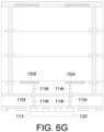
- FIGS. 6A to 6G illustrate manufacturing processes of the semiconductor package 100 of FIG. 1A .
- the first wall 141 is formed in the first layer 131.
- the first layer 131 has the dielectric lower surface 130b and an upper surface 131u opposite to the dielectric lower surface 130b.
- the first wall 141 extends to the upper surface 131u from the dielectric lower surface 130b.
- the first pad 144 is formed on the first wall 141.
- the second layer 132 covering the first pad 144 is formed on the upper surface 131u of the first layer 131. Then, the second wall 142 extending to the first pad 144 from an upper surface 132u of the second layer 132 is formed in the second layer 132.
- the third layer 133 having the dielectric upper surface 130u is formed on the upper surface 132u of the second layer 132. Then, the third wall 143 extending to the second pad 145 from the dielectric upper surface 130u is formed.
- the FSS antenna 160 including the transmitting antenna 160t and the receiving antenna 160r is formed on the dielectric upper surface 130u of the third layer 133.
- the insulation layer 165 covering the FSS antenna 160 is formed on the dielectric upper surface 130u of the third layer 133.
- the transmitting antenna 150t, the receiving antenna 150r and the grounding pad 110g3 is formed on the dielectric lower surface 130b of the first layer 131. Then, the first substrate layer 111 covering the transmitting antenna 150t, the receiving antenna 150r and the grounding pad 110g3 is formed on the dielectric lower surface 130b of the first layer 131.
- the shielding portion 110g1, at least one transmitting portion 114t and at least one receiving portion 114r are formed in the first substrate layer 111, wherein the shielding portion 110g1 extends to the grounding pad 110g3 from the lower surface 111b of the first substrate layer 111, the transmitting portion 114t extends to the transmitting antenna 150t from the lower surface 111b, and the receiving portion 114r extends to the receiving antenna 150r from the lower surface 111b of the first substrate layer 111.
- the grounding layer 110g2 having the first through hole 110g21 and the second through hole 110g22 is formed on the lower surface 111b of the first substrate layer 111.
- the transmitting pad 110t electrically connected to the transmitting portion 114t and the receiving pad 110r electrically connected to the receiving portion 114r are formed within the first through hole 110g21 and the second through hole 110g22 respectively.
- the second substrate layer 112 having a lower surface 112b is formed to cover the grounding layer 110g2, the transmitting pad 110t and the receiving pad 110r. Then, the conductive layer 113 is formed on the lower surface 112b.
- the electronic component 120 is disposed on the conductive layer 113 for being electrically connected to the transmitting antenna 150t through the transmitting portion 114t and the transmitting pad 110t, and being electrically connected to the receiving antenna 150r through the receiving portion 114 and the receiving pad 110r.
- a plurality of contacts 170 are formed on the conductive layer 113 to form the semiconductor package 100 of FIG. 1A .
- FIGS. 7A to 7F illustrate manufacturing processes of the semiconductor package 200 of FIG. 2A .
- the substrate 210 is provided.
- the substrate 210 includes the grounding layer 110g2, the transmitting pad 110t, the receiving pad 110r, the first substrate layer 111, the second substrate layer 112, the conductive layer 113, at least one transmitting portion 114t, at least one receiving portion 114r, at least one transmitting portion 214t and at least one receiving portion 214r.
- the substrate 210 is, for example, an interposer substrate.
- the transmitting antenna 150t and the receiving antenna 150r, respectively, electrically connected to the transmitting portion 214t and the receiving portion 214r are formed in the first substrate layer 111 of the substrate 210.
- the first adhesion 215 covering the transmitting antenna 150t and the receiving antenna 150r is formed on the first substrate layer 111.
- the electronic component 120 is disposed on the transmitting portion 214t and the receiving portion 214r and electrically connected to the transmitting antenna 150t and the receiving antenna 150r through the transmitting portion 214t and the receiving portion 214.
- the dielectric portion 231 having the upper surface 231u and the lower surface 231b opposite to the upper surface 231u, the second adhesion 232 having the dielectric lower surface 230b and the third adhesion 233 is formed above the first adhesion 215, wherein the second adhesion 232 is formed on the lower surface 231b of the dielectric portion 231, and the third adhesion 233 is formed on the upper surface 231u.
- the dielectric portion 231 surrounds the resonant cavity 231r within which the electronic component 120 is disposed.
- the resonant cavity 231r is, for example, a gas layer (for example, air layer) or a vacuum layer, that is, there is no physical component formed within the resonant cavity 231r.
- the interposer 234 having the dielectric upper surface 230u is formed on the third adhesion 233, wherein the interposer 234 includes the substrate 2341 and the shielding portion 2342 surrounding the lateral surface 2341s of the substrate 2341.
- the shielding portion 2342 is exposed from the interposer 234.
- the shielding portion 2342 is, for example, a closed-ring or a pillar.
- the FSS antenna 160 including the transmitting antenna 160t and the receiving antenna 160r is formed on the dielectric upper surface 230u of the interposer 234.
- the insulation layer 165 covering the FSS antenna 160 is formed on the dielectric upper surface 230u of the interposer 234.
- a plurality of contacts 170 are formed on the conductive layer 113 to form the semiconductor package 200 of FIG. 2A .
- FIGS. 8A to 8C illustrate manufacturing processes of the semiconductor package 300 of FIG. 3A.
- the substrate 310 is provided.
- the substrate 310 includes at least one shielding portion 110g1, the grounding layer 110g2, at least one grounding pad 110g3, at least one grounding portion 110g4, the transmitting pad 110t, the receiving pad 110r, the first substrate layer 111, the second substrate layer 112, the conductive layer 113, at least one transmitting portion 114t, at least one receiving portion 114r, at least one transmitting portion 214t and at least one receiving portion 214r.
- the substrate 310 is, for example, an interposer substrate.
- the transmitting antenna 150t and the receiving antenna 150r, respectively, electrically connected to the transmitting portion 214t and the receiving portion 214r are formed in the first substrate layer 111 of the substrate 310.
- the electronic component 120 is disposed on the transmitting portion 214t and the receiving portion 214r and electrically connected to the transmitting antenna 150t and the receiving antenna 150r through the transmitting portion 214t and the receiving portion 214.
- the shielding wall 340 surrounding the resonant cavity 340r is disposed on the substrate 310 within which the electronic component 120 is disposed.
- the dielectric layer 330 including the substrate 331 and the shielding portion 332 surrounding the lateral surface 331s of the substrate 331 is disposed on the shielding wall 340, wherein the shielding portion 332 is electrically connected to the shielding wall 340.
- the FSS antenna 160 including the transmitting antenna 160t and the receiving antenna 160r is formed on the dielectric upper surface 331u of the substrate 331.
- the insulation layer 165 covering the FSS antenna 160 is formed on the dielectric upper surface 331u of the substrate 331.
- a plurality of contacts 170 are formed on the conductive layer 113 to form the semiconductor package 300 of FIG. 3A.
- FIGS. 9A to 9C illustrate manufacturing processes of the semiconductor package 400 of FIG. 4A .
- the substrate 410 is provided.
- the substrate 410 includes at least one shielding portion 110g1, the grounding layer 110g2, at least one grounding pad 110g3, at least one grounding portion 110g4, the transmitting pad 110t, the receiving pad 110r, the first substrate layer 111, the second substrate layer 112, the conductive layer 113, at least one transmitting portion 114t, at least one receiving portion 114r, at least one transmitting portion 214t, at least one receiving portion 214r.
- the substrate 410 is, for example, an interposer substrate.
- the transmitting antenna 150t and the receiving antenna 150r respectively, electrically connected to the transmitting portion 214t and the receiving portion 214r are formed in the first substrate layer 111 of the substrate 410. Then, the first adhesion 415 and the grounding pad 416g covering the transmitting antenna 150t and the receiving antenna 150r are formed on the first substrate layer 111.
- the electronic component 120 is disposed on and electrically connected to the receiving portion 214r and the receiving portion 214r 5.
- the dielectric layer 430 is disposed on the first adhesion 415 of the substrate 410.
- the dielectric layer 430 includes the dielectric portion 431 having the upper surface 431u and the lower surface 431b opposite to the upper surface 431u, the second adhesion 432 formed on the lower surface 431b, the third adhesion 433 formed on the upper surface 431u, the first grounding pad 433g1 and the second grounding pad 433g2.
- the interposer 434 including the substrate 4341, the shielding portion 4342, the fourth adhesion 4343 and the grounding pad 4344g.
- the shielding portion 4342 is embedded in the substrate 4341 and electrically connected to the grounding pad 4344g.
- the shielding portion 4342 is a closed-ring or a pillar.
- the shielding portion 4342 is electrically connected to the shielding wall 440 through the grounding pad 4344g and the second grounding pad 433g2 connected to the shielding wall 440.
- the FSS antenna 160 including the transmitting antenna 160t and the receiving antenna 160r is formed on a dielectric upper surface 4341u of the substrate 4341.
- a plurality of contacts 170 are formed on the conductive layer 113 to form the semiconductor package 400 of FIG. 4A .
- FIGS. 10A to 10K illustrate manufacturing processes of the semiconductor package 500 of FIG. 5A .
- a carrier 510' is formed, wherein the carrier 510' includes the first substrate layer 111, the transmitting portion 114t, the receiving portion 114r, the grounding layer 110g2, the transmitting pad 110t, the receiving pad 110r and the carrier layer 1121 of the second substrate layer 112.
- the carrier layer 1121 covers the grounding layer 110g2, the transmitting pad 110t and the receiving pad 110r.
- the transmitting portion 114t and the receiving portion 114r are embedded in the first substrate layer 111, wherein the transmitting portion 114t is electrically to the transmitting pad 110t, and the receiving portion 114r is electrically to the receiving pad 110r.
- the carrier 510' has a thickness with enough strength.
- the electronic component 120 including at least one contact 121 is disposed on the carrier layer 1121. Then, the covering layer 1122 of the second substrate layer 112 is formed to encapsulate the electronic component 120.
- At least one opening 1122a is formed to expose the contacts 121 of the electronic component 120.
- the grounding portion 110g4, at least one transmitting portion 114t and at least one receiving portion 114r are formed to pass through the carrier layer 1121 and the covering layer 1122, wherein the grounding portion 110g4 extend to the grounding layer 110g2 from the conductive layer 113, the transmitting portion 114t extend to the transmitting pad 110t from the conductive layer 113, and the receiving portion 114r extend to the receiving pad 110r from the conductive layer 113.
- the first substrate layer 111 is removed to expose the edge portion 110ge of the grounding layer 110g2. After being removed, the first substrate layer 111 has the lateral surface 111s.
- the transmitting antenna 150t and the receiving antenna 150r are formed to be electrically connected to the transmitting portion 114t and the receiving portion 114r respectively.
- the dielectric layer 530 encapsulating the transmitting antenna 150t and the receiving antenna 150r is formed on the substrate upper surface 111u of the first substrate layer 111.
- the dielectric layer 530 has the lateral surface 530s, wherein the lateral surface 530s and the lateral surface 111s are aligned with or flush with each other.
- the shielding wall 540 covering the lateral surface 530s, the lateral surface 111s and an dielectric upper surface 530u of the dielectric layer 530 is formed.
- a portion of the shielding wall 540 is removed to expose the dielectric upper surface 530u of the dielectric layer 530.
- the FSS antenna 160 including the transmitting antenna 160t and the receiving antenna 160r is formed on the dielectric upper surface 530u of the dielectric layer 530.
- the insulation layer 165 covering the FSS antenna 160 is formed on the dielectric upper surface 530u of the dielectric layer 530.
- a plurality of contacts 170 are formed on the conductive layer 113 to form the semiconductor package 500 of FIG. 5A .
Landscapes
- Engineering & Computer Science (AREA)
- Microelectronics & Electronic Packaging (AREA)
- Physics & Mathematics (AREA)
- Condensed Matter Physics & Semiconductors (AREA)
- General Physics & Mathematics (AREA)
- Computer Hardware Design (AREA)
- Power Engineering (AREA)
- Electromagnetism (AREA)
- Variable-Direction Aerials And Aerial Arrays (AREA)
- Details Of Aerials (AREA)
- Geometry (AREA)
Claims (9)
- Halbleitergehäuse (200, 400), aufweisend:ein Substrat (210, 410);eine Elektronikkomponente (120), die auf dem Substrat (210, 410) angeordnet und elektrisch mit ihm verbunden ist;eine dielektrische Schicht (230, 430), die eine dielektrische obere Oberfläche (230u) aufweist;eine Sendeantenne (150t) und eine Empfangsantenne (150r), die benachbart zu dem Substrat ausgebildet sind, wobei die Sendeantenne eingerichtet ist, ein Funksignal zu senden; undeine FSS-, frequenzselektive-Oberflächen-, Antenne (160), die benachbart zu der dielektrischen oberen Oberfläche (230u) der dielektrischen Schicht ausgebildet ist;wobei die FSS-Antenne (160) in einer Funksignalabstrahlrichtung durch die dielektrische Schicht von dem Substrat getrennt ist,eine Abschirmwand (240, 440), die in der dielektrischen Schicht eingebettet ist und sich zwischen einer dielektrischen unteren Oberfläche (230b) der dielektrischen Schicht und der dielektrischen oberen Oberfläche (230u) der dielektrischen Schicht erstreckt,wobei die dielektrische Schicht einen dielektrischen Teilbereich (231, 431) aufweist, der eine resonierende Aushöhlung (231r, 431r) umgibt, in welcher die elektronische Komponente (120) angeordnet ist, undwobei die FSS-Antenne (160) in der Funksignalabstrahlrichtung durch den dielektrischen Teilbereich (231, 431) von dem Substrat getrennt ist und die Elektronikkomponente (120) in der resonierenden Aushöhlung (231r, 431r) exponiert ist.
- Halbleitergehäuse gemäß Anspruch 1, wobei die Abschirmwand als ein geschlossener Ring geformt ist.
- Halbleitergehäuse gemäß Anspruch 2, dadurch gekennzeichnet, dass das Substrat weiter aufweist:
eine mit Masse verbindende Kontaktstelle (110g3), die mit der Abschirmwand verbunden ist und die Sendeantenne (150t) und die Empfangsantenne (150r) umgibt. - Halbleitergehäuse gemäß Anspruch 3, dadurch gekennzeichnet, dass das Substrat weiter aufweist:eine mit Masse verbindende Schicht (110g2), die auf einer dielektrischen unteren Oberfläche der dielektrischen Schicht gegenüber der dielektrischen oberen Oberfläche ausgebildet ist;einen mit Masse verbindenden Teilbereich (110g4), der die mit Masse verbindende Kontaktstelle (110g3) mit der mit Masse verbindenden Schicht (110g2) verbindet.
- Halbleitergehäuse gemäß Anspruch 1, wobei die Abschirmwand, die auf einer dielektrischen unteren Oberfläche der dielektrischen Schicht angeordnet ist, die resonierende Aushöhlung (231r, 431r) umgibt, in welcher die Elektronikkomponente (120) angeordnet ist.
- Halbleitergehäuse gemäß Anspruch 1, dadurch gekennzeichnet, dass die dielektrische Schicht ein physikalisches Material ist und die Sendeantenne (150t) und die Empfangsantenne (150r) bezüglich der dielektrischen unteren Oberfläche der dielektrischen Schicht vorstehen.
- Halbleitergehäuse gemäß Anspruch 1, wobei das Substrat aufweist:eine erste Substratschicht (111), die eine seitliche Oberfläche (111s) und eine untere Oberfläche (111b) aufweist;eine mit Masse verbindende Schicht (110g2), die auf der unteren Oberfläche (111b) ausgebildet ist; wobeidie Abschirmwand auf der seitlichen Oberfläche (111s) der ersten Substratschicht (111) ausgebildet ist und sich zu der mit Masse verbindenden Schicht (110g2) erstreckt.
- Halbleitergehäuse gemäß Anspruch 7, dadurch gekennzeichnet, dass das Substrat weiter aufweist:
eine zweite Substratschicht (112), die auf der ersten Substratschicht (111) ausgebildet ist und die Elektronikkomponente (120) umschließt. - Halbleitergehäuse gemäß Anspruch 1, dadurch gekennzeichnet, dass das Substrat weiter aufweist:eine mit Masse verbindende Schicht (110g2), die in dem Substrat ausgebildet ist und ein erstes Durchgangsloch (110g21) und ein zweites Durchgangsloch (110g22) aufweist;eine Sendekontaktstelle (110t), die in dem ersten Durchgangsloch (110g21) angeordnet ist; undeine Empfangskontaktstelle (110r) in dem zweiten Durchgangsloch (110g22);wobei die Sendeantenne (150t) durch die Sendekontaktstelle (110t) elektrisch mit der Elektronikkomponente (120) verbunden ist und die Empfangsantenne (150r) durch die zweite Empfangskontaktstelle (110r) elektrisch mit der Elektronikkomponente (120) verbunden ist.
Applications Claiming Priority (2)
| Application Number | Priority Date | Filing Date | Title |
|---|---|---|---|
| US201962862752P | 2019-06-18 | 2019-06-18 | |
| US16/699,851 US11244913B2 (en) | 2019-06-18 | 2019-12-02 | Semiconductor package |
Publications (2)
| Publication Number | Publication Date |
|---|---|
| EP3754782A1 EP3754782A1 (de) | 2020-12-23 |
| EP3754782B1 true EP3754782B1 (de) | 2024-08-07 |
Family
ID=69410902
Family Applications (1)
| Application Number | Title | Priority Date | Filing Date |
|---|---|---|---|
| EP19218054.5A Active EP3754782B1 (de) | 2019-06-18 | 2019-12-19 | Halbleitergehäuse |
Country Status (4)
| Country | Link |
|---|---|
| US (1) | US11244913B2 (de) |
| EP (1) | EP3754782B1 (de) |
| CN (1) | CN112103622A (de) |
| TW (1) | TWI722913B (de) |
Families Citing this family (5)
| Publication number | Priority date | Publication date | Assignee | Title |
|---|---|---|---|---|
| US11581273B2 (en) * | 2019-12-26 | 2023-02-14 | Advanced Semiconductor Engineering, Inc. | Semiconductor device package and method of manufacturing the same |
| CN116454612A (zh) * | 2022-01-14 | 2023-07-18 | 联发科技股份有限公司 | 天线模块及用于制造天线模块的方法 |
| CN114498001A (zh) * | 2022-01-26 | 2022-05-13 | 华南理工大学 | 基于叠层超表面的毫米波宽角扫描相控阵列天线及通信设备 |
| EP4343971A1 (de) * | 2022-09-26 | 2024-03-27 | Nxp B.V. | Antenneneinheit und verfahren zur herstellung einer antenneneinheit |
| US12424762B2 (en) * | 2023-04-13 | 2025-09-23 | Advanced Semiconductor Engineering, Inc. | Antenna package structure |
Family Cites Families (15)
| Publication number | Priority date | Publication date | Assignee | Title |
|---|---|---|---|---|
| JP3973402B2 (ja) * | 2001-10-25 | 2007-09-12 | 株式会社日立製作所 | 高周波回路モジュール |
| US7728774B2 (en) | 2008-07-07 | 2010-06-01 | International Business Machines Corporation | Radio frequency (RF) integrated circuit (IC) packages having characteristics suitable for mass production |
| CN102130371B (zh) * | 2010-01-19 | 2014-07-02 | 光宝科技股份有限公司 | 应用于移动装置的内藏式调频发射天线 |
| US9190738B2 (en) * | 2010-04-11 | 2015-11-17 | Broadcom Corporation | Projected artificial magnetic mirror |
| US9153542B2 (en) | 2012-08-01 | 2015-10-06 | Advanced Semiconductor Engineering, Inc. | Semiconductor package having an antenna and manufacturing method thereof |
| US9728853B2 (en) | 2014-10-14 | 2017-08-08 | Mediatek Inc. | Antenna structure |
| US9230900B1 (en) | 2014-12-18 | 2016-01-05 | Intel Corporation | Ground via clustering for crosstalk mitigation |
| WO2017209761A1 (en) | 2016-06-03 | 2017-12-07 | Intel IP Corporation | Wireless module with antenna package and cap package |
| US10910329B2 (en) * | 2017-05-23 | 2021-02-02 | Advanced Semiconductor Engineering, Inc. | Semiconductor package device and method of manufacturing the same |
| US10510693B2 (en) * | 2017-09-28 | 2019-12-17 | Taiwan Semiconductor Manufacturing Co., Ltd. | Semiconductor package structure |
| DE112017007887T5 (de) * | 2017-09-29 | 2020-05-07 | Intel Corporation | Antennenpackage mit kugel-anbringungs-array zum verbinden von antennen- und basissubstraten |
| US11322823B2 (en) | 2017-10-17 | 2022-05-03 | Mediatek Inc. | Antenna-in-package with frequency-selective surface structure |
| US10700410B2 (en) * | 2017-10-27 | 2020-06-30 | Mediatek Inc. | Antenna-in-package with better antenna performance |
| KR102022353B1 (ko) * | 2018-01-18 | 2019-09-18 | 삼성전기주식회사 | 안테나 모듈 |
| DE102018205670A1 (de) * | 2018-04-13 | 2019-10-17 | Fraunhofer-Gesellschaft zur Förderung der angewandten Forschung e.V. | Hermetisch abgedichtete Moduleinheit mit integrierten Antennen |
-
2019
- 2019-12-02 US US16/699,851 patent/US11244913B2/en active Active
- 2019-12-19 EP EP19218054.5A patent/EP3754782B1/de active Active
-
2020
- 2020-05-29 CN CN202010482167.1A patent/CN112103622A/zh active Pending
- 2020-06-01 TW TW109118237A patent/TWI722913B/zh active
Also Published As
| Publication number | Publication date |
|---|---|
| CN112103622A (zh) | 2020-12-18 |
| EP3754782A1 (de) | 2020-12-23 |
| US11244913B2 (en) | 2022-02-08 |
| TWI722913B (zh) | 2021-03-21 |
| US20200402931A1 (en) | 2020-12-24 |
| TW202101696A (zh) | 2021-01-01 |
Similar Documents
| Publication | Publication Date | Title |
|---|---|---|
| EP3754782B1 (de) | Halbleitergehäuse | |
| CN103400829B (zh) | 半导体封装件及其制造方法 | |
| US9899335B2 (en) | Method for fabricating package structure | |
| CN108231750B (zh) | 射频器件封装体及其形成方法 | |
| CN104037166B (zh) | 包含天线层的半导体封装件及其制造方法 | |
| CN104051440B (zh) | 具有天线的半导体结构 | |
| US9614277B2 (en) | Radiofrequency module | |
| US6770955B1 (en) | Shielded antenna in a semiconductor package | |
| US5397917A (en) | Semiconductor package capable of spreading heat | |
| US6057601A (en) | Heat spreader with a placement recess and bottom saw-teeth for connection to ground planes on a thin two-sided single-core BGA substrate | |
| US20200118949A1 (en) | Semiconductor package with antenna | |
| KR101991644B1 (ko) | 전자 장치 및 그 제조 방법 | |
| US20170278830A1 (en) | Semiconductor packages having reduced stress | |
| US20120038054A1 (en) | Impedance controlled electrical interconnection employing meta-materials | |
| CN104037137A (zh) | 包括天线基板的半导体封装件及其制造方法 | |
| JP2001516978A (ja) | シールドされた弾性表面波パッケージ | |
| JP2019212979A (ja) | 無線モジュールおよびその製造方法並びに電子装置 | |
| CN108269790B (zh) | 具有集成天线的封装的装置 | |
| EP1263043A1 (de) | Elektronisches Element mit Abschirmung | |
| JP2009295862A (ja) | 高周波樹脂パッケージ | |
| KR20210096578A (ko) | 안테나 모듈 | |
| JP2018186488A (ja) | 配線基板およびrfidモジュール | |
| KR101741648B1 (ko) | 전자파 차폐 수단을 갖는 반도체 패키지 및 그 제조 방법 | |
| US7352056B2 (en) | Semiconductor package structure with microstrip antennan | |
| US12148980B2 (en) | Semiconductor device package and method of manufacturing the same |
Legal Events
| Date | Code | Title | Description |
|---|---|---|---|
| PUAI | Public reference made under article 153(3) epc to a published international application that has entered the european phase |
Free format text: ORIGINAL CODE: 0009012 |
|
| STAA | Information on the status of an ep patent application or granted ep patent |
Free format text: STATUS: REQUEST FOR EXAMINATION WAS MADE |
|
| 17P | Request for examination filed |
Effective date: 20191219 |
|
| AK | Designated contracting states |
Kind code of ref document: A1 Designated state(s): AL AT BE BG CH CY CZ DE DK EE ES FI FR GB GR HR HU IE IS IT LI LT LU LV MC MK MT NL NO PL PT RO RS SE SI SK SM TR |
|
| AX | Request for extension of the european patent |
Extension state: BA ME |
|
| RBV | Designated contracting states (corrected) |
Designated state(s): AL AT BE BG CH CY CZ DE DK EE ES FI FR GB GR HR HU IE IS IT LI LT LU LV MC MK MT NL NO PL PT RO RS SE SI SK SM TR |
|
| STAA | Information on the status of an ep patent application or granted ep patent |
Free format text: STATUS: EXAMINATION IS IN PROGRESS |
|
| 17Q | First examination report despatched |
Effective date: 20220317 |
|
| P01 | Opt-out of the competence of the unified patent court (upc) registered |
Effective date: 20230607 |
|
| GRAP | Despatch of communication of intention to grant a patent |
Free format text: ORIGINAL CODE: EPIDOSNIGR1 |
|
| STAA | Information on the status of an ep patent application or granted ep patent |
Free format text: STATUS: GRANT OF PATENT IS INTENDED |
|
| INTG | Intention to grant announced |
Effective date: 20240301 |
|
| GRAS | Grant fee paid |
Free format text: ORIGINAL CODE: EPIDOSNIGR3 |
|
| GRAA | (expected) grant |
Free format text: ORIGINAL CODE: 0009210 |
|
| STAA | Information on the status of an ep patent application or granted ep patent |
Free format text: STATUS: THE PATENT HAS BEEN GRANTED |
|
| AK | Designated contracting states |
Kind code of ref document: B1 Designated state(s): AL AT BE BG CH CY CZ DE DK EE ES FI FR GB GR HR HU IE IS IT LI LT LU LV MC MK MT NL NO PL PT RO RS SE SI SK SM TR |
|
| REG | Reference to a national code |
Ref country code: GB Ref legal event code: FG4D |
|
| REG | Reference to a national code |
Ref country code: CH Ref legal event code: EP |
|
| REG | Reference to a national code |
Ref country code: IE Ref legal event code: FG4D |
|
| REG | Reference to a national code |
Ref country code: DE Ref legal event code: R096 Ref document number: 602019056491 Country of ref document: DE |
|
| REG | Reference to a national code |
Ref country code: LT Ref legal event code: MG9D |
|
| REG | Reference to a national code |
Ref country code: NL Ref legal event code: MP Effective date: 20240807 |
|
| PG25 | Lapsed in a contracting state [announced via postgrant information from national office to epo] |
Ref country code: NO Free format text: LAPSE BECAUSE OF FAILURE TO SUBMIT A TRANSLATION OF THE DESCRIPTION OR TO PAY THE FEE WITHIN THE PRESCRIBED TIME-LIMIT Effective date: 20241107 |
|
| REG | Reference to a national code |
Ref country code: AT Ref legal event code: MK05 Ref document number: 1711977 Country of ref document: AT Kind code of ref document: T Effective date: 20240807 |
|
| PG25 | Lapsed in a contracting state [announced via postgrant information from national office to epo] |
Ref country code: NL Free format text: LAPSE BECAUSE OF FAILURE TO SUBMIT A TRANSLATION OF THE DESCRIPTION OR TO PAY THE FEE WITHIN THE PRESCRIBED TIME-LIMIT Effective date: 20240807 Ref country code: PT Free format text: LAPSE BECAUSE OF FAILURE TO SUBMIT A TRANSLATION OF THE DESCRIPTION OR TO PAY THE FEE WITHIN THE PRESCRIBED TIME-LIMIT Effective date: 20241209 Ref country code: GR Free format text: LAPSE BECAUSE OF FAILURE TO SUBMIT A TRANSLATION OF THE DESCRIPTION OR TO PAY THE FEE WITHIN THE PRESCRIBED TIME-LIMIT Effective date: 20241108 Ref country code: FI Free format text: LAPSE BECAUSE OF FAILURE TO SUBMIT A TRANSLATION OF THE DESCRIPTION OR TO PAY THE FEE WITHIN THE PRESCRIBED TIME-LIMIT Effective date: 20240807 Ref country code: PL Free format text: LAPSE BECAUSE OF FAILURE TO SUBMIT A TRANSLATION OF THE DESCRIPTION OR TO PAY THE FEE WITHIN THE PRESCRIBED TIME-LIMIT Effective date: 20240807 |
|
| PG25 | Lapsed in a contracting state [announced via postgrant information from national office to epo] |
Ref country code: BG Free format text: LAPSE BECAUSE OF FAILURE TO SUBMIT A TRANSLATION OF THE DESCRIPTION OR TO PAY THE FEE WITHIN THE PRESCRIBED TIME-LIMIT Effective date: 20240807 |
|
| PG25 | Lapsed in a contracting state [announced via postgrant information from national office to epo] |
Ref country code: LV Free format text: LAPSE BECAUSE OF FAILURE TO SUBMIT A TRANSLATION OF THE DESCRIPTION OR TO PAY THE FEE WITHIN THE PRESCRIBED TIME-LIMIT Effective date: 20240807 |
|
| PG25 | Lapsed in a contracting state [announced via postgrant information from national office to epo] |
Ref country code: AT Free format text: LAPSE BECAUSE OF FAILURE TO SUBMIT A TRANSLATION OF THE DESCRIPTION OR TO PAY THE FEE WITHIN THE PRESCRIBED TIME-LIMIT Effective date: 20240807 Ref country code: IS Free format text: LAPSE BECAUSE OF FAILURE TO SUBMIT A TRANSLATION OF THE DESCRIPTION OR TO PAY THE FEE WITHIN THE PRESCRIBED TIME-LIMIT Effective date: 20241207 |
|
| PG25 | Lapsed in a contracting state [announced via postgrant information from national office to epo] |
Ref country code: HR Free format text: LAPSE BECAUSE OF FAILURE TO SUBMIT A TRANSLATION OF THE DESCRIPTION OR TO PAY THE FEE WITHIN THE PRESCRIBED TIME-LIMIT Effective date: 20240807 |
|
| PG25 | Lapsed in a contracting state [announced via postgrant information from national office to epo] |
Ref country code: RS Free format text: LAPSE BECAUSE OF FAILURE TO SUBMIT A TRANSLATION OF THE DESCRIPTION OR TO PAY THE FEE WITHIN THE PRESCRIBED TIME-LIMIT Effective date: 20241107 Ref country code: ES Free format text: LAPSE BECAUSE OF FAILURE TO SUBMIT A TRANSLATION OF THE DESCRIPTION OR TO PAY THE FEE WITHIN THE PRESCRIBED TIME-LIMIT Effective date: 20240807 |
|
| PG25 | Lapsed in a contracting state [announced via postgrant information from national office to epo] |
Ref country code: RS Free format text: LAPSE BECAUSE OF FAILURE TO SUBMIT A TRANSLATION OF THE DESCRIPTION OR TO PAY THE FEE WITHIN THE PRESCRIBED TIME-LIMIT Effective date: 20241107 Ref country code: PT Free format text: LAPSE BECAUSE OF FAILURE TO SUBMIT A TRANSLATION OF THE DESCRIPTION OR TO PAY THE FEE WITHIN THE PRESCRIBED TIME-LIMIT Effective date: 20241209 Ref country code: PL Free format text: LAPSE BECAUSE OF FAILURE TO SUBMIT A TRANSLATION OF THE DESCRIPTION OR TO PAY THE FEE WITHIN THE PRESCRIBED TIME-LIMIT Effective date: 20240807 Ref country code: NO Free format text: LAPSE BECAUSE OF FAILURE TO SUBMIT A TRANSLATION OF THE DESCRIPTION OR TO PAY THE FEE WITHIN THE PRESCRIBED TIME-LIMIT Effective date: 20241107 Ref country code: NL Free format text: LAPSE BECAUSE OF FAILURE TO SUBMIT A TRANSLATION OF THE DESCRIPTION OR TO PAY THE FEE WITHIN THE PRESCRIBED TIME-LIMIT Effective date: 20240807 Ref country code: LV Free format text: LAPSE BECAUSE OF FAILURE TO SUBMIT A TRANSLATION OF THE DESCRIPTION OR TO PAY THE FEE WITHIN THE PRESCRIBED TIME-LIMIT Effective date: 20240807 Ref country code: IS Free format text: LAPSE BECAUSE OF FAILURE TO SUBMIT A TRANSLATION OF THE DESCRIPTION OR TO PAY THE FEE WITHIN THE PRESCRIBED TIME-LIMIT Effective date: 20241207 Ref country code: HR Free format text: LAPSE BECAUSE OF FAILURE TO SUBMIT A TRANSLATION OF THE DESCRIPTION OR TO PAY THE FEE WITHIN THE PRESCRIBED TIME-LIMIT Effective date: 20240807 Ref country code: GR Free format text: LAPSE BECAUSE OF FAILURE TO SUBMIT A TRANSLATION OF THE DESCRIPTION OR TO PAY THE FEE WITHIN THE PRESCRIBED TIME-LIMIT Effective date: 20241108 Ref country code: FI Free format text: LAPSE BECAUSE OF FAILURE TO SUBMIT A TRANSLATION OF THE DESCRIPTION OR TO PAY THE FEE WITHIN THE PRESCRIBED TIME-LIMIT Effective date: 20240807 Ref country code: ES Free format text: LAPSE BECAUSE OF FAILURE TO SUBMIT A TRANSLATION OF THE DESCRIPTION OR TO PAY THE FEE WITHIN THE PRESCRIBED TIME-LIMIT Effective date: 20240807 Ref country code: BG Free format text: LAPSE BECAUSE OF FAILURE TO SUBMIT A TRANSLATION OF THE DESCRIPTION OR TO PAY THE FEE WITHIN THE PRESCRIBED TIME-LIMIT Effective date: 20240807 Ref country code: AT Free format text: LAPSE BECAUSE OF FAILURE TO SUBMIT A TRANSLATION OF THE DESCRIPTION OR TO PAY THE FEE WITHIN THE PRESCRIBED TIME-LIMIT Effective date: 20240807 |
|
| PG25 | Lapsed in a contracting state [announced via postgrant information from national office to epo] |
Ref country code: DK Free format text: LAPSE BECAUSE OF FAILURE TO SUBMIT A TRANSLATION OF THE DESCRIPTION OR TO PAY THE FEE WITHIN THE PRESCRIBED TIME-LIMIT Effective date: 20240807 Ref country code: SM Free format text: LAPSE BECAUSE OF FAILURE TO SUBMIT A TRANSLATION OF THE DESCRIPTION OR TO PAY THE FEE WITHIN THE PRESCRIBED TIME-LIMIT Effective date: 20240807 Ref country code: RO Free format text: LAPSE BECAUSE OF FAILURE TO SUBMIT A TRANSLATION OF THE DESCRIPTION OR TO PAY THE FEE WITHIN THE PRESCRIBED TIME-LIMIT Effective date: 20240807 |
|
| PG25 | Lapsed in a contracting state [announced via postgrant information from national office to epo] |
Ref country code: EE Free format text: LAPSE BECAUSE OF FAILURE TO SUBMIT A TRANSLATION OF THE DESCRIPTION OR TO PAY THE FEE WITHIN THE PRESCRIBED TIME-LIMIT Effective date: 20240807 |
|
| PG25 | Lapsed in a contracting state [announced via postgrant information from national office to epo] |
Ref country code: CZ Free format text: LAPSE BECAUSE OF FAILURE TO SUBMIT A TRANSLATION OF THE DESCRIPTION OR TO PAY THE FEE WITHIN THE PRESCRIBED TIME-LIMIT Effective date: 20240807 |
|
| PG25 | Lapsed in a contracting state [announced via postgrant information from national office to epo] |
Ref country code: SK Free format text: LAPSE BECAUSE OF FAILURE TO SUBMIT A TRANSLATION OF THE DESCRIPTION OR TO PAY THE FEE WITHIN THE PRESCRIBED TIME-LIMIT Effective date: 20240807 |
|
| REG | Reference to a national code |
Ref country code: DE Ref legal event code: R097 Ref document number: 602019056491 Country of ref document: DE |
|
| PLBE | No opposition filed within time limit |
Free format text: ORIGINAL CODE: 0009261 |
|
| STAA | Information on the status of an ep patent application or granted ep patent |
Free format text: STATUS: NO OPPOSITION FILED WITHIN TIME LIMIT |
|
| PG25 | Lapsed in a contracting state [announced via postgrant information from national office to epo] |
Ref country code: MC Free format text: LAPSE BECAUSE OF FAILURE TO SUBMIT A TRANSLATION OF THE DESCRIPTION OR TO PAY THE FEE WITHIN THE PRESCRIBED TIME-LIMIT Effective date: 20240807 |
|
| 26N | No opposition filed |
Effective date: 20250508 |
|
| REG | Reference to a national code |
Ref country code: CH Ref legal event code: PL |
|
| PG25 | Lapsed in a contracting state [announced via postgrant information from national office to epo] |
Ref country code: LU Free format text: LAPSE BECAUSE OF NON-PAYMENT OF DUE FEES Effective date: 20241219 |
|
| PG25 | Lapsed in a contracting state [announced via postgrant information from national office to epo] |
Ref country code: SE Free format text: LAPSE BECAUSE OF FAILURE TO SUBMIT A TRANSLATION OF THE DESCRIPTION OR TO PAY THE FEE WITHIN THE PRESCRIBED TIME-LIMIT Effective date: 20240807 |
|
| REG | Reference to a national code |
Ref country code: BE Ref legal event code: MM Effective date: 20241231 |
|
| PG25 | Lapsed in a contracting state [announced via postgrant information from national office to epo] |
Ref country code: BE Free format text: LAPSE BECAUSE OF NON-PAYMENT OF DUE FEES Effective date: 20241231 |
|
| PG25 | Lapsed in a contracting state [announced via postgrant information from national office to epo] |
Ref country code: CH Free format text: LAPSE BECAUSE OF NON-PAYMENT OF DUE FEES Effective date: 20241231 |
|
| PG25 | Lapsed in a contracting state [announced via postgrant information from national office to epo] |
Ref country code: IE Free format text: LAPSE BECAUSE OF NON-PAYMENT OF DUE FEES Effective date: 20241219 |
|
| PGFP | Annual fee paid to national office [announced via postgrant information from national office to epo] |
Ref country code: DE Payment date: 20250930 Year of fee payment: 7 |
|
| PGFP | Annual fee paid to national office [announced via postgrant information from national office to epo] |
Ref country code: GB Payment date: 20251001 Year of fee payment: 7 |
|
| PGFP | Annual fee paid to national office [announced via postgrant information from national office to epo] |
Ref country code: FR Payment date: 20251008 Year of fee payment: 7 |
|
| PG25 | Lapsed in a contracting state [announced via postgrant information from national office to epo] |
Ref country code: IT Free format text: LAPSE BECAUSE OF FAILURE TO SUBMIT A TRANSLATION OF THE DESCRIPTION OR TO PAY THE FEE WITHIN THE PRESCRIBED TIME-LIMIT Effective date: 20240807 |