EP3751630B1 - Organische elektrolumineszente vorrichtung - Google Patents
Organische elektrolumineszente vorrichtung Download PDFInfo
- Publication number
- EP3751630B1 EP3751630B1 EP19834725.4A EP19834725A EP3751630B1 EP 3751630 B1 EP3751630 B1 EP 3751630B1 EP 19834725 A EP19834725 A EP 19834725A EP 3751630 B1 EP3751630 B1 EP 3751630B1
- Authority
- EP
- European Patent Office
- Prior art keywords
- light
- layer
- energy
- organic
- sacrificial layer
- Prior art date
- Legal status (The legal status is an assumption and is not a legal conclusion. Google has not performed a legal analysis and makes no representation as to the accuracy of the status listed.)
- Active
Links
Images



Classifications
-
- H—ELECTRICITY
- H10—SEMICONDUCTOR DEVICES; ELECTRIC SOLID-STATE DEVICES NOT OTHERWISE PROVIDED FOR
- H10K—ORGANIC ELECTRIC SOLID-STATE DEVICES
- H10K50/00—Organic light-emitting devices
- H10K50/10—OLEDs or polymer light-emitting diodes [PLED]
- H10K50/14—Carrier transporting layers
- H10K50/15—Hole transporting layers
- H10K50/155—Hole transporting layers comprising dopants
-
- H—ELECTRICITY
- H10—SEMICONDUCTOR DEVICES; ELECTRIC SOLID-STATE DEVICES NOT OTHERWISE PROVIDED FOR
- H10K—ORGANIC ELECTRIC SOLID-STATE DEVICES
- H10K50/00—Organic light-emitting devices
- H10K50/10—OLEDs or polymer light-emitting diodes [PLED]
- H10K50/14—Carrier transporting layers
- H10K50/16—Electron transporting layers
- H10K50/165—Electron transporting layers comprising dopants
-
- H—ELECTRICITY
- H10—SEMICONDUCTOR DEVICES; ELECTRIC SOLID-STATE DEVICES NOT OTHERWISE PROVIDED FOR
- H10K—ORGANIC ELECTRIC SOLID-STATE DEVICES
- H10K50/00—Organic light-emitting devices
- H10K50/80—Constructional details
- H10K50/86—Arrangements for improving contrast, e.g. preventing reflection of ambient light
- H10K50/865—Arrangements for improving contrast, e.g. preventing reflection of ambient light comprising light absorbing layers, e.g. light-blocking layers
-
- H—ELECTRICITY
- H10—SEMICONDUCTOR DEVICES; ELECTRIC SOLID-STATE DEVICES NOT OTHERWISE PROVIDED FOR
- H10K—ORGANIC ELECTRIC SOLID-STATE DEVICES
- H10K2101/00—Properties of the organic materials covered by group H10K85/00
- H10K2101/40—Interrelation of parameters between multiple constituent active layers or sublayers, e.g. HOMO values in adjacent layers
-
- H—ELECTRICITY
- H10—SEMICONDUCTOR DEVICES; ELECTRIC SOLID-STATE DEVICES NOT OTHERWISE PROVIDED FOR
- H10K—ORGANIC ELECTRIC SOLID-STATE DEVICES
- H10K2102/00—Constructional details relating to the organic devices covered by this subclass
- H10K2102/301—Details of OLEDs
- H10K2102/331—Nanoparticles used in non-emissive layers, e.g. in packaging layer
-
- H—ELECTRICITY
- H10—SEMICONDUCTOR DEVICES; ELECTRIC SOLID-STATE DEVICES NOT OTHERWISE PROVIDED FOR
- H10K—ORGANIC ELECTRIC SOLID-STATE DEVICES
- H10K2102/00—Constructional details relating to the organic devices covered by this subclass
- H10K2102/301—Details of OLEDs
- H10K2102/351—Thickness
-
- H—ELECTRICITY
- H10—SEMICONDUCTOR DEVICES; ELECTRIC SOLID-STATE DEVICES NOT OTHERWISE PROVIDED FOR
- H10K—ORGANIC ELECTRIC SOLID-STATE DEVICES
- H10K85/00—Organic materials used in the body or electrodes of devices covered by this subclass
- H10K85/30—Coordination compounds
-
- H—ELECTRICITY
- H10—SEMICONDUCTOR DEVICES; ELECTRIC SOLID-STATE DEVICES NOT OTHERWISE PROVIDED FOR
- H10K—ORGANIC ELECTRIC SOLID-STATE DEVICES
- H10K85/00—Organic materials used in the body or electrodes of devices covered by this subclass
- H10K85/60—Organic compounds having low molecular weight
-
- H—ELECTRICITY
- H10—SEMICONDUCTOR DEVICES; ELECTRIC SOLID-STATE DEVICES NOT OTHERWISE PROVIDED FOR
- H10K—ORGANIC ELECTRIC SOLID-STATE DEVICES
- H10K85/00—Organic materials used in the body or electrodes of devices covered by this subclass
- H10K85/60—Organic compounds having low molecular weight
- H10K85/631—Amine compounds having at least two aryl rest on at least one amine-nitrogen atom, e.g. triphenylamine
-
- H—ELECTRICITY
- H10—SEMICONDUCTOR DEVICES; ELECTRIC SOLID-STATE DEVICES NOT OTHERWISE PROVIDED FOR
- H10K—ORGANIC ELECTRIC SOLID-STATE DEVICES
- H10K85/00—Organic materials used in the body or electrodes of devices covered by this subclass
- H10K85/60—Organic compounds having low molecular weight
- H10K85/649—Aromatic compounds comprising a hetero atom
- H10K85/657—Polycyclic condensed heteroaromatic hydrocarbons
- H10K85/6572—Polycyclic condensed heteroaromatic hydrocarbons comprising only nitrogen in the heteroaromatic polycondensed ring system, e.g. phenanthroline or carbazole
Definitions
- the present application relates to the field of lighting, specifically to the field of OLED lighting, in particular to an organic light emitting device.
- OLED Organic light emitting diode
- OLED Organic light emitting diode
- the light-emitting principle of the OLED is using transparent / translucent metal / metal oxide electrodes and metal / metal oxide electrodes as an anode and a cathode of the device, respectively.
- carriers electrons and holes
- Electrons and holes are transferred to the light-emitting layer through the electron transport functional layer and hole transport functional layer, respectively, and an exciton is formed in the light-emitting material.
- the restricted electron-hole in the excitons disappears after recombination, and the energy is radiated in the form of visible light (emission wavelength is limited by the properties of the light-emitting material).
- the radiated light can be observed from the transparent / translucent electrode side. This light-emitting principle is widely used in lighting and display screens.
- OLED devices are sensitive to high-energy light, and light-emitting energy of mainly high-energy light is 2.8-4.1 eV in general environment.
- Some materials in the OLED device may be attenuated by the high-energy light in the environment.
- the rule of attenuation is that the product of the illuminance of the high-energy light and the amount of exposure time is close to a fixed value.
- a certain ratio of attenuation to the original brightness is defined as the lifetime of the OLED lighting. If OLED devices are exposed to a large amount of high-energy light in the applications (such as automotive or aviation lighting), the high-energy light will accelerate the aging process of the panel and shorten its lifetime.
- the industry's common way is to set components outside the panel that can block high-energy light, and reduce the high-energy light entering the OLED device, and alleviate the degradation of the device, such as using an external cover, anti-UV film, and reflective layer, etc., thereby increasing the lifetime of the OLED panel.
- these ways will introduce new materials or components, increase the process and cost, increase the volume and weight of the product, and even bring new risks.
- US 2005/023966 A1 discloses an organic electroluminescent display device comprising a UV stabilizer and provides an organic electroluminescent display device whose characteristics are not degraded by ultraviolet rays even after being exposed to sunlight by providing an organic electroluminescent display device comprising a substrate, a first electrode formed on the substrate, a light emitting layer formed on the first electrode, and a second electrode formed on the upper part of the light emitting layer, wherein the light emitting layer is doped with a UV stabilizer, and the UV stabilizer has an absorption range of 420 nm or less.
- US 2005/062406 A1 discloses an organic EL device, a hole injection electrode (anode) made of a transparent electrode.
- a first hole injection layer made of CuPc, a second hole injection layer made of CFx, a hole transport layer and alight emitting layer each made of an organic material are formed in this order on the hole injection electrode.
- An electron injection electrode (cathode) is further formed on the light emitting layer.
- the first hole injection layer made of CuPc absorbs ultraviolet light, so that the organic EL device can be prevented from deterioration by the ultraviolet light.
- the second hole injection layer made of CFx promotes injection of holes, so that the initial drive voltage can be reduced.
- the present application aims to solve the above problem that provides an organic light emitting device that can substantially improve the resistance of the OLED device to high-energy light irradiation without affecting the appearance design.
- the present application provides an organic light emitting device including a substrate, a first electrode, an organic layer, a second electrode, and a packaging structure that are sequentially stacked;
- the high-energy light sacrificial layer includes the hole transport function layer / electron transport function layer and a light-absorbing material layer located in or on the hole transport function layer / electron transport function layer; the light-absorbing material layer is formed of the light-absorbing material.
- the photoluminescent material is any one of a fluorescent material, a phosphorescent material or a quantum dot light-emitting material.
- the volume percentage of the light-absorbing material in the high-energy light sacrificial layer is more than or equal to 0.1% and less than or equal to 30%.
- the volume percentage of the photoluminescent material in the high-energy light sacrificial layer is more than or equal to 0.1% and less than or equal to 15%.
- the volume percentage of the colored light-absorbing material in the high-energy light sacrificial layer is more than or equal to 0.1% and less than or equal to 10%.
- the volume percentage of the exciton quenching material in the high-energy light sacrificial layer is more than or equal to 2% and less than or equal to 15%.
- the colored light-absorbing material includes at least one of a salicylate, a benzophenone, a benzotriazole, a substituted acrylonitrile, a triazine, a direct dye, a basic dye, an acid dye, a disperse dye, a reactive dye, a sulfur dye, a vat dye and an cationic dye.
- the colored light-absorbing material includes at least one of 2- (2'-xenyl 3', 5'-di-pentylphenyl) benzotriazole and 2-xenyl-4-n-octyloxybenzophenone.
- the material of the first additional functional layer has the same charge transport characteristics as the host material of the high-energy light sacrificial layer.
- the thickness of the first additional function layer is more than or equal to 10 nm and less than or equal to 100 nm.
- the thickness of the high-energy light sacrificial layer is more than or equal to 30 nm and less than or equal to 250 nm.
- the present application provides a method for manufacturing an organic light emitting device, comprising the following steps: a first electrode, a high-energy light sacrificial layer, a first additional function layer, an light-emitting layer, an electron transport function layer or a hole transport function layer, and a second electrode are sequentially formed on a substrate by any way of vacuum thermal evaporation, wet process, inkjet printing technology, spin coating, and slit coating;
- a high-energy light sacrificial layer is provided in a specific position between the light-emitting layer and the electrode layer on the light-emergent face of the organic light emitting device (OLED device), the OLED device is essentially capable of resisting high-energy light, thereby greatly improving the reliability and lifetime of OLED-related products and also increasing the application space.
- the high-energy light sacrificial layer is provided in the hole transport function layer or electron transport function layer, especially when the high-energy light sacrificial layer is the hole transport function layer or the electron transport function layer doped with a light-absorbing material, the light-absorbing material has the function of blocking high-energy light, this solution improve the ability of the OLED device to absorb high-energy light without affecting original structure and production process of the OLED device.
- the light-absorbing material adopts at least one of a photoluminescent material, a colored light-absorbing material, and an exciton quenching material, so that the high-energy light sacrificial layer irradiated absorbs external high-energy light and converts it into low-energy light or converts the energy into phonon dissipation. It can significantly improve the effect of the uneven light-emitting of OLED panel caused by the high-energy light and relieve the voltage rise of OLED panel exposed to the high-energy light for a long time.
- the high-energy light sacrificial layer is provided in the hole transport function layer or electron transport function layer, alternatively, a light-absorbing material layer is located on the hole transport function layer or electron transport function layer; the light-absorbing material layer is formed of light-absorbing material.
- the light-absorbing material in the high-energy light sacrificial layer is mainly selected from at least one of a photoluminescent material, a colored light-absorbing material, and an exciton quenching material.
- the selection of materials is universal and convenient, and its effect on the efficiency of the original OLED device is below 15%.
- the absorption of high-energy light by this layer can relieve the speed of the voltage rise of the OLED panel exposed to the high-energy light for a long time, make the highest point of the voltage rise of the OLED device lower after exposure to the high-energy light. This is because the attenuation effect of the OLED device is characterized by a decrease of brightness and a rise of voltage in terms of photoelectric performance. Reducing the speed of voltage rise and the highest point of voltage rise is equivalent to increasing the lifetime of the panel.
- the test shows that the method of the present application increases the lifetime of the panel by at least 30%.
- a first additional functional layer is provided between the high-energy light sacrificial layer and the light-emitting layer for avoiding electroluminescence, and especially when the additional function layer is made of the host material of the high-energy light sacrificial layer, the effect is better and the process is simpler.
- FIG. 1 is a structural schematic diagram of a first embodiment of an organic light emitting device of the present application.
- the organic light emitting device is an OLED device, including a substrate 10, a first electrode 20, a hole transport function layer 30, a light-emitting layer 40, an electron transport function layer 50, a second electrode 60, and an encapsulation structure (not shown in figure 1 ) that are sequentially stacked; wherein the hole transport function layer 30, the light-emitting layer 40 and the electron transport function layer 50 form an organic layer of the OLED device; wherein the light-emergent face of the organic light emitting device is located on the side of the first electrode 20, a high-energy light sacrificial layer (set in the layer where the diagonal bar is drawn in figure 1 ) is provided between the first electrode 20 and the light-emitting layer 40.
- the high-energy light sacrificial layer is formed by the hole transport function layer 30 as a host material doped with a light-absorbing material; as shown in figure 2 , in this embodiment, the hole transport function layer 30 includes a hole injection layer HI 31, a hole transport layer HT 32 and an electron blocking layer EBL, the high-energy light sacrificial layer 33 is formed by the electron blocking layer EBL doped with light-absorbing material 80.
- the light-absorbing material is made of a photoluminescent material, specifically, is made of a fluorescent material; in other embodiments, the light-absorbing material can also be made of other photoluminescent materials, such as a phosphorescent material or a quantum dot light-emitting material ( quantum dot material).
- the fluorescent material is made of a red fluorescent material.
- the fluorescent material can also be made of a green fluorescent material or a blue fluorescent material, such as C545T ( 2 , 3 , 6 , 7- Tetrahydro -1 , 1 , 7 , 7 , - tetramethyl-1H , 5H , 11H-10- (2-benzothiazolyl) quinolizino [ 9 , 9a , 1gh ] coumarin) , AND (9 , 10 - Di (naphth-2-yl) anthracene) , DBP (Dibenzo ⁇ [ f , f ] -4 , 4' , 7 , 7'-tetraphenyl ⁇ diindeno [ 1 , 2 , 3-cd :1' , 2' , 3'-lm ] perylene) , Rubrene ( 5 , 6 , 11 , 12 - Tetrapheny ln
- the phosphorescent material can be made of Ir ( btp ) 2 ( acac ) ( Bis ( 2 - benzo [ b ] thiophen - 2 - yl - pyridine ) ( acetylacetonate ) iridium ( III ) ), Ir ( mppy ) 3 ( Tris [ 2- ( p -tolyl ) pyridine ] iridium ( III ) ), FIrPic ( Bis ( 3 , 5 - difluoro - 2 - ( 2 - pyridyl ) phenyl - ( 2 - carboxypyridyl ) iridium ( III ) ).
- the quantum dot light-emitting material can be made of perovskite quantum dots
- the normal quantum dot material is the semiconductor nanoparticles which are made of II - VII clan (Cdse, Cds, Znse, Cds, Pbs, Pbse), III - VI clan (InP , InAs), or I - III - VII clan (CuIns2,AgIns2) materials.
- the energy gap of the above photoluminescent material is higher than the energy gap of the light-emitting layer and less than the energy gap of the doped host material of the high-energy light sacrificial layer.
- the above photoluminescent materials will become excited state after absorbing high-energy light. When the energy is transferred from the excited state to the ground state, it is released in the form of luminescence, and this mechanism is called photoluminescence.
- the high-energy light sacrificial layer can also be called color conversion layer.
- the light emission wavelength of most OLED devices is between 450nm-700nm, and the energy gap of the photoluminescent material is higher than that of the light-emitting layer material, the light emitted by OLED will not be absorbed by the photoluminescence material (color conversion layer).
- the volume percentage of the photoluminescent material in the high-energy light sacrificial layer is 10%. In other embodiments, the volume percentage of the photoluminescent material in the high-energy light sacrificial layer is more than or equal to 0.1% and less than or equal to 15%.
- a first additional functional layer 70 for avoiding electroluminescence is provided between the high-energy light sacrificial layer 33 and the light-emitting layer 40.
- the above hole transport function layer 30 is made of a material that have the capability of hole transport.
- the above electron transport function layer 50 is made of a material that have the capability of electron transport.
- a first additional functional layer 70 is provided between the high-energy light sacrificial layer and the light-emitting layer, wherein the material of the first additional functional layer 70 and the host material of the high-energy light sacrificial layer have the same charge transport characteristics, which can ensure that there is only a single type of carrier (electron or hole) in the high-energy light sacrificial layer, and achieving the effect of avoiding electroluminescence.
- the first additional functional layer 70 is the material that can realize the function of hole transport, for example, it can be a different type of EBL, such as EBL1, EBL2, orEBL3 etc..
- FIG. 3 is a structural schematic diagram of a second embodiment of an organic light emitting device of the present application. Like the embodiment 1, in this embodiment, the OLED is also bottom-emitting type. The differences from embodiment 1 are as follows: in this embodiment, an electron transport function layer 50 is provided between the first electrode 20 and the light-emitting layer 40, and the high-energy light sacrificial layer is formed by the electron transport function layer 50 as a host material doped with light-absorbing material, and the first additional functional layer 70 is provided between the electron transport function layer 50 and the light-emitting layer 40 accordingly.
- the electron transport function layer 50 includes a electron injection layer EI 51, a electron transport layer ET 52 and an hole blocking layer HBL 53.
- the light-absorbing material 80 is doped in the hole blocking layer HBL 53.
- the high-energy light sacrificial layer is formed by the hole blocking layer HBL53 doped with light-absorbing material 80; the material of the first additional functional layer 70 also belongs to HBL.
- Figure 5 is a structural schematic diagram of a third embodiment of an organic light emitting device of the present application.
- the OLED is top-emitting type
- the electron transport function layer 50 is provided between the light-emitting layer 40 and the second electrode 60.
- the high-energy light sacrificial layer is formed by the electron transport function layer 50 as a host material doped with light-absorbing material
- the first additional functional layer 70 is provided between the electron transport function layer 50 and the light-emitting layer 40 accordingly.
- FIG. 6 is a structural schematic diagram of a fourth embodiment of an organic light emitting device of the present application. Like the embodiment 3, in this embodiment, the OLED is also top-emitting type. The differences from embodiment 3 are as follows: in this embodiment, the hole transport function layer 30 is provided between the light-emitting layer 40 and the second electrode 60. On this occasion, the high-energy light sacrificial layer is formed by the hole transport function layer 30 as a host material doped with light-absorbing material, and the first additional functional layer 70 is provided between the hole transport function layer 30 and the light-emitting layer 40 accordingly.
- the above embodiments 1 to 4 illustrate that the technical solution of the present application is not only applicable to OLED devices with PIN (hole transport function layer-light emitting layer-electron transport function layer) structure, but also applicable to NIP structures (electron transport function layer-light emitting layer-hole transport function layer) OLED devices, not only applicable to bottom-emitting OLED devices, but also applicable to top-emitting OLED devices.
- PIN hole transport function layer-light emitting layer-electron transport function layer
- NIP structures electroctron transport function layer-light emitting layer-hole transport function layer
- the light-absorbing material 80 is configured separately to form a separate light-absorbing material layer 81, and the light-absorbing material layer 81 is located between the light-emitting layer and the electron blocking layer EBL.
- the light-absorbing material layer 81 is located between the hole injection layer HI31 and the hole transport layer HT32.
- the light-absorbing material layer 81 also can be located between the electron blocking layer EBL and the hole transport layer HT32. Therefore, the definition of the high-energy light sacrificial layer of this application is: one layer of the hole transport function layer doped with the light-absorbing material, or one layer of electron transport function layer doped with the light-absorbing material, or the superimposed layer of the light-absorbing material layer and the one layer of the hole transport function layer which is close to the side of the light-emitting layer and adjacent to the light-absorbing material layer, or the superimposed layer of the light-absorbing material layer and the one layer of the electron transport function layer which is close to the side of the light-emitting layer and adjacent to the light-absorbing material layer.
- the photoluminescent material of the light-absorbing material 80 in the first embodiment is replaced by a colored light-absorbing material, specifically, it is 2- (2'-xenyl 3',5'-di-pentylphenyl) benzotriazole.
- the colored light-absorbing material includes at least one of a salopheicylate, a benznone, a benzotriazole, a substituted acrylonitrile, a triazine, a direct dye, a basic dye, an acid dye, a disperse dye, a reactive dye, a sulfur dye, a vat dye and a cationic dye.
- the direct dye includes, for example, diaminostilbene disulfonic acids, 4.4'-diaminodiphenylureas, 4.4'-diaminobenzoylanilides, 4.4'-diaminobenzenesulfanilides, diaminoheterocyclics, etc., specifically, such as 2- (2'-xenyl 3',5'-di-pentylphenyl) benzotriazole and 2-xenyl-4-n-octyloxybenzophenone.
- the acid dye includes, for example, bromine derivatives etc..
- the colored light-absorbing materials are colored dyes, which can be defined as ultraviolet/near ultraviolet/blue absorbers.
- the colored light-absorbing material can absorb most of the short-wave high-energy light (more than 60%) below 450nm, and the absorbed proportion of the blue waveband of 450-500nm is between 30% and 60%, and the transmittance of the 500nm-750nm wave band (the wave band is also the emission wave band of the light-emitting layer) is above 80%, that is to say, the absorbed proportion is below 20%.
- the volume percentage of the colored light-absorbing material in the high-energy light sacrificial layer is 5%. In other embodiments, the volume percentage of the colored light-absorbing material in the high-energy light sacrificial layer can be more than or equal to 0.1% and less than or equal to 10%.
- the exciton quenching material can form a layer alone.
- an experimental group 1 and an experimental group 2 are the ingredient statements of each layer of the organic layer of the OLED panel in the embodiment provided by this application; an control group 1 is the ingredient statement of each layer of the organic layer of the OLED panel in the existing technology of the this application.
- the experimental group 1 is based on the control group 1, and the yellow fluorescent material (Yellow dopant) is mixed in the HT layer of the control group 1; the experimental group 2 is a yellow fluorescent material layer of 3 nm thickness on the surface of the HT layer in the control group 1; HT (20nm) adjacent to the light-emitting layer is used as the first additional function layer in the experimental groups 1 and 2.
- the electrical parameters of the panel are relatively close to the control group 1, but the lifetime of the panel has been significantly improved.
- the experimental results in the above table 5 indicate that the experimental group 3, which includes an exciton quenching material the p-doped material (F4-TCNQ), showing a significant decrease in operating voltage and a better photoelectric performance when compared with the experimental group 1 at the same brightness.
- F4-TCNQ p-doped material
- control group 2 is the ingredient statement of each layer of the organic layer of the OLED panel of the existing technology
- an experimental group 4 is the ingredient statement of each layer of the organic layer of the OLED panel in one type of the embodiment provided by this application.
- Table 6 Control Group 2 hole injection layer HI (10 nm)/ hole transport layer NPB (70 nm)/ electron blocking layer EBL (10 nm)/ light-emitting layer (35 nm)/ HBL hole blocking layer (10 nm)/ electron transport layer ET (30 nm)
- the structure of the high-energy light sacrificial layer in the above experimental group 4 is NPB: F4-TCNQ: Rubrene, the three are doped according to the optimized ratio; Rubrene is a fluorescent dye.
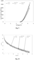
- the two panels of the control group 2 and the experimental group 4 were exposed to simulated sunlight for 1,300 hours, and photoelectric characteristics were measured every 48 hours.
- the experimental results show that the experimental group 4 has stable photoelectric characteristics after long-term irradiation; in the control group 2, the voltage of the same current density increase by 1.7 V due to the influence of irradiation, and nonuniformity occurs based on the area, showing the obvious effect of the high-energy light sacrificial layer.
- mice 5-9 of the control experiment correspond to the embodiments provided in this application.
- the device structure of the OLED panel of each embodiment is ITO-glass / NPB : Rubrene : F4-TCNQ (x nm)/ NPB (250-x nm )/ ET (15nm) / EML / ET / Al, where x is the thickness of the high-energy light sacrificial layer.
- ITO-glass is the first electrode
- NPB:Rubrene:F4-TCNQ (x nm) /NPB (250-x nm) is the hole transport function layer of the doped fluorescent dye Rubrene and the exciton quenching material F4-TCNQ
- ET (15nm) is the first additional functional layer
- EML is the light-emitting layer
- ET is the electron transport function layer
- Al is the second electrode
- the values of x corresponding to the above experimental groups 5-9 are 10 nm, 30 nm, 100 nm, 200 nm, 250 nm, respectively.
- the host material of the high-energy light sacrificial layer in the above experimental groups 5-9 is the hole transport material NPB; the light-absorbing material uses the fluorescent dye Rubrene (the concentration is 2%); the exciton quenching material uses F4-TCNQ (the concentration is 8%).
- This experiment is mainly used to test the effect of different concentrations of exciton quenching materials on the photoelectric performance of the OLED panel.
- experimental groups 10-13 are the ingredient statements of each layer of the organic layer of the OLED panel in the embodiment provided by this application.
- the following "prime” represents the first additional function layer.
- Table 9 is a comparison statement of the photoelectric characteristics of each group of OLED panels corresponding to this control experiment.
- Exciton quenching materials generally have the effect of enhancing the charge transport capability.
- the exciton quenching materials in this experimental group are generally used to improve the charge transport capability; in this technology field, the doping concentration of the material used to enhance the charge transport capability is generally around 2%, which can significantly improve the charge transport capability.
- the structure of the hole transport function layer is m-TDATA:F4-TCNQ (20%, 150nm)
- its optical energy gap decreases from 2.91 to 2.55 electron volts from calculation.
- the color of the film changes from nearly transparent to yellowish by visually check; after preparing the device, the characteristics under irradiation condition are compared; when the OLED panel is irradiated and stored under the simulated sunlight of 1000W/m ⁇ 2 (the ultraviolet intensity at a wavelength of 300nm-400nm is 30W/m ⁇ 2), the stability of the panel is significantly improved, and the voltage has no significant change during the measurement time.
- this experimental group shows that the high concentration of the exciton quenching material doped solely in the hole transport functional layer or electron transport functional layer can not only play the role of exciton quenching, but also play the role of charge boosting, and the excess light-absorbing material can further block high-energy light.
- the doped exciton quenching material causes a large amount of charge present in the doped electron transport function layer and hole transport function layer; there are a large number of excitons in the light-emitting layer in theory, and the excitons dominate the luminous efficiency and luminescent characteristics; however, excitons can easily interact with charges, and this interaction can easily quench the excitons.
- Excitons easily interact with charges, but the formation of excitons also starts with charges (holes and electrons enter into the light-emitting layer respectively, and the excited state before electron and hole's recombination luminescence is called exciton); therefore, the first additional functional layer has the same carrier transport characteristics as the electron transport functional layer or the hole transport functional layer, but the characteristics are worse than the doped layer.
- the first additional function layer designed in the above embodiments of the present application may also be called a protection layer; when the carrier transmission characteristics there of are consistent with the carrier transmission characteristics of the doped transport function layer, the interaction between charge and excitons can be reduced, and the exciton can be confined in the light-emitting layer, avoiding the occurrence of quenching.
- an experimental group 14 and an experimental group 15 are the ingredient statements of each layer of the organic layer of the OLED panel in the embodiment provided by this application; the control group 1 is the ingredient statement of each layer of the organic layer of the OLED panel in the existing technology of the this application.
- Table 10 Experimental Group the Composition of Each Layer of the Organic Layer Control Group 1 HI/HT (40 nm) /light-emitting layer/ET Experimental Group 14 HI/HT: 2- (2'-xenyl 3',5'-di-pentylphenyl) benzotriazole (20 nm) /HT (20 nm) /light-emitting layer/ET Experimental Group 15 HI/HT (17 nm) /2- (2'-xenyl 3',5'-di-pentylphenyl) benzotriazole (3 nm) /HT (20 nm) /light-emitting layer/ET
- 2-(2'-xenyl 3',5'-di-pentylphenyl)benzotriazole can also be replaced by 2-xenyl-4-n-octyloxy benzophenone or other light-absorbing materials.
- the experimental group 14 and an experimental group 16 are the ingredient statements of each layer of the organic layer of the OLED panel in the embodiment provided by this application.
- Table 12 Experimental Group the Composition of Each Layer of the Organic Layer Experimental Group 14 HI/HT: 2-(2'-xenyl 3',5'-di-pentylphenyl)benzotriazole (20 nm) /HT (20 nm) /light-emitting layer/ET
- Experimental Group 16 HI/ HT: 2-(2'-xenyl 3',5'-di-pentylphenyl)benzotriazole (20 nm) : F4-TCNQ/HT (20 nm) /light-emitting layer/ET
- the experimental results in the above table 13 indicate that the experimental group 16, which includes an exciton quenching material, i.e. the p-doped material (F4-TCNQ), shows a significant decrease in operating voltage and a better photoelectric performance when compared with experimental group 14 at the same brightness.
- the photoluminescence phenomenon can be observed in the high-energy light sacrificial layer and the light-emitting layer in the experimental group 14, but the photoluminescence phenomenon can't be observed in the light-emitting layer in the experimental group 16. This shows that most of the ultraviolet light is absorbed and quenched by the high-energy light sacrificial layer; therefore, the experimental group 16 is more effective than the experimental group 14 in protecting the light-emitting layer from high-energy light irradiation.
- the photoluminescent material and the colored light-absorbing material can also be used in the high-energy light sacrificial layer at the same time.
- a fluorescent dye is added to HT: 2-(2'-xenyl 3',5'-di-pentylphenyl)benzotriazole (20nm) layer in the experimental group 14; or a phosphorescent dye is added to HT: 2-(2'-xenyl 3',5'-di-pentylphenyl)benzotriazole (20nm) layer in the experimental group 16.
- the hole injection material commonly used in the industry can be used together with the conventional commercial material NDP-9 and the fluorescent material Rubrene by co-evaporation to obtain the high-energy light sacrificial layer at the side of hole transporting, wherein the high-energy light sacrificial layer adopts a method of absorbing radiation to block high-energy light and improve the hole transport capability.
- the common electron transport material Bphen can also be co-evaporated with a specific ratio of metallic silver to complete the design of the high-energy light sacrificial layer at the side of electron transporting, wherein the high-energy light sacrificial layer adopts Bphen and silver complex to improve the electron transmission characteristics, and some silver atoms do not react with organic molecules, and have the ability to absorb light irradiation.
Landscapes
- Physics & Mathematics (AREA)
- Optics & Photonics (AREA)
- Electroluminescent Light Sources (AREA)
Claims (10)
- Organische lichtemittierende Vorrichtung, umfassend ein Substrat (10), eine erste Elektrode (20), eine organische Schicht, eine zweite Elektrode (60) und eine Verpackungsstruktur, die nacheinander gestapelt sind, wobei die lichterzeugende Fläche der organischen lichtemittierenden Vorrichtung auf der Seite der ersten Elektrode (10) oder der zweiten Elektrode (60) angeordnet ist;wobei die organische Schicht eine Lochtransportfunktionsschicht (30), eine Elektronentransportfunktionsschicht (50) und eine lichtemittierende Schicht (40) zwischen der Lochtransportfunktionsschicht (30) und der Elektronentransportfunktionsschicht (50) umfasst;wobei eine Hochenergie-Lichtopferschicht (33, 53) zum Absorbieren von Licht mit einer Energie im Bereich von 2,8 eV - 4,1 eV zwischen der ersten Elektrode (20) oder der zweiten Elektrode (60), wo sich die lichterzeugende Fläche der organischen lichtemittierenden Vorrichtung befindet, und der lichtemittierenden Schicht (40) vorgesehen ist,wobei eine erste zusätzliche Funktionsschicht (70) zur Vermeidung von Elektrolumineszenz von der Hochenergie-Lichtopferschicht zwischen der Hochenergie-Lichtopferschicht (33) und der lichtemittierenden Schicht (40) vorgesehen ist;wobei die Hochenergie-Lichtopferschicht (33, 53) die Lochtransportfunktionsschicht oder die Elektronentransportfunktionsschicht als Wirt umfasst, der mit einem lichtabsorbierenden Material dotiert ist;wobei das lichtabsorbierende Material aus der folgenden Gruppe ausgewählt ist: ein photolumineszierendes Material, ein Exzitonenlöschmaterial, eine Kombination aus dem Exzitonenlöschmaterial und dem photolumineszierenden Material, eine Kombination aus dem Exzitonenlöschmaterial und einem farbigen lichtabsorbierenden Material und eine Kombination des Exzitonenlöschmaterials, des photolumineszierenden Materials und des farbigen lichtabsorbierenden Materials;wobei die niedrigste energetische Ausgangsposition des Absorptionsspektrums des photolumineszierenden Materials höher ist als die höchste energetisch dominante Spitzenenergieposition des Emissionsspektrums des lichtemittierenden Schichtmaterials und niedriger als die optische Energielücke des dotierten Wirtsmaterials der Hochenergie-Lichtopferschicht;wobei das Exzitonenlöschmaterial mindestens eines von einer ionischen Verbindung der Alkalimetallgruppe, einem Metallsalz, einem Metalloxid, einem Metall, einem organischen Material mit hoher Elektronenaffinität, einem organischen Metallkomplex mit hoher Elektronenaffinität und einem Kohlenstoffmaterial umfasst;wenn das Exzitonenlöschmaterial mindestens eines von dem organischen Material mit hoher Elektronenaffinität und dem organischen Metallkomplex mit hoher Elektronenaffinität umfasst, erfüllen das Exzitonenlöschmaterial und das Wirtsmaterial der Hochenergie-Lichtopferschicht die folgenden Energieanforderungen: die Lücke zwischen das höchste besetzte Molekülorbital des Wirtsmaterials und das niedrigste unbesetzte Molekülorbital des organischen Materials und des organischen Metallkomplexes beträgt 0,6 eV oder weniger;wenn das Exzitonenlöschmaterial mindestens eines der ionischen Verbindung der Alkalimetallgruppe, des Metallsalzes, des Metalloxids, des Metalls und des Kohlenstoffmaterials umfasst, wobei die Austrittsarbeit der ionischen Alkalimetallverbindung, des Metallsalzes, des Metalloxids, des Metalls und des Kohlenstoffmaterials um mehr als 0,2 eV niedriger ist als das niedrigste unbesetzte Molekülorbital des farbigen lichtabsorbierenden Materials.
- Organische lichtemittierende Vorrichtung nach Anspruch 1, wobei die Hochenergie-Lichtopferschicht die Lochtransportfunktionsschicht/Elektronentransportfunktionsschicht und eine Schicht aus lichtabsorbierendem Material, die sich in oder auf der Lochtransportfunktionsschicht/Elektronentransportfunktionsschicht befindet, umfasst; wobei die Schicht aus lichtabsorbierendem Material aus den lichtabsorbierenden Materialien gebildet wird.
- Organische lichtemittierende Vorrichtung nach Anspruch 1, wobei es sich bei dem photolumineszierenden Material um ein fluoreszierendes Material, ein phosphoreszierendes Material oder ein lichtemittierendes Quantenpunktmaterial handelt.
- Organische lichtemittierende Vorrichtung nach Anspruch 1, wobei der Volumenprozentsatz des lichtabsorbierenden Materials in der Hochenergie-Lichtopferschicht mehr als oder gleich 0,1% und weniger als oder gleich 30% beträgt.
- Organische lichtemittierende Vorrichtung nach Anspruch 4, wobei der Volumenprozentsatz des photolumineszierenden Materials in der Hochenergie-Lichtopferschicht mehr als oder gleich 0,1% und weniger als oder gleich 15% ist, der Volumenprozentsatz des farbigen lichtabsorbierenden Materials in der Hochenergie-Lichtopferschicht mehr als oder gleich 0,1% und weniger als oder gleich 10%; und der Volumenprozentsatz des Exzitonenlöschmaterials in der Hochenergie-Lichtopferschicht mehr als oder gleich 2% und weniger als oder gleich 15% beträgt.
- Organische lichtemittierende Vorrichtung nach Anspruch 1, wobei das farbige lichtabsorbierende Material mindestens eines der folgenden Materialien umfasst: ein Salicylat, ein Benzophenon, ein Benzotriazol, ein substituiertes Acrylnitril, ein Triazin, einem Direktfarbstoff, einem basischen Farbstoff, einem Säurefarbstoff, einem Dispersionsfarbstoff, einem Reaktivfarbstoff, einem Schwefelfarbstoff, einem Küpenfarbstoff und einem kationischen Farbstoff, 2-(2'-Xenyl-3',5'-di-pentylphenyl)-benzotriazol und 2-Xenyl-4-n-octyloxybenzophenon.
- Organische lichtemittierende Vorrichtung nach Anspruch 1, wobei das Material der ersten zusätzlichen Funktionsschicht die gleichen Ladungstransporteigenschaften aufweist wie das Wirtsmaterial der Hochenergie-Lichtopferschicht.
- Organische lichtemittierende Vorrichtung nach Anspruch 1, wobei die Dicke der ersten zusätzlichen Funktionsschicht mehr als oder gleich 10 nm und weniger als oder gleich 100 nm beträgt.
- Organische lichtemittierende Vorrichtung nach Anspruch 1, wobei die Dicke der Hochenergie-Lichtopferschicht mehr als oder gleich 30 nm und weniger als oder gleich 250 nm beträgt.
- Verfahren zur Herstellung einer organischen lichtemittierenden Vorrichtung, das die folgenden Schritte umfasst: eine erste Elektrode (10), eine Hochenergie-Lichtopferschicht (33, 53) zum Absorbieren von Licht mit einer Energie im Bereich von 2,8 eV - 4,1 eV, eine erste zusätzliche Funktionsschicht (70), eine lichtemittierende Schicht (40), eine Elektronentransportfunktionsschicht (50) oder eine Lochtransportfunktionsschicht (30) und eine zweite Elektrode (60) werden nacheinander auf einem Substrat (10) durch eine beliebige Art der thermischen Vakuumverdampfung, des Nassverfahrens, der Tintenstrahldrucktechnologie, der Schleuderbeschichtung und der Schlitzbeschichtung gebildet;wobei sich die lichterzeugende Fläche der lichtemittierenden Schicht auf der Seite der ersten Elektrode (20) befindet,alternativ eine erste Elektrode (20), eine Hochenergie-Lichtopferschicht (33, 53), eine erste zusätzliche Funktionsschicht (70), eine lichtemittierende Schicht (40), eine Elektronentransportfunktionsschicht (50) oder eine Lochtransportfunktionsschicht (30) und eine zweite Elektrode (60) werden nacheinander auf dem Substrat (10) durch eine beliebige Art der thermischen Vakuumverdampfung, des Nassverfahrens, der Tintenstrahldrucktechnologie, der Schleuderbeschichtung und der Schlitzbeschichtung gebildet;wobei sich die lichterzeugende Fläche der lichtemittierenden Schicht auf der Seite der zweiten Elektrode (60) befindet,wobei die Hochenergie-Lichtopferschicht (33, 53) ein lichtabsorbierendes Material enthält, das Licht mit einer Energie im Bereich von 2,8 eV - 4,1 eV absorbieren kann;wobei die erste zusätzliche Funktionsschicht (70) ein Material zur Vermeidung von Elektrolumineszenz von der Hochenergie-Lichtopferschicht (33, 53) enthält und zwischen der Hochenergie-Lichtopferschicht (33, 53) und der lichtemittierenden Schicht (40) vorgesehen ist;wobei die Hochenergie-Lichtopferschicht (33, 53) die Lochtransportfunktionsschicht oder die Elektronentransportfunktionsschicht als Wirt umfasst, der mit einem lichtabsorbierenden Material dotiert ist;wobei das lichtabsorbierende Material aus der folgenden Gruppe ausgewählt ist: ein photolumineszierendes Material, ein Exzitonenlöschmaterial, eine Kombination aus dem Exzitonenlöschmaterial und dem photolumineszierenden Material, eine Kombination aus dem Exzitonenlöschmaterial und einem farbigen lichtabsorbierenden Material und eine Kombination des Exzitonenlöschmaterials, des photolumineszierenden Materials und des farbigen lichtabsorbierenden Materials;wobei die niedrigste energetische Ausgangsposition des Absorptionsspektrums des photolumineszierenden Materials höher ist als die höchste energetisch dominante Spitzenenergieposition des Emissionsspektrums des lichtemittierenden Schichtmaterials und niedriger als die optische Energielücke des dotierten Wirtsmaterials der Hochenergie-Lichtopferschicht;wobei das Exzitonenlöschmaterial mindestens eines von einer ionischen Verbindung der Alkalimetallgruppe, einem Metallsalz, einem Metalloxid, einem Metall, einem organischen Material mit hoher Elektronenaffinität, einem organischen Metallkomplex mit hoher Elektronenaffinität und einem Kohlenstoffmaterial umfasst;wenn das Exzitonenlöschmaterial mindestens eines von dem organischen Material mit hoher Elektronenaffinität und dem organischen Metallkomplex mit hoher Elektronenaffinität umfasst, erfüllen das Exzitonenlöschmaterial und das Wirtsmaterial der Hochenergie-Lichtopferschicht die folgenden Energieanforderungen: die Lücke zwischen das höchste besetzte Molekülorbital des Wirtsmaterials und das niedrigste unbesetzte Molekülorbital des organischen Materials und des organischen Metallkomplexes beträgt 0,6 eV oder weniger;wenn das Exzitonenlöschmaterial mindestens eines der ionischen Verbindung der Alkalimetallgruppe, des Metallsalzes, des Metalloxids, des Metalls und des Kohlenstoffmaterials umfasst, wobei die Austrittsarbeit der ionischen Alkalimetallverbindung, des Metallsalzes, des Metalloxids, des Metalls und des Kohlenstoffmaterials um mehr als 0,2 eV niedriger ist als das niedrigste unbesetzte Molekülorbital des farbigen lichtabsorbierenden Materials.
Applications Claiming Priority (3)
| Application Number | Priority Date | Filing Date | Title |
|---|---|---|---|
| CN201810763668.XA CN108963094B (zh) | 2018-07-12 | 2018-07-12 | 一种有机电致发光器件 |
| CN201811398407.9A CN109473562A (zh) | 2018-11-22 | 2018-11-22 | 一种有机电致发光器件 |
| PCT/CN2019/095436 WO2020011202A1 (zh) | 2018-07-12 | 2019-07-10 | 一种有机电致发光器件 |
Publications (3)
| Publication Number | Publication Date |
|---|---|
| EP3751630A1 EP3751630A1 (de) | 2020-12-16 |
| EP3751630A4 EP3751630A4 (de) | 2021-04-07 |
| EP3751630B1 true EP3751630B1 (de) | 2024-12-04 |
Family
ID=69142174
Family Applications (1)
| Application Number | Title | Priority Date | Filing Date |
|---|---|---|---|
| EP19834725.4A Active EP3751630B1 (de) | 2018-07-12 | 2019-07-10 | Organische elektrolumineszente vorrichtung |
Country Status (3)
| Country | Link |
|---|---|
| US (1) | US11444267B2 (de) |
| EP (1) | EP3751630B1 (de) |
| WO (1) | WO2020011202A1 (de) |
Families Citing this family (1)
| Publication number | Priority date | Publication date | Assignee | Title |
|---|---|---|---|---|
| TWI725553B (zh) * | 2019-09-24 | 2021-04-21 | 友達光電股份有限公司 | 顯示裝置及其製造方法 |
Family Cites Families (9)
| Publication number | Priority date | Publication date | Assignee | Title |
|---|---|---|---|---|
| JP3877692B2 (ja) | 2003-03-28 | 2007-02-07 | 三洋電機株式会社 | 有機エレクトロルミネッセンス素子およびその製造方法 |
| KR100542995B1 (ko) | 2003-07-29 | 2006-01-20 | 삼성에스디아이 주식회사 | 자외선 안정제를 포함하는 유기 전계 발광 소자 |
| TWI293211B (en) | 2004-06-11 | 2008-02-01 | Au Optronics Corp | Organic electroluminescent device and method of manufacturing the same |
| KR100860278B1 (ko) | 2007-06-04 | 2008-09-25 | 엘지전자 주식회사 | 유기 전계발광 소자 |
| CN101593813A (zh) | 2008-05-28 | 2009-12-02 | 财团法人工业技术研究院 | 有机电致发光器件 |
| KR20120008359A (ko) | 2010-07-16 | 2012-01-30 | 삼성모바일디스플레이주식회사 | 봉지 기판 및 유기 발광부 사이에 uv 차단 성능 등을 가지는 층을 포함하는 유기 발광 소자 |
| KR20180053379A (ko) | 2015-09-21 | 2018-05-21 | 사빅 글로벌 테크놀러지스 비.브이. | 블루 oled 조명 애플리케이션을 위한 마이크로 공동을 갖는 색 변환 층 위에 분포 브래그 반사기 |
| CN109473562A (zh) * | 2018-11-22 | 2019-03-15 | 固安翌光科技有限公司 | 一种有机电致发光器件 |
| CN108963094B (zh) * | 2018-07-12 | 2020-06-09 | 固安翌光科技有限公司 | 一种有机电致发光器件 |
-
2019
- 2019-07-10 US US16/976,533 patent/US11444267B2/en active Active
- 2019-07-10 EP EP19834725.4A patent/EP3751630B1/de active Active
- 2019-07-10 WO PCT/CN2019/095436 patent/WO2020011202A1/zh not_active Ceased
Also Published As
| Publication number | Publication date |
|---|---|
| US20210074956A1 (en) | 2021-03-11 |
| EP3751630A4 (de) | 2021-04-07 |
| US11444267B2 (en) | 2022-09-13 |
| WO2020011202A1 (zh) | 2020-01-16 |
| EP3751630A1 (de) | 2020-12-16 |
Similar Documents
| Publication | Publication Date | Title |
|---|---|---|
| EP3565018B1 (de) | Blaulichtemittierende organische elektrolumineszente vorrichtung | |
| TWI478410B (zh) | An organic electroluminescent element using a heterocyclic aromatic amine derivative | |
| Gao et al. | Bright-blue electroluminescence from a silyl-substituted ter-(phenylene–vinylene) derivative | |
| CN101816080B (zh) | 辐照发射装置及其制造方法 | |
| KR101419810B1 (ko) | 엑시플렉스를 형성하는 공동 호스트를 포함하는 유기 발광 소자 | |
| CN109346615B (zh) | 电子器件 | |
| KR101199695B1 (ko) | 유기 이엘 소자 | |
| KR101702673B1 (ko) | 복사 방출 장치 | |
| KR101581033B1 (ko) | 유기 발광 소자, 및 이를 포함하는 디스플레이 장치 및 조명 | |
| JP6662049B2 (ja) | 有機エレクトロルミネッセンス素子 | |
| CN110492007B (zh) | 一种吖啶化合物及其在机电致发光器件中的应用 | |
| CN116803233A (zh) | 薄层电阻组件 | |
| CN116868703A (zh) | 有源矩阵oled显示器 | |
| KR102890885B1 (ko) | 유기 el 소자 | |
| US11444267B2 (en) | Organic light emitting device | |
| Wang et al. | High-efficiency and reduced efficiency roll-off of top-emitting organic light-emitting diodes | |
| TWI740209B (zh) | 量子點發光二極體及其製造方法 | |
| KR102742656B1 (ko) | 양자점 발광 소자 및 양자점 발광 표시 장치 | |
| Chin | Enhancement of efficiency and stability of phosphorescent OLEDs based on heterostructured light-emitting layers | |
| CN111326663A (zh) | 一种磷光oled器件 | |
| JP2007189195A (ja) | 表示素子 | |
| CN117501828B (zh) | 有机发光器件、显示装置 | |
| CN116156913B (zh) | 有机发光器件及显示装置 | |
| CN114023917B (zh) | 采用光谱蓝移获得蓝光发射的方法、蓝光oled器件及其制备方法和应用 | |
| KR102734083B1 (ko) | 적색 페로브스카이트 양자점의 제조방법, 그에 의해 제조되는 적색 페로브스카이트 양자점 및 이를 포함하는 발광소자 |
Legal Events
| Date | Code | Title | Description |
|---|---|---|---|
| STAA | Information on the status of an ep patent application or granted ep patent |
Free format text: STATUS: THE INTERNATIONAL PUBLICATION HAS BEEN MADE |
|
| PUAI | Public reference made under article 153(3) epc to a published international application that has entered the european phase |
Free format text: ORIGINAL CODE: 0009012 |
|
| STAA | Information on the status of an ep patent application or granted ep patent |
Free format text: STATUS: REQUEST FOR EXAMINATION WAS MADE |
|
| 17P | Request for examination filed |
Effective date: 20200912 |
|
| AK | Designated contracting states |
Kind code of ref document: A1 Designated state(s): AL AT BE BG CH CY CZ DE DK EE ES FI FR GB GR HR HU IE IS IT LI LT LU LV MC MK MT NL NO PL PT RO RS SE SI SK SM TR |
|
| AX | Request for extension of the european patent |
Extension state: BA ME |
|
| A4 | Supplementary search report drawn up and despatched |
Effective date: 20210309 |
|
| RIC1 | Information provided on ipc code assigned before grant |
Ipc: H01L 51/50 20060101AFI20210303BHEP Ipc: H01L 51/56 20060101ALI20210303BHEP Ipc: H01L 51/52 20060101ALI20210303BHEP |
|
| DAV | Request for validation of the european patent (deleted) | ||
| DAX | Request for extension of the european patent (deleted) | ||
| STAA | Information on the status of an ep patent application or granted ep patent |
Free format text: STATUS: EXAMINATION IS IN PROGRESS |
|
| 17Q | First examination report despatched |
Effective date: 20230220 |
|
| REG | Reference to a national code |
Ref country code: DE Ref legal event code: R079 Free format text: PREVIOUS MAIN CLASS: H01L0051500000 Ipc: H10K0050155000 Ref document number: 602019063096 Country of ref document: DE |
|
| GRAP | Despatch of communication of intention to grant a patent |
Free format text: ORIGINAL CODE: EPIDOSNIGR1 |
|
| STAA | Information on the status of an ep patent application or granted ep patent |
Free format text: STATUS: GRANT OF PATENT IS INTENDED |
|
| RIC1 | Information provided on ipc code assigned before grant |
Ipc: H10K 102/00 20230101ALN20240530BHEP Ipc: H10K 101/40 20230101ALN20240530BHEP Ipc: H10K 50/80 20230101ALI20240530BHEP Ipc: H10K 50/165 20230101ALI20240530BHEP Ipc: H10K 50/155 20230101AFI20240530BHEP |
|
| INTG | Intention to grant announced |
Effective date: 20240626 |
|
| GRAS | Grant fee paid |
Free format text: ORIGINAL CODE: EPIDOSNIGR3 |
|
| GRAA | (expected) grant |
Free format text: ORIGINAL CODE: 0009210 |
|
| STAA | Information on the status of an ep patent application or granted ep patent |
Free format text: STATUS: THE PATENT HAS BEEN GRANTED |
|
| P01 | Opt-out of the competence of the unified patent court (upc) registered |
Free format text: CASE NUMBER: APP_57909/2024 Effective date: 20241023 |
|
| AK | Designated contracting states |
Kind code of ref document: B1 Designated state(s): AL AT BE BG CH CY CZ DE DK EE ES FI FR GB GR HR HU IE IS IT LI LT LU LV MC MK MT NL NO PL PT RO RS SE SI SK SM TR |
|
| REG | Reference to a national code |
Ref country code: CH Ref legal event code: EP |
|
| REG | Reference to a national code |
Ref country code: DE Ref legal event code: R096 Ref document number: 602019063096 Country of ref document: DE |
|
| REG | Reference to a national code |
Ref country code: IE Ref legal event code: FG4D |
|
| REG | Reference to a national code |
Ref country code: LT Ref legal event code: MG9D |
|
| REG | Reference to a national code |
Ref country code: NL Ref legal event code: MP Effective date: 20241204 |
|
| PG25 | Lapsed in a contracting state [announced via postgrant information from national office to epo] |
Ref country code: HR Free format text: LAPSE BECAUSE OF FAILURE TO SUBMIT A TRANSLATION OF THE DESCRIPTION OR TO PAY THE FEE WITHIN THE PRESCRIBED TIME-LIMIT Effective date: 20241204 |
|
| PG25 | Lapsed in a contracting state [announced via postgrant information from national office to epo] |
Ref country code: FI Free format text: LAPSE BECAUSE OF FAILURE TO SUBMIT A TRANSLATION OF THE DESCRIPTION OR TO PAY THE FEE WITHIN THE PRESCRIBED TIME-LIMIT Effective date: 20241204 |
|
| PG25 | Lapsed in a contracting state [announced via postgrant information from national office to epo] |
Ref country code: BG Free format text: LAPSE BECAUSE OF FAILURE TO SUBMIT A TRANSLATION OF THE DESCRIPTION OR TO PAY THE FEE WITHIN THE PRESCRIBED TIME-LIMIT Effective date: 20241204 |
|
| PG25 | Lapsed in a contracting state [announced via postgrant information from national office to epo] |
Ref country code: ES Free format text: LAPSE BECAUSE OF FAILURE TO SUBMIT A TRANSLATION OF THE DESCRIPTION OR TO PAY THE FEE WITHIN THE PRESCRIBED TIME-LIMIT Effective date: 20241204 |
|
| PG25 | Lapsed in a contracting state [announced via postgrant information from national office to epo] |
Ref country code: NO Free format text: LAPSE BECAUSE OF FAILURE TO SUBMIT A TRANSLATION OF THE DESCRIPTION OR TO PAY THE FEE WITHIN THE PRESCRIBED TIME-LIMIT Effective date: 20250304 |
|
| PG25 | Lapsed in a contracting state [announced via postgrant information from national office to epo] |
Ref country code: GR Free format text: LAPSE BECAUSE OF FAILURE TO SUBMIT A TRANSLATION OF THE DESCRIPTION OR TO PAY THE FEE WITHIN THE PRESCRIBED TIME-LIMIT Effective date: 20250305 Ref country code: LV Free format text: LAPSE BECAUSE OF FAILURE TO SUBMIT A TRANSLATION OF THE DESCRIPTION OR TO PAY THE FEE WITHIN THE PRESCRIBED TIME-LIMIT Effective date: 20241204 |
|
| PG25 | Lapsed in a contracting state [announced via postgrant information from national office to epo] |
Ref country code: RS Free format text: LAPSE BECAUSE OF FAILURE TO SUBMIT A TRANSLATION OF THE DESCRIPTION OR TO PAY THE FEE WITHIN THE PRESCRIBED TIME-LIMIT Effective date: 20250304 |
|
| PG25 | Lapsed in a contracting state [announced via postgrant information from national office to epo] |
Ref country code: NL Free format text: LAPSE BECAUSE OF FAILURE TO SUBMIT A TRANSLATION OF THE DESCRIPTION OR TO PAY THE FEE WITHIN THE PRESCRIBED TIME-LIMIT Effective date: 20241204 |
|
| REG | Reference to a national code |
Ref country code: AT Ref legal event code: MK05 Ref document number: 1749535 Country of ref document: AT Kind code of ref document: T Effective date: 20241204 |
|
| PG25 | Lapsed in a contracting state [announced via postgrant information from national office to epo] |
Ref country code: SM Free format text: LAPSE BECAUSE OF FAILURE TO SUBMIT A TRANSLATION OF THE DESCRIPTION OR TO PAY THE FEE WITHIN THE PRESCRIBED TIME-LIMIT Effective date: 20241204 |
|
| PG25 | Lapsed in a contracting state [announced via postgrant information from national office to epo] |
Ref country code: PL Free format text: LAPSE BECAUSE OF FAILURE TO SUBMIT A TRANSLATION OF THE DESCRIPTION OR TO PAY THE FEE WITHIN THE PRESCRIBED TIME-LIMIT Effective date: 20241204 |
|
| PG25 | Lapsed in a contracting state [announced via postgrant information from national office to epo] |
Ref country code: IS Free format text: LAPSE BECAUSE OF FAILURE TO SUBMIT A TRANSLATION OF THE DESCRIPTION OR TO PAY THE FEE WITHIN THE PRESCRIBED TIME-LIMIT Effective date: 20250404 |
|
| PG25 | Lapsed in a contracting state [announced via postgrant information from national office to epo] |
Ref country code: PT Free format text: LAPSE BECAUSE OF FAILURE TO SUBMIT A TRANSLATION OF THE DESCRIPTION OR TO PAY THE FEE WITHIN THE PRESCRIBED TIME-LIMIT Effective date: 20250404 |
|
| PG25 | Lapsed in a contracting state [announced via postgrant information from national office to epo] |
Ref country code: EE Free format text: LAPSE BECAUSE OF FAILURE TO SUBMIT A TRANSLATION OF THE DESCRIPTION OR TO PAY THE FEE WITHIN THE PRESCRIBED TIME-LIMIT Effective date: 20241204 |
|
| PG25 | Lapsed in a contracting state [announced via postgrant information from national office to epo] |
Ref country code: AT Free format text: LAPSE BECAUSE OF FAILURE TO SUBMIT A TRANSLATION OF THE DESCRIPTION OR TO PAY THE FEE WITHIN THE PRESCRIBED TIME-LIMIT Effective date: 20241204 Ref country code: RO Free format text: LAPSE BECAUSE OF FAILURE TO SUBMIT A TRANSLATION OF THE DESCRIPTION OR TO PAY THE FEE WITHIN THE PRESCRIBED TIME-LIMIT Effective date: 20241204 |
|
| PG25 | Lapsed in a contracting state [announced via postgrant information from national office to epo] |
Ref country code: SK Free format text: LAPSE BECAUSE OF FAILURE TO SUBMIT A TRANSLATION OF THE DESCRIPTION OR TO PAY THE FEE WITHIN THE PRESCRIBED TIME-LIMIT Effective date: 20241204 |
|
| PG25 | Lapsed in a contracting state [announced via postgrant information from national office to epo] |
Ref country code: CZ Free format text: LAPSE BECAUSE OF FAILURE TO SUBMIT A TRANSLATION OF THE DESCRIPTION OR TO PAY THE FEE WITHIN THE PRESCRIBED TIME-LIMIT Effective date: 20241204 |
|
| REG | Reference to a national code |
Ref country code: DE Ref legal event code: R097 Ref document number: 602019063096 Country of ref document: DE |
|
| PG25 | Lapsed in a contracting state [announced via postgrant information from national office to epo] |
Ref country code: SE Free format text: LAPSE BECAUSE OF FAILURE TO SUBMIT A TRANSLATION OF THE DESCRIPTION OR TO PAY THE FEE WITHIN THE PRESCRIBED TIME-LIMIT Effective date: 20241204 |
|
| PG25 | Lapsed in a contracting state [announced via postgrant information from national office to epo] |
Ref country code: DK Free format text: LAPSE BECAUSE OF FAILURE TO SUBMIT A TRANSLATION OF THE DESCRIPTION OR TO PAY THE FEE WITHIN THE PRESCRIBED TIME-LIMIT Effective date: 20241204 |
|
| PGFP | Annual fee paid to national office [announced via postgrant information from national office to epo] |
Ref country code: DE Payment date: 20250812 Year of fee payment: 7 |
|
| PLBE | No opposition filed within time limit |
Free format text: ORIGINAL CODE: 0009261 |
|
| STAA | Information on the status of an ep patent application or granted ep patent |
Free format text: STATUS: NO OPPOSITION FILED WITHIN TIME LIMIT |
|
| PGFP | Annual fee paid to national office [announced via postgrant information from national office to epo] |
Ref country code: IT Payment date: 20250723 Year of fee payment: 7 |
|
| REG | Reference to a national code |
Ref country code: CH Ref legal event code: L10 Free format text: ST27 STATUS EVENT CODE: U-0-0-L10-L00 (AS PROVIDED BY THE NATIONAL OFFICE) Effective date: 20251015 |
|
| PGFP | Annual fee paid to national office [announced via postgrant information from national office to epo] |
Ref country code: FR Payment date: 20250731 Year of fee payment: 7 |
|
| 26N | No opposition filed |
Effective date: 20250905 |
|
| REG | Reference to a national code |
Ref country code: CH Ref legal event code: H13 Free format text: ST27 STATUS EVENT CODE: U-0-0-H10-H13 (AS PROVIDED BY THE NATIONAL OFFICE) Effective date: 20260224 |
|
| PG25 | Lapsed in a contracting state [announced via postgrant information from national office to epo] |
Ref country code: LU Free format text: LAPSE BECAUSE OF NON-PAYMENT OF DUE FEES Effective date: 20250710 |
|
| GBPC | Gb: european patent ceased through non-payment of renewal fee |
Effective date: 20250710 |
|
| REG | Reference to a national code |
Ref country code: BE Ref legal event code: MM Effective date: 20250731 |
|
| PG25 | Lapsed in a contracting state [announced via postgrant information from national office to epo] |
Ref country code: GB Free format text: LAPSE BECAUSE OF NON-PAYMENT OF DUE FEES Effective date: 20250710 |
|
| PG25 | Lapsed in a contracting state [announced via postgrant information from national office to epo] |
Ref country code: BE Free format text: LAPSE BECAUSE OF NON-PAYMENT OF DUE FEES Effective date: 20250731 |
|
| PG25 | Lapsed in a contracting state [announced via postgrant information from national office to epo] |
Ref country code: CH Free format text: LAPSE BECAUSE OF NON-PAYMENT OF DUE FEES Effective date: 20250731 |