EP3749065A1 - Electron radiation system - Google Patents
Electron radiation system Download PDFInfo
- Publication number
- EP3749065A1 EP3749065A1 EP19816490.7A EP19816490A EP3749065A1 EP 3749065 A1 EP3749065 A1 EP 3749065A1 EP 19816490 A EP19816490 A EP 19816490A EP 3749065 A1 EP3749065 A1 EP 3749065A1
- Authority
- EP
- European Patent Office
- Prior art keywords
- magnetic poles
- signal
- electron
- electrons
- electron collecting
- Prior art date
- Legal status (The legal status is an assumption and is not a legal conclusion. Google has not performed a legal analysis and makes no representation as to the accuracy of the status listed.)
- Granted
Links
Images






Classifications
-
- H—ELECTRICITY
- H05—ELECTRIC TECHNIQUES NOT OTHERWISE PROVIDED FOR
- H05H—PLASMA TECHNIQUE; PRODUCTION OF ACCELERATED ELECTRICALLY-CHARGED PARTICLES OR OF NEUTRONS; PRODUCTION OR ACCELERATION OF NEUTRAL MOLECULAR OR ATOMIC BEAMS
- H05H7/00—Details of devices of the types covered by groups H05H9/00, H05H11/00, H05H13/00
- H05H7/04—Magnet systems, e.g. undulators, wigglers; Energisation thereof
-
- G—PHYSICS
- G01—MEASURING; TESTING
- G01T—MEASUREMENT OF NUCLEAR OR X-RADIATION
- G01T1/00—Measuring X-radiation, gamma radiation, corpuscular radiation, or cosmic radiation
- G01T1/29—Measurement performed on radiation beams, e.g. position or section of the beam; Measurement of spatial distribution of radiation
-
- G—PHYSICS
- G01—MEASURING; TESTING
- G01T—MEASUREMENT OF NUCLEAR OR X-RADIATION
- G01T7/00—Details of radiation-measuring instruments
-
- H—ELECTRICITY
- H01—ELECTRIC ELEMENTS
- H01F—MAGNETS; INDUCTANCES; TRANSFORMERS; SELECTION OF MATERIALS FOR THEIR MAGNETIC PROPERTIES
- H01F7/00—Magnets
- H01F7/02—Permanent magnets [PM]
- H01F7/0273—Magnetic circuits with PM for magnetic field generation
- H01F7/0278—Magnetic circuits with PM for magnetic field generation for generating uniform fields, focusing, deflecting electrically charged particles
-
- H—ELECTRICITY
- H05—ELECTRIC TECHNIQUES NOT OTHERWISE PROVIDED FOR
- H05H—PLASMA TECHNIQUE; PRODUCTION OF ACCELERATED ELECTRICALLY-CHARGED PARTICLES OR OF NEUTRONS; PRODUCTION OR ACCELERATION OF NEUTRAL MOLECULAR OR ATOMIC BEAMS
- H05H7/00—Details of devices of the types covered by groups H05H9/00, H05H11/00, H05H13/00
- H05H7/001—Arrangements for beam delivery or irradiation
-
- H—ELECTRICITY
- H05—ELECTRIC TECHNIQUES NOT OTHERWISE PROVIDED FOR
- H05H—PLASMA TECHNIQUE; PRODUCTION OF ACCELERATED ELECTRICALLY-CHARGED PARTICLES OR OF NEUTRONS; PRODUCTION OR ACCELERATION OF NEUTRAL MOLECULAR OR ATOMIC BEAMS
- H05H7/00—Details of devices of the types covered by groups H05H9/00, H05H11/00, H05H13/00
- H05H7/001—Arrangements for beam delivery or irradiation
- H05H2007/007—Arrangements for beam delivery or irradiation for focusing the beam to irradiation target
-
- H—ELECTRICITY
- H05—ELECTRIC TECHNIQUES NOT OTHERWISE PROVIDED FOR
- H05H—PLASMA TECHNIQUE; PRODUCTION OF ACCELERATED ELECTRICALLY-CHARGED PARTICLES OR OF NEUTRONS; PRODUCTION OR ACCELERATION OF NEUTRAL MOLECULAR OR ATOMIC BEAMS
- H05H7/00—Details of devices of the types covered by groups H05H9/00, H05H11/00, H05H13/00
- H05H7/04—Magnet systems, e.g. undulators, wigglers; Energisation thereof
- H05H2007/043—Magnet systems, e.g. undulators, wigglers; Energisation thereof for beam focusing
-
- H—ELECTRICITY
- H05—ELECTRIC TECHNIQUES NOT OTHERWISE PROVIDED FOR
- H05H—PLASMA TECHNIQUE; PRODUCTION OF ACCELERATED ELECTRICALLY-CHARGED PARTICLES OR OF NEUTRONS; PRODUCTION OR ACCELERATION OF NEUTRAL MOLECULAR OR ATOMIC BEAMS
- H05H2277/00—Applications of particle accelerators
- H05H2277/10—Medical devices
- H05H2277/11—Radiotherapy
- H05H2277/113—Diagnostic systems
Definitions
- the subject disclosure relates, but is not limited, to field of irradiation processing, and in particular to an electron beam focusing device.
- An electron accelerator is advantageous as follows. Energy is controllable. A beam of electrons may essentially act on a product illuminated by the beam with high utilization. There is no issue of processing a source of radioactive waste. No electricity is consumed during shutdown. There is barely any pollution to the environment during the entire production except for a trace of ozone being produced. Consequently, more users tend to employ an electron accelerator in radiation processing.
- a performance parameter for the device to perform beam restraining on a beam of electrons is determined, failing to meet demands of focusing a beam of electrons in different application scenes.
- At least one embodiment herein provides a system of electron irradiation.
- a system of electron irradiation includes an electron accelerator and an electron beam focusing device.
- the electron accelerator is arranged for emitting and accelerating a beam of electrons.
- the electron beam focusing device is located at a rear end of the electron irradiation.
- the electron beam focusing device includes a beam restraining rail and 2n+1 sets of magnetic poles.
- the beam restraining rail forms a beam restraining channel through which the beam of electrons are to pass.
- the 2n+1 sets of magnetic poles are installed on the beam restraining rail.
- the 2n+1 sets of magnetic poles are distributed at different locations of the beam restraining channel.
- An nth set of magnetic poles of the 2n+1 sets of magnetic poles are arranged for performing, on the beam of electrons, focusing in a first direction.
- An (n+1)th set of magnetic poles of the 2n+1 sets of magnetic poles are arranged for performing, on the beam of electrons, focusing in a second direction.
- the second direction is perpendicular to the first direction.
- the n is a positive integer.
- the 2n+1 sets of magnetic poles may include a first set of magnetic poles, a second set of magnetic poles, and a third set of magnetic poles.
- the first set of magnetic poles may be arranged for performing, on the beam of electrons, first-time focusing in the first direction.
- the second set of magnetic poles may be arranged for performing, on the beam of electrons, focusing in the second direction.
- the third set of magnetic poles may be arranged for performing, on the beam of electrons, second-time focusing in the first direction.
- At least part of the 2n+1 sets of magnetic poles may be movably installed on the beam restraining rail, with a spacing between any two neighbor sets of magnetic poles being adjustable.
- a second set of magnetic poles and / or a third set of magnetic poles may be movably installed on the beam restraining rail.
- Different locations of the second set of magnetic poles on the beam restraining rail may correspond respectively to different first spacings between the second set of magnetic poles and a first set of magnetic poles of the 2n+1 sets of magnetic poles.
- different locations of the third set of magnetic poles on the beam restraining rail may correspond respectively to different second spacings between the third set of magnetic poles and the second set of magnetic poles.
- Different spacings between a first set of magnetic poles and a last set of magnetic poles of the 2n+1 sets of magnetic poles may correspond respectively to different lengths of a drift space in the beam restraining channel in which the beam of electrons drift.
- the sets of magnetic poles may be sets of quadrupole magnetic poles.
- the sets of quadrupole magnetic poles may be composed of permanent magnets.
- the permanent magnets may be made from NdFeB.
- a permanent magnet of the 2n+1 sets of magnetic poles may be installed on the beam restraining rail through a yoke ring.
- the yoke ring may be made by connecting multiple yokes. Different connection locations between two neighbor yokes may correspond respectively to different diameters of the yoke ring.
- the system may further include an electron beam detecting device arranged for detecting the beam of electrons.
- the electron beam detecting device may include an electron collecting device, a sampling box, a communicating box, and a controller.
- the electron collecting device may be located, together with the electron accelerator, inside a shield room.
- the electron collecting device may be arranged for acquiring a first signal by detecting a strength of the beam of electrons radiated by the electron accelerator.
- the sampling box may be located inside the shield room.
- the sampling box may be connected to the electron collecting device.
- the sampling box may be arranged for receiving the first signal and converting the first signal into a second signal which is an optical signal that reflects a degree of uniformity of irradiation of the beam of electrons.
- the communicating box may be located outside the shield room.
- the communicating box may be connected to the sampling box through an optical fiber.
- the communicating box may be arranged for receiving the second signal through the optical fiber and converting the second signal into a third signal which is an electric signal.
- the controller may be located outside the shield room.
- the controller may be connected to the communicating box.
- the controller may be arranged for receiving the third signal and controlling detection of the beam of electrons.
- the communicating box and the controller may be located inside a control room.
- a metal shield wall may be provided between the control room and the shield room.
- a perforation through which the optical fiber is to pass may be provided on the metal shield wall.
- the sampling box may include a current to voltage converting circuit, a digital to analog converter, a sampling chip, and a photoelectric converting circuit.
- the current to voltage converting circuit may be connected to the electron collecting device.
- the current to voltage converting circuit may be arranged for receiving the first signal, which is a current signal, and converting the current signal into a voltage signal.
- the digital to analog converter may be connected to the current to voltage converting circuit.
- the digital to analog converter may be arranged for converting the voltage signal, which may be an analog signal, into a digital signal.
- the sampling chip may be connected to the digital to analog converter.
- the sampling chip may be arranged for converting the digital signal into a third signal that reflects the degree of uniformity of irradiation of the beam of electrons,
- the photoelectric converting circuit may be connected to the sampling chip.
- the photoelectric converting circuit may be arranged for converting the third signal into the second signal which is the optical signal.
- the system may further include an electron collecting scaffold and a driving device.
- the driving device may be connected to the electron collecting device.
- the driving device may be arranged for providing the electron collecting device with a driving force.
- the electron collecting device may be installed on the electron collecting scaffold. Driven by the driving force, the electron collecting device may move based on the electron collecting scaffold.
- the electron collecting scaffold may include an electron collecting rail.
- the electron collecting device may be movably installed on the electron collecting rail.
- the electron collecting device may be allowed of a one-dimensional movement along the electron collecting rail.
- the driving device may include a stepper motor.
- the electron collecting scaffold may be movably installed on an installation location of an irradiation processing production line.
- the electron collecting device may be located on a processing location of the irradiation processing production line, and may be arranged for detecting the strength of the beam of electrons for irradiation processing.
- the processing location may be where a product is to be processed.
- the electron collecting device may be located off the processing location.
- an odd number of sets of magnetic poles may be installed on a beam restraining rail. Any set of magnetic poles of an odd ordinal number may focus the beam of electrons in a direction different from a direction in which any set of magnetic poles of an even ordinal number may focus the beam of electrons. As there may be an odd total number of sets of magnetic poles, a subsequent set of magnetic poles may focus the beam of electrons again to at least partially cancel out defocusing effect in the focusing direction of the set of magnetic poles under consideration brought about by a prior set of magnetic poles, thereby improving focusing effect of the electron beam focusing device, ultimately improving focus performance of the beam of electrons.
- a system of electron irradiation may include an electron accelerator and an electron beam focusing device.
- the electron accelerator may be arranged for emitting and accelerating a beam of electrons.
- the electron beam focusing device may be located at a rear end of the electron irradiation.
- the electron beam focusing device may include a beam restraining rail and 2n+1 sets of magnetic poles.
- the beam restraining rail may form a beam restraining channel through which the beam of electrons are to pass.
- the 2n+1 sets of magnetic poles may be installed on the beam restraining rail.
- the 2n+1 sets of magnetic poles may be distributed at different locations of the beam restraining channel.
- An nth set of magnetic poles of the 2n+1 sets of magnetic poles may be arranged for performing, on the beam of electrons, focusing in a first direction.
- An (n+1)th set of magnetic poles of the 2n+1 sets of magnetic poles may be arranged for performing, on the beam of electrons, focusing in a second direction.
- the second direction may be perpendicular to the first direction.
- the n may be a positive integer.
- a system of electron irradiation may include an accelerator capable of emitting a beam of electrons.
- An electron accelerator may emit and accelerate electrons to form a beam of high-speed electrons.
- An electron beam focusing device may be located at a rear end of the electron accelerator.
- the electron beam focusing device may perform, on the beam of electrons through an odd number of sets of magnetic poles, an odd number of focusing operations in different directions, to at least partially cancel out defocusing effect in the focusing direction of the set of magnetic poles under consideration brought about by a prior set of magnetic poles, thereby improving focusing effect of the electron beam focusing device, ultimately improving focus performance of the beam of electrons.
- an electron beam focusing device may include a beam restraining rail and 2n+1 sets of magnetic poles.
- the beam restraining rail may form a beam restraining channel through which the beam of electrons are to pass.
- the 2n+1 sets of magnetic poles may be installed on the beam restraining rail.
- the 2n+1 sets of magnetic poles may be distributed at different locations of the beam restraining channel.
- An nth set of magnetic poles of the 2n+1 sets of magnetic poles may be arranged for performing, on the beam of electrons, focusing in a first direction.
- An (n+1)th set of magnetic poles of the 2n+1 sets of magnetic poles may be arranged for performing, on the beam of electrons, focusing in a second direction.
- the second direction may be perpendicular to the first direction.
- the n may be a positive integer.
- a beam of electrons are focused, avoiding forming of a beam spot of an excessively large area by a beam of unfocused electrons caused by beam defocusing.
- an electron beam focusing device may apply to an irradiation processing system.
- An electron beam focusing device contained in an irradiation processing system may be located at a rear end of an electron accelerator and a front end of a radiation processing device.
- the electron accelerator may generate a beam of electrons.
- the beam of electrons may be focused by the beam restraining channel formed by the electron beam focusing device.
- the beam of electrons may then uniformly reach a product to be processed by the radiation processing device.
- the multiple beam restraining rails may be distributed on both sides of the beam restraining channel.
- the multiple beam restraining rails may be distributed in a direction in which the beam restraining channel extends.
- a beam restraining rail may be a column threaded on the surface.
- the sets of magnetic poles may be secured using nuts at different locations.
- FIG. 2 and FIG. 3 show three sets of magnetic poles.
- a beam of electrons may move from a first end of the beam restraining channel towards a second end of the beam restraining channel.
- Distribution of the beam restraining rails may also extend from the first end towards the second end.
- a beam of electrons may be composed of electrons.
- An electron per se may be a charged particle.
- the sets of magnetic poles will form a magnetic field.
- a charged particle moving in a magnetic field will be subject to a magnetic field force.
- a magnetic field force may be applied to a beam of electrons using 2n+1 sets of magnetic poles. Effect of defocusing of the beam of electrons may be relieved through constraint of the magnetic field force, allowing the beam of electrons to focus.
- a set of magnetic poles may include multiple magnets.
- the magnets may interact with each other to form a magnetic field that focuses the beam of electrons.
- the odd number of sets of magnetic poles may be distributed at different locations of the beam restraining channel.
- the sets of magnetic poles may be arranged for performing, on the beam of electrons, focusing in at least two directions. The two directions may be perpendicular to each other.
- the first set of magnetic poles may perform, on the beam of electrons, focusing in the first direction.
- the second set of magnetic poles may perform, on the beam of electrons, focusing in the second direction.
- the second set of magnetic poles There may be an odd number of sets of magnetic poles. If only 2 sets of magnetic poles were employed in focusing, while focusing the beam of electrons, the second set of magnetic poles would have defocused the beam of electrons in the focusing direction of the first set of magnetic poles. In the embodiment, after being focused by the secondary set in a different direction, the beam of electrons will be focused again, such that impact of focusing the beam of electrons in one direction the other direction may be reduced. Thus, with an electron beam focusing device containing 2n+1 sets of magnetic poles, a beam of electrons may be better focused, and a size of a beam spot of a beam of electrons formed may meet an expected trait in both the first direction and the second direction.
- the n may be an arbitrary positive integer. Specifically, the n may range between 1 and 5. More specifically, the n may range between 1 and 3.
- the electron beam focusing device has 3 sets of magnetic poles.
- the 3 sets of magnetic poles may be spaced at different locations of the beam restraining channel, and each restrain the beam of electrons in a separate direction.
- the mth set of magnetic poles and the (m+2)th set of magnetic poles may focus the beam of electrons in one direction.
- the m may be a positive integer less than the n.
- the strength of the magnetic field formed by the (m+2)th set of magnetic poles may be weaker than the strength of the magnetic field formed by the mth set of magnetic poles or the (m+1)th set of magnetic poles.
- the strength of the magnetic field formed by the mth set of magnetic poles may be identical to the strength of the magnetic field formed by the (m+2)th set of magnetic poles.
- the strength of the magnetic field formed by the mth set of magnetic poles may as well be identical to the strength of the magnetic field formed by the (m+1)th set of magnetic poles.
- the 2n+1 sets of magnetic poles may include a first set of magnetic poles, a second set of magnetic poles, and a third set of magnetic poles.
- the first set of magnetic poles may be arranged for performing, on the beam of electrons, first-time focusing in the first direction.
- the second set of magnetic poles may be arranged for performing, on the beam of electrons, focusing in the second direction.
- the third set of magnetic poles may be arranged for performing, on the beam of electrons, second-time focusing in the first direction.
- the n may equal 1.
- there may be a total number of 3 sets of magnetic poles i.e., the first set of magnetic poles, the second set of magnetic poles, and the third set of magnetic poles.
- the first set of magnetic poles and the third set of magnetic poles may be sets of magnetic poles of odd ordinal numbers
- the second set of magnetic poles may be the set of magnetic poles of an even ordinal number.
- the third set of magnetic poles and the first set of magnetic poles may focus the beam of electrons in one direction, opposite to the direction in which the second magnetic pole may focus the beam of electrons.
- the second set of magnetic poles may focus the beam of electrons in the second direction, which may defocus the beam of electrons in the first direction.
- the third set of magnetic poles may be used to perform, on the beam of electrons, the second-time focusing in the first direction, thereby at least partially cancelling out possible impact of the second set of magnetic poles on the focusing of the beam of electrons in the first direction.
- At least part of the 2n+1 sets of magnetic poles may be movably installed on the beam restraining rail.
- a spacing between any two neighbor sets of magnetic poles thereon may be adjustable.
- Spacing among all or part of neighbor sets of magnetic poles may be adjustable. Therefore, once the number of the sets of magnetic poles is determined, spacing between the first set of magnetic poles and the last set of magnetic poles may be adjusted by adjusting spacing between two neighbor sets of magnetic poles. Therefore, a drifting space formed by the sets of magnetic poles in which the beam of electrons may drift may be adjustable, thereby meeting a demand for different drifting spaces for the beam of electrons.
- the sets of magnetic poles may be movably installed on the beam restraining rail in at least one mode as follows:
- a set of magnetic poles may be installed on the beam restraining rail through a clamping structure.
- the clamping structure may be in a first state or a second state.
- the clamping structure in the first state may secure the set of magnetic poles on the beam restraining rail.
- the set of magnetic poles and the clamping structure may move, such as slide, on the beam restraining rail as a whole.
- a set of magnetic poles may be movably installed on the beam restraining rail through a screw. Screw holes where the screw is to be screwed on or off may be provided at different locations of the beam restraining rail. The location of the set of magnetic poles on the beam restraining rail may be regulated by engaging the screw with threads of different screw holes, thereby regulating spacing between two neighbor sets of magnetic poles.
- All 2n+1 sets of magnetic poles may be movably installed on the beam restraining rail.
- the location of any set of magnetic poles on the beam restraining rail may be adjustable.
- only part of the 2n+1 sets of magnetic poles may be movably installed on the beam restraining rail.
- the 1st set of magnetic poles may be secured (i.e., fixedly installed) on the beam restraining rail.
- the remaining 2n+1 sets of magnetic poles may be movably installed on the beam restraining rail.
- the 1st set of magnetic poles may be secured at the first end of the beam restraining rail.
- the first end may be the part of the beam restraining rail that is connected to the electron accelerator. Secure installation of the 1st set of magnetic poles may facilitate a stable connection between the beam restraining rail and the electron accelerator.
- a second set of magnetic poles and / or a third set of magnetic poles may be movably installed on the beam restraining rail.
- Different locations of the second set of magnetic poles on the beam restraining rail may correspond respectively to different first spacings between the second set of magnetic poles and a first set of magnetic poles of the 2n+1 sets of magnetic poles.
- different locations of the third set of magnetic poles on the beam restraining rail may correspond respectively to different second spacings between the third set of magnetic poles and the second set of magnetic poles.
- the first set of magnetic poles may be secured on the beam restraining rail, while the second set of magnetic poles and the third set of magnetic poles may be movably installed on the beam restraining rail. Then, the first spacing between the second set of magnetic poles and the first set of magnetic poles may be adjustable, and the second spacing between the third set of magnetic poles and the second set of magnetic poles may also be adjustable.
- different spacings between a first set of magnetic poles and a last set of magnetic poles of the 2n+1 sets of magnetic poles may correspond respectively to different lengths of a drift space in the beam restraining channel in which the beam of electrons drift.
- the sets of magnetic poles may be sets of quadrupole magnetic poles.
- a set of quadrupole magnetic poles may contain 4 magnets.
- a magnet may include but is not limited to an electromagnet, a permanent magnet, etc.
- the sets of quadrupole magnetic poles may be composed of permanent magnets. Where permanent magnets are employed, a magnetic field may be formed without charging a set of magnetic poles. Meanwhile, wire and power consumption introduced by powering may be reduced.
- a set of quadrupole magnetic poles may include a first magnet, a second magnet, a third magnet, and a fourth magnet.
- the first magnet may point its N pole towards the center of the beam restraining channel.
- the second magnet may neighbor the first magnet, and may point its S pole towards the center of the beam restraining channel.
- the third magnet may neighbor the second magnet neighbor.
- the second magnet may be located between the first magnet and the third magnet.
- the third magnet may point its N pole towards the center of the beam restraining channel.
- the fourth magnet may neighbor both the third magnet and the first magnet, and may be located between the third magnet and the first magnet.
- the fourth magnet may point its S pole towards the center of the beam restraining channel.
- the permanent magnets may be made from NdFeB.
- a permanent magnet of the 2n+1 sets of magnetic poles may be installed on the beam restraining rail through a yoke ring.
- the yoke ring may be composed of one or more yokes.
- the yoke ring may be a circular ring, a rectangular ring, an equilateral hexagonal ring, etc.
- the material of yokes composing the yoke ring may include but is not limited to DT4.
- the yoke ring may be made by connecting multiple yokes. Different connection locations between two neighbor yokes of the yoke ring may correspond respectively to different diameters of the yoke ring.
- Multiple locations may be provided on a yoke.
- the multiple locations may serve to connect the yoke to a neighbor yoke.
- the diameter of the yoke ring may be changed by adjusting a connection location between two neighbor yokes.
- spacing between two magnets located one yoke ring may be adjustable, thereby regulating the area of a cross section of the beam restraining channel through which the beam of electrons may pass.
- the yoke ring may be a rectangular ring composed of 4 rectilinear yokes.
- the rectangular ring may include two sets of yokes.
- Each of the sets of yokes may be composed of yokes corresponding to a set of opposite sides of the rectangular ring.
- At least one set of yokes of the rectangular ring may be movable.
- the connection location with the other set of yokes may be adjusted, thereby adjusting the area of the cross section of the beam restraining channel.
- FIG. 2 As shown in FIG. 2 to FIG. 7 , three sets of magnetic poles may be secured on the beam restraining rail through a rectangular yoke ring.
- a yoke ring I As shown in FIG. 2 to FIG. 7 , three sets of magnetic poles may be secured on the beam restraining rail through a rectangular yoke ring.
- a yoke ring I As shown in FIG. 2 to FIG. 7 , three sets of magnetic poles may be secured on the beam restraining rail through a rectangular yoke ring.
- a yoke ring I a yoke ring II, and a yoke ring III are displayed.
- the first set of quadrupole magnetic poles secured on the yoke ring I may include a magnet 1, a magnet 2, a magnet 3, and a magnet 4.
- the second set of quadrupole magnetic poles secured on the yoke ring II may include a magnet 5, a magnet 6, a magnet 7, and a magnet 8.
- the third set of quadrupole magnetic poles secured on the yoke ring III may include a magnet 9, a magnet 10, a magnet 11, and a magnet 12.
- a through hole may be provided on the yoke ring.
- the beam restraining rail may pass through the through hole.
- the yoke ring may be secured at a specific location of the beam restraining rail using a nut.
- the yoke ring I may be secured on the beam restraining rail using an adjusting screw 13, an adjusting screw 14, an adjusting screw 5, and an adjusting screw 16.
- the yoke ring III may be provided with a through hole 17, a through hole 18, a through hole 19, and a through hole 20 for securing the yoke ring III on the beam restraining rail.
- Example 1 a device for focusing a beam of electrons accelerated by an electron accelerator for irradiation may be provided.
- capability of the electron accelerator for irradiation to restrain and focus a beam may be strengthened, reducing the size of the envelope of the restrained beam as well as the size of the beam spot.
- An electron beam focusing device may contain three sets of permanent magnets.
- Each set of the permanent magnets may have four magnetic poles, and may be referred to as quadrupole magnets.
- the first set of quadrupole magnets may mainly serve to focus the beam of electrons in the transverse direction X.
- the second set of quadrupole magnets may mainly serve to focus the beam of electrons in the transverse direction Y.
- the third set of magnets may serve to focus the beam of electrons again in the transverse direction X. Because of how quadrupole magnets implement focusing, while focusing the beam of electrons in the transverse direction Y, the second set of quadrupole magnets will inevitably defocus the restrained beam in the transverse direction X. Consequently, the second-time focusing in the transverse direction X may have to be performed on the beam of electrons to make up for the transverse defocusing action of the second set of magnets on the beamline, thereby allowing the restrained beam to be focused simultaneously in both transverse directions using the three sets of permanent magnets, reducing the size of the beam spot.
- the restrained beam of the electron accelerator may be focused simultaneously in both transverse directions X and Y.
- the magnetic poles may be made from NdFeB.
- the yokes may be made from DT4.
- the structure is simple.
- the manufacturing cost is low.
- Low operating efficiency and additional cost brought about by a power supply equipment failure are excluded.
- the beam restraining focusing system has good focusing performance.
- the acquired restrained beam is of excellent quality.
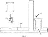
- an electron beam detecting device may include an electron collecting scaffold 106, an electron collecting device, and a first driving device.
- the electron collecting device 101 may be movably installed on the electron collecting scaffold 106.
- the electron collecting device may be arranged for moving along the electron collecting scaffold 106 as driven by a driving force.
- the first driving device may be connected to the electron collecting device 101.
- the first driving device may be arranged for providing the electron collecting device 101 with the driving force required to move.
- the electron collecting scaffold 106 in the electron beam detecting device may be movably installed to the electron collecting device 101.
- the electron collecting device may be able to move along the electron collecting scaffold 106.
- electrons may be collected at different locations of the electron collecting scaffold 106. Therefore, the degree of uniformity and / or the strength of radiation of the beam of electrons may be gathered.
- the electron collecting device 101 may be mobile with respect to the electron collecting scaffold 106, the electron collecting device may be able to detect beams of electrons at different locations, thereby reducing the number of electron collecting devices 101, lowering hardware cost.
- the electron collecting device 101 may include but is not limited to a Faraday cup, an Aluminum rod, etc.
- the first driving device may be an electric drive, a hydraulic drive, or a pneumatic drive.
- the electric drive may include various types of electric motors, such as a stepper motor, a linear motor, etc.
- the electron collecting scaffold 106 may provide the installation location the electron collecting device 101.
- the electron collecting scaffold may define the range in which the electron collecting device 101 may move.
- the electron collecting scaffold may include an electron collecting rail 107.
- the electron collecting device 101 may be hung over the electron collecting rail 107.
- the electron collecting rail 107 may include a rail groove.
- the electron collecting device 101 may move on the rail groove.
- the electron collecting rail 107 may be a rail pole.
- the electron collecting device 101 may move while covering the rail pole like a sleeve.
- the electron collecting scaffold 106 may be a cross or a rectangular ring scaffold.
- the electron collecting device 101 may move in two dimensions where electrons are to be collected. The two dimensions may be perpendicular to each other, or may form a bevel.
- the electron collecting scaffold 106 may include an electron collecting rail 107.
- the electron collecting device 101 may be movably installed on the electron collecting rail 107.
- the electron collecting device may be allowed at least of a one-dimensional movement along the electron collecting rail 107.
- the electron collecting scaffold 106 may be provided with the electron collecting rail 107 dedicated to movement of the electron collecting device 101.
- the electron collecting device 101 may perform two-dimensional movement, three-dimensional movement or one-dimensional movement.
- the electron collecting device 101 may move in the direction x and the direction y in a plane.
- the direction x may be perpendicular to the direction y.
- such movement may be two-dimensional.
- the electron collecting device 101 may move in three-dimensional space, specifically in the direction x, the direction y, and the direction z. Any two of the direction x, the direction y, and the direction z may be perpendicular to each other.
- the electron collecting device 101 may be provided with the electron collecting rail 107 for the electron collecting device 101 to perform one-dimensional movement.
- the electron collecting rail 107 may be a rectilinear rail.
- the rectilinear rail may specifically include a rectilinear groove, a rectilinear guide pole, etc.
- the electron collecting scaffold 106 may be a movable scaffold.
- the electron collecting device 101 may be allowed to move within the first region.
- the electron collecting device 101 may be allowed to move within the second region.
- the electron collecting scaffold 106 per se may also be a movable scaffold that may be allowed to move with respect to its installation location.
- the movable scaffold may be able to perform linear movement or rotation.
- the movable scaffold may be a rotating scaffold that may rotate.
- the movable scaffold When being located at the first location and the second location with respect to its installation location, the movable scaffold may drag the electron collecting device 101 to get in and get out of the first region.
- the electron collecting device 101 can perform only simple one-dimensional movement, the movement of the movable scaffold per se may allow the electron collecting device 101 to perform multidimensional movement in space.
- the first region may be a processing region where an irradiated product is to be processed.
- the first region may be the region other than the processing region.
- the first region may be the processing region where irradiation processing is to be performed on a product.
- the electron collecting device 101 may avoid interfering with the ongoing irradiation processing.
- the electron collecting device may enter the first region to perform normal detection of the beam of electrons for irradiation.
- the L-shaped movable scaffold may include a first scaffold body.
- the first scaffold body may include a secured end and a free end opposite to the secured end.
- the secured end may be secured on the installation location.
- the L-shaped movable scaffold may include a second scaffold body.
- the second scaffold body may be connected to the free end of the first scaffold body.
- the second scaffold body may be movably connected to the electron collecting device 101.
- the movable scaffold may be an L-shaped rotating right angle.
- the movable scaffold may have a free end and a secured end.
- the secured end may serve to be secured on the installation location of the movable scaffold.
- the free end may rotate around the secured end.
- the movable scaffold may be L-shaped.
- the movable scaffold may be a first scaffold and a second scaffold.
- the first scaffold and the second scaffold may form a right angle of 90 degrees or an angle of nearly 90 degrees.
- the movable scaffold may take up less space in one dimension, facilitating flexible layout of equipment in a factory.
- the movable scaffold may consist of two scaffolds forming a right angle, such that the electron collecting device 101 may access the first region flexibly and easily while reducing the overall rotating angle of the movable scaffold, reducing the large space required by the large rotating angle, again facilitating flexible layout of the factory.
- the movable scaffold may switch from being in the first location to being in the second location.
- the movable scaffold may rotate 90 degrees about the secured end where the movable scaffold is installed.
- the system may further include a second driving device.
- the second driving device may be connected to the movable scaffold.
- the second driving device may be arranged for providing a driving force for moving the movable scaffold.
- the second driving device may drive the movable scaffold to rotate.
- the second driving device may as well be an electric drive or a hydraulic drive.
- the electron collecting device 101 may be located, together with the electron accelerator, inside a shield room.
- the electron collecting device may be arranged for acquiring a first signal by detecting a strength of the beam of electrons radiated by the electron accelerator.
- the sampling box may be located inside the shield room.
- the sampling box may be connected to the electron collecting device 101.
- the sampling box may be arranged for receiving the first signal and converting the first signal into a second signal.
- the second signal may be an optical signal that reflects a degree of uniformity of irradiation of the beam of electrons.
- the communicating box 103 may be located outside the shield room.
- the communicating box may be connected to the sampling box through an optical fiber 105.
- the communicating box may be arranged for receiving the second signal through the optical fiber 105, and converting the second signal into a third signal which is an electric signal.
- the controller 104 may be located outside the shield room.
- the controller may be connected to the communicating box 103.
- the controller may be arranged for receiving the third signal and controlling detection of the beam of electrons.
- the electron beam detecting device may apply to high current irradiation processing.
- the electron collecting device 101 may include but is not limited to a Faraday cup, an Aluminum rod, etc.
- a hollow cavity may be provided inside the electron collecting device 101. With the hollow cavity, the amount of incident charged particles may be detected, thereby detecting the strength of the beam of electrons at a single point in time.
- the first signal may be proportional to the number of electrons incident onto the electron collecting device 101 at a single time point.
- a shield room may be introduced in the electron beam detecting device. Both the electron collecting device 101 and the sampling box may be provided inside the shield room.
- the large current generated by the beam of electrons of high current may be isolated inside the isolating room, reducing risk of breakdown of air by the large current or failure of the communicating box 103, the controller 104, etc., under interference in an environment of a large depth.
- the sampling box may convert the first signal right away into the second signal that is an optical signal.
- An optical signal may be conducted by broadcast, instead of as an electric signal such as a voltage signal or a current signal, and thereby will not be subject to interference of the beam of electrons of high current.
- the controller 104 per se will not be subject to interference.
- the signal may be subject to less interference during transmission, thereby improving accuracy in detecting the beam of electrons.
- the sampling box may acquire the current sampling signal by sampling the current on the electron collecting device 101 at predetermined intervals.
- the predetermined intervals may include identical intervals of an arbitrary duration. Then, the sampling box will periodically sample the current signal on the electron collecting device 101. If the predetermined intervals include at least two different intervals, then the sampling box may gather the current signal on the electron collecting device 101 in time sequence at predetermined intervals.
- the communicating box 103 may be a photoelectric converting device that converts an optical signal into an electric signal.
- the communicating box 103 and the controller 104 may be integrated equipment. That is, the communicating box 103 and the controller 104 may be located in one housing and belong to one piece of physical equipment, such as a server capable of transceiving an optical signal, etc.
- the communicating box 103 and the controller 104 may be physical equipment independent of each other.
- Interference of the beam of electrons of a large current on the detected signal may be reduced by using an isolating room and transmitting the signal using an optical fiber 105 instead of a cable, thereby improving accuracy in detecting the beam of electrons.
- the communicating box 103 and the controller 104 may be located inside a control room.
- a metal shield wall may be provided between the control room and the shield room.
- a perforation through which the optical fiber 105 is to pass may be provided on the metal shield wall.
- the isolating room may have at least one isolating wall.
- the isolating wall may have the communicating box 103 and outside the control room.
- the isolating room may have one or more isolating walls.
- the isolating room may have 2 to 4 isolating walls.
- the isolating wall may be provided with a metal board, metal powder, etc., that forms a metal shield layer.
- an electric signal may be guided into the ground by the metal.
- the alternating electromagnetic field generated by the beam of electrons of alternating high current may further be isolated inside the isolating room by a metal isolating layer, reducing interference of such alternating electromagnetic field on the communicating box 103 and / or the controller 104 inside the control room.
- the sampling box may include a current to voltage converting circuit, a digital to analog converter, a sampling chip, and a photoelectric converting circuit.
- the current to voltage converting circuit may be connected to the electron collecting device 101.
- the current to voltage converting circuit may be arranged for receiving the first signal, which may be a current signal.
- the current to voltage converting circuit may be arranged for converting the current signal into a voltage signal.
- the digital to analog converter may be connected to the current to voltage converting circuit.
- the digital to analog converter may be arranged for converting the voltage signal, which may be an analog signal, into a digital signal.
- the sampling chip may be connected to the digital to analog converter.
- the sampling chip may be arranged for converting the digital signal into a third signal that reflects the degree of uniformity of irradiation of the beam of electrons.
- the photoelectric converting circuit may be connected to the sampling chip.
- the photoelectric converting circuit may be arranged for converting the third signal into the second signal which may be the optical signal.
- the current to voltage converting circuit may be connected to the electron collecting device 101.
- the current to voltage converting circuit naturally will guide, into the sampling box, the current formed while the electron collecting device 101 accepts radiation of the beam of electrons intruding onto the electron collecting device 101.
- the current to voltage converting circuit may convert the current signal into the voltage signal of a value corresponding to the value of the current signal.
- the voltage signal may be referred to as so to distinguish it from another voltage signal.
- the "first" in the name of the voltage signal may not have any material meaning.
- the first signal may refer in general to the current signal received by the current to voltage converting circuit from the electron collecting device 101.
- the voltage signal formed by the current to voltage converting circuit may be an analog signal.
- the sampling box may further include a digital to analog converter.
- the digital to analog converter may acquire the digital signal by discretization of the analog signal.
- the sampling chip on one hand may control the signal sampling by the sampling box, and on the other hand may control the signal conversion by the sampling box.
- the sampling chip may include a programmable array.
- the programmable circuit may include but is not limited to a Field-Programmable Gate Array (FPGA) and / or a complex programmable array.
- FPGA Field-Programmable Gate Array
- the sampling chip may further include a microprocessor or an Application Specific Integrated Circuit (ASIC).
- the sampling chip may be a microcontroller 104 or a micro controlling circuit of various forms located in the sampling box.
- the sampling chip may convert, through signal conditioning, the strength of the signal at a single point in time into the strength of the signal containing multiple single points for comparison, conversion, etc., to acquire the degree of uniformity of irradiation of the beam of electrons within the period of the signal of the multiple single points.
- the sampling chip may further serve to amplify a signal, filter an interfering signal, etc. By signal amplification, a weak signal may be converted into a strong signal, thereby reducing signal loss due to attenuation, etc., during transmission.
- the sampling chip may also filter an interfering signal.
- the interfering signal may be filtered out through difference in the signal frequency, thereby improving the signal to noise ratio of the signal, again improving accuracy of a subsequent result detected.
- the sampling box may further include a photoelectric converting circuit.
- the sampling chip may acquire, using the digital signal gathered at a single time point, the third signal that measures the degree of uniformity of irradiation of the beam of electrons within a period of time.
- the third signal may be a signal such as a voltage pulse.
- the photoelectric converting circuit will convert the received electric signal into an optical signal.
- the optical signal may be referred to as the second electric signal.
- the second electric signal may be transmitted to the communicating box 103 via the optical fiber 105.
- the optical fiber 105 may include but is not limited to a single mode optical fiber 105 or a multimode optical fiber 105. There may be one or more optical fibers 105. The bandwidth of the optical fiber 105 may be provided as demanded by the amount of data to be transmitted.
- the electron collecting scaffold 106 may be movably installed on an irradiation processing production line. Such movable installation may allow the electron collecting scaffold 106 to move on the irradiation processing production line. For example, the electron collecting scaffold 106 may be moved, such that the electron collecting device 101 is moved from the location A to the location B. The electron collecting device 101 may be driven by the electron collecting scaffold 106 to get in and get out of the processing location where a product is to be processed. If the electron collecting device 101 has entered the processing location, then the electron collecting device instead of the product being processed may experience irradiation of the beam of electrons. If the electron collecting device has left the processing location, then the processing location becomes available, so that a product to be processed may be placed there and irradiation processing may continue.
- the electron collecting scaffold 106 may be, but is not limited to, a mechanical arm capable of carrying the electron collecting device 101 to move.
- an electron beamline focusing device for irradiation processing industry may contain three sets of permanent magnets.
- the four magnets 1 to 4 of the first set of permanent magnets may be secured onto the yoke I.
- the yoke I may be secured on the rail, and may serve to focus the incident beamline in the transverse direction X.
- the four magnetic poles 5 ⁇ 8 of the second set of permanent magnets may be secured onto the yoke II.
- the yoke II may adjust the location of the set of magnets back and forth using adjusting screws 13 to 16 and by cooperating with the rails inserted in the through holes 17 to 20, to focus the incident beamline in the transverse direction Y.
- the four magnetic poles 9 ⁇ 12 of the third set of permanent magnets may be secured onto the yoke III.
- the yoke III may adjust the location of the quadrupole magnets back and forth using adjusting screws 13 ⁇ 16 and by cooperating with the rails inserted in the through holes 17 ⁇ 20.
- the length of the drift space of the restrained beam may be altered by adjusting the locations of the second set of permanent magnets and the third set of permanent magnets. Beams of electrons restrained with different parameters may be focused by combining drift spaces of different lengths and the locations of the permanent magnets.
- FIG. 7 is the change in the parameter ⁇ of the device when the restrained beam of electrons of energy of emittance passes through the device according to the example.
- the parameter ⁇ may be the envelope of the amplitude of the restrained beam during transmission.
- the parameter may reflect focus performance of the beamline. It may be seen that with the example, the restrained beam may be focused in both the transverse directions X and Y by combining three sets of permanent magnets and the drift spaces.
- the horizontal axis may be the length of space (in units of m) in which the beam of electrons drift; and the vertical axis may be the parameter ⁇ of the drifting beam of electrons.
- the parameter ⁇ in the direction X may be ⁇ x .
- the parameter ⁇ in the direction Y may be ⁇ y . It may be seen in FIG. 7 that values of the parameter ⁇ in both the direction X and the direction Y are small, achieving ideal beam restraining effect (i.e., focusing effect).
- the system of electron irradiation may further include an electron beam detecting device arranged for detecting the beam of electrons.
- the electron beam detecting device may include an electron collecting device, a sampling box, a communicating box, and a controller.
- the electron collecting device 101 may be located, together with the electron accelerator, inside a shield room.
- the electron collecting device may be arranged for acquiring a first signal by detecting a strength of the beam of electrons radiated by the electron accelerator.
- the sampling box 102 may be located inside the shield room.
- the sampling box may be connected to the electron collecting device 101.
- the sampling box may be arranged for receiving the first signal and converting the first signal into a second signal.
- the second signal may be an optical signal that reflects a degree of uniformity of irradiation of the beam of electrons.
- the communicating box 103 may be located outside the shield room.
- the communicating box may be connected to the sampling box 102 through an optical fiber 105.
- the communicating box may be arranged for receiving the second signal through the optical fiber 105, and converting the second signal into a third signal which is an electric signal.
- the controller 104 may be located outside the shield room.
- the controller may be connected to the communicating box 103.
- the controller may be arranged for receiving the third signal and controlling detection of the beam of electrons.
- the electron beam detecting device may apply to high current irradiation processing.
- the electron collecting device 101 may include but is not limited to a Faraday cup, an Aluminum rod, etc.
- a hollow cavity may be provided inside the electron collecting device 101. With the hollow cavity, the amount of incident charged particles may be detected, thereby detecting the strength of the beam of electrons at a single point in time.
- the first signal may be proportional to the number of electrons incident onto the electron collecting device 101 at a single time point.
- a shield room may be introduced in the electron beam detecting device. Both the electron collecting device 101 and the sampling box 102 may be provided inside the shield room.
- the large current generated by the beam of electrons of high current may be isolated inside the isolating room, reducing risk of breakdown of air by the large current or failure of the communicating box 103, the controller 104, etc., under interference in an environment of a large depth.
- the sampling box 102 may convert the first signal right away into the second signal that is an optical signal.
- An optical signal may be conducted by broadcast, instead of as an electric signal such as a voltage signal or a current signal, and thereby will not be subject to interference of the beam of electrons of high current.
- the controller 104 per se will not be subject to interference.
- the signal may be subject to less interference during transmission, thereby improving accuracy in detecting the beam of electrons.
- the sampling box 102 may acquire the current sampling signal by sampling the current on the electron collecting device 101 at predetermined intervals.
- the predetermined intervals may include identical intervals of an arbitrary duration. Then, the sampling box 102 will periodically sample the current signal on the electron collecting device 101. If the predetermined intervals include at least two different intervals, then the sampling box 102 may gather the current signal on the electron collecting device 101 in time sequence at predetermined intervals.
- the communicating box 103 may be a photoelectric converting device that converts an optical signal into an electric signal.
- the communicating box 103 and the controller 104 may be integrated equipment. That is, the communicating box 103 and the controller 104 may be located in one housing and belong to one piece of physical equipment, such as a server capable of transceiving an optical signal, etc.
- the communicating box 103 and the controller 104 may be physical equipment independent of each other.
- Interference of the beam of electrons of a large current on the detected signal may be reduced by using an isolating room and transmitting the signal using an optical fiber 105 instead of a cable, thereby improving accuracy in detecting the beam of electrons.
- the communicating box 103 and the controller 104 may be located inside a control room.
- a metal shield wall may be provided between the control room and the shield room.
- a perforation through which the optical fiber 105 is to pass may be provided on the metal shield wall.
- the isolating room may have at least one isolating wall.
- the isolating wall may isolate the communicating box 103 to the control room.
- the isolating room may have one or more isolating walls.
- the isolating room may have 2 to 4 isolating walls.
- the isolating wall may be provided with a metal board, metal powder, etc., that forms a metal shield layer.
- an electric signal may be guided into the ground by the metal.
- the alternating electromagnetic field generated by the beam of electrons of alternating high current may further be isolated inside the isolating room by a metal isolating layer, reducing interference of such alternating electromagnetic field on the communicating box 103 and / or the controller 104 inside the control room.
- the sampling box 102 may include a current to voltage converting circuit, a digital to analog converter, a sampling chip, and a photoelectric converting circuit.
- the current to voltage converting circuit may be connected to the electron collecting device 101.
- the current to voltage converting circuit may be arranged for receiving the first signal, which may be a current signal.
- the current to voltage converting circuit may be arranged for converting the current signal into a voltage signal.
- the digital to analog converter may be connected to the current to voltage converting circuit.
- the digital to analog converter may be arranged for converting the voltage signal, which may be an analog signal, into a digital signal.
- the sampling chip may be connected to the digital to analog converter.
- the sampling chip may be arranged for converting the digital signal into a third signal that reflects the degree of uniformity of irradiation of the beam of electrons.
- the photoelectric converting circuit may be connected to the sampling chip.
- the photoelectric converting circuit may be arranged for converting the third signal into the second signal which may be the optical signal.
- the current to voltage converting circuit may be connected to the electron collecting device 101.
- the current to voltage converting circuit naturally will guide, into the sampling box 102, the current formed while the electron collecting device 101 accepts radiation of the beam of electrons intruding onto the electron collecting device 101.
- the current to voltage converting circuit may convert the current signal into the voltage signal of a value corresponding to the value of the current signal.
- the voltage signal may be referred to as so to distinguish it from another voltage signal.
- the "first" in the name of the voltage signal may not have any material meaning.
- the first signal may refer in general to the current signal received by the current to voltage converting circuit from the electron collecting device 101.
- the voltage signal formed by the current to voltage converting circuit may be an analog signal.
- the sampling box 102 may further include a digital to analog converter.
- the digital to analog converter may acquire the digital signal by discretization of the analog signal.
- the sampling chip on one hand may control the signal sampling by the sampling box 102, and on the other hand may control the signal conversion by the sampling box 102.
- the sampling chip may include a programmable array.
- the programmable circuit may include but is not limited to a Field-Programmable Gate Array (FPGA) and / or a complex programmable array.
- FPGA Field-Programmable Gate Array
- the sampling chip may further include a microprocessor or an Application Specific Integrated Circuit (ASIC).
- the sampling chip may be a microcontroller 104 or a micro controlling circuit of various forms located in the sampling box 102.
- the sampling chip may convert, through signal conditioning, the strength of the signal at a single point in time into the strength of the signal containing multiple single points for comparison, conversion, etc., to acquire the degree of uniformity of irradiation of the beam of electrons within the period of the signal of the multiple single points.
- the sampling chip may further serve to amplify a signal, filter an interfering signal, etc. By signal amplification, a weak signal may be converted into a strong signal, thereby reducing signal loss due to attenuation, etc., during transmission.
- the sampling chip may also filter an interfering signal.
- the interfering signal may be filtered out through difference in the signal frequency, thereby improving the signal to noise ratio of the signal, again improving accuracy of a subsequent result detected.
- the sampling box 102 may further include a photoelectric converting circuit.
- the sampling chip may acquire, using the digital signal gathered at a single time point, the third signal that measures the degree of uniformity of irradiation of the beam of electrons within a period of time.
- the third signal may be a signal such as a voltage pulse.
- the photoelectric converting circuit will convert the received electric signal into an optical signal.
- the optical signal may be referred to as the second electric signal.
- the second electric signal may be transmitted to the communicating box 103 via the optical fiber 105.
- the optical fiber 105 may include but is not limited to a single mode optical fiber 105 or a multimode optical fiber 105. There may be one or more optical fibers 105. The bandwidth of the optical fiber 105 may be provided as demanded by the amount of data to be transmitted.
- the system of electron irradiation may further include an electron collecting scaffold and a driving device.
- the driving device may be connected to the electron collecting device 101.
- the driving device may be arranged for providing the electron collecting device 101 with a driving force.
- the electron collecting device 101 may be installed on the electron collecting scaffold 106. Driven by the driving force, the electron collecting device may move based on the electron collecting scaffold 106.
- the system may include an electron collecting scaffold 106.
- the electron collecting device 101 may be installed on the electron collecting scaffold.
- the electron collecting device 101 may move driven by the driving force provided by the driving device. This is equivalent to providing multiple electron collecting devices 101 at different locations of the electron collecting scaffold 106.
- one mobile electron collecting device 101 instead of multiple electron collecting devices 101 may collect the strength of irradiation of the beam of electrons at different locations, thereby reducing the number of electron collecting devices 101, lowering hardware cost of the system.
- the electron collecting scaffold 106 may be a cross or a rectangular ring scaffold.
- the electron collecting device 101 may move in two dimensions where electrons are to be collected. The two dimensions may be perpendicular to each other, or may form a bevel.
- the electron collecting scaffold 106 may include an electron collecting rail 107.
- the electron collecting device 101 may be movably installed on the electron collecting rail 107.
- the electron collecting device may be allowed of a one-dimensional movement along the electron collecting rail 107.
- the electron collecting scaffold may include an electron collecting rail 107.
- the electron collecting device 101 may be hung over the electron collecting rail 107.
- the electron collecting rail 107 may include a rail groove.
- the electron collecting device 101 may move on the rail groove.
- the electron collecting rail 107 may be a rail pole.
- the electron collecting device 101 may move while covering the rail pole like a sleeve.
- the driving device may include a stepper motor.
- the driving device may be an electric driving device, a hydraulic driving device, a pneumatic driving device, etc.
- the driving device may be an electric driving device and a stepper motor.
- the stepper motor may be of a simple structure and low hardware cost.
- the electron collecting scaffold 106 may be movably installed on an installation location of an irradiation processing production line.
- the electron collecting device 101 may be located on a processing location of the irradiation processing production line, and may be arranged for detecting the strength of the beam of electrons for irradiation processing.
- a product may be processed at the processing location.
- the electron collecting device 101 may be located off the processing location.
- the electron collecting scaffold 106 may be movably installed on an irradiation processing production line. Such movable installation may allow the electron collecting scaffold 106 to move on the irradiation processing production line. For example, the electron collecting scaffold 106 may be moved, such that the electron collecting device 101 is moved from the location A to the location B. The electron collecting device 101 may be driven by the electron collecting scaffold 106 to get in and get out of the processing location where a product is to be processed. If the electron collecting device 101 has entered the processing location, then the electron collecting device instead of the product being processed may experience irradiation of the beam of electrons. If the electron collecting device has left the processing location, then the processing location becomes available, so that a product to be processed may be placed there and irradiation processing may continue.
- the electron collecting scaffold 106 may be, but is not limited to, a mechanical arm capable of carrying the electron collecting device 101 to move.
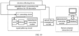
- the electron collecting device may be installed on an adjustable bench cooperating with the electron collecting rail on the electron collecting scaffold in one-dimensional movement.
- the gathering box may include an I-V converting circuit (which may correspond to the current to voltage converting circuit), a digital to analog converter (A/D), a Field-Programmable Gate Array (FPGA), and a photoelectric converting module, composing the signal sampling circuit in the sampling box.
- the signal sampling circuit may exchange data with the human-computer interaction end (corresponding to the controller) inside the control room through the optical fiber communication link formed by the optical fiber. For example, data transmitted through the optical fiber communication link may be converted into an electric signal through the photoelectric converting module. The electric signal may then be stored in a database.
- the structure of the device for detecting online the degree of uniformity of irradiation of a strong beam of electrons of high current may mainly include an electron collecting platform, a local sampling box, a communicating box, a human-computer interaction end, and a related connecting optical fiber.
- the electron collecting platform and the local sampling box may be placed inside the shield room.
- the other components may be placed in the control room.
- the components in the two room may be connected by the optical fiber passing through the wall.
- the degree of uniformity of irradiation of a strong beam of electrons of high current may be detected online as follows.
- the device may include an electron collecting device, which may convert a restrained beam into an electric signal.
- the device may include an adjustable bench for one-dimensional movement, which may control the location of the probe to control movement of online measurement.
- the device may include a signal gathering circuit, which may process, such as amplify, filter, etc., the signal of the probe.
- the device may include an optical fiber communication link, which may isolate the high voltage of the beam restraining section and transmit the measurement signal.
- the device may include a human-computer interaction end, which may provide a convenient human-computer interaction interface, facilitate controlling the gathering process, and acquire measurement data.
- the system may employ the adjustable bench for one-dimensional movement as shown in FIG. 11 to FIG. 14 .
- the electron collecting device may be secured on the one dimensional rail by screw.
- the rail may move back and forth in one direction under control of the stepper motor.
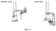
- the bench for one-dimensional movement may be secured on the flip scaffold.
- the flip scaffold may be connected to the scanning box through a motor of a large torque.
- the flip scaffold may be flipped by controlling the steering gear. During normal operation, the entire device may be flipped beside the scanning box. when measurement is required, the steering gear may be controlled remotely to flip the device to place it under the scanning box.
- the flip scaffold (a movable scaffold) may flip the electron collecting device to place it on the processing location of the irradiation production line.
- the processing location may be where a product is to be irradiated.
- the flip scaffold may flip the electron collecting device to withdraw it from the processing location where a product is to be irradiated, to allow normal irradiation processing.
- an electron beam detecting device may include an accelerator scanning box, a flip scaffold, a steering gear of a large torque, a one dimensional rail, an electron collecting device, and a stepper motor.
- the accelerator scanning may be arranged for accelerating a beam of electrons.
- the steering gear of a large torque may be connected to the flip scaffold.
- the steering gear may be arranged for providing the driving force that drives the flip scaffold to flip.
- the one dimensional rail may be an electron collecting rail provided on the flip scaffold.
- the one dimensional rail may serve for one dimensional linear movement of the electron collecting device along the one dimensional rail.
- the electron collecting device may be movably installed on the one dimensional rail.
- the stepper motor may be a driving device for driving the electron collecting device.
- the stepper motor may convert electric energy into mechanical energy by rotating a motor per se, and drive the electron collecting device.
- the disclosed equipment and method may be implemented in other ways.
- the described equipment embodiments are merely exemplary.
- the unit division is merely logical function division and can be other division in actual implementation.
- multiple units or components can be combined, or integrated into another system, or some features/characteristics can be omitted or skipped.
- the coupling, or direct coupling or communicational connection among the components illustrated or discussed herein may be implemented through indirect coupling or communicational connection among some interfaces, equipment, or units, and may be electrical, mechanical, or in other forms.
- the units described as separate components may or may not be physically separated.
- Components shown as units may be or may not be physical units; they may be located in one place, or distributed on multiple network units. Some or all of the units may be selected to achieve the purpose of a solution of the embodiments as needed.
- functional units in embodiments herein may all be integrated in one processing unit, or exist as separate units respectively; or two or more such units may be integrated in one unit.
- the integrated unit may be implemented in form of hardware, or hardware plus software functional unit(s).
- the computer-readable storage medium may be various media that can store program codes, such as mobile storage equipment, Read Only Memory (ROM), Random Access Memory (RAM), a magnetic disk, a CD, and/or the like.
Landscapes
- Physics & Mathematics (AREA)
- Spectroscopy & Molecular Physics (AREA)
- Engineering & Computer Science (AREA)
- General Physics & Mathematics (AREA)
- Plasma & Fusion (AREA)
- Health & Medical Sciences (AREA)
- Life Sciences & Earth Sciences (AREA)
- High Energy & Nuclear Physics (AREA)
- Molecular Biology (AREA)
- Optics & Photonics (AREA)
- Electromagnetism (AREA)
- Power Engineering (AREA)
- Particle Accelerators (AREA)
- Electron Sources, Ion Sources (AREA)
- Analysing Materials By The Use Of Radiation (AREA)
Abstract
Description
- This application is based on, and claims benefit of priority to, Chinese Application No.
201910239420.8 201910239421.2 201910239390.0 201910239970.X - The subject disclosure relates, but is not limited, to field of irradiation processing, and in particular to an electron beam focusing device.
- There may be two types of sources of radiation for radiation processing. One may be a source of a radioactive isotope such as cobalt. The other may be an accelerator for accelerating charged particles such as electrons. An electron accelerator is advantageous as follows. Energy is controllable. A beam of electrons may essentially act on a product illuminated by the beam with high utilization. There is no issue of processing a source of radioactive waste. No electricity is consumed during shutdown. There is barely any pollution to the environment during the entire production except for a trace of ozone being produced. Consequently, more users tend to employ an electron accelerator in radiation processing.
- During transmission of a beam of electrons accelerated in an electron accelerator, the greater a transverse envelope and a longitudinal envelope of the beam are, the greater a beam restraining loss, and the poorer the transmission performance of the beam restraining. In some cases, once production of an electron beam focusing device completes, then a performance parameter for the device to perform beam restraining on a beam of electrons is determined, failing to meet demands of focusing a beam of electrons in different application scenes.
- In view of this, at least one embodiment herein provides a system of electron irradiation.
- A system of electron irradiation includes an electron accelerator and an electron beam focusing device.
- The electron accelerator is arranged for emitting and accelerating a beam of electrons.
- The electron beam focusing device is located at a rear end of the electron irradiation. The electron beam focusing device includes a beam restraining rail and 2n+1 sets of magnetic poles.
- The beam restraining rail forms a beam restraining channel through which the beam of electrons are to pass.
- The 2n+1 sets of magnetic poles are installed on the beam restraining rail. The 2n+1 sets of magnetic poles are distributed at different locations of the beam restraining channel. An nth set of magnetic poles of the 2n+1 sets of magnetic poles are arranged for performing, on the beam of electrons, focusing in a first direction. An (n+1)th set of magnetic poles of the 2n+1 sets of magnetic poles are arranged for performing, on the beam of electrons, focusing in a second direction. The second direction is perpendicular to the first direction. The n is a positive integer.
- The 2n+1 sets of magnetic poles may include a first set of magnetic poles, a second set of magnetic poles, and a third set of magnetic poles.
- The first set of magnetic poles may be arranged for performing, on the beam of electrons, first-time focusing in the first direction.
- The second set of magnetic poles may be arranged for performing, on the beam of electrons, focusing in the second direction.
- The third set of magnetic poles may be arranged for performing, on the beam of electrons, second-time focusing in the first direction.
- At least part of the 2n+1 sets of magnetic poles may be movably installed on the beam restraining rail, with a spacing between any two neighbor sets of magnetic poles being adjustable.
- Of the 2n+1 sets of magnetic poles, a second set of magnetic poles and / or a third set of magnetic poles may be movably installed on the beam restraining rail.
- Different locations of the second set of magnetic poles on the beam restraining rail may correspond respectively to different first spacings between the second set of magnetic poles and a first set of magnetic poles of the 2n+1 sets of magnetic poles.
- And / or, different locations of the third set of magnetic poles on the beam restraining rail may correspond respectively to different second spacings between the third set of magnetic poles and the second set of magnetic poles.
- Different spacings between a first set of magnetic poles and a last set of magnetic poles of the 2n+1 sets of magnetic poles may correspond respectively to different lengths of a drift space in the beam restraining channel in which the beam of electrons drift.
- The sets of magnetic poles may be sets of quadrupole magnetic poles.
- The sets of quadrupole magnetic poles may be composed of permanent magnets.
- The permanent magnets may be made from NdFeB.
- A permanent magnet of the 2n+1 sets of magnetic poles may be installed on the beam restraining rail through a yoke ring.
- The yoke ring may be made by connecting multiple yokes. Different connection locations between two neighbor yokes may correspond respectively to different diameters of the yoke ring.
- The system may further include an electron beam detecting device arranged for detecting the beam of electrons.
- The electron beam detecting device may include an electron collecting device, a sampling box, a communicating box, and a controller.
- The electron collecting device may be located, together with the electron accelerator, inside a shield room. The electron collecting device may be arranged for acquiring a first signal by detecting a strength of the beam of electrons radiated by the electron accelerator.
- The sampling box may be located inside the shield room. The sampling box may be connected to the electron collecting device. The sampling box may be arranged for receiving the first signal and converting the first signal into a second signal which is an optical signal that reflects a degree of uniformity of irradiation of the beam of electrons.
- The communicating box may be located outside the shield room. The communicating box may be connected to the sampling box through an optical fiber. The communicating box may be arranged for receiving the second signal through the optical fiber and converting the second signal into a third signal which is an electric signal.
- The controller may be located outside the shield room. The controller may be connected to the communicating box. The controller may be arranged for receiving the third signal and controlling detection of the beam of electrons.
- The communicating box and the controller may be located inside a control room. A metal shield wall may be provided between the control room and the shield room.
- A perforation through which the optical fiber is to pass may be provided on the metal shield wall.
- The sampling box may include a current to voltage converting circuit, a digital to analog converter, a sampling chip, and a photoelectric converting circuit.
- The current to voltage converting circuit may be connected to the electron collecting device. The current to voltage converting circuit may be arranged for receiving the first signal, which is a current signal, and converting the current signal into a voltage signal.
- The digital to analog converter may be connected to the current to voltage converting circuit. The digital to analog converter may be arranged for converting the voltage signal, which may be an analog signal, into a digital signal.
- The sampling chip may be connected to the digital to analog converter. The sampling chip may be arranged for converting the digital signal into a third signal that reflects the degree of uniformity of irradiation of the beam of electrons,
- The photoelectric converting circuit may be connected to the sampling chip. The photoelectric converting circuit may be arranged for converting the third signal into the second signal which is the optical signal.
- The system may further include an electron collecting scaffold and a driving device.
- The driving device may be connected to the electron collecting device.
- The driving device may be arranged for providing the electron collecting device with a driving force.
- The electron collecting device may be installed on the electron collecting scaffold. Driven by the driving force, the electron collecting device may move based on the electron collecting scaffold.
- The electron collecting scaffold may include an electron collecting rail.
- The electron collecting device may be movably installed on the electron collecting rail. The electron collecting device may be allowed of a one-dimensional movement along the electron collecting rail.
- The driving device may include a stepper motor.
- The electron collecting scaffold may be movably installed on an installation location of an irradiation processing production line.
- If the electron collecting scaffold is located at a first location, the electron collecting device may be located on a processing location of the irradiation processing production line, and may be arranged for detecting the strength of the beam of electrons for irradiation processing. The processing location may be where a product is to be processed.
- If the electron collecting scaffold is located at a second location, the electron collecting device may be located off the processing location.
- With an electron beam focusing device according to at least one embodiment herein, an odd number of sets of magnetic poles may be installed on a beam restraining rail. Any set of magnetic poles of an odd ordinal number may focus the beam of electrons in a direction different from a direction in which any set of magnetic poles of an even ordinal number may focus the beam of electrons. As there may be an odd total number of sets of magnetic poles, a subsequent set of magnetic poles may focus the beam of electrons again to at least partially cancel out defocusing effect in the focusing direction of the set of magnetic poles under consideration brought about by a prior set of magnetic poles, thereby improving focusing effect of the electron beam focusing device, ultimately improving focus performance of the beam of electrons.
-
-
FIG. 1 is a diagram of a structure of a system of electron irradiation according to an embodiment herein. -
FIG. 2 is a diagram of a 3D structure of an electron beam focusing device according to an embodiment herein. -
FIG. 3 is a diagram of a side structure of the electron beam focusing device according to an embodiment herein. -
FIG. 4 to FIG. 6 are a diagram of a structure of the electron beam focusing device shown inFIG. 3 , in a D-D section. -
FIG. 7 is a diagram of effect of a parameter β of an electron beam focusing device according to an embodiment herein. -
FIG. 8 is a diagram of a structure of an electron beam detecting device according to an embodiment herein. -
FIG. 9 is a diagram of a structure of an electron beam detecting device according to an embodiment herein. -
FIG. 10 is a diagram of a structure of an electron beam detecting device according to an embodiment herein. -
FIG. 11 is a diagram of structures of an electron collecting device and an electron collecting scaffold according to an embodiment herein. -
FIG. 12 is a diagram of structures of an electron collecting device and an electron collecting scaffold according to an embodiment herein. -
FIG. 13 is a diagram of structures of an electron collecting device and an electron collecting scaffold according to an embodiment herein. -
FIG. 14 is a diagram of structures of an electron collecting device and an electron collecting scaffold according to an embodiment herein. - A technical solution of the subject disclosure is further elaborated below with reference to the drawings and embodiments.
- As shown in
FIG. 1 , according to an embodiment, a system of electron irradiation may include an electron accelerator and an electron beam focusing device. - The electron accelerator may be arranged for emitting and accelerating a beam of electrons.
- The electron beam focusing device may be located at a rear end of the electron irradiation. The electron beam focusing device may include a beam restraining rail and 2n+1 sets of magnetic poles.
- The beam restraining rail may form a beam restraining channel through which the beam of electrons are to pass.
- The 2n+1 sets of magnetic poles may be installed on the beam restraining rail. The 2n+1 sets of magnetic poles may be distributed at different locations of the beam restraining channel. An nth set of magnetic poles of the 2n+1 sets of magnetic poles may be arranged for performing, on the beam of electrons, focusing in a first direction. An (n+1)th set of magnetic poles of the 2n+1 sets of magnetic poles may be arranged for performing, on the beam of electrons, focusing in a second direction. The second direction may be perpendicular to the first direction. The n may be a positive integer.
- A system of electron irradiation may include an accelerator capable of emitting a beam of electrons.
- An electron accelerator may emit and accelerate electrons to form a beam of high-speed electrons. An electron beam focusing device may be located at a rear end of the electron accelerator. The electron beam focusing device may perform, on the beam of electrons through an odd number of sets of magnetic poles, an odd number of focusing operations in different directions, to at least partially cancel out defocusing effect in the focusing direction of the set of magnetic poles under consideration brought about by a prior set of magnetic poles, thereby improving focusing effect of the electron beam focusing device, ultimately improving focus performance of the beam of electrons.
- As shown in
FIG. 2 to FIG. 6 , according to an embodiment, an electron beam focusing device may include a beam restraining rail and 2n+1 sets of magnetic poles. - The beam restraining rail may form a beam restraining channel through which the beam of electrons are to pass.
- The 2n+1 sets of magnetic poles may be installed on the beam restraining rail. The 2n+1 sets of magnetic poles may be distributed at different locations of the beam restraining channel. An nth set of magnetic poles of the 2n+1 sets of magnetic poles may be arranged for performing, on the beam of electrons, focusing in a first direction. An (n+1)th set of magnetic poles of the 2n+1 sets of magnetic poles may be arranged for performing, on the beam of electrons, focusing in a second direction. The second direction may be perpendicular to the first direction. The n may be a positive integer.
- With a structure of the electron beam focusing device according to an embodiment herein, a beam of electrons are focused, avoiding forming of a beam spot of an excessively large area by a beam of unfocused electrons caused by beam defocusing.
- According to an embodiment, an electron beam focusing device may apply to an irradiation processing system. An electron beam focusing device contained in an irradiation processing system may be located at a rear end of an electron accelerator and a front end of a radiation processing device. The electron accelerator may generate a beam of electrons. The beam of electrons may be focused by the beam restraining channel formed by the electron beam focusing device. The beam of electrons may then uniformly reach a product to be processed by the radiation processing device.
- There may be multiple beam restraining rails. The multiple beam restraining rails may be distributed on both sides of the beam restraining channel. The multiple beam restraining rails may be distributed in a direction in which the beam restraining channel extends. In
FIG. 2 , a beam restraining rail may be a column threaded on the surface. The sets of magnetic poles may be secured using nuts at different locations. -
FIG. 2 andFIG. 3 show three sets of magnetic poles. - For example, a beam of electrons may move from a first end of the beam restraining channel towards a second end of the beam restraining channel. Distribution of the beam restraining rails may also extend from the first end towards the second end.
- A beam of electrons may be composed of electrons. An electron per se may be a charged particle.
- The sets of magnetic poles will form a magnetic field. A charged particle moving in a magnetic field will be subject to a magnetic field force. A magnetic field force may be applied to a beam of electrons using 2n+1 sets of magnetic poles. Effect of defocusing of the beam of electrons may be relieved through constraint of the magnetic field force, allowing the beam of electrons to focus.
- A set of magnetic poles may include multiple magnets. The magnets may interact with each other to form a magnetic field that focuses the beam of electrons.
- There may be an odd number of sets of magnetic poles. The odd number of sets of magnetic poles may be distributed at different locations of the beam restraining channel. The sets of magnetic poles may be arranged for performing, on the beam of electrons, focusing in at least two directions. The two directions may be perpendicular to each other.
- For example, of two neighbor sets of magnetic poles, the first set of magnetic poles may perform, on the beam of electrons, focusing in the first direction. The second set of magnetic poles may perform, on the beam of electrons, focusing in the second direction.
- There may be an odd number of sets of magnetic poles. If only 2 sets of magnetic poles were employed in focusing, while focusing the beam of electrons, the second set of magnetic poles would have defocused the beam of electrons in the focusing direction of the first set of magnetic poles. In the embodiment, after being focused by the secondary set in a different direction, the beam of electrons will be focused again, such that impact of focusing the beam of electrons in one direction the other direction may be reduced. Thus, with an electron beam focusing device containing 2n+1 sets of magnetic poles, a beam of electrons may be better focused, and a size of a beam spot of a beam of electrons formed may meet an expected trait in both the first direction and the second direction.
- The n may be an arbitrary positive integer. Specifically, the n may range between 1 and 5. More specifically, the n may range between 1 and 3.
- If the n is 1, then the electron beam focusing device has 3 sets of magnetic poles. The 3 sets of magnetic poles may be spaced at different locations of the beam restraining channel, and each restrain the beam of electrons in a separate direction.
- The mth set of magnetic poles and the (m+2)th set of magnetic poles may focus the beam of electrons in one direction. The m may be a positive integer less than the n. To allow the (m+1)th set of magnetic poles to focus the beam of electrons in the other direction in spite of the (m+2)th set of magnetic poles, the strength of the magnetic field formed by the (m+2)th set of magnetic poles may be weaker than the strength of the magnetic field formed by the mth set of magnetic poles or the (m+1)th set of magnetic poles.
- Of course, the strength of the magnetic field formed by the mth set of magnetic poles may be identical to the strength of the magnetic field formed by the (m+2)th set of magnetic poles. The strength of the magnetic field formed by the mth set of magnetic poles may as well be identical to the strength of the magnetic field formed by the (m+1)th set of magnetic poles.
- The 2n+1 sets of magnetic poles may include a first set of magnetic poles, a second set of magnetic poles, and a third set of magnetic poles.
- The first set of magnetic poles may be arranged for performing, on the beam of electrons, first-time focusing in the first direction.
- The second set of magnetic poles may be arranged for performing, on the beam of electrons, focusing in the second direction.
- The third set of magnetic poles may be arranged for performing, on the beam of electrons, second-time focusing in the first direction.
- The n may equal 1. Then, there may be a total number of 3 sets of magnetic poles, i.e., the first set of magnetic poles, the second set of magnetic poles, and the third set of magnetic poles. The first set of magnetic poles and the third set of magnetic poles may be sets of magnetic poles of odd ordinal numbers, the second set of magnetic poles may be the set of magnetic poles of an even ordinal number. The third set of magnetic poles and the first set of magnetic poles may focus the beam of electrons in one direction, opposite to the direction in which the second magnetic pole may focus the beam of electrons.
- After the first set of magnetic poles have performed, on the beam of electrons, the first-time focusing the first direction, the second set of magnetic poles may focus the beam of electrons in the second direction, which may defocus the beam of electrons in the first direction. To ensure that the beam of electrons is sufficiently focused in the first direction, the third set of magnetic poles may be used to perform, on the beam of electrons, the second-time focusing in the first direction, thereby at least partially cancelling out possible impact of the second set of magnetic poles on the focusing of the beam of electrons in the first direction.
- For example, at least part of the 2n+1 sets of magnetic poles may be movably installed on the beam restraining rail. A spacing between any two neighbor sets of magnetic poles thereon may be adjustable.
- Spacing among all or part of neighbor sets of magnetic poles may be adjustable. Therefore, once the number of the sets of magnetic poles is determined, spacing between the first set of magnetic poles and the last set of magnetic poles may be adjusted by adjusting spacing between two neighbor sets of magnetic poles. Therefore, a drifting space formed by the sets of magnetic poles in which the beam of electrons may drift may be adjustable, thereby meeting a demand for different drifting spaces for the beam of electrons.
- The sets of magnetic poles may be movably installed on the beam restraining rail in at least one mode as follows:
- A set of magnetic poles may be installed on the beam restraining rail through a clamping structure. The clamping structure may be in a first state or a second state. The clamping structure in the first state may secure the set of magnetic poles on the beam restraining rail. There may be at least one free end between the clamping structure in the second state and the beam restraining rail. In this case, the set of magnetic poles and the clamping structure may move, such as slide, on the beam restraining rail as a whole.
- A set of magnetic poles may be movably installed on the beam restraining rail through a screw. Screw holes where the screw is to be screwed on or off may be provided at different locations of the beam restraining rail. The location of the set of magnetic poles on the beam restraining rail may be regulated by engaging the screw with threads of different screw holes, thereby regulating spacing between two neighbor sets of magnetic poles.
- All 2n+1 sets of magnetic poles may be movably installed on the beam restraining rail. The location of any set of magnetic poles on the beam restraining rail may be adjustable.
- In other embodiments, only part of the 2n+1 sets of magnetic poles may be movably installed on the beam restraining rail. For example, the 1st set of magnetic poles may be secured (i.e., fixedly installed) on the beam restraining rail. The remaining 2n+1 sets of magnetic poles may be movably installed on the beam restraining rail. The 1st set of magnetic poles may be secured at the first end of the beam restraining rail. The first end may be the part of the beam restraining rail that is connected to the electron accelerator. Secure installation of the 1st set of magnetic poles may facilitate a stable connection between the beam restraining rail and the electron accelerator.
- Of the 2n+1 sets of magnetic poles, a second set of magnetic poles and / or a third set of magnetic poles may be movably installed on the beam restraining rail.
- Different locations of the second set of magnetic poles on the beam restraining rail may correspond respectively to different first spacings between the second set of magnetic poles and a first set of magnetic poles of the 2n+1 sets of magnetic poles.
- And / or, different locations of the third set of magnetic poles on the beam restraining rail may correspond respectively to different second spacings between the third set of magnetic poles and the second set of magnetic poles.
- When the n is 1, of the three sets of magnetic poles, the first set of magnetic poles may be secured on the beam restraining rail, while the second set of magnetic poles and the third set of magnetic poles may be movably installed on the beam restraining rail. Then, the first spacing between the second set of magnetic poles and the first set of magnetic poles may be adjustable, and the second spacing between the third set of magnetic poles and the second set of magnetic poles may also be adjustable.
- Thus, different spacings between a first set of magnetic poles and a last set of magnetic poles of the 2n+1 sets of magnetic poles may correspond respectively to different lengths of a drift space in the beam restraining channel in which the beam of electrons drift.
- The sets of magnetic poles may be sets of quadrupole magnetic poles.
- A set of quadrupole magnetic poles may contain 4 magnets.
- A magnet may include but is not limited to an electromagnet, a permanent magnet, etc.
- The sets of quadrupole magnetic poles may be composed of permanent magnets. Where permanent magnets are employed, a magnetic field may be formed without charging a set of magnetic poles. Meanwhile, wire and power consumption introduced by powering may be reduced.
- For example, a set of quadrupole magnetic poles may include a first magnet, a second magnet, a third magnet, and a fourth magnet.
- The first magnet may point its N pole towards the center of the beam restraining channel.
- The second magnet may neighbor the first magnet, and may point its S pole towards the center of the beam restraining channel.
- The third magnet may neighbor the second magnet neighbor. The second magnet may be located between the first magnet and the third magnet. The third magnet may point its N pole towards the center of the beam restraining channel.
- The fourth magnet may neighbor both the third magnet and the first magnet, and may be located between the third magnet and the first magnet. The fourth magnet may point its S pole towards the center of the beam restraining channel.
- The permanent magnets may be made from NdFeB.
- A permanent magnet of the 2n+1 sets of magnetic poles may be installed on the beam restraining rail through a yoke ring.
- The yoke ring may be composed of one or more yokes. The yoke ring may be a circular ring, a rectangular ring, an equilateral hexagonal ring, etc.
- The material of yokes composing the yoke ring may include but is not limited to DT4.
- The yoke ring may be made by connecting multiple yokes. Different connection locations between two neighbor yokes of the yoke ring may correspond respectively to different diameters of the yoke ring.
- Multiple locations may be provided on a yoke. The multiple locations may serve to connect the yoke to a neighbor yoke. The diameter of the yoke ring may be changed by adjusting a connection location between two neighbor yokes. Thus, spacing between two magnets located one yoke ring may be adjustable, thereby regulating the area of a cross section of the beam restraining channel through which the beam of electrons may pass.
- For example, the yoke ring may be a rectangular ring composed of 4 rectilinear yokes. The rectangular ring may include two sets of yokes. Each of the sets of yokes may be composed of yokes corresponding to a set of opposite sides of the rectangular ring. At least one set of yokes of the rectangular ring may be movable. Thus, the connection location with the other set of yokes may be adjusted, thereby adjusting the area of the cross section of the beam restraining channel.
- As shown in
FIG. 2 to FIG. 7 , three sets of magnetic poles may be secured on the beam restraining rail through a rectangular yoke ring. InFIG. 2 , a yoke ring I , a yoke ring II, and a yoke ring III are displayed. - As shown in
FIG. 4 , the first set of quadrupole magnetic poles secured on the yoke ring I may include amagnet 1, amagnet 2, amagnet 3, and amagnet 4. - As shown in
FIG. 5 , the second set of quadrupole magnetic poles secured on the yoke ring II may include amagnet 5, amagnet 6, amagnet 7, and amagnet 8. - As shown in
FIG. 6 , the third set of quadrupole magnetic poles secured on the yoke ring III may include amagnet 9, amagnet 10, amagnet 11, and amagnet 12. - A through hole may be provided on the yoke ring. The beam restraining rail may pass through the through hole. Then, the yoke ring may be secured at a specific location of the beam restraining rail using a nut. For example, as shown in
FIG. 3 , the yoke ring I may be secured on the beam restraining rail using an adjustingscrew 13, an adjustingscrew 14, an adjustingscrew 5, and an adjustingscrew 16. As shown inFIG. 6 , the yoke ring III may be provided with a throughhole 17, a throughhole 18, a throughhole 19, and a throughhole 20 for securing the yoke ring III on the beam restraining rail. - Two specific examples are provided below with reference to an aforementioned embodiment.
- According to Example 1, a device for focusing a beam of electrons accelerated by an electron accelerator for irradiation may be provided. By combining three sets of permanent magnets of different parameters and the drift space, capability of the electron accelerator for irradiation to restrain and focus a beam may be strengthened, reducing the size of the envelope of the restrained beam as well as the size of the beam spot.
- An electron beam focusing device may contain three sets of permanent magnets.
- Each set of the permanent magnets may have four magnetic poles, and may be referred to as quadrupole magnets.
- The first set of quadrupole magnets may mainly serve to focus the beam of electrons in the transverse direction X.
- The second set of quadrupole magnets may mainly serve to focus the beam of electrons in the transverse direction Y.
- The third set of magnets may serve to focus the beam of electrons again in the transverse direction X. Because of how quadrupole magnets implement focusing, while focusing the beam of electrons in the transverse direction Y, the second set of quadrupole magnets will inevitably defocus the restrained beam in the transverse direction X. Consequently, the second-time focusing in the transverse direction X may have to be performed on the beam of electrons to make up for the transverse defocusing action of the second set of magnets on the beamline, thereby allowing the restrained beam to be focused simultaneously in both transverse directions using the three sets of permanent magnets, reducing the size of the beam spot.
- By combining the magnetic field formed by the three set of magnets and the length of the drift space properly, the restrained beam of the electron accelerator may be focused simultaneously in both transverse directions X and Y.
- The magnetic poles may be made from NdFeB.
- The yokes may be made from DT4.
- Here, three sets of permanent magnets may be used. There is no electric energy consumption. The structure is simple. The manufacturing cost is low. Low operating efficiency and additional cost brought about by a power supply equipment failure are excluded. The beam restraining focusing system has good focusing performance. The acquired restrained beam is of excellent quality.
- According to an embodiment, an electron beam detecting device may include an
electron collecting scaffold 106, an electron collecting device, and a first driving device. - The
electron collecting device 101 may be movably installed on theelectron collecting scaffold 106. The electron collecting device may be arranged for moving along theelectron collecting scaffold 106 as driven by a driving force. - The first driving device may be connected to the
electron collecting device 101. The first driving device may be arranged for providing theelectron collecting device 101 with the driving force required to move. - according to an embodiment herein, the
electron collecting scaffold 106 in the electron beam detecting device may be movably installed to theelectron collecting device 101. The electron collecting device may be able to move along theelectron collecting scaffold 106. Thus, electrons may be collected at different locations of theelectron collecting scaffold 106. Therefore, the degree of uniformity and / or the strength of radiation of the beam of electrons may be gathered. - As the
electron collecting device 101 may be mobile with respect to theelectron collecting scaffold 106, the electron collecting device may be able to detect beams of electrons at different locations, thereby reducing the number ofelectron collecting devices 101, lowering hardware cost. - The
electron collecting device 101 may include but is not limited to a Faraday cup, an Aluminum rod, etc. - The first driving device may be an electric drive, a hydraulic drive, or a pneumatic drive. The electric drive may include various types of electric motors, such as a stepper motor, a linear motor, etc.
- On one hand, the
electron collecting scaffold 106 may provide the installation location theelectron collecting device 101. On the other hand, the electron collecting scaffold may define the range in which theelectron collecting device 101 may move. - The electron collecting scaffold may include an
electron collecting rail 107. Theelectron collecting device 101 may be hung over theelectron collecting rail 107. Theelectron collecting rail 107 may include a rail groove. Theelectron collecting device 101 may move on the rail groove. Or, theelectron collecting rail 107 may be a rail pole. Theelectron collecting device 101 may move while covering the rail pole like a sleeve. - The
electron collecting scaffold 106 may be a cross or a rectangular ring scaffold. Theelectron collecting device 101 may move in two dimensions where electrons are to be collected. The two dimensions may be perpendicular to each other, or may form a bevel. - As shown in
FIG. 2 to FIG. 12 , theelectron collecting scaffold 106 may include anelectron collecting rail 107. - The
electron collecting device 101 may be movably installed on theelectron collecting rail 107. - The electron collecting device may be allowed at least of a one-dimensional movement along the
electron collecting rail 107. - The
electron collecting scaffold 106 may be provided with theelectron collecting rail 107 dedicated to movement of theelectron collecting device 101. - The
electron collecting device 101 may perform two-dimensional movement, three-dimensional movement or one-dimensional movement. For example, theelectron collecting device 101 may move in the direction x and the direction y in a plane. The direction x may be perpendicular to the direction y. Then, such movement may be two-dimensional. For another example, theelectron collecting device 101 may move in three-dimensional space, specifically in the direction x, the direction y, and the direction z. Any two of the direction x, the direction y, and the direction z may be perpendicular to each other. - The
electron collecting device 101 may be provided with theelectron collecting rail 107 for theelectron collecting device 101 to perform one-dimensional movement. Theelectron collecting rail 107 may be a rectilinear rail. The rectilinear rail may specifically include a rectilinear groove, a rectilinear guide pole, etc. - The
electron collecting scaffold 106 may be a movable scaffold. - When the movable scaffold is located at the first location with respect to the installation location of the movable scaffold, the
electron collecting device 101 may be allowed to move within the first region. - When the movable scaffold is located at the second location with respect to the installation location of the movable scaffold, the
electron collecting device 101 may be allowed to move within the second region. - The
electron collecting scaffold 106 per se may also be a movable scaffold that may be allowed to move with respect to its installation location. The movable scaffold may be able to perform linear movement or rotation. - The movable scaffold may be a rotating scaffold that may rotate.
- When being located at the first location and the second location with respect to its installation location, the movable scaffold may drag the
electron collecting device 101 to get in and get out of the first region. Thus, although theelectron collecting device 101 can perform only simple one-dimensional movement, the movement of the movable scaffold per se may allow theelectron collecting device 101 to perform multidimensional movement in space. - The first region may be a processing region where an irradiated product is to be processed. The first region may be the region other than the processing region.
- The first region may be the processing region where irradiation processing is to be performed on a product. Thus, by staying out of the first region, the
electron collecting device 101 may avoid interfering with the ongoing irradiation processing. In detecting the beam of electrons for irradiation processing, the electron collecting device may enter the first region to perform normal detection of the beam of electrons for irradiation. - The L-shaped movable scaffold may include a first scaffold body. The first scaffold body may include a secured end and a free end opposite to the secured end. The secured end may be secured on the installation location. The L-shaped movable scaffold may include a second scaffold body. The second scaffold body may be connected to the free end of the first scaffold body. The second scaffold body may be movably connected to the
electron collecting device 101. - The movable scaffold may be an L-shaped rotating right angle. The movable scaffold may have a free end and a secured end. The secured end may serve to be secured on the installation location of the movable scaffold. The free end may rotate around the secured end.
- The movable scaffold may be L-shaped. The movable scaffold may be a first scaffold and a second scaffold. The first scaffold and the second scaffold may form a right angle of 90 degrees or an angle of nearly 90 degrees. Thus, on one hand, compared to a rectilinear scaffold, the movable scaffold may take up less space in one dimension, facilitating flexible layout of equipment in a factory. On the other hand, the movable scaffold may consist of two scaffolds forming a right angle, such that the
electron collecting device 101 may access the first region flexibly and easily while reducing the overall rotating angle of the movable scaffold, reducing the large space required by the large rotating angle, again facilitating flexible layout of the factory. - The movable scaffold may switch from being in the first location to being in the second location. The movable scaffold may rotate 90 degrees about the secured end where the movable scaffold is installed.
- The system may further include a second driving device.
- The second driving device may be connected to the movable scaffold. The second driving device may be arranged for providing a driving force for moving the movable scaffold.
- The second driving device may drive the movable scaffold to rotate. The second driving device may as well be an electric drive or a hydraulic drive.
- As shown in
FIG. 2 andFIG. 3 , theelectron collecting device 101 may be located, together with the electron accelerator, inside a shield room. The electron collecting device may be arranged for acquiring a first signal by detecting a strength of the beam of electrons radiated by the electron accelerator. - The sampling box may be located inside the shield room. The sampling box may be connected to the
electron collecting device 101. The sampling box may be arranged for receiving the first signal and converting the first signal into a second signal. The second signal may be an optical signal that reflects a degree of uniformity of irradiation of the beam of electrons. - The communicating
box 103 may be located outside the shield room. The communicating box may be connected to the sampling box through anoptical fiber 105. The communicating box may be arranged for receiving the second signal through theoptical fiber 105, and converting the second signal into a third signal which is an electric signal. - The
controller 104 may be located outside the shield room. The controller may be connected to the communicatingbox 103. The controller may be arranged for receiving the third signal and controlling detection of the beam of electrons. - According to an embodiment herein, the electron beam detecting device may apply to high current irradiation processing.
- The
electron collecting device 101 may include but is not limited to a Faraday cup, an Aluminum rod, etc. A hollow cavity may be provided inside theelectron collecting device 101. With the hollow cavity, the amount of incident charged particles may be detected, thereby detecting the strength of the beam of electrons at a single point in time. - The first signal may be proportional to the number of electrons incident onto the
electron collecting device 101 at a single time point. - To reduce inaccuracy of the detected degree of uniformity of irradiation of the beam of electrons due to interference of the beam of electrons of high current on work of equipment such as the
controller 104, a shield room may be introduced in the electron beam detecting device. Both theelectron collecting device 101 and the sampling box may be provided inside the shield room. Thus, the large current generated by the beam of electrons of high current may be isolated inside the isolating room, reducing risk of breakdown of air by the large current or failure of the communicatingbox 103, thecontroller 104, etc., under interference in an environment of a large depth. - To reduce interference of the beam of electrons of high current on the sampling signal inside the shield room, upon acquiring the first signal, the sampling box may convert the first signal right away into the second signal that is an optical signal. An optical signal may be conducted by broadcast, instead of as an electric signal such as a voltage signal or a current signal, and thereby will not be subject to interference of the beam of electrons of high current. Thus, the
controller 104 per se will not be subject to interference. Meanwhile, the signal may be subject to less interference during transmission, thereby improving accuracy in detecting the beam of electrons. - The sampling box may acquire the current sampling signal by sampling the current on the
electron collecting device 101 at predetermined intervals. The predetermined intervals may include identical intervals of an arbitrary duration. Then, the sampling box will periodically sample the current signal on theelectron collecting device 101. If the predetermined intervals include at least two different intervals, then the sampling box may gather the current signal on theelectron collecting device 101 in time sequence at predetermined intervals. - The communicating
box 103 may be a photoelectric converting device that converts an optical signal into an electric signal. - The communicating
box 103 and thecontroller 104 may be integrated equipment. That is, the communicatingbox 103 and thecontroller 104 may be located in one housing and belong to one piece of physical equipment, such as a server capable of transceiving an optical signal, etc. - The communicating
box 103 and thecontroller 104 may be physical equipment independent of each other. - Interference of the beam of electrons of a large current on the detected signal may be reduced by using an isolating room and transmitting the signal using an
optical fiber 105 instead of a cable, thereby improving accuracy in detecting the beam of electrons. - The communicating
box 103 and thecontroller 104 may be located inside a control room. A metal shield wall may be provided between the control room and the shield room. - A perforation through which the
optical fiber 105 is to pass may be provided on the metal shield wall. - The isolating room may have at least one isolating wall. The isolating wall may have the communicating
box 103 and outside the control room. For example, the isolating room may have one or more isolating walls. For example, the isolating room may have 2 to 4 isolating walls. - The isolating wall may be provided with a metal board, metal powder, etc., that forms a metal shield layer. Thus, an electric signal may be guided into the ground by the metal. Or, the alternating electromagnetic field generated by the beam of electrons of alternating high current may further be isolated inside the isolating room by a metal isolating layer, reducing interference of such alternating electromagnetic field on the communicating
box 103 and / or thecontroller 104 inside the control room. - As shown in
FIG. 4 , the sampling box may include a current to voltage converting circuit, a digital to analog converter, a sampling chip, and a photoelectric converting circuit. - The current to voltage converting circuit may be connected to the
electron collecting device 101. The current to voltage converting circuit may be arranged for receiving the first signal, which may be a current signal. The current to voltage converting circuit may be arranged for converting the current signal into a voltage signal. - The digital to analog converter may be connected to the current to voltage converting circuit. The digital to analog converter may be arranged for converting the voltage signal, which may be an analog signal, into a digital signal.
- The sampling chip may be connected to the digital to analog converter. The sampling chip may be arranged for converting the digital signal into a third signal that reflects the degree of uniformity of irradiation of the beam of electrons.
- The photoelectric converting circuit may be connected to the sampling chip. The photoelectric converting circuit may be arranged for converting the third signal into the second signal which may be the optical signal.
- The current to voltage converting circuit may be connected to the
electron collecting device 101. The current to voltage converting circuit naturally will guide, into the sampling box, the current formed while theelectron collecting device 101 accepts radiation of the beam of electrons intruding onto theelectron collecting device 101. The current to voltage converting circuit may convert the current signal into the voltage signal of a value corresponding to the value of the current signal. The voltage signal may be referred to as so to distinguish it from another voltage signal. Here the "first" in the name of the voltage signal may not have any material meaning. The first signal may refer in general to the current signal received by the current to voltage converting circuit from theelectron collecting device 101. - The voltage signal formed by the current to voltage converting circuit may be an analog signal.
- The sampling box may further include a digital to analog converter. The digital to analog converter may acquire the digital signal by discretization of the analog signal. The sampling chip on one hand may control the signal sampling by the sampling box, and on the other hand may control the signal conversion by the sampling box.
- The sampling chip may include a programmable array. The programmable circuit may include but is not limited to a Field-Programmable Gate Array (FPGA) and / or a complex programmable array.
- The sampling chip may further include a microprocessor or an Application Specific Integrated Circuit (ASIC). In short, the sampling chip may be a
microcontroller 104 or a micro controlling circuit of various forms located in the sampling box. The sampling chip may convert, through signal conditioning, the strength of the signal at a single point in time into the strength of the signal containing multiple single points for comparison, conversion, etc., to acquire the degree of uniformity of irradiation of the beam of electrons within the period of the signal of the multiple single points. - The sampling chip may further serve to amplify a signal, filter an interfering signal, etc. By signal amplification, a weak signal may be converted into a strong signal, thereby reducing signal loss due to attenuation, etc., during transmission.
- Meanwhile, the sampling chip may also filter an interfering signal. The interfering signal may be filtered out through difference in the signal frequency, thereby improving the signal to noise ratio of the signal, again improving accuracy of a subsequent result detected.
- The sampling box may further include a photoelectric converting circuit. The sampling chip may acquire, using the digital signal gathered at a single time point, the third signal that measures the degree of uniformity of irradiation of the beam of electrons within a period of time. The third signal may be a signal such as a voltage pulse. The photoelectric converting circuit will convert the received electric signal into an optical signal. The optical signal may be referred to as the second electric signal. The second electric signal may be transmitted to the communicating
box 103 via theoptical fiber 105. - The
optical fiber 105 may include but is not limited to a single modeoptical fiber 105 or a multimodeoptical fiber 105. There may be one or moreoptical fibers 105. The bandwidth of theoptical fiber 105 may be provided as demanded by the amount of data to be transmitted. - In short, in at least one embodiment herein, the
electron collecting scaffold 106 may be movably installed on an irradiation processing production line. Such movable installation may allow theelectron collecting scaffold 106 to move on the irradiation processing production line. For example, theelectron collecting scaffold 106 may be moved, such that theelectron collecting device 101 is moved from the location A to the location B. Theelectron collecting device 101 may be driven by theelectron collecting scaffold 106 to get in and get out of the processing location where a product is to be processed. If theelectron collecting device 101 has entered the processing location, then the electron collecting device instead of the product being processed may experience irradiation of the beam of electrons. If the electron collecting device has left the processing location, then the processing location becomes available, so that a product to be processed may be placed there and irradiation processing may continue. - The
electron collecting scaffold 106 may be, but is not limited to, a mechanical arm capable of carrying theelectron collecting device 101 to move. - According to Example 2, an electron beamline focusing device for irradiation processing industry may contain three sets of permanent magnets. The four
magnets 1 to 4 of the first set of permanent magnets may be secured onto the yoke I. The yoke I may be secured on the rail, and may serve to focus the incident beamline in the transverse direction X. The fourmagnetic poles 5∼8 of the second set of permanent magnets may be secured onto the yoke II. The yoke II may adjust the location of the set of magnets back and forth using adjustingscrews 13 to 16 and by cooperating with the rails inserted in the throughholes 17 to 20, to focus the incident beamline in the transverse direction Y. The fourmagnetic poles 9∼12 of the third set of permanent magnets may be secured onto the yoke III. Likewise, the yoke III may adjust the location of the quadrupole magnets back and forth using adjustingscrews 13∼16 and by cooperating with the rails inserted in the throughholes 17∼20. - The length of the drift space of the restrained beam may be altered by adjusting the locations of the second set of permanent magnets and the third set of permanent magnets. Beams of electrons restrained with different parameters may be focused by combining drift spaces of different lengths and the locations of the permanent magnets.
-
FIG. 7 is the change in the parameter β of the device when the restrained beam of electrons of energy of emittance passes through the device according to the example. The parameter β may be the envelope of the amplitude of the restrained beam during transmission. The parameter may reflect focus performance of the beamline. It may be seen that with the example, the restrained beam may be focused in both the transverse directions X and Y by combining three sets of permanent magnets and the drift spaces. - In
FIG. 7 , the horizontal axis may be the length of space (in units of m) in which the beam of electrons drift; and the vertical axis may be the parameter β of the drifting beam of electrons. InFIG. 7 , the parameter β in the direction X may be βx. and the parameter β in the direction Y may be βy. It may be seen inFIG. 7 that values of the parameter β in both the direction X and the direction Y are small, achieving ideal beam restraining effect (i.e., focusing effect). - The system of electron irradiation may further include an electron beam detecting device arranged for detecting the beam of electrons.
- As shown in
FIG. 8 andFIG. 9 , according to an embodiment, the electron beam detecting device may include an electron collecting device, a sampling box, a communicating box, and a controller. - The
electron collecting device 101 may be located, together with the electron accelerator, inside a shield room. The electron collecting device may be arranged for acquiring a first signal by detecting a strength of the beam of electrons radiated by the electron accelerator. - The
sampling box 102 may be located inside the shield room. The sampling box may be connected to theelectron collecting device 101. The sampling box may be arranged for receiving the first signal and converting the first signal into a second signal. The second signal may be an optical signal that reflects a degree of uniformity of irradiation of the beam of electrons. - The communicating
box 103 may be located outside the shield room. The communicating box may be connected to thesampling box 102 through anoptical fiber 105. The communicating box may be arranged for receiving the second signal through theoptical fiber 105, and converting the second signal into a third signal which is an electric signal. - The
controller 104 may be located outside the shield room. The controller may be connected to the communicatingbox 103. The controller may be arranged for receiving the third signal and controlling detection of the beam of electrons. - According to an embodiment herein, the electron beam detecting device may apply to high current irradiation processing.
- The
electron collecting device 101 may include but is not limited to a Faraday cup, an Aluminum rod, etc. A hollow cavity may be provided inside theelectron collecting device 101. With the hollow cavity, the amount of incident charged particles may be detected, thereby detecting the strength of the beam of electrons at a single point in time. - The first signal may be proportional to the number of electrons incident onto the
electron collecting device 101 at a single time point. - To reduce inaccuracy of the detected degree of uniformity of irradiation of the beam of electrons due to interference of the beam of electrons of high current on work of equipment such as the
controller 104, a shield room may be introduced in the electron beam detecting device. Both theelectron collecting device 101 and thesampling box 102 may be provided inside the shield room. Thus, the large current generated by the beam of electrons of high current may be isolated inside the isolating room, reducing risk of breakdown of air by the large current or failure of the communicatingbox 103, thecontroller 104, etc., under interference in an environment of a large depth. - To reduce interference of the beam of electrons of high current on the sampling signal inside the shield room, upon acquiring the first signal, the
sampling box 102 may convert the first signal right away into the second signal that is an optical signal. An optical signal may be conducted by broadcast, instead of as an electric signal such as a voltage signal or a current signal, and thereby will not be subject to interference of the beam of electrons of high current. Thus, thecontroller 104 per se will not be subject to interference. Meanwhile, the signal may be subject to less interference during transmission, thereby improving accuracy in detecting the beam of electrons. - The
sampling box 102 may acquire the current sampling signal by sampling the current on theelectron collecting device 101 at predetermined intervals. The predetermined intervals may include identical intervals of an arbitrary duration. Then, thesampling box 102 will periodically sample the current signal on theelectron collecting device 101. If the predetermined intervals include at least two different intervals, then thesampling box 102 may gather the current signal on theelectron collecting device 101 in time sequence at predetermined intervals. - The communicating
box 103 may be a photoelectric converting device that converts an optical signal into an electric signal. - The communicating
box 103 and thecontroller 104 may be integrated equipment. That is, the communicatingbox 103 and thecontroller 104 may be located in one housing and belong to one piece of physical equipment, such as a server capable of transceiving an optical signal, etc. - The communicating
box 103 and thecontroller 104 may be physical equipment independent of each other. - Interference of the beam of electrons of a large current on the detected signal may be reduced by using an isolating room and transmitting the signal using an
optical fiber 105 instead of a cable, thereby improving accuracy in detecting the beam of electrons. - The communicating
box 103 and thecontroller 104 may be located inside a control room. A metal shield wall may be provided between the control room and the shield room. - A perforation through which the
optical fiber 105 is to pass may be provided on the metal shield wall. - The isolating room may have at least one isolating wall. The isolating wall may isolate the communicating
box 103 to the control room. For example, the isolating room may have one or more isolating walls. For example, the isolating room may have 2 to 4 isolating walls. - The isolating wall may be provided with a metal board, metal powder, etc., that forms a metal shield layer. Thus, an electric signal may be guided into the ground by the metal. Or, the alternating electromagnetic field generated by the beam of electrons of alternating high current may further be isolated inside the isolating room by a metal isolating layer, reducing interference of such alternating electromagnetic field on the communicating
box 103 and / or thecontroller 104 inside the control room. - The
sampling box 102 may include a current to voltage converting circuit, a digital to analog converter, a sampling chip, and a photoelectric converting circuit. - The current to voltage converting circuit may be connected to the
electron collecting device 101. The current to voltage converting circuit may be arranged for receiving the first signal, which may be a current signal. The current to voltage converting circuit may be arranged for converting the current signal into a voltage signal. - The digital to analog converter may be connected to the current to voltage converting circuit. The digital to analog converter may be arranged for converting the voltage signal, which may be an analog signal, into a digital signal.
- The sampling chip may be connected to the digital to analog converter. The sampling chip may be arranged for converting the digital signal into a third signal that reflects the degree of uniformity of irradiation of the beam of electrons.
- The photoelectric converting circuit may be connected to the sampling chip. The photoelectric converting circuit may be arranged for converting the third signal into the second signal which may be the optical signal.
- The current to voltage converting circuit may be connected to the
electron collecting device 101. The current to voltage converting circuit naturally will guide, into thesampling box 102, the current formed while theelectron collecting device 101 accepts radiation of the beam of electrons intruding onto theelectron collecting device 101. The current to voltage converting circuit may convert the current signal into the voltage signal of a value corresponding to the value of the current signal. The voltage signal may be referred to as so to distinguish it from another voltage signal. Here the "first" in the name of the voltage signal may not have any material meaning. The first signal may refer in general to the current signal received by the current to voltage converting circuit from theelectron collecting device 101. - The voltage signal formed by the current to voltage converting circuit may be an analog signal.
- The
sampling box 102 may further include a digital to analog converter. The digital to analog converter may acquire the digital signal by discretization of the analog signal. The sampling chip on one hand may control the signal sampling by thesampling box 102, and on the other hand may control the signal conversion by thesampling box 102. - The sampling chip may include a programmable array. The programmable circuit may include but is not limited to a Field-Programmable Gate Array (FPGA) and / or a complex programmable array.
- The sampling chip may further include a microprocessor or an Application Specific Integrated Circuit (ASIC). In short, the sampling chip may be a
microcontroller 104 or a micro controlling circuit of various forms located in thesampling box 102. The sampling chip may convert, through signal conditioning, the strength of the signal at a single point in time into the strength of the signal containing multiple single points for comparison, conversion, etc., to acquire the degree of uniformity of irradiation of the beam of electrons within the period of the signal of the multiple single points. - The sampling chip may further serve to amplify a signal, filter an interfering signal, etc. By signal amplification, a weak signal may be converted into a strong signal, thereby reducing signal loss due to attenuation, etc., during transmission.
- Meanwhile, the sampling chip may also filter an interfering signal. The interfering signal may be filtered out through difference in the signal frequency, thereby improving the signal to noise ratio of the signal, again improving accuracy of a subsequent result detected.
- The
sampling box 102 may further include a photoelectric converting circuit. The sampling chip may acquire, using the digital signal gathered at a single time point, the third signal that measures the degree of uniformity of irradiation of the beam of electrons within a period of time. The third signal may be a signal such as a voltage pulse. The photoelectric converting circuit will convert the received electric signal into an optical signal. The optical signal may be referred to as the second electric signal. The second electric signal may be transmitted to the communicatingbox 103 via theoptical fiber 105. - The
optical fiber 105 may include but is not limited to a single modeoptical fiber 105 or a multimodeoptical fiber 105. There may be one or moreoptical fibers 105. The bandwidth of theoptical fiber 105 may be provided as demanded by the amount of data to be transmitted. - As shown in
FIG. 11 andFIG. 12 , the system of electron irradiation may further include an electron collecting scaffold and a driving device. - The driving device may be connected to the
electron collecting device 101. The driving device may be arranged for providing theelectron collecting device 101 with a driving force. - The
electron collecting device 101 may be installed on theelectron collecting scaffold 106. Driven by the driving force, the electron collecting device may move based on theelectron collecting scaffold 106. - The system may include an
electron collecting scaffold 106. Theelectron collecting device 101 may be installed on the electron collecting scaffold. Theelectron collecting device 101 may move driven by the driving force provided by the driving device. This is equivalent to providing multipleelectron collecting devices 101 at different locations of theelectron collecting scaffold 106. In embodiments herein, one mobileelectron collecting device 101 instead of multipleelectron collecting devices 101 may collect the strength of irradiation of the beam of electrons at different locations, thereby reducing the number ofelectron collecting devices 101, lowering hardware cost of the system. - The
electron collecting scaffold 106 may be a cross or a rectangular ring scaffold. Theelectron collecting device 101 may move in two dimensions where electrons are to be collected. The two dimensions may be perpendicular to each other, or may form a bevel. - The
electron collecting scaffold 106 may include anelectron collecting rail 107. - The
electron collecting device 101 may be movably installed on theelectron collecting rail 107. - The electron collecting device may be allowed of a one-dimensional movement along the
electron collecting rail 107. - The electron collecting scaffold may include an
electron collecting rail 107. Theelectron collecting device 101 may be hung over theelectron collecting rail 107. Theelectron collecting rail 107 may include a rail groove. Theelectron collecting device 101 may move on the rail groove. Or, theelectron collecting rail 107 may be a rail pole. Theelectron collecting device 101 may move while covering the rail pole like a sleeve. - The driving device may include a stepper motor.
- The driving device may be an electric driving device, a hydraulic driving device, a pneumatic driving device, etc.
- The driving device may be an electric driving device and a stepper motor. The stepper motor may be of a simple structure and low hardware cost.
- The
electron collecting scaffold 106 may be movably installed on an installation location of an irradiation processing production line. - If the movable scaffold is located at a first location, the
electron collecting device 101 may be located on a processing location of the irradiation processing production line, and may be arranged for detecting the strength of the beam of electrons for irradiation processing. A product may be processed at the processing location. - If the movable scaffold is located at a second location, the
electron collecting device 101 may be located off the processing location. - In the embodiment, the
electron collecting scaffold 106 may be movably installed on an irradiation processing production line. Such movable installation may allow theelectron collecting scaffold 106 to move on the irradiation processing production line. For example, theelectron collecting scaffold 106 may be moved, such that theelectron collecting device 101 is moved from the location A to the location B. Theelectron collecting device 101 may be driven by theelectron collecting scaffold 106 to get in and get out of the processing location where a product is to be processed. If theelectron collecting device 101 has entered the processing location, then the electron collecting device instead of the product being processed may experience irradiation of the beam of electrons. If the electron collecting device has left the processing location, then the processing location becomes available, so that a product to be processed may be placed there and irradiation processing may continue. - The
electron collecting scaffold 106 may be, but is not limited to, a mechanical arm capable of carrying theelectron collecting device 101 to move. - As shown in
FIG. 10 , the electron collecting device may be installed on an adjustable bench cooperating with the electron collecting rail on the electron collecting scaffold in one-dimensional movement. The gathering box may include an I-V converting circuit (which may correspond to the current to voltage converting circuit), a digital to analog converter (A/D), a Field-Programmable Gate Array (FPGA), and a photoelectric converting module, composing the signal sampling circuit in the sampling box. The signal sampling circuit may exchange data with the human-computer interaction end (corresponding to the controller) inside the control room through the optical fiber communication link formed by the optical fiber. For example, data transmitted through the optical fiber communication link may be converted into an electric signal through the photoelectric converting module. The electric signal may then be stored in a database. - A specific example may be provided as follows with reference to any aforementioned embodiment.
- According to the example, as shown in
FIG. 8 to FIG. 14 , the structure of the device for detecting online the degree of uniformity of irradiation of a strong beam of electrons of high current may mainly include an electron collecting platform, a local sampling box, a communicating box, a human-computer interaction end, and a related connecting optical fiber. The electron collecting platform and the local sampling box may be placed inside the shield room. The other components may be placed in the control room. The components in the two room may be connected by the optical fiber passing through the wall. - The degree of uniformity of irradiation of a strong beam of electrons of high current may be detected online as follows.
- (1) In preparation, the electron collecting platform may be laid down by instructions of the human-computer interaction end. A beam of electrons may illuminate an electron probe.
- (2) In scan, one dimensional scanning movement of the probe may be started.
- (3) In processing, an electric signal may be processed by the local sampling box. The electric signal may be converted into a digital signal. The digital signal may be transmitted to the human-computer interaction end through the communicating box.
- (4) In display, the human-computer interaction end may display information on a screen.
- There may be 5 core components of the device of irradiation of liquid continuous seal, with the structure as shown in
FIG. 10 . The device may include an electron collecting device, which may convert a restrained beam into an electric signal. The device may include an adjustable bench for one-dimensional movement, which may control the location of the probe to control movement of online measurement. The device may include a signal gathering circuit, which may process, such as amplify, filter, etc., the signal of the probe. The device may include an optical fiber communication link, which may isolate the high voltage of the beam restraining section and transmit the measurement signal. The device may include a human-computer interaction end, which may provide a convenient human-computer interaction interface, facilitate controlling the gathering process, and acquire measurement data. - To implement online measurement, the system may employ the adjustable bench for one-dimensional movement as shown in
FIG. 11 to FIG. 14 . The electron collecting device may be secured on the one dimensional rail by screw. The rail may move back and forth in one direction under control of the stepper motor. The bench for one-dimensional movement may be secured on the flip scaffold. The flip scaffold may be connected to the scanning box through a motor of a large torque. The flip scaffold may be flipped by controlling the steering gear. During normal operation, the entire device may be flipped beside the scanning box. when measurement is required, the steering gear may be controlled remotely to flip the device to place it under the scanning box. - Thus, as shown in
FIG. 13 , in a work state, the flip scaffold (a movable scaffold) may flip the electron collecting device to place it on the processing location of the irradiation production line. The processing location may be where a product is to be irradiated. In a standby state, the flip scaffold may flip the electron collecting device to withdraw it from the processing location where a product is to be irradiated, to allow normal irradiation processing. - As shown in
FIG. 14 , an electron beam detecting device may include an accelerator scanning box, a flip scaffold, a steering gear of a large torque, a one dimensional rail, an electron collecting device, and a stepper motor. - The accelerator scanning may be arranged for accelerating a beam of electrons.
- The steering gear of a large torque may be connected to the flip scaffold. The steering gear may be arranged for providing the driving force that drives the flip scaffold to flip.
- The one dimensional rail may be an electron collecting rail provided on the flip scaffold. The one dimensional rail may serve for one dimensional linear movement of the electron collecting device along the one dimensional rail.
- The electron collecting device may be movably installed on the one dimensional rail.
- The stepper motor may be a driving device for driving the electron collecting device. The stepper motor may convert electric energy into mechanical energy by rotating a motor per se, and drive the electron collecting device.
- Note that in embodiments provided herein, the disclosed equipment and method may be implemented in other ways. The described equipment embodiments are merely exemplary. For example, the unit division is merely logical function division and can be other division in actual implementation. For example, multiple units or components can be combined, or integrated into another system, or some features/characteristics can be omitted or skipped. Furthermore, the coupling, or direct coupling or communicational connection among the components illustrated or discussed herein may be implemented through indirect coupling or communicational connection among some interfaces, equipment, or units, and may be electrical, mechanical, or in other forms.
- The units described as separate components may or may not be physically separated. Components shown as units may be or may not be physical units; they may be located in one place, or distributed on multiple network units. Some or all of the units may be selected to achieve the purpose of a solution of the embodiments as needed.
- In addition, functional units in embodiments herein may all be integrated in one processing unit, or exist as separate units respectively; or two or more such units may be integrated in one unit. The integrated unit may be implemented in form of hardware, or hardware plus software functional unit(s).
- A person having ordinary skill in the art may understand that all or part of the steps of the embodiments may be implemented by instructing a related hardware through a program, which program may be stored in a transitory or non-transitory computer-readable storage medium and when executed, execute steps including those of the embodiments. The computer-readable storage medium may be various media that can store program codes, such as mobile storage equipment, Read Only Memory (ROM), Random Access Memory (RAM), a magnetic disk, a CD, and/or the like.
- What described are merely implementations of the examples and are not intended to limit the scope of the examples. Any modification, equivalent replacement, and/or the like made within the technical scope of the examples, as may occur to a person having ordinary skill in the art, shall be included in the scope of the examples. The scope of the examples thus should be determined by the claims.
Claims (18)
- A system of electron irradiation, comprising an electron accelerator and an electron beam focusing device,
wherein the electron accelerator is arranged for emitting and accelerating a beam of electrons,
wherein the electron beam focusing device is located at a rear end of the electron irradiation and comprises a beam restraining rail and 2n+1 sets of magnetic poles,
wherein the beam restraining rail forms a beam restraining channel through which the beam of electrons are to pass,
wherein the 2n+1 sets of magnetic poles are installed on the beam restraining rail and are distributed at different locations of the beam restraining channel,
wherein an nth set of magnetic poles of the 2n+1 sets of magnetic poles are arranged for performing, on the beam of electrons, focusing in a first direction,
wherein an (n+1)th set of magnetic poles of the 2n+1 sets of magnetic poles are arranged for performing, on the beam of electrons, focusing in a second direction,
wherein the second direction is perpendicular to the first direction,
wherein the n is a positive integer. - The system of claim 1, wherein the 2n+1 sets of magnetic poles comprise a first set of magnetic poles, a second set of magnetic poles, and a third set of magnetic poles,
wherein the first set of magnetic poles are arranged for performing, on the beam of electrons, first-time focusing in the first direction,
wherein the second set of magnetic poles are arranged for performing, on the beam of electrons, focusing in the second direction,
wherein the third set of magnetic poles are arranged for performing, on the beam of electrons, second-time focusing in the first direction. - The system of claim 1 or 2, wherein at least part of the 2n+1 sets of magnetic poles are movably installed on the beam restraining rail, with a spacing between any two neighbor sets of magnetic poles being adjustable.
- The system of claim 3, wherein of the 2n+1 sets of magnetic poles, a second set of magnetic poles and / or a third set of magnetic poles are movably installed on the beam restraining rail,
wherein different locations of the second set of magnetic poles on the beam restraining rail correspond respectively to different first spacings between the second set of magnetic poles and a first set of magnetic poles of the 2n+1 sets of magnetic poles, and / or
wherein different locations of the third set of magnetic poles on the beam restraining rail correspond respectively to different second spacings between the third set of magnetic poles and the second set of magnetic poles. - The system of claim 3, wherein different spacings between a first set of magnetic poles and a last set of magnetic poles of the 2n+1 sets of magnetic poles correspond respectively to different lengths of a drift space in the beam restraining channel in which the beam of electrons drift.
- The system of claim 1 or 2, wherein the sets of magnetic poles are sets of quadrupole magnetic poles.
- The system of claim 6, wherein the sets of quadrupole magnetic poles are composed of permanent magnets.
- The system of claim 7, wherein the permanent magnets are made from NdFeB.
- The system of claim 1 or 2, wherein a permanent magnet of the 2n+1 sets of magnetic poles is installed on the beam restraining rail through a yoke ring.
- The system of claim 9, wherein the yoke ring is made by connecting multiple yokes, wherein different connection locations between two neighbor yokes correspond respectively to different diameters of the yoke ring.
- The system of claim 1 or 2, further comprising an electron beam detecting device arranged for detecting the beam of electrons.
- The system of claim 11, wherein the electron beam detecting device comprises an electron collecting device, a sampling box, a communicating box, and a controller,
wherein the electron collecting device is located, together with the electron accelerator, inside a shield room, and is arranged for acquiring a first signal by detecting a strength of the beam of electrons radiated by the electron accelerator,
wherein the sampling box is located inside the shield room, is connected to the electron collecting device, and is arranged for receiving the first signal and converting the first signal into a second signal which is an optical signal that reflects a degree of uniformity of irradiation of the beam of electrons,
wherein the communicating box is located outside the shield room, is connected to the sampling box through an optical fiber, and is arranged for receiving the second signal through the optical fiber and converting the second signal into a third signal which is an electric signal,
wherein the controller is located outside the shield room, is connected to the communicating box, and is arranged for receiving the third signal and controlling detection of the beam of electrons. - The system of claim 12,
wherein the communicating box and the controller are located inside a control room,
wherein a metal shield wall is provided between the control room and the shield room,
wherein a perforation through which the optical fiber is to pass is provided on the metal shield wall. - The system of claim 12 or 13, wherein the sampling box comprising a current to voltage converting circuit, a digital to analog converter, a sampling chip, and a photoelectric converting circuit,
wherein the current to voltage converting circuit is connected to the electron collecting device, and is arranged for receiving the first signal, which is a current signal, and converting the current signal into a voltage signal,
wherein the digital to analog converter is connected to the current to voltage converting circuit, and is arranged for converting the voltage signal, which is an analog signal, into a digital signal,
wherein the sampling chip is connected to the digital to analog converter, and is arranged for converting the digital signal into a third signal that reflects the degree of uniformity of irradiation of the beam of electrons,
wherein the photoelectric converting circuit is connected to the sampling chip, and is arranged for converting the third signal into the second signal which is the optical signal. - The system of claim 12 or 13, further comprising an electron collecting scaffold and a driving device,
wherein the driving device is connected to the electron collecting device, and is arranged for providing the electron collecting device with a driving force,
wherein the electron collecting device is installed on the electron collecting scaffold, wherein driven by the driving force, the electron collecting device is movable based on the electron collecting scaffold. - The system of claim 15,
wherein the electron collecting scaffold comprises an electron collecting rail,
wherein the electron collecting device is movably installed on the electron collecting rail, and is allowed of a one-dimensional movement along the electron collecting rail. - The system of claim 16, wherein the driving device comprises a stepper motor.
- The system of claim 17,
wherein the electron collecting scaffold is movably installed on an installation location of an irradiation processing production line,
in response to the electron collecting scaffold being located at a first location, the electron collecting device is located on a processing location of the irradiation processing production line, and is arranged for detecting the strength of the beam of electrons for irradiation processing, wherein the processing location is where a product is to be processed,
in response to the electron collecting scaffold being located at a second location, the electron collecting device is located off the processing location.
Applications Claiming Priority (5)
| Application Number | Priority Date | Filing Date | Title |
|---|---|---|---|
| CN201910239420.8A CN110275198A (en) | 2019-03-27 | 2019-03-27 | Electron beam inspection system |
| CN201910239421.2A CN110337173B (en) | 2019-03-27 | 2019-03-27 | Electron beam focusing device |
| CN201910239970.XA CN110177421B (en) | 2019-03-27 | 2019-03-27 | Electron beam focusing device |
| CN201910239390.0A CN110275197A (en) | 2019-03-27 | 2019-03-27 | Electron beam inspection system |
| PCT/CN2019/083309 WO2020191839A1 (en) | 2019-03-27 | 2019-04-18 | Electron radiation system |
Publications (3)
| Publication Number | Publication Date |
|---|---|
| EP3749065A1 true EP3749065A1 (en) | 2020-12-09 |
| EP3749065A4 EP3749065A4 (en) | 2021-09-01 |
| EP3749065B1 EP3749065B1 (en) | 2022-08-17 |
Family
ID=72609158
Family Applications (1)
| Application Number | Title | Priority Date | Filing Date |
|---|---|---|---|
| EP19816490.7A Active EP3749065B1 (en) | 2019-03-27 | 2019-04-18 | Electron radiation system |
Country Status (5)
| Country | Link |
|---|---|
| US (1) | US11483919B2 (en) |
| EP (1) | EP3749065B1 (en) |
| JP (1) | JP6968329B2 (en) |
| KR (1) | KR102280059B1 (en) |
| WO (1) | WO2020191839A1 (en) |
Families Citing this family (3)
| Publication number | Priority date | Publication date | Assignee | Title |
|---|---|---|---|---|
| KR102280059B1 (en) * | 2019-03-27 | 2021-07-20 | 화중과기대 | Electronic Irradiation System |
| CN113484899B (en) * | 2021-06-29 | 2022-06-28 | 中国科学院近代物理研究所 | A wire target and device for target front beam halo and profile detection |
| CN116347740B (en) * | 2023-03-08 | 2023-10-20 | 中子高新技术产业发展(重庆)有限公司 | Neutron treatment beam transmission system |
Family Cites Families (56)
| Publication number | Priority date | Publication date | Assignee | Title |
|---|---|---|---|---|
| BE516722A (en) * | 1952-01-04 | |||
| US2844754A (en) * | 1953-04-29 | 1958-07-22 | Bell Telephone Labor Inc | Electron beam focusing system |
| US2847607A (en) * | 1953-04-29 | 1958-08-12 | Bell Telephone Labor Inc | Magnetic focusing system |
| NL242894A (en) * | 1958-09-06 | |||
| US3259787A (en) * | 1962-03-26 | 1966-07-05 | Varian Associates | Focusing and cooling apparatus for electron beam tubes |
| US4651220A (en) | 1984-10-12 | 1987-03-17 | Fuji Photo Film Co., Ltd. | Method of recording and reproducing images produced by an electron microscope |
| JPH0824080B2 (en) * | 1987-06-24 | 1996-03-06 | 株式会社日立製作所 | Electron storage ring |
| JPH05181000A (en) * | 1991-12-27 | 1993-07-23 | Ishikawajima Harima Heavy Ind Co Ltd | Focusing electromagnet device in particle accelerator |
| JPH06105598B2 (en) * | 1992-02-18 | 1994-12-21 | 工業技術院長 | Charged beam lens |
| JPH07118287B2 (en) * | 1992-08-10 | 1995-12-18 | 株式会社日立製作所 | Magnetic quadrupole lens, ion beam accelerator and ion beam decelerator using the same |
| US5621214A (en) | 1995-10-10 | 1997-04-15 | Sofield Science Services, Inc. | Radiation beam scanner |
| AU1067799A (en) * | 1997-10-07 | 1999-04-27 | Sti Optronics Inc. | Magnetic separator for linear dispersion and method for producing the same |
| CN2337742Y (en) | 1998-07-30 | 1999-09-08 | 谢家麟 | Electronic straight line accelerator |
| JP4069545B2 (en) | 1999-05-19 | 2008-04-02 | 株式会社日立製作所 | Electron microscope method, electron microscope array biological sample inspection method and biological inspection apparatus using the same |
| US6403955B1 (en) * | 2000-04-26 | 2002-06-11 | Thermo Finnigan Llc | Linear quadrupole mass spectrometer |
| US6573817B2 (en) * | 2001-03-30 | 2003-06-03 | Sti Optronics, Inc. | Variable-strength multipole beamline magnet |
| CN1160557C (en) | 2001-09-03 | 2004-08-04 | 北京埃索特核电子机械有限公司 | Equipment of cobalt 60 gamma ray source-cesium iodide or cadmium tungstate detector for checking container |
| JP2004131567A (en) | 2002-10-09 | 2004-04-30 | Hamamatsu Photonics Kk | Illuminant, and electron beam detector, scanning electron microscope and mass spectrometer using the same |
| CN2641816Y (en) * | 2003-06-10 | 2004-09-15 | 清华大学 | Beam guiding device for electron beam |
| US20060232369A1 (en) * | 2005-04-14 | 2006-10-19 | Makrochem, Ltd. | Permanent magnet structure with axial access for spectroscopy applications |
| US7535329B2 (en) * | 2005-04-14 | 2009-05-19 | Makrochem, Ltd. | Permanent magnet structure with axial access for spectroscopy applications |
| US7193220B1 (en) | 2006-06-28 | 2007-03-20 | Daniel Navarro | Modular radiation bean analyzer |
| CN101834003A (en) | 2009-03-13 | 2010-09-15 | 天津滨海北方辐照技术有限公司 | Connection shielding structure of multiple radiation devices |
| CN101937729B (en) | 2009-06-30 | 2012-12-12 | 同方威视技术股份有限公司 | Irradiation processing method and device of electron beam |
| US9268042B2 (en) * | 2009-08-26 | 2016-02-23 | Varian Medical Systems International Ag | Characterizing radiotherapy beams based on image detection array data |
| JP2011095039A (en) | 2009-10-28 | 2011-05-12 | Japan Atomic Energy Agency | Device and method for transporting ion, ion beam irradiation apparatus and medical particle beam irradiator |
| US8836247B2 (en) * | 2010-07-12 | 2014-09-16 | Mitsubishi Electric Corporation | Drift-tube linear accelerator |
| CN102470257B (en) * | 2010-07-15 | 2016-02-17 | 株式会社东芝 | Radiation therapy system and control method thereof |
| GB201016917D0 (en) | 2010-10-07 | 2010-11-24 | Stfc Science & Technology | Improved multipole magnet |
| CN105869982B (en) * | 2011-02-14 | 2018-06-01 | 麻省理工学院 | For the method, apparatus and system of mass spectral analysis |
| CN102208226B (en) * | 2011-05-10 | 2013-01-16 | 中国科学院近代物理研究所 | High-accuracy three-combination quadrupole lens |
| CN102426382B (en) | 2011-09-01 | 2014-02-05 | 舟山雷大电子科技有限公司 | Measuring equipment of electron accelerator output beam parameter |
| CN102647849A (en) * | 2012-05-04 | 2012-08-22 | 哈尔滨工程大学 | One-machine dual-purpose electron linear accelerator and one-machine dual-purpose method of electron linear accelerator |
| JP6121544B2 (en) | 2012-09-28 | 2017-04-26 | メビオン・メディカル・システムズ・インコーポレーテッド | Particle beam focusing |
| US9550077B2 (en) | 2013-06-27 | 2017-01-24 | Brookhaven Science Associates, Llc | Multi turn beam extraction from synchrotron |
| EP2846422A1 (en) * | 2013-09-09 | 2015-03-11 | Ecole Polytechnique | Free-Electron Laser driven by fibre based laser feeding a Laser Plasma Accelerator |
| US20150129772A1 (en) * | 2013-10-18 | 2015-05-14 | The Regents Of The University Of California | Surface micro-machined multi-pole electromagnets |
| JP6253375B2 (en) * | 2013-12-02 | 2017-12-27 | 住友重機械イオンテクノロジー株式会社 | Ion implanter |
| JP6276101B2 (en) * | 2014-04-17 | 2018-02-07 | 日本電子株式会社 | Multipole lens, aberration correction device, and electron microscope |
| CN104001270B (en) * | 2014-05-07 | 2016-07-06 | 上海交通大学 | Extrahigh energy electron beam or photon beam radiation treatment robot system |
| WO2016075717A1 (en) * | 2014-11-12 | 2016-05-19 | Istituto Nazionale Di Fisica Nucleare | A ionizing radiation beam detector |
| CN104991141B (en) | 2015-07-10 | 2016-08-31 | 华中科技大学 | Irradiation evenness Real-time and On-line in a kind of irradiation industry |
| CN105116437A (en) | 2015-09-11 | 2015-12-02 | 中广核达胜加速器技术有限公司 | Automatic detection recording device for scanning nonuniformity of electron beam current |
| US10021774B2 (en) | 2016-03-09 | 2018-07-10 | Viewray Technologies, Inc. | Magnetic field compensation in a linear accelerator |
| DE102016109171B4 (en) | 2016-05-19 | 2019-06-06 | Helmholtz-Zentrum Berlin Für Materialien Und Energie Gmbh | Device for amplifying micro-electron-packet instabilities |
| CN106783466B (en) | 2016-12-27 | 2019-04-02 | 四川智研科技有限公司 | A kind of accelerated electron beam stream optical texture |
| CN206574502U (en) | 2017-03-07 | 2017-10-20 | 惠州华大生物科技有限公司 | Electron accelerator irradiation screened room |
| CN106954333B (en) | 2017-03-28 | 2018-11-20 | 中国科学院上海光学精密机械研究所 | The multi-functional focusing device and application method in laser plasma accelerated electron beam source |
| US10362666B2 (en) | 2017-05-25 | 2019-07-23 | Uchicago Argonne, Llc | Compac carbon ion LINAC |
| CN107278013A (en) | 2017-06-19 | 2017-10-20 | 中国原子能科学研究院 | One kind can disappear deimpurity double-ion beam accelerator installation |
| CN208541594U (en) | 2017-12-07 | 2019-02-26 | 湖南湘华华大生物科技有限公司 | It is a kind of to carry out port aquatic products quarantine irradiation processing unit using accelerator |
| CN208590144U (en) | 2018-06-29 | 2019-03-08 | 惠州离子科学研究中心 | Linear accelerators and synchrotrons |
| CN108566721B (en) * | 2018-06-29 | 2024-01-05 | 惠州离子科学研究中心 | Linear accelerator and synchrotron |
| CN109413832B (en) | 2018-10-30 | 2020-06-19 | 清华大学 | Interdigital longitudinal magnetic mode drift tube linear accelerator adopting permanent magnet quadrupole magnets |
| CN113474482B (en) * | 2019-02-25 | 2025-07-15 | 星火工业有限公司 | Methods and apparatus for metal and ceramic nanocoatings for accident-tolerant nuclear fuel, particle accelerators, and aerospace frontiers |
| KR102280059B1 (en) * | 2019-03-27 | 2021-07-20 | 화중과기대 | Electronic Irradiation System |
-
2019
- 2019-04-18 KR KR1020207030030A patent/KR102280059B1/en active Active
- 2019-04-18 WO PCT/CN2019/083309 patent/WO2020191839A1/en not_active Ceased
- 2019-04-18 EP EP19816490.7A patent/EP3749065B1/en active Active
- 2019-04-18 JP JP2020560349A patent/JP6968329B2/en active Active
- 2019-10-30 US US16/667,909 patent/US11483919B2/en active Active
Also Published As
| Publication number | Publication date |
|---|---|
| US11483919B2 (en) | 2022-10-25 |
| EP3749065B1 (en) | 2022-08-17 |
| US20200314995A1 (en) | 2020-10-01 |
| JP6968329B2 (en) | 2021-11-17 |
| WO2020191839A1 (en) | 2020-10-01 |
| KR20200130859A (en) | 2020-11-20 |
| EP3749065A4 (en) | 2021-09-01 |
| JP2021513205A (en) | 2021-05-20 |
| KR102280059B1 (en) | 2021-07-20 |
Similar Documents
| Publication | Publication Date | Title |
|---|---|---|
| US11483919B2 (en) | System of electron irradiation | |
| DE102014100301B3 (en) | Opto-electronic sensor for detecting objects in a surveillance area | |
| Fischer | The scanning heavy ion microscope at GSI | |
| DE112014002859T5 (en) | charged particle | |
| JPS57148580A (en) | Power generating method and device | |
| Boccaccio et al. | The LNL proton microprobe: original technical solutions and new developments | |
| Gu et al. | The electron lens test bench for the relativistic heavy ion collider at Brookhaven National Laboratory | |
| CN110275198A (en) | Electron beam inspection system | |
| DE4122601A1 (en) | LINEAR ACCELERATOR | |
| JP2010223837A (en) | Radiation detector, X-ray CT apparatus, and method of manufacturing radiation detector | |
| CN109216137A (en) | Distributed X-ray source and its control method | |
| CN103691071A (en) | Radiotherapeutic equipment | |
| Wilson et al. | NBS-LANL RTM Injector Installation | |
| JPS57132373A (en) | Manufacture of solar battery | |
| JP6042226B2 (en) | Accelerator and Neutron Capture Therapy Device | |
| EP2645401A2 (en) | Method for setting a position of a supporting element in a particle beam device | |
| CN212255724U (en) | Online scanning parameter detection system for electron beam of irradiation accelerator | |
| CN106547011A (en) | A kind of isotope spectral line scanning means control system | |
| CN115942587A (en) | A beam adjustment device and a quantum current generation system with the beam adjustment device | |
| Rainwater et al. | Nevis Synchrocyclotron Slow Neutron Velocity Spectrometer | |
| Lensch et al. | Status and Commissioning of the Wire Scanner System for the European XFEL | |
| JP7766007B2 (en) | Beam monitor device, accelerator, radiation therapy device, and beam measurement method | |
| CN106547012A (en) | A kind of isotope spectral line scanning means and method | |
| Lensch et al. | The European XFEL wire scanner system | |
| Trubitsyn et al. | High-power microfocus X-ray installation |
Legal Events
| Date | Code | Title | Description |
|---|---|---|---|
| STAA | Information on the status of an ep patent application or granted ep patent |
Free format text: STATUS: UNKNOWN |
|
| STAA | Information on the status of an ep patent application or granted ep patent |
Free format text: STATUS: THE INTERNATIONAL PUBLICATION HAS BEEN MADE |
|
| PUAI | Public reference made under article 153(3) epc to a published international application that has entered the european phase |
Free format text: ORIGINAL CODE: 0009012 |
|
| STAA | Information on the status of an ep patent application or granted ep patent |
Free format text: STATUS: REQUEST FOR EXAMINATION WAS MADE |
|
| 17P | Request for examination filed |
Effective date: 20191217 |
|
| AK | Designated contracting states |
Kind code of ref document: A1 Designated state(s): AL AT BE BG CH CY CZ DE DK EE ES FI FR GB GR HR HU IE IS IT LI LT LU LV MC MK MT NL NO PL PT RO RS SE SI SK SM TR |
|
| AX | Request for extension of the european patent |
Extension state: BA ME |
|
| RIC1 | Information provided on ipc code assigned before grant |
Ipc: H05H 7/04 20060101AFI20210325BHEP Ipc: G01T 1/29 20060101ALI20210325BHEP Ipc: G01T 7/00 20060101ALI20210325BHEP |
|
| A4 | Supplementary search report drawn up and despatched |
Effective date: 20210730 |
|
| RIC1 | Information provided on ipc code assigned before grant |
Ipc: H05H 7/04 20060101AFI20210726BHEP Ipc: G01T 1/29 20060101ALI20210726BHEP Ipc: G01T 7/00 20060101ALI20210726BHEP |
|
| RIN1 | Information on inventor provided before grant (corrected) |
Inventor name: YANG, JUN Inventor name: XIONG, YONGQIAN Inventor name: ZUO, CHEN Inventor name: FAN, MINGWU Inventor name: ZHANG, LIGE Inventor name: HUANG, JIANG Inventor name: YU, TIAOQIN |
|
| GRAP | Despatch of communication of intention to grant a patent |
Free format text: ORIGINAL CODE: EPIDOSNIGR1 |
|
| STAA | Information on the status of an ep patent application or granted ep patent |
Free format text: STATUS: GRANT OF PATENT IS INTENDED |
|
| DAV | Request for validation of the european patent (deleted) | ||
| DAX | Request for extension of the european patent (deleted) | ||
| INTG | Intention to grant announced |
Effective date: 20220518 |
|
| GRAS | Grant fee paid |
Free format text: ORIGINAL CODE: EPIDOSNIGR3 |
|
| GRAA | (expected) grant |
Free format text: ORIGINAL CODE: 0009210 |
|
| STAA | Information on the status of an ep patent application or granted ep patent |
Free format text: STATUS: THE PATENT HAS BEEN GRANTED |
|
| AK | Designated contracting states |
Kind code of ref document: B1 Designated state(s): AL AT BE BG CH CY CZ DE DK EE ES FI FR GB GR HR HU IE IS IT LI LT LU LV MC MK MT NL NO PL PT RO RS SE SI SK SM TR |
|
| REG | Reference to a national code |
Ref country code: CH Ref legal event code: EP |
|
| REG | Reference to a national code |
Ref country code: DE Ref legal event code: R096 Ref document number: 602019018479 Country of ref document: DE |
|
| REG | Reference to a national code |
Ref country code: IE Ref legal event code: FG4D |
|
| REG | Reference to a national code |
Ref country code: AT Ref legal event code: REF Ref document number: 1513016 Country of ref document: AT Kind code of ref document: T Effective date: 20220915 |
|
| REG | Reference to a national code |
Ref country code: NL Ref legal event code: MP Effective date: 20220817 |
|
| REG | Reference to a national code |
Ref country code: LT Ref legal event code: MG9D |
|
| PG25 | Lapsed in a contracting state [announced via postgrant information from national office to epo] |
Ref country code: SE Free format text: LAPSE BECAUSE OF FAILURE TO SUBMIT A TRANSLATION OF THE DESCRIPTION OR TO PAY THE FEE WITHIN THE PRESCRIBED TIME-LIMIT Effective date: 20220817 Ref country code: RS Free format text: LAPSE BECAUSE OF FAILURE TO SUBMIT A TRANSLATION OF THE DESCRIPTION OR TO PAY THE FEE WITHIN THE PRESCRIBED TIME-LIMIT Effective date: 20220817 Ref country code: PT Free format text: LAPSE BECAUSE OF FAILURE TO SUBMIT A TRANSLATION OF THE DESCRIPTION OR TO PAY THE FEE WITHIN THE PRESCRIBED TIME-LIMIT Effective date: 20221219 Ref country code: NO Free format text: LAPSE BECAUSE OF FAILURE TO SUBMIT A TRANSLATION OF THE DESCRIPTION OR TO PAY THE FEE WITHIN THE PRESCRIBED TIME-LIMIT Effective date: 20221117 Ref country code: NL Free format text: LAPSE BECAUSE OF FAILURE TO SUBMIT A TRANSLATION OF THE DESCRIPTION OR TO PAY THE FEE WITHIN THE PRESCRIBED TIME-LIMIT Effective date: 20220817 Ref country code: LV Free format text: LAPSE BECAUSE OF FAILURE TO SUBMIT A TRANSLATION OF THE DESCRIPTION OR TO PAY THE FEE WITHIN THE PRESCRIBED TIME-LIMIT Effective date: 20220817 Ref country code: LT Free format text: LAPSE BECAUSE OF FAILURE TO SUBMIT A TRANSLATION OF THE DESCRIPTION OR TO PAY THE FEE WITHIN THE PRESCRIBED TIME-LIMIT Effective date: 20220817 Ref country code: FI Free format text: LAPSE BECAUSE OF FAILURE TO SUBMIT A TRANSLATION OF THE DESCRIPTION OR TO PAY THE FEE WITHIN THE PRESCRIBED TIME-LIMIT Effective date: 20220817 |
|
| REG | Reference to a national code |
Ref country code: AT Ref legal event code: MK05 Ref document number: 1513016 Country of ref document: AT Kind code of ref document: T Effective date: 20220817 |
|
| PG25 | Lapsed in a contracting state [announced via postgrant information from national office to epo] |
Ref country code: PL Free format text: LAPSE BECAUSE OF FAILURE TO SUBMIT A TRANSLATION OF THE DESCRIPTION OR TO PAY THE FEE WITHIN THE PRESCRIBED TIME-LIMIT Effective date: 20220817 Ref country code: IS Free format text: LAPSE BECAUSE OF FAILURE TO SUBMIT A TRANSLATION OF THE DESCRIPTION OR TO PAY THE FEE WITHIN THE PRESCRIBED TIME-LIMIT Effective date: 20221217 Ref country code: HR Free format text: LAPSE BECAUSE OF FAILURE TO SUBMIT A TRANSLATION OF THE DESCRIPTION OR TO PAY THE FEE WITHIN THE PRESCRIBED TIME-LIMIT Effective date: 20220817 Ref country code: GR Free format text: LAPSE BECAUSE OF FAILURE TO SUBMIT A TRANSLATION OF THE DESCRIPTION OR TO PAY THE FEE WITHIN THE PRESCRIBED TIME-LIMIT Effective date: 20221118 |
|
| PG25 | Lapsed in a contracting state [announced via postgrant information from national office to epo] |
Ref country code: SM Free format text: LAPSE BECAUSE OF FAILURE TO SUBMIT A TRANSLATION OF THE DESCRIPTION OR TO PAY THE FEE WITHIN THE PRESCRIBED TIME-LIMIT Effective date: 20220817 Ref country code: RO Free format text: LAPSE BECAUSE OF FAILURE TO SUBMIT A TRANSLATION OF THE DESCRIPTION OR TO PAY THE FEE WITHIN THE PRESCRIBED TIME-LIMIT Effective date: 20220817 Ref country code: ES Free format text: LAPSE BECAUSE OF FAILURE TO SUBMIT A TRANSLATION OF THE DESCRIPTION OR TO PAY THE FEE WITHIN THE PRESCRIBED TIME-LIMIT Effective date: 20220817 Ref country code: DK Free format text: LAPSE BECAUSE OF FAILURE TO SUBMIT A TRANSLATION OF THE DESCRIPTION OR TO PAY THE FEE WITHIN THE PRESCRIBED TIME-LIMIT Effective date: 20220817 Ref country code: CZ Free format text: LAPSE BECAUSE OF FAILURE TO SUBMIT A TRANSLATION OF THE DESCRIPTION OR TO PAY THE FEE WITHIN THE PRESCRIBED TIME-LIMIT Effective date: 20220817 Ref country code: AT Free format text: LAPSE BECAUSE OF FAILURE TO SUBMIT A TRANSLATION OF THE DESCRIPTION OR TO PAY THE FEE WITHIN THE PRESCRIBED TIME-LIMIT Effective date: 20220817 |
|
| REG | Reference to a national code |
Ref country code: DE Ref legal event code: R097 Ref document number: 602019018479 Country of ref document: DE |
|
| PG25 | Lapsed in a contracting state [announced via postgrant information from national office to epo] |
Ref country code: SK Free format text: LAPSE BECAUSE OF FAILURE TO SUBMIT A TRANSLATION OF THE DESCRIPTION OR TO PAY THE FEE WITHIN THE PRESCRIBED TIME-LIMIT Effective date: 20220817 Ref country code: EE Free format text: LAPSE BECAUSE OF FAILURE TO SUBMIT A TRANSLATION OF THE DESCRIPTION OR TO PAY THE FEE WITHIN THE PRESCRIBED TIME-LIMIT Effective date: 20220817 |
|
| PLBE | No opposition filed within time limit |
Free format text: ORIGINAL CODE: 0009261 |
|
| STAA | Information on the status of an ep patent application or granted ep patent |
Free format text: STATUS: NO OPPOSITION FILED WITHIN TIME LIMIT |
|
| PG25 | Lapsed in a contracting state [announced via postgrant information from national office to epo] |
Ref country code: AL Free format text: LAPSE BECAUSE OF FAILURE TO SUBMIT A TRANSLATION OF THE DESCRIPTION OR TO PAY THE FEE WITHIN THE PRESCRIBED TIME-LIMIT Effective date: 20220817 |
|
| 26N | No opposition filed |
Effective date: 20230519 |
|
| PG25 | Lapsed in a contracting state [announced via postgrant information from national office to epo] |
Ref country code: SI Free format text: LAPSE BECAUSE OF FAILURE TO SUBMIT A TRANSLATION OF THE DESCRIPTION OR TO PAY THE FEE WITHIN THE PRESCRIBED TIME-LIMIT Effective date: 20220817 |
|
| PG25 | Lapsed in a contracting state [announced via postgrant information from national office to epo] |
Ref country code: LU Free format text: LAPSE BECAUSE OF NON-PAYMENT OF DUE FEES Effective date: 20230418 |
|
| PG25 | Lapsed in a contracting state [announced via postgrant information from national office to epo] |
Ref country code: MC Free format text: LAPSE BECAUSE OF FAILURE TO SUBMIT A TRANSLATION OF THE DESCRIPTION OR TO PAY THE FEE WITHIN THE PRESCRIBED TIME-LIMIT Effective date: 20220817 |
|
| PG25 | Lapsed in a contracting state [announced via postgrant information from national office to epo] |
Ref country code: MC Free format text: LAPSE BECAUSE OF FAILURE TO SUBMIT A TRANSLATION OF THE DESCRIPTION OR TO PAY THE FEE WITHIN THE PRESCRIBED TIME-LIMIT Effective date: 20220817 |
|
| REG | Reference to a national code |
Ref country code: IE Ref legal event code: MM4A |
|
| PG25 | Lapsed in a contracting state [announced via postgrant information from national office to epo] |
Ref country code: IE Free format text: LAPSE BECAUSE OF NON-PAYMENT OF DUE FEES Effective date: 20230418 |
|
| PG25 | Lapsed in a contracting state [announced via postgrant information from national office to epo] |
Ref country code: IE Free format text: LAPSE BECAUSE OF NON-PAYMENT OF DUE FEES Effective date: 20230418 |
|
| PG25 | Lapsed in a contracting state [announced via postgrant information from national office to epo] |
Ref country code: IT Free format text: LAPSE BECAUSE OF FAILURE TO SUBMIT A TRANSLATION OF THE DESCRIPTION OR TO PAY THE FEE WITHIN THE PRESCRIBED TIME-LIMIT Effective date: 20220817 |
|
| PG25 | Lapsed in a contracting state [announced via postgrant information from national office to epo] |
Ref country code: BG Free format text: LAPSE BECAUSE OF FAILURE TO SUBMIT A TRANSLATION OF THE DESCRIPTION OR TO PAY THE FEE WITHIN THE PRESCRIBED TIME-LIMIT Effective date: 20220817 |
|
| PG25 | Lapsed in a contracting state [announced via postgrant information from national office to epo] |
Ref country code: BG Free format text: LAPSE BECAUSE OF FAILURE TO SUBMIT A TRANSLATION OF THE DESCRIPTION OR TO PAY THE FEE WITHIN THE PRESCRIBED TIME-LIMIT Effective date: 20220817 |
|
| PGFP | Annual fee paid to national office [announced via postgrant information from national office to epo] |
Ref country code: DE Payment date: 20250417 Year of fee payment: 7 |
|
| PGFP | Annual fee paid to national office [announced via postgrant information from national office to epo] |
Ref country code: BE Payment date: 20250417 Year of fee payment: 7 |
|
| PGFP | Annual fee paid to national office [announced via postgrant information from national office to epo] |
Ref country code: FR Payment date: 20250422 Year of fee payment: 7 |
|
| PGFP | Annual fee paid to national office [announced via postgrant information from national office to epo] |
Ref country code: CH Payment date: 20250501 Year of fee payment: 7 |
|
| PG25 | Lapsed in a contracting state [announced via postgrant information from national office to epo] |
Ref country code: CY Free format text: LAPSE BECAUSE OF FAILURE TO SUBMIT A TRANSLATION OF THE DESCRIPTION OR TO PAY THE FEE WITHIN THE PRESCRIBED TIME-LIMIT; INVALID AB INITIO Effective date: 20190418 |
|
| PG25 | Lapsed in a contracting state [announced via postgrant information from national office to epo] |
Ref country code: HU Free format text: LAPSE BECAUSE OF FAILURE TO SUBMIT A TRANSLATION OF THE DESCRIPTION OR TO PAY THE FEE WITHIN THE PRESCRIBED TIME-LIMIT; INVALID AB INITIO Effective date: 20190418 |
|
| PG25 | Lapsed in a contracting state [announced via postgrant information from national office to epo] |
Ref country code: TR Free format text: LAPSE BECAUSE OF FAILURE TO SUBMIT A TRANSLATION OF THE DESCRIPTION OR TO PAY THE FEE WITHIN THE PRESCRIBED TIME-LIMIT Effective date: 20220817 |
|
| PGFP | Annual fee paid to national office [announced via postgrant information from national office to epo] |
Ref country code: GB Payment date: 20260330 Year of fee payment: 8 |